JP2014504062A - Electromagnetic isolator - Google Patents
Electromagnetic isolator Download PDFInfo
- Publication number
- JP2014504062A JP2014504062A JP2013539881A JP2013539881A JP2014504062A JP 2014504062 A JP2014504062 A JP 2014504062A JP 2013539881 A JP2013539881 A JP 2013539881A JP 2013539881 A JP2013539881 A JP 2013539881A JP 2014504062 A JP2014504062 A JP 2014504062A
- Authority
- JP
- Japan
- Prior art keywords
- isolator
- section
- microstructured
- article
- electromagnetic
- Prior art date
- Legal status (The legal status is an assumption and is not a legal conclusion. Google has not performed a legal analysis and makes no representation as to the accuracy of the status listed.)
- Pending
Links
Images


Classifications
-
- H—ELECTRICITY
- H01—ELECTRIC ELEMENTS
- H01P—WAVEGUIDES; RESONATORS, LINES, OR OTHER DEVICES OF THE WAVEGUIDE TYPE
- H01P1/00—Auxiliary devices
- H01P1/32—Non-reciprocal transmission devices
- H01P1/36—Isolators
-
- H—ELECTRICITY
- H01—ELECTRIC ELEMENTS
- H01Q—ANTENNAS, i.e. RADIO AERIALS
- H01Q17/00—Devices for absorbing waves radiated from an antenna; Combinations of such devices with active antenna elements or systems
- H01Q17/008—Devices for absorbing waves radiated from an antenna; Combinations of such devices with active antenna elements or systems with a particular shape
-
- G—PHYSICS
- G06—COMPUTING; CALCULATING OR COUNTING
- G06K—GRAPHICAL DATA READING; PRESENTATION OF DATA; RECORD CARRIERS; HANDLING RECORD CARRIERS
- G06K19/00—Record carriers for use with machines and with at least a part designed to carry digital markings
- G06K19/06—Record carriers for use with machines and with at least a part designed to carry digital markings characterised by the kind of the digital marking, e.g. shape, nature, code
- G06K19/067—Record carriers with conductive marks, printed circuits or semiconductor circuit elements, e.g. credit or identity cards also with resonating or responding marks without active components
- G06K19/07—Record carriers with conductive marks, printed circuits or semiconductor circuit elements, e.g. credit or identity cards also with resonating or responding marks without active components with integrated circuit chips
- G06K19/077—Constructional details, e.g. mounting of circuits in the carrier
-
- H—ELECTRICITY
- H01—ELECTRIC ELEMENTS
- H01Q—ANTENNAS, i.e. RADIO AERIALS
- H01Q1/00—Details of, or arrangements associated with, antennas
- H01Q1/12—Supports; Mounting means
- H01Q1/22—Supports; Mounting means by structural association with other equipment or articles
- H01Q1/2208—Supports; Mounting means by structural association with other equipment or articles associated with components used in interrogation type services, i.e. in systems for information exchange between an interrogator/reader and a tag/transponder, e.g. in Radio Frequency Identification [RFID] systems
- H01Q1/2225—Supports; Mounting means by structural association with other equipment or articles associated with components used in interrogation type services, i.e. in systems for information exchange between an interrogator/reader and a tag/transponder, e.g. in Radio Frequency Identification [RFID] systems used in active tags, i.e. provided with its own power source or in passive tags, i.e. deriving power from RF signal
-
- H—ELECTRICITY
- H01—ELECTRIC ELEMENTS
- H01Q—ANTENNAS, i.e. RADIO AERIALS
- H01Q1/00—Details of, or arrangements associated with, antennas
- H01Q1/52—Means for reducing coupling between antennas; Means for reducing coupling between an antenna and another structure
Landscapes
- Engineering & Computer Science (AREA)
- Computer Hardware Design (AREA)
- Microelectronics & Electronic Packaging (AREA)
- Physics & Mathematics (AREA)
- General Physics & Mathematics (AREA)
- Theoretical Computer Science (AREA)
- Shielding Devices Or Components To Electric Or Magnetic Fields (AREA)
- Laminated Bodies (AREA)
- Details Of Aerials (AREA)
- Aerials With Secondary Devices (AREA)
- Waveguide Connection Structure (AREA)
- Soft Magnetic Materials (AREA)
Abstract
微細構造化表面の深さにわたって電磁特性の変化をもたらす、少なくとも1つの微細構造化表面を有する電磁波アイソレータを提供する。
【選択図】図1An electromagnetic wave isolator having at least one microstructured surface that provides a change in electromagnetic properties over the depth of the microstructured surface is provided.
[Selection] Figure 1
Description
(関連出願の相互参照)
本願は、2010年11月18日に出願された米国仮特許出願第61/415090号の利益を主張する。
(Cross-reference of related applications)
This application claims the benefit of US Provisional Patent Application No. 61 / 415,090, filed Nov. 18, 2010.
(発明の分野)
本発明は、微細構造化表面を有する電磁波アイソレータに関する。
(Field of Invention)
The present invention relates to an electromagnetic isolator having a microstructured surface.
無線周波数識別子(RFID)タグは、在庫制御及びセキュリティといった、多様な用途において使用される。これらのRFIDタグは、典型的に、物品、又は段ボール箱などの容器の上若しくは中に配置される。RFIDタグは、RFID基地局又は読取器と協働する。読取器は、特定の搬送周波数で作用する、電磁波出力を供給する。読取器から伝送される信号は、RFIDタグアンテナと結合して、アンテナ中で電流を生成する。アンテナ電流は、読取器の周波数で発生される後方散乱電磁波を生成する。ほとんどのRFIDタグは、情報を記憶することができる集積回路を内蔵する。これらの集積回路は、それを下回ると、それらが機能することができず、タグを読み取ることができない、最小要求電圧を有する。RFIDアンテナ中の電流のうちの一部は、アンテナにわたって異なる電圧を介して、RFIDタグの集積回路に給電するために利用され、次いで、集積回路は、タグに特異的な情報として、後方散乱信号を変調するように、この電力を使用する。読取器に近接するRFIDタグは、読取器から物理的により遠くにあるRFIDタグと対照的に、豊富なエネルギーを受容し、したがって、十分な電圧をその集積回路に供給することができる。依然としてRFIDタグを読み取ることができる、読取器とRFIDタグとの間の最大距離は、読取距離として知られる。明らかに、より大きな読取距離は、ほぼ全てのRFID用途に有益である。 Radio frequency identifier (RFID) tags are used in a variety of applications, such as inventory control and security. These RFID tags are typically placed on or in an article or container such as a cardboard box. RFID tags cooperate with RFID base stations or readers. The reader provides an electromagnetic wave output that operates at a specific carrier frequency. The signal transmitted from the reader is combined with the RFID tag antenna and generates a current in the antenna. The antenna current generates a backscattered electromagnetic wave that is generated at the frequency of the reader. Most RFID tags contain an integrated circuit that can store information. These integrated circuits have a minimum required voltage below which they cannot function and cannot read the tag. Some of the current in the RFID antenna is used to power the integrated circuit of the RFID tag via different voltages across the antenna, which then uses the backscatter signal as information specific to the tag. This power is used to modulate. An RFID tag proximate to a reader receives abundant energy in contrast to an RFID tag that is physically farther from the reader and can therefore supply sufficient voltage to its integrated circuit. The maximum distance between the reader and the RFID tag that can still read the RFID tag is known as the read distance. Obviously, a larger reading distance is beneficial for almost all RFID applications.
RFIDシステムは、商業的RFID用途に対して、いくつかの異なる周波数領域で動作する。低周波数(LF)範囲は、約125〜150kHzである。高周波数(HF)範囲は、13.56MHzであり、超高周波数(UHF)領域は、850〜950MHz、2450MHz、及び5.8GHzの極超高周波数領域(SHF)を含む。 RFID systems operate in several different frequency regions for commercial RFID applications. The low frequency (LF) range is about 125-150 kHz. The high frequency (HF) range is 13.56 MHz, and the ultra high frequency (UHF) region includes the very high frequency region (SHF) of 850-950 MHz, 2450 MHz, and 5.8 GHz.
超高周波数(UHF)範囲において動作するRFIDタグの1つの利点は、低又は高周波数で動作するタグよりもはるかに大きな読取距離を有する潜在性である。残念ながら、超高周波数RFIDタグは、タグが、金属基材、又は高い含水量を伴う基材の近接近にあるときに、読み取ることができない。このため、金属容器、又は導電性液体、例えば、清涼飲料を収容するボトルに取り付けられるRFIDタグは、いかなる距離からも読み取ることができない。 One advantage of RFID tags that operate in the ultra high frequency (UHF) range is the potential to have a much greater read distance than tags that operate at low or high frequencies. Unfortunately, ultra high frequency RFID tags are not readable when the tag is in close proximity to a metal substrate or a substrate with high moisture content. For this reason, RFID tags attached to metal containers or conductive liquids, such as bottles containing soft drinks, cannot be read from any distance.
本発明の少なくとも1つの実施形態は、RFIDタグの動作を妨害する可能性がある基材、特に、金属基材、並びに液体を収容するために使用される基材と併せて、例えば、高周波数RFIDタグとともに使用することができる、電磁波アイソレータを提供する。 At least one embodiment of the present invention may be used in conjunction with substrates that can interfere with RFID tag operation, particularly metal substrates, as well as substrates used to contain liquids, for example, high frequency An electromagnetic wave isolator that can be used with an RFID tag is provided.
本発明の少なくとも1つの実施形態は、少なくとも、第1及び第2の主表面を有する第1のセクションと、第1及び第2の表面を有する隣接する第2のセクションとを備える電磁波アイソレータであって、複数のセクションのうちの少なくとも1つが微細構造化主表面を有する、電磁波アイソレータを備える、物品を提供する。 At least one embodiment of the present invention is an electromagnetic isolator comprising at least a first section having first and second major surfaces and an adjacent second section having first and second surfaces. An article comprising an electromagnetic isolator, wherein at least one of the plurality of sections has a microstructured major surface.
本発明の少なくとも1つの実施形態は、少なくとも、第1及び第2の主表面を有する第1のセクションと、第1及び第2の表面を有する隣接する第2のセクションとを備える電磁波アイソレータであって、複数のセクションのうちの少なくとも1つが、少なくとも1つの主表面上に微細構造化特徴部を有する、電磁波アイソレータと、電磁波アイソレータに結合される構成要素であって、電磁波の受容、及び電磁波の生成のうちの一方又は両方を行う構成要素と、を備え、構成要素によって生成又は受容される波が、電磁波アイソレータのセクションの少なくとも1つの主表面上の微細構造化特徴部の周期性よりも大きい波長を有する、物品を提供する。 At least one embodiment of the present invention is an electromagnetic isolator comprising at least a first section having first and second major surfaces and an adjacent second section having first and second surfaces. And at least one of the plurality of sections is an electromagnetic isolator having a microstructured feature on at least one major surface and a component coupled to the electromagnetic isolator, wherein the electromagnetic wave is A component that performs one or both of the generations, and the waves generated or received by the component are greater than the periodicity of the microstructured features on at least one major surface of the section of the electromagnetic isolator An article having a wavelength is provided.
本発明で用いられる場合、
「微細構造化」は、表面上の構造的要素又は特徴部を有し、その要素又は特徴部の寸法のうちの少なくとも1つ、例えば、高さ、幅、深さ、及び周期性が、マイクロメートル尺度で、例えば、約1マイクロメートル〜約2000マイクロメートルであることを意味する。
「高誘電率」は、5よりも大きい誘電率を有することを意味し、
「高透過率」は、3よりも大きい透過率を有することを意味する。
When used in the present invention,
“Microstructuring” has structural elements or features on a surface, and at least one of the dimensions of the elements or features, eg, height, width, depth, and periodicity is microscopic. On a metric scale, for example, from about 1 micrometer to about 2000 micrometers.
“High dielectric constant” means having a dielectric constant greater than 5;
“High transmittance” means having a transmittance greater than 3.
本発明の少なくとも1つの実施形態の利点は、所与のアイソレータ厚さに対して、より長い読取距離を提供する、アイソレータである。 An advantage of at least one embodiment of the present invention is an isolator that provides a longer read distance for a given isolator thickness.
本発明の少なくとも1つの実施形態の別の利点は、所与の読取距離に対して、より薄いアイソレータを提供する、アイソレータである。 Another advantage of at least one embodiment of the present invention is an isolator that provides a thinner isolator for a given read distance.
上記の本発明の概要は、開示される本発明の実施形態のそれぞれ又は全ての実施の態様を説明することを目的としたものではない。以下の添付図面及び詳細な説明により、例示的な実施形態をより具体的に例示する。 The above summary of the present invention is not intended to describe each disclosed embodiment or every implementation of the present invention. Exemplary embodiments are more specifically illustrated by the following accompanying drawings and detailed description.
以下の説明において、本明細書の説明の一部を構成しいくつかの特定の実施形態が例として示される添付の一連の図面を参照する。本発明の範囲又は趣旨を逸脱せずに、その他の実施形態が考えられ、実施され得ることを理解すべきである。したがって、以下の詳細な説明は、限定的な意味で解釈されるべきではない。 In the following description, reference is made to the accompanying series of drawings, which form a part hereof, and in which are shown by way of illustration several specific embodiments. It should be understood that other embodiments may be envisaged and practiced without departing from the scope or spirit of the invention. The following detailed description is, therefore, not to be construed in a limiting sense.
他に指示がない限り、本明細書及び特許請求の範囲で使用される特徴の大きさ、量、物理特性を表わす数字は全て、どの場合においても用語「約」によって修飾されるものとして理解されるべきである。それ故に、そうでないことが示されない限り、前述の明細書及び添付の特許請求の範囲で示される数値パラメータは、当業者が本明細書で開示される教示内容を用いて、目標対象とする所望の特性に応じて、変化し得る近似値である。終点による数の範囲の使用は、その範囲内(例えば、1〜5は、1、1.5、2、2.75、3、3.80、4、及び5を含む)の全ての数及びその範囲内の任意の範囲を含む。 Unless otherwise indicated, all numbers representing the size, quantity, and physical properties of features used in the specification and claims are understood to be modified in any case by the term “about”. Should be. Therefore, unless indicated to the contrary, the numerical parameters set forth in the foregoing specification and the appended claims are not intended to be targeted by those skilled in the art using the teachings disclosed herein. It is an approximate value that can vary depending on the characteristics of The use of a range of numbers by endpoint means that all numbers within that range (eg 1 to 5 include 1, 1.5, 2, 2.75, 3, 3.80, 4, and 5) and Includes any range within that range.
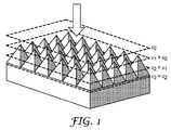
本発明の一態様は、少なくとも1つの微細構造化表面又は界面を有する、電磁波アイソレータである。微細構造化表面又は界面は、微細構造化部分(複数を含む)の深さにわたる電磁特性の変化を提供する。変化は、斬進的変化又は段階的変化であってもよい。本発明の電磁波アイソレータは、その物理的特徴により、少なくとも部分的に電磁特性におけるこの変化を達成する。これは、アイソレータの各層を作製するために使用される材料の電磁特性の変化による、又はアイソレータの特定の層内の組成勾配によって、アイソレータの深さにわたる電磁特性の変化を達成する、先行技術の電磁波アイソレータとは対照的である。図1は、錐体形の微細構造化表面を有する、本発明の電磁波アイソレータを例示し、微細構造化部分における、等価誘電率(ε0;ε1>ε0;ε2>ε1;及びε3>ε2)の一部の例示的な平面を示す。透過率といった他の電磁特性が、対応して同様の変形例を有するであろう。少なくとも1つの実施形態において、微細構造化部分は、微細構造化特徴の周期性、又は周期性及び高さの少なくとも1つが、アイソレータ材料内の電磁波長未満であるときに、電磁特性勾配を効果的に提供する。微細構造化周期性よりもはるかに大きな電磁波長に関して、微細構造化部分(複数を含む)は、電磁特性が、微細構造化部分の表面又は界面の形状に依存して、自由空間(若しくは異なる材料)から、基底部分、即ち、微細構造化部分と同じ材料でできているが、微細構造化特徴部を含有しない、微細構造化部分に隣接する微細構造化アイソレータセクションの部分へと変化する、媒体を作成する。電磁特性、微細構造化パターン、全体的なアイソレータ厚さ、及び微細構造化部分の厚さの基底部分の厚さに対する比率の適切な整合により、構成物の反射率及び/又はアイソレータ特徴部は、特定のアンテナ設計に対して強化することができる。アイソレータ媒体における波長が、微細構造化パターンの周期性未満である、電磁周波数に関して、本発明の少なくとも1つの実施形態において、微細構造化特徴部は、アイソレータ構成物におけるその領域内の有効な電磁特性を変化させる方法としての役割をする。アイソレータ媒体における波長は、λo(εrμr)−1/2によって求められる。εr=300、μr=1、及び2mmの周期性を有する微細構造化特徴部を有するアイソレータに関して、遮断周波数は、約9GHzである。微細構造化された錐体形のアレイを有するアイソレータは、約9GHzよりも低い電磁放射に対して、微細構造化領域内で連続的に変化する誘電率を有するかのように挙動するであろう。約9GHzを上回ると、微細構造化特徴部は、より別個の構造として挙動する。εr=30、μr=1、及び0.3mmの周期性を有する微細構造化特徴部を有するアイソレータに関して、遮断周波数は、約200GHzである。 One aspect of the present invention is an electromagnetic wave isolator having at least one microstructured surface or interface. The microstructured surface or interface provides a change in electromagnetic properties across the depth of the microstructured portion (s). The change may be a radical change or a step change. The electromagnetic isolator of the present invention achieves this change in electromagnetic characteristics, at least in part, due to its physical characteristics. This is due to the change in the electromagnetic properties of the material used to make each layer of the isolator, or to the change in the electromagnetic properties across the depth of the isolator, due to the compositional gradient within a particular layer of the isolator. In contrast to electromagnetic isolators. FIG. 1 illustrates an electromagnetic isolator of the present invention having a cone-shaped microstructured surface, wherein the equivalent permittivity (ε 0 ; ε 1 > ε 0 ; ε 2 > ε 1 ; and ε in the microstructured portion. 3 shows some exemplary planes of 3 > ε 2 ). Other electromagnetic properties, such as transmittance, will correspondingly have similar variations. In at least one embodiment, the microstructured portion effectively reduces the electromagnetic property gradient when the periodicity of the microstructured feature, or at least one of the periodicity and height is less than the electromagnetic wave length in the isolator material. To provide. For electromagnetic wave lengths that are much larger than the microstructured periodicity, the microstructured part (s) are free space (or different materials) depending on the shape of the surface or interface of the microstructured part. ) To a portion of the microstructured isolator section adjacent to the microstructured portion that is made of the same material as the base portion, ie, the microstructured portion, but does not contain the microstructured features Create With proper matching of electromagnetic properties, microstructured pattern, overall isolator thickness, and ratio of microstructured portion thickness to base portion thickness, the reflectivity of components and / or isolator features can be: It can be enhanced for specific antenna designs. With respect to electromagnetic frequencies, where the wavelength in the isolator medium is less than the periodicity of the microstructured pattern, in at least one embodiment of the invention, the microstructured features are effective electromagnetic properties within that region of the isolator construction. To act as a way to change The wavelength in the isolator medium is determined by λ o (ε r μ r ) −1/2 . For an isolator with a microstructured feature having a periodicity of ε r = 300, μ r = 1, and 2 mm, the cutoff frequency is about 9 GHz. Isolators with microstructured cone-shaped arrays will behave as if they have a dielectric constant that varies continuously within the microstructured region for electromagnetic radiation below about 9 GHz. Above about 9 GHz, the microstructured features behave as more discrete structures. For an isolator having a microstructured feature with ε r = 30, μ r = 1, and a periodicity of 0.3 mm, the cutoff frequency is about 200 GHz.
本発明の少なくとも1つの実施形態において、微細構造化表面は、アンテナの全体平面に平行ではない界面を作成(又は提供)し、界面の両側のアイソレータの界面及び隣接する3次元の特徴部は、対照的な電磁特性の材料を含む容積を画定する。 In at least one embodiment of the present invention, the microstructured surface creates (or provides) an interface that is not parallel to the overall plane of the antenna, and the interface of the isolator on both sides of the interface and the adjacent three-dimensional features are: A volume containing a material of contrasting electromagnetic properties is defined.
本発明の電磁波アイソレータの少なくとも1つの実施形態は、少なくとも1つの表面が、特徴部の反復するアレイを有するように、構成体に形成される、高誘電率及び/又は高透過率充填剤材料が填加された結合剤材料を含む。高誘電率及び/又は高透過率充填剤が填加された結合剤材料は、ウェブベースのプロセスにあるように、連続的な微細構造化フィルム又はシートに形成することができるか、又はそれは、非常に特異的な形状若しくは用途のために設計されるものといった、個々の部品を産生するプロセスにおいて利用することができる。典型的に、材料は、約80重量%〜約95重量%の充填剤を含む。しかしながら、量は、結合剤及び充填剤の特定の重力、並びに粒子の形状、結合剤との粒子の相溶性、製造プロセスのタイプ、溶媒を使用するかどうか、及びどのタイプの溶媒を使用するか等といった、他のパラメータに極めて依存する。 At least one embodiment of the electromagnetic isolator of the present invention is a high dielectric constant and / or high transmittance filler material formed in a construction such that at least one surface has a repeating array of features. Contains filled binder material. The binder material loaded with a high dielectric constant and / or high permeability filler can be formed into a continuous microstructured film or sheet, as in a web-based process, or It can be utilized in processes that produce individual parts, such as those designed for very specific shapes or applications. Typically, the material includes from about 80% to about 95% filler by weight. However, the amount depends on the specific gravity of the binder and filler, as well as the shape of the particles, the compatibility of the particles with the binder, the type of manufacturing process, whether a solvent is used and what type of solvent is used Etc., very dependent on other parameters.
本発明の少なくとも1つの実施形態において、結合剤(典型的に、少濃度)は、高誘電率又は高透過率材料と混合することができ、微細構造化パターンを形成することができ、結合剤は蒸発又は焼失させることができ、構成物を焼結することができる。 In at least one embodiment of the present invention, a binder (typically a low concentration) can be mixed with a high dielectric constant or high transmittance material to form a microstructured pattern, and the binder Can be evaporated or burned off and the composition can be sintered.
好適な結合剤としては、熱可塑材、熱硬化材、硬化性液体、熱可塑性エラストマー、又は充填剤を分散及び結合するための他の既知の材料が挙げられる。具体的な好適な材料としては、ポリエチレン、ポリプロピレン、シリコーン、シリコーンゴム、ポリオレフィンコポリマー、EPDM等といった、比較的非極性の材料;塩素化ポリエチレン、アクリレート、ポリウレタン等といった、極性材料;及びエポキシ、アクリレート、ウレタン等といった硬化性材料;及び非硬化性材料が挙げられる。本発明のアイソレータを作製するために使用される結合剤材料は、ガラス泡、空気(例えば、泡を作成するため)、及びTEFLON(登録商標)といったポリテトラフルオロエチレン(PTFE)を含む、異なるタイプの低誘電率充填剤が填加されてもよい。TEFLON(登録商標)といったPTFEもまた、結合剤として単独で使用されてもよい。本発明のアイソレータの1つ以上のセクションを作製するために使用される材料は、充填剤がより自由に流れ、使用される場合、結合剤に混合することを可能にし、粒子のより高濃度でのより効果的な混合を可能にするように、高誘電率又は高透過率充填剤と混合される、米国特許公開第2008/0153963号に説明されるものといった、少濃度の相溶剤処理したナノ粒子が填加されてもよい。 Suitable binders include thermoplastics, thermosets, curable liquids, thermoplastic elastomers, or other known materials for dispersing and bonding fillers. Specific suitable materials include relatively non-polar materials such as polyethylene, polypropylene, silicone, silicone rubber, polyolefin copolymers, EPDM, etc .; polar materials such as chlorinated polyethylene, acrylate, polyurethane, etc .; and epoxy, acrylate, Curable materials such as urethane; and non-curable materials. The binder materials used to make the isolator of the present invention are different types, including glass foam, air (eg, to create foam), and polytetrafluoroethylene (PTFE) such as TEFLON®. A low dielectric constant filler may be added. PTFE such as TEFLON (R) may also be used alone as a binder. The material used to make one or more sections of the isolator of the present invention allows the filler to flow more freely and, if used, mix with the binder and at higher concentrations of particles. Small concentrations of compatibilized nanofibers, such as those described in US 2008/0153963, mixed with high dielectric constant or high permeability fillers to allow more effective mixing of Particles may be added.
本発明のアイソレータの1つ以上のセクションを作製するために使用される材料は、フェライト材料(Trans−Tech IncからのCO2Z)、商標名でSENDUSTと称されるが、KOOL Mu(Magnetics Inc、www.mag−inc.com)といった他の商品名でも入手可能な鉄/シリコン/アルミニウム材料、商品名PERMALLOYで入手可能な鉄/ニッケル材料、又はCarpenter Technologies Corporation(www.cartech.com)から入手可能なその鉄/ニッケル/モリブデン類MOLYPERMALLOY、並びにアニールされていない、アニールされた、及び任意にリン酸若しくは何らかの他の表面不動態化剤で処理されてもよい、カルボニル鉄といった、軟質磁性材料が填加されてもよい。軟質磁性材料は、球体、プレート、フレーク、ロッド、繊維、無定形といった、種々の形状を有してもよく、マイクロ又はナノサイズであってもよい。 The material used to make one or more sections of the isolator of the present invention is a ferrite material (CO2Z from Trans-Tech Inc), referred to by the trade name SENDUST, but with KOUL Mu (Magnetics Inc, www. Iron / silicon / aluminum materials available under other trade names such as .mag-inc.com), iron / nickel materials available under the trade name PERMALLOY, or available from Carpenter Technologies Corporation (www.cartech.com) Its iron / nickel / molybdenum MOLYPERMALLOY and carbonyls that have not been annealed, annealed, and optionally treated with phosphoric acid or some other surface passivating agent A soft magnetic material such as iron may be filled. The soft magnetic material may have various shapes such as spheres, plates, flakes, rods, fibers, and amorphous, and may be micro or nano-sized.
代替的に、本発明のアイソレータの1つ以上のセクションを作製するために使用される材料は、チタン酸バリウム、チタン酸ストロンチウム、二酸化チタン、カーボンブラック、又は米国仮特許出願第61/286247号に説明される炭素修飾チタン酸バリウム材料を含む他の既知の高誘電率材料を含む、異なるタイプの高誘電率充填剤が填加されてもよい。ナノサイズの高誘電率粒子及び/又は高誘電率共役ポリマーもまた、使用されてもよい。2つ以上の異なる高誘電率材料の混合、又はカルボニル鉄といった高誘電率材料及び軟質磁性材料の混合が使用されてもよい。 Alternatively, the materials used to make one or more sections of the isolator of the present invention are barium titanate, strontium titanate, titanium dioxide, carbon black, or US Provisional Patent Application No. 61/286247. Different types of high dielectric constant fillers may be loaded, including other known high dielectric constant materials including the carbon-modified barium titanate material described. Nano-sized high dielectric constant particles and / or high dielectric constant conjugated polymers may also be used. A mixture of two or more different high dielectric constant materials or a mixture of a high dielectric constant material such as carbonyl iron and a soft magnetic material may be used.
本発明の少なくとも1つの実施形態において、結合剤及び高誘電率材料を使用する代わりに、1つの好適な材料の例は、約3000の誘電率を有するポリアニリン/エポキシ混合である(J.Lu et al.,「High dielectric constant polyaniline/epoxy composites via in situ polymerization for embedded capacitor applications」,Polymer,48(2007),1510〜1516)。 In at least one embodiment of the present invention, instead of using a binder and a high dielectric constant material, an example of one suitable material is a polyaniline / epoxy blend having a dielectric constant of about 3000 (J. Lu et al. al., “High dielectric constant polyaniline / epoxy composites via in situ polymerization for embedding capacitor applications”, Polymer, 48 (15).
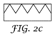
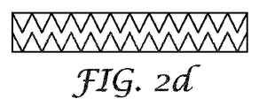
微細構造化パターンは、本発明のアイソレータの1つの外面上;同じパターンを有するアイソレータの両方の外面上;又は、異なるパターン及び/又は周期性を有するアイソレータの両方の外面上に存在してもよい。微細構造化パターンは、異なる材料を含むセクションの界面において、本発明のアイソレータ内に存在してもよい。微細構造化パターンは、アイソレータ内の1つ以上の界面に存在してもよい。2つ以上の界面が存在する場合、パターンは、異なる界面に対して、同じ又は異なっていてもよい。図2a〜2lは、これらの変形例の一部を示す本発明の異なる実施形態を例解する。図2aは、1つの微細構造化表面を有する物品を示す。図2bは、2つの対向する微細構造化表面を有する物品を示す。図2cは、1つの微細構造化界面を有する物品を示す。界面は、典型的に、表面上に微細構造化特徴部を有する第1のセクションを作成すること、次いで、微細構造化特徴によって作成される開放領域を、微細構造化表面を有するセクションを形成する材料とは異なる材料で充填することによって形成される。本発明の少なくとも1つの実施形態において、異なる材料は第1のセクションを形成する材料とは異なる誘電率及び/又は異なる透過率を有してもよい。異なる材料は、意図される用途に対してアイソレータをより細かく調整するために使用することができる。本発明の少なくとも1つの実施形態において、第1及び第2のセクション(及び任意に追加のセクション)を形成する材料は、異なる透過率を有し、2つのセクションに対する透過率値は約3〜約1000の比率を有する。本発明の少なくとも1つの実施形態において、第1及び第2のセクション(及び任意に追加のセクション)を形成する材料は異なる誘電率を有し、2つのセクションに対する誘電率値は、約2.5〜約1000の比率を有する。異なる材料は、所望の電磁特性を提供することができる、任意の好適な材料であってもよく、ポリマー、樹脂、接着剤等が挙げられるが、これらに限定されない。それらは、任意に、システムの電磁特性を調整するための充填剤を含んでもよい。開放領域を材料で充填することの代替として、開放領域は、空のままとすることができ、この場合、空気が、異なる材料として機能する。例えば、図2a及び図2bを参照のこと。異なる材料が、微細構造化表面周囲の開放領域を充填する(このため、界面を形成する)ときに、電磁特性は、微細構造化表面又は界面の形状、及びアイソレータの種々のセクションを形成する材料の特性に従って、物品の1つの外面から他方の外面まで変化する。アイソレータは、任意に、1つ若しくは両方の外面上に接着剤セクションを備えてもよいか、又は接着剤は、2つの非接着剤セクション間の内部セクションを形成し得る。接着剤は、微細構造化特徴によって作成される開放領域を充填する異なる材料として使用されてもよい。アイソレータの外面を形成する材料が、接着剤ではない場合、接着剤層をアイソレータ物品に塗布して、それを物体に固定してもよい。 The microstructured pattern may be present on one outer surface of the isolator of the present invention; on both outer surfaces of the isolator having the same pattern; or on both outer surfaces of the isolator having different patterns and / or periodicities. . The microstructured pattern may be present in the isolator of the present invention at the interface of sections comprising different materials. The microstructured pattern may be present at one or more interfaces within the isolator. If more than one interface is present, the pattern may be the same or different for different interfaces. Figures 2a to 21 illustrate different embodiments of the invention showing some of these variations. FIG. 2a shows an article having one microstructured surface. FIG. 2b shows an article having two opposing microstructured surfaces. FIG. 2c shows an article with one microstructured interface. The interface typically creates a first section having a microstructured feature on the surface, and then forms an open area created by the microstructured feature into a section having a microstructured surface. It is formed by filling with a material different from the material. In at least one embodiment of the present invention, the different material may have a different dielectric constant and / or a different transmittance than the material forming the first section. Different materials can be used to fine tune the isolator for the intended application. In at least one embodiment of the present invention, the materials forming the first and second sections (and optionally additional sections) have different transmissions, and the transmission values for the two sections are about 3 to about It has a ratio of 1000. In at least one embodiment of the present invention, the materials forming the first and second sections (and optionally additional sections) have different dielectric constants, and the dielectric constant values for the two sections are about 2.5. Has a ratio of ~ 1000. The different material may be any suitable material that can provide the desired electromagnetic properties, including but not limited to polymers, resins, adhesives, and the like. They may optionally include a filler to adjust the electromagnetic properties of the system. As an alternative to filling the open area with material, the open area can be left empty, in which case air functions as a different material. For example, see FIGS. 2a and 2b. When different materials fill the open area around the microstructured surface (and thus form an interface), the electromagnetic properties are the material that forms the microstructured surface or interface shape, and the various sections of the isolator Varies from one outer surface of the article to the other outer surface. The isolator may optionally comprise an adhesive section on one or both outer surfaces, or the adhesive may form an internal section between two non-adhesive sections. The adhesive may be used as a different material that fills the open areas created by the microstructured features. If the material forming the outer surface of the isolator is not an adhesive, an adhesive layer may be applied to the isolator article to secure it to the object.
アイソレータ物品はまた、アイソレータ、及び、例えば、付随するタグ若しくはアンテナがそれに対して配置される物体にかかわらず、アンテナ若しくはタグが、同じ読取範囲を有するように、金属又は導電性層を含んでもよい。かかる場合、アンテナ又はタグ/アイソレータ部分は、存在する金属層と良好に動作するように調整され、次いで、システムは、金属物品又は段ボールといった低誘電率材料に対して配置されるかどうかにかかわらず、等しく良好に動作する。 An isolator article may also include a metal or a conductive layer so that the antenna or tag has the same read range, regardless of the isolator and, for example, the object to which the associated tag or antenna is placed. . In such a case, the antenna or tag / isolator portion is tuned to work well with the metal layer present, and then the system is either placed against a low dielectric constant material such as a metal article or cardboard. Works equally well.
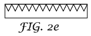
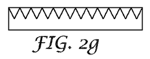
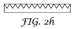
先で述べられるように、1つ以上の微細構造化表面又は界面を有する物品は、2つ以上のセクションを有してもよく、そのセクションは、異なる誘電率及び/又は透過率を有する材料を含む。図2dは、3つのセクションの各々が、異なる材料を含み、異なる特性を有する本発明の3つのセクション/2つの界面の物品の例を例示する。本発明の物品の実施形態は、無数の異なる構成を有してもよい。例えば、図2e及び2fは、同じ全体の厚さを有するが、物品の2つのセクションを成す材料の異なる比率を有する、発明の物品を例示する。図2g及び2hは、2つの材料の比率は同じであるが、物品の全体的な厚さが異なる、本発明の物品を例示する。 As mentioned above, an article having one or more microstructured surfaces or interfaces may have two or more sections, which sections are made of materials having different dielectric constants and / or transmittances. Including. FIG. 2d illustrates an example of a three section / two interface article of the invention where each of the three sections comprises a different material and has different properties. Embodiments of the article of the present invention may have a myriad of different configurations. For example, FIGS. 2e and 2f illustrate inventive articles that have the same overall thickness, but have different proportions of material that make up two sections of the article. Figures 2g and 2h illustrate an article of the invention in which the ratio of the two materials is the same, but the overall thickness of the article is different.
微細構造化特徴部及び微細構造化特徴部のパターンはまた、本発明の特定の実施形態に基づいて、変化してもよい。例えば、セクションの同じ全体的な厚さ及び同じ相対比率を有する物品において、勾配の長さは、図2i及び2jに例示されるように異なってもよい。他の実施形態において、微細構造化特徴部の横方向の間隔もまた、変化してもよい。例えば、図2k及び2lによって例示されるように、微細構造化特徴部の幅及び数は、変化してもよい。 The microstructured features and the pattern of the microstructured features may also vary based on certain embodiments of the invention. For example, in articles having the same overall thickness and the same relative proportion of sections, the length of the gradient may be different as illustrated in FIGS. 2i and 2j. In other embodiments, the lateral spacing of the microstructured features may also vary. For example, as illustrated by FIGS. 2k and 21, the width and number of microstructured features may vary.
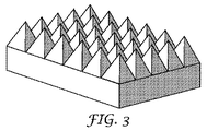
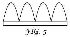
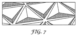
連続的に変化する電磁特性勾配を提供する微細構造化特徴部は、かかる特徴部を有するセクションの基底部分の主軸に非水平及び非垂直の表面を有する特徴部を含む。例示的な特徴部としては、鋭い、90°、若しくは傾斜した頂角を有する、正方形を基底とした錐体(図3)、鋭い、傾斜した、若しくは立方体コーナ頂角を有する三角形を基底とした錐体(図7)、鋭い若しくは傾斜した頂角を有する六角形を基底とした錐体、回転した錐体、及び円形若しくは楕円形基底を有する円錐、鋭い、90°、若しくは傾斜した頂角を有する円錐といった、オフセット頂点(例えば、鋸歯状錐体)円錐を有してもよい、非対称錐体といった、錐体、放物体(図5)、三角形のプリズム(図6)、並びに半球体が挙げられるが、これらに限定されない。採用される微細構造のタイプに依存して、電磁特性勾配は、構成物の片側から他方の側に直線的に変化し得る。勾配はまた、放物線状であり得、他の機能性を備え得る。 Microstructured features that provide a continuously varying electromagnetic characteristic gradient include features having non-horizontal and non-vertical surfaces on the principal axis of the base portion of the section having such features. Exemplary features include a square-based pyramid (FIG. 3) with a sharp, 90 °, or tilted apex angle, a triangle with a sharp, tilted, or cube-corner apex angle as the basis. A cone (FIG. 7), a cone based on a hexagon with a sharp or inclined apex angle, a rotated cone, and a cone with a round or elliptical base, a sharp, 90 ° or inclined apex angle Examples include cones, paraboloids (FIG. 5), triangular prisms (FIG. 6), and hemispheres such as asymmetric cones that may have offset vertices (eg, serrated cones) cones. However, it is not limited to these. Depending on the type of microstructure employed, the electromagnetic property gradient can vary linearly from one side of the component to the other. The gradient may also be parabolic and may have other functionality.
電磁特性において段階的な勾配を提供する微細構造化特徴部は、かかる特徴部を有するアイソレータのセクションの基底部分の主軸に水平及び垂直の表面を有するものを含む。例示的な特徴としては、円形、正方形、及び三角形の水平の断面を有するものを含む支柱(図8);平行6面体;並びにセクションの基底部分に単に平行及び垂直の(即ち、傾斜していない)表面を有する、他の同様のブロック構造が挙げられるが、これらに限定されない。種々の実施形態において、微細構造化特徴部の横方向の間隔、及び個々の微細構造化特徴部の基底間の間隔は、変化してもよい。 Microstructured features that provide a graded gradient in electromagnetic properties include those having horizontal and vertical surfaces on the principal axis of the base portion of the section of the isolator having such features. Exemplary features include columns having circular, square, and triangular horizontal cross-sections (FIG. 8); parallelepipeds; and simply parallel and perpendicular (ie, not inclined) to the base portion of the section ) Other similar block structures having a surface include, but are not limited to: In various embodiments, the lateral spacing of the microstructured features and the spacing between the bases of the individual microstructured features may vary.
一部の微細構造化特徴部は、電磁特性における勾配を効果的に提供する、複数の小さな段階的変化を有する。かかる構造の例は、図4における非対称の段階的な錐体である。他の例は、複数の小さな増分で変化する形状を含む。 Some microstructured features have multiple small step changes that effectively provide a gradient in electromagnetic properties. An example of such a structure is the asymmetric step cone in FIG. Other examples include shapes that change in multiple small increments.
一部の微細構造特徴部又はパターンは、連続的及び段階的な勾配の組み合わせを提供する、形状又は配設を有する。例えば、角錐台及び円錐台は、その上部(水平の)表面においては、段階的な勾配を提供するが、その側部(傾斜した)表面においては、連続的な勾配を提供するであろう。別の例として、図6のブレードアレイにおいて、三角形のプリズムの傾斜した表面は、連続的な勾配を提供するが、三角形のプリズムの垂直の表面は、アイソレータの基底に垂直の表面を提供するであろう。 Some microstructure features or patterns have shapes or arrangements that provide a combination of continuous and stepped gradients. For example, the pyramid and frustum will provide a graded gradient on its upper (horizontal) surface, but a continuous gradient on its side (tilted) surface. As another example, in the blade array of FIG. 6, the inclined surface of the triangular prism provides a continuous gradient, while the vertical surface of the triangular prism provides a surface perpendicular to the base of the isolator. I will.
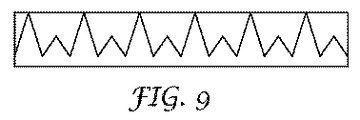
一部の実施形態において、本発明の微細構造化特徴部のパターンは、高さ(図9)、幅、形状、横方向の間隔、周期性等に関して、二峰性又は三峰性といった多峰性であってもよい。 In some embodiments, the microstructured feature pattern of the present invention is multimodal, such as bimodal or trimodal, with respect to height (FIG. 9), width, shape, lateral spacing, periodicity, etc. It may be.
得られる製品は、時折、それらを作製するために使用されるプロセスに依存して、いくつかの異なる形態を採ってもよい。例えば、連続的なシート又はウェブベースのプロセスは、ロール形態の製品を産生するために使用されてもよく、これは、後に、特定の用途のために切断又はサイズ決定することができる。得られる製品は、特定の製品設計を満たしつつ、無駄を最小化するように、長方形、楕円形、又は更には複雑な2D形状といった異なる形状に直接成形されてもよい。 The resulting products sometimes take several different forms depending on the process used to make them. For example, a continuous sheet or web-based process may be used to produce a product in roll form, which can later be cut or sized for a particular application. The resulting product may be directly molded into different shapes, such as rectangular, elliptical, or even complex 2D shapes to meet specific product designs while minimizing waste.
種々の微細構造化方法が、本発明の微細構造化表面又は界面を形成するのに好適である。好適な方法としては、カレンダ加工;高圧力エンボス加工;鋳型を用いた鋳造及び硬化(例えば、結合剤を有する高誘電率又は透過率材料して(この結合剤は、材料が鋳型上で鋳造された後、硬化される));圧縮成形(例えば、鋳型、及び結合剤を有する高誘電率又は透過率材料が、加熱され、次いで、鋳型が、材料に対して押圧される);押出鋳造(例えば、結合剤を有する高誘電率又は透過率材料が、加熱されたツールに直接押出され、ツールが冷却され、形成された材料が、ツールから取り出される);押出エンボス加工(例えば、結合剤を有する高誘電率又は透過率材料が、低温のツールに直接押出され、次いで、ツールから取り出される);火炎エンボス加工(例えば、結合剤を有する高誘電率又は透過率材料の表面のみを加熱するために火炎を使用し、次いで、表面をツールを用いて微細構造化する);並びに射出成形(例えば、結合剤を有する融解された高誘電率又は透過率材料を、加熱された鋳型に射出し、次いで、冷却する)が挙げられる。次いで、これらのシステムの各々は、微細構造化部分上で、成形又は硬化される、対照的な電磁特性を有する材料を有し得る。代替的に、最初の微細構造化は、低透過率及び誘電率を有する材料とともに実施され得、次いで、対照的な電磁特性を有する材料が、その上で成形又は硬化され得る。 A variety of microstructured methods are suitable for forming the microstructured surface or interface of the present invention. Suitable methods include: calendering; high pressure embossing; casting and curing with a mold (eg, a high dielectric constant or permeability material with a binder (this binder is cast on the mold) And then cured)); compression molding (e.g., a mold and a high dielectric constant or permeable material with a binder is heated and then the mold is pressed against the material); extrusion casting ( For example, a high dielectric constant or transmissive material with a binder is extruded directly into a heated tool, the tool is cooled, and the formed material is removed from the tool); High dielectric constant or transmissive material having been extruded directly into a cold tool and then removed from the tool); flame embossing (eg, heating only the surface of the high dielectric constant or transmissive material with the binder) Using a flame to make the surface then microstructured with a tool); as well as injection molding (eg, injecting a molten high dielectric constant or transmission material with a binder into a heated mold) And then cooling). Each of these systems can then have a material with contrasting electromagnetic properties that is molded or cured on the microstructured portion. Alternatively, the initial microstructure can be performed with a material having a low transmission and dielectric constant, and then a material with contrasting electromagnetic properties can be molded or cured thereon.
本発明の実施形態は、超高周波数又は極超高周波数領域で動作するアンテナとともに使用するのに好適である。本発明の実施形態のアイソレータは、これらに限定されないが、携帯電話、通信アンテナ、ワイヤレスルータ、及びRFIDタグといった、用途において使用されてもよい。 Embodiments of the present invention are suitable for use with antennas operating in the very high frequency or very high frequency range. The isolators of embodiments of the present invention may be used in applications such as, but not limited to, mobile phones, communication antennas, wireless routers, and RFID tags.
本発明の実施形態は、RFIDチップを金属又は他の導電性表面から隔離するときといった、遠距離場電磁放射を含む用途において、特定の使用を見出す。本発明のアイソレータは、微細構造化パターンの周期性よりもはるかに長い、又は微細構造化パターンの高さよりもはるかに長い電磁波長を使用する用途に対して、適切である。 Embodiments of the present invention find particular use in applications involving far-field electromagnetic radiation, such as when isolating an RFID chip from metal or other conductive surfaces. The isolator of the present invention is suitable for applications that use electromagnetic lengths that are much longer than the periodicity of the microstructured pattern or much longer than the height of the microstructured pattern.
本発明の態様は、RFIDタグを導電性表面又は本体から隔離するために、本発明のアイソレータを使用するシステムを含む。受動UHF RFIDタグアンテナは、自由空間における、又は段ボール、木製パレット等といった、低誘電性材料上での使用に最適化される。UHF RFIDタグが、導電性表面又は本体に近接しているときに、タグアンテナのインピーダンス及び利得は変化し、読取器に給電する、及び応答するその能力を大幅に減少させる。 Aspects of the invention include systems that use the isolator of the invention to isolate RFID tags from conductive surfaces or bodies. Passive UHF RFID tag antennas are optimized for use in free space or on low dielectric materials such as cardboard, wooden pallets, etc. When a UHF RFID tag is in close proximity to a conductive surface or body, the impedance and gain of the tag antenna changes, greatly reducing its ability to power and respond to the reader.
導電性基材とRFIDタグとの間に配置されるアイソレータは、タグと基材(高透過率及び/又は誘電率)との間の距離を効果的に増加させることによって、並びに、導電性基材との相互作用からアンテナの磁場の能力を低減することによって(逆も同様)、金属基材の効果を向上させることができる。アイソレータの存在は、アンテナ利得だけでなく、アンテナの有効なインピーダンスもまた変化させることができ、このため、アンテナからRFID ICに移動される電力の量を変化させ、最終的に、電力は、RFID読取器に対して変調及び後方散乱される。これらの及び他の複雑な相互作用により、アイソレータ設計は、特定のRFIDタグに対して特異的である。同様の議論が、回路、又は金属筐体若しくは接地平面に近接した携帯電話アンテナといった、導電性材料に近い、他のタイプのアンテナに対しても当てはまる。 An isolator disposed between a conductive substrate and an RFID tag can effectively increase the distance between the tag and the substrate (high transmittance and / or dielectric constant), as well as the conductive group. By reducing the antenna's magnetic field capability from the interaction with the material (and vice versa), the effect of the metal substrate can be improved. The presence of the isolator can change not only the antenna gain, but also the effective impedance of the antenna, thus changing the amount of power transferred from the antenna to the RFID IC, and ultimately the power is Modulated and backscattered to reader. Due to these and other complex interactions, the isolator design is specific to a particular RFID tag. Similar arguments apply to other types of antennas that are close to conductive materials, such as circuits or cellular antennas close to a metal enclosure or ground plane.
RFIDタグは、多様な顧客の必要性を満たすように、無数の異なる設計で供給される。RFID IC設計における相違の一部は、電力、メモリ、及び計算能力におけるそれらの相違と関係する。RFIDアンテナ設計は、ICとインピーダンスを整合させる必要性、所望の読取距離、設置面積の最小化、設置面積のアスペクト比、及び向きの応答依存性を含むいくつかの要因によって決定付けられる。多数の設計のRFIDタグは、Intermec Technologies Corporation、Alien Technology、Avery−Dennison、及びUPM Raflatacといった、いくつかの企業のいずれからも購入することができる。 RFID tags are supplied in myriad different designs to meet the needs of diverse customers. Some of the differences in RFID IC design are related to those differences in power, memory, and computing power. RFID antenna design is dictated by several factors including the need to match impedance with the IC, desired read distance, footprint minimization, footprint area aspect ratio, and orientation response dependence. Numerous designs of RFID tags can be purchased from any of several companies, such as Intermec Technologies Corporation, Allien Technologies, Avery-Denison, and UPM Raflatac.
UHF RFIDタグは、典型的に、865〜954MHzの周波数範囲において動作し、最も典型的な中心周波数は、869MHz、915MHz、及び953MHzである。RFIDタグは、バッテリといった電源を含むことによって、自己給電することができる。代替的に、それは、それが、基地局によって伝送されている電磁波のエネルギーを捕捉すること、及びそのエネルギーをDC電圧に変換することによって、その内部電力を生成するように、フィールド給電することができる。 UHF RFID tags typically operate in the frequency range of 865 to 954 MHz, with the most typical center frequencies being 869 MHz, 915 MHz, and 953 MHz. An RFID tag can be self-powered by including a power source such as a battery. Alternatively, it can be field fed so that it generates its internal power by capturing the energy of the electromagnetic wave being transmitted by the base station and converting that energy into a DC voltage. it can.
本発明のアイソレータは、タグ付けされる物品の電気特性が、RFIDタグの動作を妨害するときに、最も有用である。これは、タグ付けされる物品が、金属基材を備えるか、又は、液体を収容するように構成されるときに(これらは両方とも、読取距離に関して問題である)、最もしばしば生じる。 The isolator of the present invention is most useful when the electrical properties of the item being tagged interfere with the operation of the RFID tag. This most often occurs when the article to be tagged comprises a metal substrate or is configured to contain a liquid (both of which are problematic with respect to read distance).
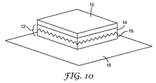
図10は、RFIDタグ10と、セクション14及び16を備えるアイソレータ12と、タグ付けされる物品18を含む、本発明のシステムを例示する。接着剤層(図示せず)は、関連するアイソレータセクション14、16が、RFIDタグ又はタグ付けされる物品18に接着するための十分な接着剤特性を有しない場合、RFIDタグ10とセクション14及び/又はセクション16、及びタグ付けされる物品18との間に、追加的に追加されてもよい。
FIG. 10 illustrates the system of the present invention including an
本発明は、以下の実施例によって更に例示されるが、これらの実施例において列挙された特定の材料及びその量は、他の諸条件及び詳細と同様に、本発明を不当に制限するものと解釈すべきではない。 The invention is further illustrated by the following examples, but the specific materials and amounts listed in these examples, as well as other conditions and details, should unduly limit the invention. Should not be interpreted.
試験及び測定方法
等価厚の計算
「等価厚」は、微細構造化構造が、微細構造化特徴部を有しない、中実セクションを作成するように平坦化される場合に、セクションがなるであろう厚さを意味する。
Test and Measurement Methods Equivalent Thickness Calculation "Equivalent Thickness" will be a section when the microstructured structure is flattened to create a solid section with no microstructured features It means thickness.
注意:RFIDシステムが作製された全ての実施例において、両面テープ(SCOTCH 665、3M Company)の1つの層は、アイソレータが金属基材に接着したままであることを確実とするように、金属基材(アルミニウムプレート又は3M Companyより入手可能な3M(商標)EMI Tin−Plated Copper Foil Shielding Tape 1183(以降、「1183 Tape」と称される場合がある)のいずれか)と、アイソレータとの間で接着された。 Note: In all embodiments in which the RFID system is made, one layer of double-sided tape (SCOTCH 665, 3M Company) is used to ensure that the isolator remains adhered to the metal substrate. Between the material (either aluminum plate or 3M ™ EMI Tin-Plate Copper Foil Shielding Tape 1183 available from 3M Company) (hereinafter sometimes referred to as “1183 Tape”) and the isolator Glued.
実施例1〜3及び比較実施例(CE)A〜F
比較実施例A〜Fの調製
58重量%のTiO2/42重量%のシリコーンの割合で、TiO2(TIPURE R−902+、Dupont Inc.、www2.dupont.com)を、シリコーン(SYLGARD 184、Dow Corning、www.dowcorning.com)に混合し、種々の厚さで一体式の2.5cm×10cmのスラブに硬化した。85重量%のカルボニル鉄/15重量%のシリコーンの割合で、カルボニル鉄粉末(ER Grade、BASF、www.inorganics.basf.com)を、シリコーン(SYLGARD 184、Dow Corning、www.dowcorning.com)に混合し、種々の厚さで一体式の2.5cm×10cmのスラブに硬化した。比較実施例A〜Cは、0.51mm厚の58%のTiO2/シリコーン混合セクション、並びにそれぞれ0.72、1.02、及び1.29mmの厚さのカルボニル鉄/シリコーン混合セクションを有した。比較実施例D〜Fは、0.72mm厚の58%のTiO2/シリコーン混合セクション、並びにそれぞれ0.48、0.72、及び1.02mmの厚さのカルボニル鉄/シリコーン混合セクションを有した。
Examples 1-3 and Comparative Examples (CE) A-F
At a rate of Comparative Example A~F Preparation 58 wt% of TiO 2/42 wt% silicone, TiO 2 (TIPURE R-902 +, Dupont Inc., www2.dupont.com) a silicone (SYLGARD 184, Dow Coming, www.dowcorning.com) and cured into monolithic 2.5 cm × 10 cm slabs of various thicknesses. Carbonyl iron powder (ER Grade, BASF, www.inorganics.basf.com) at a ratio of 85% by weight carbonyl iron / 15% by weight silicone to silicone (SYLGARD 184, Dow Corning, www.dowcorning.com). Mixed and cured into monolithic 2.5 cm × 10 cm slabs of various thicknesses. Comparative Examples AC had a 0.51 mm thick 58% TiO 2 / silicone mixed section and 0.72, 1.02, and 1.29 mm thick carbonyl iron / silicone mixed sections, respectively. . Comparative Examples D-F had a 0.72 mm thick 58% TiO 2 / silicone mixed section and carbonyl iron / silicone mixed sections 0.48, 0.72 and 1.02 mm thick, respectively. .
実施例1の調製
0.65mmの六方最密間隔で配設される、0.75mmの深さの円錐形の特徴部を備える、ニッケル鋳型を製作した。六方最密アレイは、2.5cm×10cmの領域を被覆した。58重量%のTiO2(TIPURE R−902+、Dupont Inc.、www2.dupont.com)をシリコーンシステム(SYLGARD 184、Dow Corning、www.dowcorning.com)に混合し、鋳型において硬化し、次いで取り出した。円錐の下のTiO2/シリコーン基底部分の厚さは、0.28mm厚であった。0.75mmの高さの円錐では、全体的なTiO2セクションの等価厚は、0.53mmであった。次いで、85重量%のカルボニル鉄粉末(ER Grade、BASF、www.inorganics.basf.com)を、シリコーン(SYLGARD 184、Dow Corning、www.dowcorning.com)に混合し、その混合を塗布して、TiO2充填円錐の周囲及び真上の空間を充填した。平滑な表面を作成するために、混合を、約0.29mm越えて、0.75mmの高さの円錐の上部に付加した。その後、混合を硬化した。
Preparation of Example 1 A nickel mold with a 0.75 mm deep conical feature disposed at 0.65 mm hexagonal close spacing was fabricated. The hexagonal close-packed array covered an area of 2.5 cm × 10 cm. 58 wt% of TiO 2 (TIPURE R-902 + , Dupont Inc., www2.dupont.com) were mixed silicone system (SYLGARD 184, Dow Corning, www.dowcorning.com ) , the cured in a mold and then removed . The thickness of the TiO 2 / silicone base under the cone was 0.28 mm thick. For a 0.75 mm high cone, the equivalent thickness of the overall TiO 2 section was 0.53 mm. Then 85% by weight of carbonyl iron powder (ER Grade, BASF, www.inorganics.basf.com) is mixed with silicone (SYLGARD 184, Dow Corning, www.dowcorning.com) and the mixture is applied, The space around and just above the TiO 2 filled cone was filled. In order to create a smooth surface, mixing was applied to the top of the cone of 0.75 mm height, exceeding about 0.29 mm. The mix was then cured.
実施例2〜3の調製
85重量%のER Gradeカルボニル鉄/15%のシリコーンを有する比較実施例A〜Fと同じように調製されたモノリシックのスラブは、実施例2及び3に関して、カルボニル鉄セクションの厚さを増加させるように、実施例1のカルボニル鉄側に対して配置された。実施例2及び3に関する一体式のスラブの厚さは、それぞれ、0.27mm及び0.48mmであった。シリコーンの接着特性により、完成物品をともに保持するのに接着剤は必要ない。
Preparation of Examples 2-3 Monolithic slabs prepared in the same manner as Comparative Examples AF having 85% by weight ER Grade carbonyl iron / 15% silicone were prepared with respect to Examples 2 and 3 in the carbonyl iron section. Was placed against the carbonyl iron side of Example 1 so as to increase the thickness. The thickness of the integral slab for Examples 2 and 3 was 0.27 mm and 0.48 mm, respectively. Due to the adhesive properties of silicone, no adhesive is required to hold the finished article together.
比較実施例A〜F及び実施例1〜3を使用するRFIDシステム
比較実施例A〜F及び実施例1〜3を使用するRFIDタグシステムは、Gen 2プロトコルで動作する、Avery Dennison 210 Runway RFIDタグを使用して作製した。タグは、12.5mm厚のアルミニウムプレートに近接して、902〜928MHzで読み取られた。RFIDタグシステムは、以下の順序の隣接するセクションで構築された:アルミニウムプレート/アイソレータのTiO2充填セクション/アイソレータのカルボニル鉄充填セクション/RFIDタグ。このシステムは、75%のRFIDタグ読取率が得られるまで、ALR−9780 Alien Readerの前の種々の位置で移動された。各比較実施例及び実施例に関して、75%の読取率における、ALR−9780読取器からの距離は、3つの独立した読取値で判定され、次いで、平均化された。
RFID System Using Comparative Examples A-F and Examples 1-3 The RFID tag system using Comparative Examples A-F and Examples 1-3 is an Avery Dennison 210 Runway RFID tag that operates with the
比較実施例に関する読取範囲データを表1に示す。2列目及び3列目は、それぞれ、TiO2/シリコーン混合セクション、及びカルボニル鉄/シリコーン混合セクションの実際の厚さを示す。表1は、読取範囲が、0.51mmのTiO2セクションの厚さに対して、カルボニル鉄セクションの厚さが、0.72〜1.29mmに増加したにつれて、単調に増加したことを示す。同様に、読取範囲は、TiO2セクションが0.73mm厚であったときに、カルボニル鉄セクションの厚さが、0.48〜1.02mmに増加したにつれて、単調に増加した。 Table 1 shows the reading range data relating to the comparative example. The second and third rows show the actual thickness of the TiO 2 / silicone mixed section and the carbonyl iron / silicone mixed section, respectively. Table 1 shows that the reading range monotonically increased as the thickness of the carbonyl iron section increased from 0.72 to 1.29 mm for a 0.51 mm TiO 2 section thickness. Similarly, the reading range monotonically increased as the thickness of the carbonyl iron section increased from 0.48 to 1.02 mm when the TiO 2 section was 0.73 mm thick.
実施例に関する読取範囲データを、表2に示す。2列目及び3列目は、それぞれ、TiO2及びカルボニル混合セクションの等価厚を示す。読取範囲は、0.53mmの有効なTiO2セクションの厚さとともに、等価のカルボニル鉄セクションの厚さが0.79〜1.27mmに増加したにつれて、単調に増加した。 Table 2 shows the reading range data regarding the example. The second and third rows show the equivalent thickness of the TiO2 and carbonyl mixed sections, respectively. The reading range increased monotonically with an effective TiO 2 section thickness of 0.53 mm as the equivalent carbonyl iron section thickness increased from 0.79 to 1.27 mm.
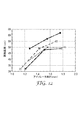
比較実施例A〜F及び実施例1〜3に関する読取範囲対アイソレータの厚さを、図11にともにプロットする。実線上のデータ点は、左から右に、実施例1、2、及び3を表す。大きなダッシュを伴う線上のデータ点は、左から右に、比較実施例A、B、及びCを表す。小さなダッシュを伴う線上のデータ点は、左から右に、比較実施例D、E、及びFを表す。比較実施例A〜Cは、本質的に実施例1〜3と同等のTiO2セクションの厚さを含む。いずれの所与のアイソレータの厚さにおいても、実施例1〜3は、比較実施例A〜Cよりも長い読取範囲を提供するということは明らかである。比較実施例におけるTiO2セクションの厚さの増加は、図11に例示されるように、読取距離における実質的な増加を示さなかった。 The read range versus isolator thickness for Comparative Examples A-F and Examples 1-3 are both plotted in FIG. Data points on the solid line represent Examples 1, 2, and 3 from left to right. Data points on the line with large dashes represent Comparative Examples A, B, and C from left to right. Data points on the line with small dashes represent Comparative Examples D, E, and F from left to right. Comparative Examples AC include essentially the same TiO 2 section thickness as Examples 1-3. It is clear that at any given isolator thickness, Examples 1-3 provide a longer reading range than Comparative Examples A-C. The increase in thickness of the TiO 2 section in the comparative example did not show a substantial increase in read distance, as illustrated in FIG.

実施例4〜6及び比較実施例(CE)G〜O
比較実施例G〜Oの調製
15重量%のXLD3000/85重量%のシリコーンの割合で、XLD3000ガラス泡(3M Company、www.3m.com)を、シリコーン(SYLGARD 184、Dow Corning、www.dowcorning.com)に混合し、種々の厚さで一体式の2.5cm×10cmのスラブに硬化した。85重量%のカルボニル鉄/15重量%のシリコーンの割合で、カルボニル鉄粉末(ER Grade、BASF、www.inorganics.basf.com)を、シリコーン(SYLGARD 184、Dow Corning、www.dowcorning.com)に混合し、種々の厚さで一体式の2.5cm×10cmのスラブに硬化した。比較実施例G〜Iは、0.41mmの15重量%のXLD3000/シリコーン混合セクションの厚さ、並びにそれぞれ0.72、1.02、及び1.29mmのカルボニル鉄/シリコーン混合セクションの厚さを有した。比較実施例J〜Lは、0.49mmの15重量%のXLD3000/シリコーン混合セクションの厚さ、並びにそれぞれ0.72、1.02、及び1.29mmのカルボニル鉄/シリコーン混合セクションの厚さを有した。比較実施例M〜Oは、0.54mmの15重量%のXLD3000/シリコーン混合セクションの厚さ、並びにそれぞれ0.72、1.02、及び1.29mmのカルボニル鉄/シリコーン混合セクションの厚さを有した。
Examples 4-6 and Comparative Example (CE) G-O
Preparation of Comparative Examples G-O XLD3000 glass foam (3M Company, www.3m.com) and silicone (SYLGARD 184, Dow Corning, www.dowcorning.) At a ratio of 15% by weight of XLD3000 / 85% by weight of silicone. com) and cured to a monolithic 2.5 cm × 10 cm slab with various thicknesses. Carbonyl iron powder (ER Grade, BASF, www.inorganics.basf.com) at a ratio of 85% by weight carbonyl iron / 15% by weight silicone to silicone (SYLGARD 184, Dow Corning, www.dowcorning.com). Mixed and cured into monolithic 2.5 cm × 10 cm slabs of various thicknesses. Comparative Examples GI have a thickness of 0.41 mm of 15 wt% XLD3000 / silicone mixed section, and 0.72, 1.02, and 1.29 mm carbonyl iron / silicone mixed sections respectively. Had. Comparative Examples J-L have a thickness of 0.49 mm of 15 wt% XLD3000 / silicone blend section and 0.72, 1.02, and 1.29 mm carbonyl iron / silicone blend sections respectively. Had. Comparative Examples M-O have a thickness of 0.54 mm 15 wt% XLD3000 / silicone blend section, and 0.72, 1.02, and 1.29 mm carbonyl iron / silicone blend sections respectively. Had.
実施例4の調製
0.59mmの正方形の間隔で配設される、0.36mmの深さの錐体特徴部を備えるニッケル鋳型を製作した。85重量%のカルボニル鉄粉末(ER Grade、BASF、www.inorganics.basf.com)を、シリコーンシステム(SYLGARD 184、Dow Corning、www.dowcorning.com)に混合し、鋳型において硬化し、次いで取り出した。錐体の下のカルボニル鉄/シリコーン基底部分の厚さは、0.70mm厚であった。0.36mmの高さの錐体では、全体的なカルボニル鉄セクションの等価厚は、0.82mmであった。シリコーンシステム(SYLGARD 184、Dow Corning、www.dowcorning.com)に混合した15重量%のXLD3000ガラス泡(3M Company、www.3m.com)を、塗布して、カルボニル鉄充填錐体の周囲及びその0.22mm上を充填し、次いで、硬化した。実施例4の合計の実際の厚さは、1.28mmであった。
Preparation of Example 4 A nickel mold with a 0.36 mm deep cone feature arranged at 0.59 mm square spacing was fabricated. 85% by weight of carbonyl iron powder (ER Grade, BASF, www.inorganics.basf.com) was mixed into a silicone system (SYLGARD 184, Dow Corning, www.dowcorning.com), cured in the mold, and then removed. . The thickness of the carbonyl iron / silicone base under the cone was 0.70 mm thick. For a 0.36 mm high cone, the equivalent carbonyl iron section equivalent thickness was 0.82 mm. 15% by weight XLD3000 glass foam (3M Company, www.3m.com) mixed with a silicone system (SYLGARD 184, Dow Corning, www.dowcorning.com) was applied around the carbonyl iron filled cone and its 0.22 mm top was filled and then cured. The total actual thickness of Example 4 was 1.28 mm.
実施例5〜6の調製
85重量%のER Gradeカルボニル鉄/15%のシリコーンの一体式のスラブを、実施例5及び6を作成するように、カルボニル鉄セクションの厚さを増加させるように、実施例4のカルボニル鉄側に対して配置された。実施例2及び3に関する一体式のスラブの厚さは、それぞれ、0.27mm及び0.48mmであった。シリコーンの接着特性により、完成物品をともに保持するのに接着剤は必要ない。
Preparation of Examples 5-6 An 85% by weight ER Grade carbonyl iron / 15% silicone monolithic slab to increase the thickness of the carbonyl iron section to create Examples 5 and 6, Arranged against the carbonyl iron side of Example 4. The thickness of the integral slab for Examples 2 and 3 was 0.27 mm and 0.48 mm, respectively. Due to the adhesive properties of silicone, no adhesive is required to hold the finished article together.
比較実施例G〜O及び実施例4〜6を使用するRFIDシステム
比較実施例G〜O及び実施例4〜6を使用するRFIDタグシステムは、Gen 2プロトコルで動作する、UPM Rafsec G2、ANT ID 17B_1、IMPINJ MONZAタグを使用して作製された。タグは、12.5mm厚のアルミニウムプレートに近接して、902〜928MHzで読み取られた。RFIDタグシステムは、以下の順序の隣接するセクションで構築された:アルミニウムプレート/アイソレータのカルボニル鉄充填セクション/アイソレータのガラス泡充填セクション/RFIDタグ。システムは、75%のRFIDタグ読取率が得られるまで、ALR−9780 Alien Readerの前の種々の位置で移動された。
RFID system using comparative examples G-O and examples 4-6 RFID tag system using comparative examples G-O and examples 4-6, UPM Rafsec G2, ANT ID, operating with
比較実施例に関する読取範囲データを表3に表示する。2列目及び3列目は、それぞれ、ガラス泡/シリコーン混合セクション、及びカルボニル鉄/シリコーン混合セクションの厚さを示す。表3は、読取範囲が、0.41及び0.49mmのガラス泡セクションの厚さに対して、カルボニル鉄セクションの厚さが0.72〜1.29mmに増加したにつれて、単調に増加したことを示す。0.54mm厚のガラス泡セクションに対する読取範囲は、カルボニル鉄セクションの厚さが0.72〜1.29mmに増加したにつれて、50cmまで増加した。 Reading range data relating to the comparative example is displayed in Table 3. The second and third rows show the thickness of the glass foam / silicone mixed section and the carbonyl iron / silicone mixed section, respectively. Table 3 shows that the reading range monotonically increased as the thickness of the carbonyl iron section increased from 0.72 to 1.29 mm for 0.41 and 0.49 mm glass foam section thicknesses. Indicates. The reading range for the 0.54 mm thick glass foam section increased to 50 cm as the thickness of the carbonyl iron section increased from 0.72 to 1.29 mm.
本発明の実施例4〜6に対する読取範囲データを表4に示す。2列目及び3列目は、それぞれ、ガラス泡及びカルボニル鉄混合セクションの等価厚を示す。UPM Rafsec IMPINJ MONZAタグ読取範囲は、ガラス泡セクションの厚さが0.46mmで一定のままであった一方、等価のカルボニル鉄セクションの厚さが0.82〜1.30mmに増加したにつれて、単調に増加した。 Table 4 shows read range data for Examples 4 to 6 of the present invention. The second and third rows show the equivalent thickness of the glass foam and carbonyl iron mixing sections, respectively. The UPM Rafsec IMPINJ MONZA tag reading range is monotonic as the glass foam section thickness remained constant at 0.46 mm, while the equivalent carbonyl iron section thickness increased to 0.82-1.30 mm. Increased to.
比較実施例G〜O及び実施例4〜6に関する読取範囲対アイソレータの厚さを、図12にともにプロットする。中実の円を伴う実線上のデータ点は、左から右に、実施例4、5、及び6を表す。大きなダッシュを伴う線上のデータ点は、左から右に、比較実施例G、H、及びIを表す。中空の正方形を伴う実線上のデータ点は、左から右に、比較実施例J、K、及びLを表す。小さなダッシュを伴う線上のデータ点は、左から右に、比較実施例M、N、及びOを表す。比較実施例G〜Oは、実施例4〜6と本質的に同じ、並びにそれを少し上回る、及び下回る、ガラス泡セクションの厚さを含む。いずれの所与のアイソレータの厚さにおいても、実施例4〜6は、セクション化したシステムの等価のアイソレータの厚さによって提供されるものよりも長い読取範囲を提供するということが明らかである。比較実施例において、ガラス泡セクションの厚さを0.41〜0.54mmの範囲内に変化させることは、グラフに例解されるように、読取距離を実質的に変化させない。 The read range versus isolator thickness for Comparative Examples GO and Examples 4-6 are plotted together in FIG. Data points on the solid line with solid circles represent Examples 4, 5, and 6 from left to right. Data points on the line with large dashes represent Comparative Examples G, H, and I from left to right. Data points on the solid line with hollow squares represent comparative examples J, K, and L from left to right. Data points on the line with small dashes represent comparative examples M, N, and O from left to right. Comparative Examples G-O include glass foam section thicknesses that are essentially the same as Examples 4-6, as well as slightly above and below. It is clear that at any given isolator thickness, Examples 4-6 provide a longer reading range than that provided by the equivalent isolator thickness of the sectioned system. In the comparative example, changing the thickness of the glass foam section within the range of 0.41 to 0.54 mm does not substantially change the reading distance, as illustrated in the graph.
実施例7〜8及び比較実施例P〜S
比較実施例P〜Sの調製
73.6重量%のBaTiO3/26.4重量%のシリコーンの割合で、BaTiO3(TICON P、TAM Ceramics、現在はFerro Corp.、www.ferro.com)を、シリコーン(SYLGARD 184、Dow Corning、www.dowcorning.com)に混合し、種々の厚さで、一体式の2.5cm×10cmのスラブに硬化した。15重量%のXLD3000/85重量%のシリコーンの割合で、XLD3000ガラス泡(3M Company、www.3m.com)を、シリコーン(SYLGARD 184、Dow Corning、www.dowcorning.com)に混合し、種々の厚さで一体式の2.5cm×10cmのスラブに硬化した。比較実施例P及びQは、0.68mmの15重量%のXLD3000ガラス泡/シリコーン混合セクションの厚さ、及び1.81mm厚の73.6重量%のBaTiO3/シリコーン混合セクションを有した。比較実施例R及びSは、0.63mmの15重量%のXLD3000ガラス泡/シリコーン混合セクションの厚さ、及び1.90mm厚の73.6重量%のTICON P/シリコーン混合セクションを有した。
Examples 7-8 and comparative examples PS
Preparation of Comparative Examples P-S BaTiO 3 (TICON P, TAM Ceramics, now Ferro Corp., www.ferro.com) at a ratio of 73.6 wt% BaTiO 3 /26.4 wt% silicone. , Mixed with silicone (SYLGARD 184, Dow Corning, www.dowcorning.com) and cured to a monolithic 2.5 cm × 10 cm slab at various thicknesses. XLD3000 glass foam (3M Company, www.3m.com) at a proportion of 15% by weight of XLD3000 / 85% by weight of silicone was mixed with silicone (SYLGARD 184, Dow Corning, www. It was cured into an integral 2.5 cm × 10 cm slab in thickness. Comparative Examples P and Q had a 0.68 mm 15 wt% XLD3000 glass foam / silicone mixed section thickness and a 1.81 mm thick 73.6 wt% BaTiO 3 / silicone mixed section. Comparative Examples R and S had a 15 wt% XLD3000 glass foam / silicone blend section thickness of 0.63 mm, and a 73.6 wt% TICON P / silicone blend section 1.90 mm thick.
実施例7〜8の調製
0.65mmの六方最密間隔で配設される、0.68mmの深さの放物体特徴部を備える、ニッケル鋳型を製作した。六方最密アレイは、2.5cm×10cmの領域を被覆した。15重量%のXLD3000ガラス泡を、シリコーンシステム(SYLGARD 184、Dow Corning、www.dowcorning.com)に混合し、鋳型において硬化し、次いで取り出した。放物体下のXLD3000/シリコーン基底の厚さは、0.31mm厚であった。0.68mmの高さの放物体では、全体的なXLD3000セクションの等価厚は、0.65mmであった。73.6重量%のTICON Pをシリコーンに混合し、塗布して、XLD3000充填放物体周囲、及び1.49mm上の空間を充填し、実施例7及び8を作成するように硬化した。
Preparation of Examples 7-8 Nickel molds were made with paraboloid features 0.68 mm deep, arranged at hexagonal close-packed intervals of 0.65 mm. The hexagonal close-packed array covered an area of 2.5 cm × 10 cm. A 15 wt% XLD3000 glass foam was mixed into a silicone system (SYLGARD 184, Dow Corning, www.dowcorning.com), cured in the mold, and then removed. The thickness of the XLD3000 / silicone base under the paraboloid was 0.31 mm thick. For a 0.68 mm high paraboloid, the equivalent thickness of the overall XLD3000 section was 0.65 mm. 73.6% by weight of TICON P was mixed with silicone and applied to fill the space around the XLD3000 filled shell and 1.49 mm above and cured to make Examples 7 and 8.
比較実施例P〜S及び実施例7〜8を使用するRFIDシステム
比較実施例P〜S及び実施例7〜8を使用するRFIDタグシステムは、Gen 2プロトコルで動作するAlien ALN−9654−FWRWタグで作製された。タグは、フォイルテープ(1183 Tape、3M Company、www.3m.com)に近接して、902〜928MHzで読み取られたが、フォイルテープ及びRFIDタグに関して、異なる向きで配置された。RFIDタグシステムは、以下で更に説明されるように、異なるサンプルに関して、異なる順序の隣接するセクションで構築された。アイソレータ/タグ構成体は、75mm×125mmのフォイルテープの中間に中心を置いた。タグを、SAMSys MP9320 2.8 UHF RFID読取器によって給電される伝送/受信アンテナから0.80メートルに配置した。最大読取器電力での、920〜928MHzスペクトルにわたる、一連の4つの別のスキャンにおける成功した読取のパーセンテージを計算した。
RFID system using Comparative Examples PS and Examples 7-8 The RFID tag system using Comparative Examples PS and Examples 7-8 is an Alien ALN-9654-FWRW tag operating with the
比較実施例P及びQを使用するRFIDシステムにおいて、並びに実施例7において、TICON P充填セクションは、フォイルテープに向かって配向された。比較実施例R及びSを使用するRFIDシステムにおいて、並びに実施例8において、TICON P充填セクションは、RFIDタグに向けられた。比較実施例に関する読取率データを表5に表示する。実施例に関する読取率データを表6に表示する。 In RFID systems using Comparative Examples P and Q, and in Example 7, the TICON P filled section was oriented towards the foil tape. In the RFID system using Comparative Examples R and S, and in Example 8, the TICON P filling section was directed to the RFID tag. The reading rate data for the comparative example is displayed in Table 5. Table 6 shows the reading rate data for the examples.
表5は、約2.5mmの合計の厚さ、及び0.74のチタン酸バリウム/シリコーン混合の割合において、チタン酸バリウム/シリコーン混合でセクション化される、ガラス泡/シリコーン混合に関して、チタン酸バリウム充填セクションがフォイルテープに向けられるときに、読取率は非常に乏しいということを例示する。チタン酸バリウム充填セクションがRFIDタグに向けられるときに、読取率は、チタン酸バリウムセクションの割合が0.73のみであり、かつ合計の厚さが2.49mmであるときに、依然として乏しい。チタン酸バリウムセクションの割合を0.75に増加させつつ、合計の厚さが2.53mmに増加するときに、読取率は、69%に増加する。この場合、したがって、比較アイソレータ構成体の向きは、非常に重要であり得る。 Table 5 shows titanic acid for a glass foam / silicone mixture sectioned with a barium titanate / silicone mixture at a total thickness of about 2.5 mm and a ratio of barium titanate / silicone mixture of 0.74. Illustrates that the reading rate is very poor when the barium filled section is directed to the foil tape. When the barium titanate filled section is directed to the RFID tag, the read rate is still poor when the proportion of barium titanate section is only 0.73 and the total thickness is 2.49 mm. The reading rate increases to 69% when the total thickness increases to 2.53 mm while increasing the proportion of the barium titanate section to 0.75. In this case, therefore, the orientation of the comparative isolator structure can be very important.
表6は、実施例7及び8が、それらの比較実施例のセクション化された対応物よりも良好に性能するということを示す。チタン酸バリウム充填セクションがフォイルテープに向けられるときに、読取率は、実施例7対比較実施例P及びQに関してはるかに優れている。チタン酸バリウム充填セクションがRFIDタグに向けられるときに、読取率が、実施例8対比較実施例R及びSに関して依然として良好であることが示される。実際、実施例7及び8は、両方とも、比較実施例P〜Sよりも良好に性能する。 Table 6 shows that Examples 7 and 8 perform better than the sectioned counterparts of those comparative examples. When the barium titanate filled section is directed to the foil tape, the reading rate is much better for Example 7 vs. Comparative Examples P and Q. When the barium titanate filled section is directed to the RFID tag, the reading rate is shown to be still good for Example 8 vs. Comparative Examples R and S. In fact, both Examples 7 and 8 perform better than Comparative Examples PS.
(実施例9)
実施例9の調製
逆の非対称錐体を備えるニッケル鋳型を、従来のステレオリソグラフィ技術を利用して、続いてニッケルめっきによって作成した。錐体の頂点は、錐体基底の1つの角部上に直接製作され(例えば、図4を参照のこと)、これらの錐体の正方形のアレイは、全ての頂点が同じ向きで作成された。非対称錐体の階段状の特徴部は、1.21mmの正方形の基底において、一連の10段階を作成した。15重量%のXLD3000ガラス泡を、SYLGARD 184に混合し、鋳型において硬化し、次いで取り出した。XLD3000/シリコーン混合を含むこれらの階段状の非対称錐体の高さは、0.546mmであった。非対称錐体の下のXLD3000/シリコーン基底部分の厚さは、0.134mmであった。0.546mmの高さの非対称錐体では、全体的なXLD3000/シリコーンセクションの等価厚は、0.32mmであった。85重量%のER Gradeカルボニル鉄粉末を、SYLGARD 184に混合し、次いで、硬化した。このアイソレータ構成体を、45×100mmの面積に調整した。完成物品の合計の厚さは、1.50mmであった。
Example 9
Preparation of Example 9 A nickel mold with reverse asymmetric cones was made using conventional stereolithography techniques followed by nickel plating. The cone vertices were made directly on one corner of the cone base (see, eg, FIG. 4), and a square array of these cones was created with all vertices in the same orientation. . The stepped feature of the asymmetric cone created a series of 10 steps on a 1.21 mm square base. A 15 wt% XLD3000 glass foam was mixed with SYLGARD 184, cured in the mold and then removed. The height of these stepped asymmetric cones containing the XLD3000 / silicone blend was 0.546 mm. The thickness of the XLD3000 / silicone base under the asymmetric cone was 0.134 mm. For an asymmetric cone with a height of 0.546 mm, the equivalent thickness of the overall XLD3000 / silicone section was 0.32 mm. 85 wt% ER Grade carbonyl iron powder was mixed into SYLGARD 184 and then cured. This isolator structure was adjusted to an area of 45 × 100 mm. The total thickness of the finished article was 1.50 mm.
実施例9を使用するRFIDシステム
実施例9を使用するRFIDタグシステムは、Gen 2プロトコルで動作する、RSI−122二重双極タグ(40×80mm)で作製した。タグは、シリコーンの自然接着特性、及びタグの上部上のテープの薄いストリップの組み合わせによって、アイソレータ上に適所に保持された。タグは、無響室において、フォイルテープ(1183 Tape)に近接して、902〜928MHzで読み取られた。アイソレータ/タグ構成体は、カルボニル鉄セクションをフォイルテープに当てた状態で、フォイルテープの75mm×125mm片の中間に中心を置いた。タグは、SAMSys MP9320 2.8 UHF RFID読取器によって給電される伝送/受信アンテナから0.70メートルに配置した。タグからの応答を得るために必要とされる最小電力は、920〜928MHzスペクトルにわたって判定され、4つの別のスキャンにおいて平均された。
RFID System Using Example 9 The RFID tag system using Example 9 was made with an RSI-122 dual bipolar tag (40 × 80 mm) operating with the
アイソレータ構成体の全体的な厚さが1.50mmであると、カルボニル鉄セクションの等価厚は1.18mmであり、XLD3000セクションの等価厚は0.32mmであった。タグ/アイソレータ/フォイルテープ構成体は、SAMSys読取器から26.9dBmの平均最小電力で、スペクトル全体にわたり、無事に読み取られた。 When the overall thickness of the isolator construction was 1.50 mm, the equivalent thickness of the carbonyl iron section was 1.18 mm and the equivalent thickness of the XLD3000 section was 0.32 mm. The tag / isolator / foil tape construction was successfully read across the spectrum with an average minimum power of 26.9 dBm from the SAMSYS reader.
(実施例10)
実施例10の調製
2つの異なる高さ及び幅の逆の放物体を備えるニッケル鋳型を作成した。15重量%のXLD3000ガラス泡を、SYLGARD 184に混合し、鋳型において硬化し、次いで取り出した。より大きな放物体空洞は、高さが0.765mmであり、基底幅が0.590mmである特徴を作成した。より小さな放物体空洞は、高さが0.250mmであり、基底幅が0.323mmである特徴を作成した。これらの2つの異種のサイズ及びアスペクト比の放物体を、単位格子が1.192mmである、規則的に交互の正方形アレイに配設した。放物体の二峰性分布の下のXLD3000/シリコーン基底部分の厚さは、0.201mmであった。放物体の二峰性分布では、全体的なXLD3000/シリコーンセクションの等価厚は、0.363mmであった。85重量%のR1521カルボニル鉄粉末(ISP Corp、www.ispcorp.com)を、SYLGARD 184に混合し、塗布して、XLD3000充填放物体の周囲及び0.254mm上の空間を充填し、次いで、硬化した。このアイソレータ構成体を、25×100mmの面積に調整した。
(Example 10)
Preparation of Example 10 A nickel mold with two opposite height and width parabolas was made. A 15 wt% XLD3000 glass foam was mixed with SYLGARD 184, cured in the mold and then removed. The larger paraboloid cavity created features with a height of 0.765 mm and a base width of 0.590 mm. A smaller paraboloid cavity created a feature with a height of 0.250 mm and a base width of 0.323 mm. These two dissimilar size and aspect ratio parabolas were arranged in a regular alternating square array with a unit cell of 1.192 mm. The thickness of the XLD3000 / silicone base under the bimodal distribution of the paraboloid was 0.201 mm. In the bimodal distribution of the paraboloid, the equivalent thickness of the overall XLD3000 / silicone section was 0.363 mm. 85 wt% R1521 carbonyl iron powder (ISP Corp, www.iscorpor.com) is mixed into SYLGARD 184 and applied to fill the space around and above 0.254mm of the XLD3000 filled pellet, then cured did. This isolator structure was adjusted to an area of 25 × 100 mm.
実施例10を使用するRFIDシステム
実施例10を使用するRFIDタグシステムは、Gen 2プロトコルで動作するALN−9654タグで作製した。タグは、シリコーンの自然接着特性、及びタグの上部上のテープの薄いストリップの組み合わせによって、アイソレータ上に適所に保持された。タグは、無響室において、フォイルテープ(1183 Tape)に近接して、902〜928MHzで読み取られた。アイソレータ/タグ構成体は、カルボニル鉄セクションをRFIDタグに当てた状態で、フォイル表面の75mm×125mm片の中間に中心を置いた。タグを、SAMSys MP9320 2.8 UHF RFID読取器によって給電される伝送/受信アンテナから0.80メートルに配置した。タグからの応答を得るために必要とされる最小電力は、920〜928MHzスペクトルにわたって判定され、4つの別のスキャンにおいて平均された。
RFID system using Example 10 The RFID tag system using Example 10 was made with an ALN-9654 tag operating with the
1.22mmのアイソレータ構成体の全体的な厚さでは、カルボニル鉄セクションの等価厚は、0.86mmであり、XLD3000セクションの等価厚は、0.36mmであった。タグ/アイソレータ/フォイルテープ構成体は、SAMSys読取器から25.7dBmの平均最小電力で、スペクトル全体にわたり、読取に成功した。 For the overall thickness of the 1.22 mm isolator construction, the equivalent thickness of the carbonyl iron section was 0.86 mm and the equivalent thickness of the XLD3000 section was 0.36 mm. The tag / isolator / foil tape construction was successfully read across the spectrum with an average minimum power of 25.7 dBm from the SAMSYS reader.
(実施例11)
実施例11の調製
異方性のフレーク形状の高透過性フェライト充填剤材料(91重量%)を、アクリレートコポリマー結合剤(9重量%)と混合した。10重量部のCo2Z−Kフェライト(Trans−Tech Inc、www.trans−techinc.com)を、0.98重量部のアクリレートコポリマー(90重量%のアクリル酸イソオクチル/10重量%のアクリル酸)、及び6.41重量部の溶媒(50重量%のヘプタン/50重量%のメチルエチルケトン)と混合した。この溶液を、鋳造し、乾燥させ、次いで、加熱圧搾して、いかなる混入した空洞も除去した。CO2レーザーを使用して0.70mm直径の穴を穿孔し、1.30mmの正方形のアレイを、この91重量%のフェライト/9重量%のアクリレートコポリマー材料の0.85mm厚のスラブに形成した。同じ材料の0.52mm厚のスラブを作成し、両方の構成体を、25×100mmに調整し、いくらか感圧接着性のスラブをともに押圧することによって、接着した。
(Example 11)
Preparation of Example 11 An anisotropic flake-shaped high permeability ferrite filler material (91 wt%) was mixed with an acrylate copolymer binder (9 wt%). 10 parts by weight Co2Z-K ferrite (Trans-Tech Inc, www.trans-techinc.com), 0.98 parts by weight acrylate copolymer (90% by weight isooctyl acrylate / 10% by weight acrylic acid), and Mixed with 6.41 parts by weight of solvent (50% by weight heptane / 50% by weight methyl ethyl ketone). This solution was cast, dried, and then heat squeezed to remove any contaminated cavities. A 0.70 mm diameter hole was drilled using a CO 2 laser and a 1.30 mm square array was formed on this 0.85 mm thick slab of 91 wt% ferrite / 9 wt% acrylate copolymer material. . A 0.52 mm thick slab of the same material was made and both components were bonded by adjusting to 25 x 100 mm and pressing together some pressure sensitive adhesive slab.
実施例11を使用するRFIDシステム
実施例11を使用するRFIDタグシステムは、Gen 2プロトコルで動作するALN−9654タグで作製した。タグは、アクリレートの自然接着特性、及びタグの上部上のテープの薄いストリップの組み合わせによって、アイソレータ上に適所に保持された。タグは、無響室において、フォイルテープ(1183 Tape)に近接して、902〜928MHzで読み取られた。アイソレータ/タグ構成体は、0.52mm厚のモノリシックフェライト/アクリレートスラブをフォイルテープに当て、充填されていない穿孔された穴を有する0.85mm厚のスラブをRFIDタグに当てた状態で、フォイルテープの75mm×125mm 1183片の中間に中心を置いた。タグを、SAMSys MP9320 2.8 UHF RFID読取器によって給電される伝送/受信アンテナから0.80メートルに配置した。タグからの応答を得るために必要とされる最小電力は、920〜928MHzスペクトルにわたって判定され、8つの別のスキャンにおいて平均された。
RFID System Using Example 11 The RFID tag system using Example 11 was made with an ALN-9654 tag operating with the
アイソレータ構成体の全体的な厚さが1.37mmであると、フェライトセクションの等価厚は、1.18mmであり、空気セクションの等価厚は0.19mmであった。タグ/アイソレータ/フォイルテープ構成体は、SAMSys読取器から23.8dBmの平均最小電力で、スペクトル全体にわたり、読取に成功した。 When the overall thickness of the isolator structure was 1.37 mm, the equivalent thickness of the ferrite section was 1.18 mm and the equivalent thickness of the air section was 0.19 mm. The tag / isolator / foil tape construction was successfully read across the spectrum with an average minimum power of 23.8 dBm from the SAMSYS reader.
(実施例12)
実施例12の調製
133.5グラムのER Gradeカルボニル鉄粉末を、150℃でHaakeミキサにおいて、19.95グラムのサーモプラスチックポリマーENGAGE 8401(The Dow Chemical Company、www.dow.com)と混合した。この材料を、150℃で逆錐体を備えるニッケル鋳型に押圧して、一方の側面に平坦な表面、及び他方の側面に錐体形の突起を有する微細構造化表面を有する、カルボニル鉄/サーモプラスチック混合アイソレータを生成した。これらの錐体の長さ及び間隔は0.588mmであり、錐体の高さは0.349mmであった。構成体の合計の厚さは、0.98mmであった。サンプルは、25×100mmに調整した。
(Example 12)
Preparation of Example 12 133.5 grams of ER Grade carbonyl iron powder was mixed with 19.95 grams of Thermoplastic Polymer ENGAGE 8401 (The Dow Chemical Company, www.dow.com) in a Haake mixer at 150 ° C. This material is pressed against a nickel mold with an inverted cone at 150 ° C. and has a microstructured surface with a flat surface on one side and a cone-shaped projection on the other side, carbonyl iron / thermoplastic A mixed isolator was produced. The length and spacing of these cones was 0.588 mm and the cone height was 0.349 mm. The total thickness of the construct was 0.98 mm. The sample was adjusted to 25 × 100 mm.
実施例12を使用するRFIDシステム
実施例12を使用するRFIDタグシステムは、Gen 2プロトコルで動作するALN−9654タグで作製した。タグは、タグの上部上のテープの薄いストリップによって、アイソレータ上に適所に保持された。タグは、無響室において、フォイルテープ(1183 Tape)に近接して、902〜928MHzで読み取られた。アイソレータ/タグ構成体は、アイソレータの微細構造化表面がフォイルテープに面する状態で、フォイルテープの75mm×125mmの1183片の中間に中心を置いた。タグを、SAMSys MP9320 2.8 UHF RFID読取器によって給電される伝送/受信アンテナから0.80メートルに配置した。タグからの応答を得るために必要とされる最小電力は、920〜928MHzスペクトルにわたって判定され、4つの別のスキャンにおいて平均された。
RFID system using Example 12 The RFID tag system using Example 12 was made with an ALN-9654 tag operating with the
カルボニル鉄/サーモプラスチックセクションの等価厚は0.75mmであり、錐体周辺の空気セクションの等価厚は0.23mmであった。タグ/アイソレータ/フォイルテープ構成体は、SAMSys読取器から27.7dBmの平均最小電力で、スペクトル全体にわたり、無事に読み取られた。 The equivalent thickness of the carbonyl iron / thermoplastic section was 0.75 mm, and the equivalent thickness of the air section around the cone was 0.23 mm. The tag / isolator / foil tape construction was successfully read across the spectrum with an average minimum power of 27.7 dBm from the SAMSYS reader.
(実施例13)
実施例13の調製
六方最密格子上に4面体を備えるニッケル鋳型を作成した。85重量%のHQ級カルボニル鉄粉末(BASF、www.inorganics.basf.com)を、SYLGARD 184に混合し、次いで、この鋳型で硬化して、カルボニル鉄/シリコーン混合セクションの表面内に四面体インデントを作成した。インデントは、0.20mmの深さであり、頂点から頂点が0.29mmであった。このアイソレータ構成体の全体的な厚さは、1.04mmであった。このアイソレータを、25×100mmの面積に調整した。
(Example 13)
Preparation of Example 13 A nickel mold having a tetrahedron on a hexagonal close-packed lattice was prepared. 85 wt% HQ grade carbonyl iron powder (BASF, www.inorganics.basf.com) is mixed with SYLGARD 184 and then cured with this mold to indent the tetrahedron into the surface of the carbonyl iron / silicone mixed section. It was created. The indent was 0.20 mm deep and the apex from the apex was 0.29 mm. The overall thickness of this isolator construction was 1.04 mm. This isolator was adjusted to an area of 25 × 100 mm.
実施例13を使用するRFIDシステム
実施例13を使用するRFIDタグシステムは、Gen 2プロトコルで動作するALN−9654タグで作製した。タグは、タグの上部上のテープの薄いストリップによって、アイソレータ上に適所に保持された。タグは、無響室において、フォイルテープ(1183 Tape)に近接して、902〜928MHzで読み取られた。アイソレータ/タグ構成体は、カルボニル鉄セクションをRFIDタグに当てた状態で、75mm×125mmの1183 Tapeフォイル表面の中間に中心を置いた。タグを、SAMSys MP9320 2.8 UHF RFID読取器によって給電される伝送/受信アンテナから0.80メートルに配置した。タグからの応答を得るために必要とされる最小電力は、920〜928MHzスペクトルにわたって判定され、4つの別のスキャンにおいて平均された。
RFID system using Example 13 The RFID tag system using Example 13 was made with an ALN-9654 tag operating with the
1.04mmのアイソレータ構成体の全体的な厚さでは、カルボニル鉄セクションの等価厚は0.97mmであり、空気セクションの等価厚は0.07mmであった。タグ/アイソレータ/フォイルテープ構成体は、SAMSys読取器から19.5dBmの平均最小電力で、スペクトル全体にわたり、読取に成功した。 At the overall thickness of the 1.04 mm isolator construction, the equivalent thickness of the carbonyl iron section was 0.97 mm and the equivalent thickness of the air section was 0.07 mm. The tag / isolator / foil tape construction was successfully read across the spectrum with an average minimum power of 19.5 dBm from the SAMSYS reader.
(実施例14)
実施例14の調製
160℃で、Brabenderバッチミキサにおいて、EW−I Gradeカルボニル鉄粉末(BASF、www.inorganics.basf.com)を94.2重量%で、商品名ADFLEX V 109 F(Lyondell Basell、www.alastian.com)で入手可能なポリオレフィンに混合し、次いで、平坦なシートに押圧した。実施例13で使用したものと同一の2つのニッケル鋳型を利用して、平坦なシートを、両側に微細構造化四面体インデントを備えるアイソレータに押圧した。この構成体の全体的な厚さは、0.69mmであった。このアイソレータを、25×100mmの面積に調整した。
(Example 14)
Preparation of Example 14 In a Brabender batch mixer at 160 ° C., 94.2 wt% EW-I Grade carbonyl iron powder (BASF, www.inorganics.basf.com), trade name ADFLEX V 109 F (Lyondell Basell, www). .Alastian.com) and then pressed into a flat sheet. Utilizing the same two nickel molds used in Example 13, the flat sheet was pressed into an isolator with microstructured tetrahedral indents on both sides. The overall thickness of this construction was 0.69 mm. This isolator was adjusted to an area of 25 × 100 mm.
実施例13を使用するRFIDシステム
実施例13を使用するRFIDタグシステムは、Gen 2プロトコルで動作するALN−9654タグで作製した。タグは、タグの上部上のテープの小さなストリップによって、アイソレータ上に適所に保持された。タグは、無響室において、フォイルテープ(1183 Tape)に近接して、902〜928MHzで読み取られた。アイソレータ/タグ構成体は、カルボニル鉄セクションをRFIDタグに当てた状態で、75mm×125mmのフォイルテープの中間に中心を置いた。タグを、SAMSys MP9320 2.8 UHF RFID読取器によって給電される伝送/受信アンテナから0.80メートルに配置した。タグからの応答を得るために必要とされる最小電力は、920〜928MHzスペクトルにわたって判定され、4つの別のスキャンにおいて平均された。
RFID system using Example 13 The RFID tag system using Example 13 was made with an ALN-9654 tag operating with the
0.69mmのアイソレータ構成体の全体的な厚さでは、カルボニル鉄セクションの等価厚は0.56mmであり、各側の空気セクションの等価厚は0.07mmであった。タグ/アイソレータ/フォイルテープ構成体は、SAMSys読取器から20.3dBmの平均最小電力で、スペクトル全体にわたり、無事に読み取られた。 At the overall thickness of the 0.69 mm isolator construction, the equivalent thickness of the carbonyl iron section was 0.56 mm and the equivalent thickness of the air section on each side was 0.07 mm. The tag / isolator / foil tape construction was successfully read across the spectrum with an average minimum power of 20.3 dBm from the SAMSYS reader.
好ましい実施形態の説明の目的のために、特定の実施形態を本明細書において例示し記述したが、種々多様な代替的な及び/又は同等の実施が、本発明の範囲を逸脱することなく、図示及び説明された特定の実施形態に置き換わり得ることを、当業者は理解するであろう。本出願は、本明細書で考察した好適な実施形態のあらゆる適合形態又は変形例を含むものである。したがって、本発明が特許請求の範囲及びその均等物によってのみ限定される点を明示するものである。 For purposes of describing the preferred embodiments, specific embodiments have been illustrated and described herein, but a wide variety of alternative and / or equivalent implementations may be used without departing from the scope of the invention. Those skilled in the art will appreciate that the specific embodiments shown and described may be substituted. This application is intended to cover any adaptations or variations of the preferred embodiments discussed herein. Therefore, it is manifestly intended that the present invention be limited only by the claims and the equivalents thereof.
Claims (20)
前記電磁波アイソレータに結合される構成要素であって、電磁波の受容、及び電磁波の生成のうちの一方又は両方を行う構成要素と、を備え、
前記構成要素によって生成又は受容される波が、前記電磁波アイソレータの1つ以上のセクション内にあるときに、前記波が、前記電磁波アイソレータのセクションの少なくとも1つの主表面上の前記微細構造化特徴部の周期性よりも大きい波長を有する、物品。 An electromagnetic wave isolator comprising at least a first section having first and second major surfaces and an adjacent second section having first and second surfaces, wherein at least one of the plurality of sections An electromagnetic isolator, one having a microstructured feature on at least one major surface;
A component coupled to the electromagnetic isolator, the component performing one or both of reception of electromagnetic waves and generation of electromagnetic waves, and
The microstructured feature on at least one major surface of the section of the electromagnetic isolator when the wave generated or received by the component is in one or more sections of the electromagnetic isolator An article having a wavelength greater than the periodicity of.
Applications Claiming Priority (3)
| Application Number | Priority Date | Filing Date | Title |
|---|---|---|---|
| US41509010P | 2010-11-18 | 2010-11-18 | |
| US61/415,090 | 2010-11-18 | ||
| PCT/US2011/059300 WO2012067846A1 (en) | 2010-11-18 | 2011-11-04 | Electromagnetic wave isolator |
Related Child Applications (1)
| Application Number | Title | Priority Date | Filing Date |
|---|---|---|---|
| JP2017132855A Division JP2017200232A (en) | 2010-11-18 | 2017-07-06 | Electromagnetic wave isolator |
Publications (2)
| Publication Number | Publication Date |
|---|---|
| JP2014504062A true JP2014504062A (en) | 2014-02-13 |
| JP2014504062A5 JP2014504062A5 (en) | 2014-12-18 |
Family
ID=44947262
Family Applications (2)
| Application Number | Title | Priority Date | Filing Date |
|---|---|---|---|
| JP2013539881A Pending JP2014504062A (en) | 2010-11-18 | 2011-11-04 | Electromagnetic isolator |
| JP2017132855A Withdrawn JP2017200232A (en) | 2010-11-18 | 2017-07-06 | Electromagnetic wave isolator |
Family Applications After (1)
| Application Number | Title | Priority Date | Filing Date |
|---|---|---|---|
| JP2017132855A Withdrawn JP2017200232A (en) | 2010-11-18 | 2017-07-06 | Electromagnetic wave isolator |
Country Status (12)
| Country | Link |
|---|---|
| US (1) | US20120126911A1 (en) |
| EP (1) | EP2641295A1 (en) |
| JP (2) | JP2014504062A (en) |
| KR (1) | KR20130130738A (en) |
| CN (1) | CN103201901B (en) |
| BR (1) | BR112013011388A2 (en) |
| CA (1) | CA2817214A1 (en) |
| MX (1) | MX2013005386A (en) |
| RU (1) | RU2013121424A (en) |
| SG (1) | SG190184A1 (en) |
| TW (1) | TWI556719B (en) |
| WO (1) | WO2012067846A1 (en) |
Families Citing this family (14)
| Publication number | Priority date | Publication date | Assignee | Title |
|---|---|---|---|---|
| US11817637B2 (en) | 2006-11-18 | 2023-11-14 | Rfmicron, Inc. | Radio frequency identification (RFID) moisture tag(s) and sensors with extended sensing via capillaries |
| US9785807B2 (en) | 2006-11-18 | 2017-10-10 | Rfmicron, Inc. | Method and apparatus for sensing environment using a wireless passive sensor |
| US9991596B2 (en) | 2006-11-18 | 2018-06-05 | Rfmicron, Inc. | Method and apparatus for sensing environmental parameters using wireless sensor(s) |
| US9582981B2 (en) | 2014-10-08 | 2017-02-28 | Rfmicron, Inc. | Radio frequency identification (RFID) moisture tag(s) and sensors with extended sensing via capillaries |
| US20130330511A1 (en) * | 2012-06-08 | 2013-12-12 | Fred Sharifi | Gigahertz electromagnetic absorption in a material with textured surface |
| JP5479540B2 (en) * | 2012-07-10 | 2014-04-23 | 株式会社リケン | Radio wave absorber |
| US10037509B1 (en) | 2014-06-17 | 2018-07-31 | Amazon Technologies, Inc. | Efficient monitoring of inventory items |
| US10176449B1 (en) | 2014-08-08 | 2019-01-08 | Amazon Technologies, Inc. | Timeout durations for radio frequency identification tags |
| WO2017099993A1 (en) | 2015-12-08 | 2017-06-15 | 3M Innovative Properties Company | Magnetic isolator, method of making the same, and device containing the same |
| US10587049B2 (en) | 2015-12-08 | 2020-03-10 | 3M Innovative Properties Company | Magnetic isolator, method of making the same, and device containing the same |
| CN109096487A (en) * | 2017-06-20 | 2018-12-28 | 赵云飞 | Barium titanate/polyaniline composite material preparation method and applications |
| CN110230096A (en) * | 2019-06-26 | 2019-09-13 | 中国科学院上海光学精密机械研究所 | Micro-structure and preparation method thereof that lithium triborate crystal surface is anti-reflection |
| CN114220646B (en) * | 2021-12-16 | 2024-01-02 | 上海无线电设备研究所 | Construction method of standard sample based on active regulation of electromagnetic characteristics of microparticles |
| TWI825652B (en) * | 2022-04-01 | 2023-12-11 | 肥特補科技股份有限公司 | Separator, its manufacturing method and UHF RFID tag |
Citations (5)
| Publication number | Priority date | Publication date | Assignee | Title |
|---|---|---|---|---|
| JPS5888408U (en) * | 1981-12-10 | 1983-06-15 | 東北金属工業株式会社 | radio wave absorption wall |
| JPH01106499A (en) * | 1987-09-18 | 1989-04-24 | Commiss Energ Atom | Composite magnetic material and manufacture thereof |
| US20060097057A1 (en) * | 2004-10-25 | 2006-05-11 | Porad Kenneth D | Reducing electromagnetic interference in radio frequency identification applications |
| JP2007294808A (en) * | 2006-04-27 | 2007-11-08 | Nitto Denko Corp | Structure with property to conduct or absorb electromagnetic wave |
| US20090015456A1 (en) * | 2007-07-11 | 2009-01-15 | Finisar Corporation | Anechoic structures for absorbing electromagnetic interference in a communications module |
Family Cites Families (14)
| Publication number | Priority date | Publication date | Assignee | Title |
|---|---|---|---|---|
| US5275880A (en) * | 1989-05-17 | 1994-01-04 | Minnesota Mining And Manufacturing Company | Microwave absorber for direct surface application |
| JP2002009483A (en) * | 2000-06-26 | 2002-01-11 | Kitagawa Ind Co Ltd | Electric-wave absorbing body |
| US20050104782A1 (en) * | 2000-12-14 | 2005-05-19 | Asher Peled | Antenna with virtual magnetic wall |
| JP2004335999A (en) * | 2003-04-17 | 2004-11-25 | Miyagawa Kasei Ind Co Ltd | Electromagnetic wave absorption compound object and its manufacturing method |
| WO2004114731A2 (en) * | 2003-06-19 | 2004-12-29 | Wavezero, Inc. | Emi absorbing shielding for a printed circuit board |
| WO2005055366A1 (en) * | 2003-11-14 | 2005-06-16 | Hitachi, Ltd. | Vehicle-mounted radar |
| ES2274674B1 (en) * | 2004-12-24 | 2008-04-16 | Micromag 2000, S.L. | ELECTROMAGNETIC RADIATION ABSORBER BASED ON MAGNETIC MICROWAVES. |
| DE102006032833B4 (en) * | 2005-08-26 | 2016-11-03 | Honda Motor Co., Ltd. | Transponder evaluation system and method |
| US20080153963A1 (en) | 2006-12-22 | 2008-06-26 | 3M Innovative Properties Company | Method for making a dispersion |
| US8013775B2 (en) * | 2007-04-30 | 2011-09-06 | Viasat, Inc. | Radio frequency absorber |
| KR100955948B1 (en) * | 2007-12-21 | 2010-05-03 | 삼성전기주식회사 | Front end module and manufacturing method for it |
| CN101672987B (en) * | 2008-09-12 | 2013-01-02 | 华为技术有限公司 | Optical isolator, optical add/drop multiplexer and optical combiner |
| KR20110063501A (en) * | 2008-09-30 | 2011-06-10 | 도판 인사츠 가부시키가이샤 | Nano-carbon material composite substrate and method for manufacturing same |
| JP5150476B2 (en) * | 2008-12-22 | 2013-02-20 | 株式会社東芝 | ANTENNA DEVICE AND RADIO DEVICE |
-
2011
- 2011-11-04 SG SG2013034905A patent/SG190184A1/en unknown
- 2011-11-04 CA CA2817214A patent/CA2817214A1/en not_active Abandoned
- 2011-11-04 CN CN201180053909.8A patent/CN103201901B/en not_active Expired - Fee Related
- 2011-11-04 MX MX2013005386A patent/MX2013005386A/en active IP Right Grant
- 2011-11-04 BR BR112013011388A patent/BR112013011388A2/en not_active IP Right Cessation
- 2011-11-04 RU RU2013121424/08A patent/RU2013121424A/en unknown
- 2011-11-04 KR KR1020137015063A patent/KR20130130738A/en not_active Application Discontinuation
- 2011-11-04 US US13/289,635 patent/US20120126911A1/en not_active Abandoned
- 2011-11-04 WO PCT/US2011/059300 patent/WO2012067846A1/en active Application Filing
- 2011-11-04 EP EP11782348.4A patent/EP2641295A1/en not_active Withdrawn
- 2011-11-04 JP JP2013539881A patent/JP2014504062A/en active Pending
- 2011-11-17 TW TW100142140A patent/TWI556719B/en not_active IP Right Cessation
-
2017
- 2017-07-06 JP JP2017132855A patent/JP2017200232A/en not_active Withdrawn
Patent Citations (5)
| Publication number | Priority date | Publication date | Assignee | Title |
|---|---|---|---|---|
| JPS5888408U (en) * | 1981-12-10 | 1983-06-15 | 東北金属工業株式会社 | radio wave absorption wall |
| JPH01106499A (en) * | 1987-09-18 | 1989-04-24 | Commiss Energ Atom | Composite magnetic material and manufacture thereof |
| US20060097057A1 (en) * | 2004-10-25 | 2006-05-11 | Porad Kenneth D | Reducing electromagnetic interference in radio frequency identification applications |
| JP2007294808A (en) * | 2006-04-27 | 2007-11-08 | Nitto Denko Corp | Structure with property to conduct or absorb electromagnetic wave |
| US20090015456A1 (en) * | 2007-07-11 | 2009-01-15 | Finisar Corporation | Anechoic structures for absorbing electromagnetic interference in a communications module |
Also Published As
| Publication number | Publication date |
|---|---|
| WO2012067846A1 (en) | 2012-05-24 |
| US20120126911A1 (en) | 2012-05-24 |
| JP2017200232A (en) | 2017-11-02 |
| TW201225833A (en) | 2012-06-16 |
| CN103201901A (en) | 2013-07-10 |
| BR112013011388A2 (en) | 2019-09-24 |
| SG190184A1 (en) | 2013-06-28 |
| TWI556719B (en) | 2016-11-01 |
| KR20130130738A (en) | 2013-12-02 |
| CA2817214A1 (en) | 2012-05-24 |
| EP2641295A1 (en) | 2013-09-25 |
| MX2013005386A (en) | 2013-07-29 |
| CN103201901B (en) | 2015-11-25 |
| RU2013121424A (en) | 2014-12-27 |
Similar Documents
| Publication | Publication Date | Title |
|---|---|---|
| JP2017200232A (en) | Electromagnetic wave isolator | |
| TWI479424B (en) | Composite radio frequency tag, set the compound radio frequency tag | |
| EP2747099B1 (en) | Sintered ferrite substrate and antenna module | |
| CA2709271C (en) | An artificial dielectric material and a method of manufacturing the same | |
| KR101476044B1 (en) | Ferrite Green Sheet, Sintered Ferrite Sheet, Ferrite Complex Sheet Comprising the Same, and Conductive Loop Antenna Module | |
| Hasan et al. | Dielectric properties of epoxy–barium titanate composite for 5 GHz microstrip antenna design | |
| WO2018100975A1 (en) | Combined coil module and magnetic sheet | |
| Pan et al. | Soft wireless battery-free UHF RFID stretchable sensor based on microfluidic technology | |
| JP5546940B2 (en) | Magnetic sheet | |
| CN102544747A (en) | Preparing method of metamaterials | |
| US20140057072A1 (en) | Metamaterial dielectric substrate and method for manufacturing the same | |
| JP2007019287A (en) | Dielectric loss material and electromagnetic wave absorber using it | |
| Robles et al. | 3-D printed structures by microdispensing materials loaded with dielectric and magnetic powders | |
| Yeo et al. | Antennas for a battery‐assisted RFID tag with thin and flexible film batteries | |
| CN114282635B (en) | Chipless tag with high environment-resistant scattering intensity | |
| JP5438337B2 (en) | Thermally conductive sheet and manufacturing method thereof | |
| WO2013000224A1 (en) | Artificial microstructure and artificial electromagnetic material applying same | |
| KR102204236B1 (en) | Magnetic pad, prepration method thereof and wireless charging device comprising same | |
| Parke et al. | Broadband impedance-matched electromagnetic structured ferrite composite in the megahertz range | |
| KR20160140146A (en) | Magnetic Antenna And Method of The Same | |
| CN206040955U (en) | A bluetooth wireless communication technology module for detection device | |
| JP2005094068A (en) | Resin-made dielectric antenna | |
| KR20240000345A (en) | Low dielectric heat dissipation composite material film including inorganic particles with shape anisotropy and fluorine-based polymers | |
| Wang et al. | Multifunctional low loss ceramic–polymer composites for microwave applications | |
| EP3969508A1 (en) | (co)polymer matrix composites comprising thermally-conductive particles and magnetic particles and methods of making the same |
Legal Events
| Date | Code | Title | Description |
|---|---|---|---|
| A521 | Written amendment |
Free format text: JAPANESE INTERMEDIATE CODE: A523 Effective date: 20141030 |
|
| A621 | Written request for application examination |
Free format text: JAPANESE INTERMEDIATE CODE: A621 Effective date: 20141030 |
|
| A977 | Report on retrieval |
Free format text: JAPANESE INTERMEDIATE CODE: A971007 Effective date: 20151211 |
|
| A131 | Notification of reasons for refusal |
Free format text: JAPANESE INTERMEDIATE CODE: A131 Effective date: 20160105 |
|
| A601 | Written request for extension of time |
Free format text: JAPANESE INTERMEDIATE CODE: A601 Effective date: 20160405 |
|
| A601 | Written request for extension of time |
Free format text: JAPANESE INTERMEDIATE CODE: A601 Effective date: 20160606 |
|
| A521 | Written amendment |
Free format text: JAPANESE INTERMEDIATE CODE: A523 Effective date: 20160705 |
|
| A131 | Notification of reasons for refusal |
Free format text: JAPANESE INTERMEDIATE CODE: A131 Effective date: 20160823 |
|
| A601 | Written request for extension of time |
Free format text: JAPANESE INTERMEDIATE CODE: A601 Effective date: 20161124 |
|
| A601 | Written request for extension of time |
Free format text: JAPANESE INTERMEDIATE CODE: A601 Effective date: 20170123 |
|
| A02 | Decision of refusal |
Free format text: JAPANESE INTERMEDIATE CODE: A02 Effective date: 20170307 |
|
| RD03 | Notification of appointment of power of attorney |
Free format text: JAPANESE INTERMEDIATE CODE: A7423 Effective date: 20170330 |
|
| RD04 | Notification of resignation of power of attorney |
Free format text: JAPANESE INTERMEDIATE CODE: A7424 Effective date: 20170403 |
|
| A521 | Written amendment |
Free format text: JAPANESE INTERMEDIATE CODE: A523 Effective date: 20170706 |
|
| A911 | Transfer to examiner for re-examination before appeal (zenchi) |
Free format text: JAPANESE INTERMEDIATE CODE: A911 Effective date: 20170713 |
|
| A912 | Re-examination (zenchi) completed and case transferred to appeal board |
Free format text: JAPANESE INTERMEDIATE CODE: A912 Effective date: 20170728 |