JP2014502014A - High-efficiency planar photobar using field emission source and manufacturing method thereof - Google Patents
High-efficiency planar photobar using field emission source and manufacturing method thereof Download PDFInfo
- Publication number
- JP2014502014A JP2014502014A JP2013539782A JP2013539782A JP2014502014A JP 2014502014 A JP2014502014 A JP 2014502014A JP 2013539782 A JP2013539782 A JP 2013539782A JP 2013539782 A JP2013539782 A JP 2013539782A JP 2014502014 A JP2014502014 A JP 2014502014A
- Authority
- JP
- Japan
- Prior art keywords
- field emission
- emission source
- photobar
- substrate
- cathode
- Prior art date
- Legal status (The legal status is an assumption and is not a legal conclusion. Google has not performed a legal analysis and makes no representation as to the accuracy of the status listed.)
- Pending
Links
- 238000004519 manufacturing process Methods 0.000 title claims abstract description 37
- 239000000758 substrate Substances 0.000 claims abstract description 65
- 238000000034 method Methods 0.000 claims abstract description 31
- OKTJSMMVPCPJKN-UHFFFAOYSA-N Carbon Chemical compound [C] OKTJSMMVPCPJKN-UHFFFAOYSA-N 0.000 claims description 41
- 239000013077 target material Substances 0.000 claims description 27
- 239000002070 nanowire Substances 0.000 claims description 20
- 239000002041 carbon nanotube Substances 0.000 claims description 17
- 229910021393 carbon nanotube Inorganic materials 0.000 claims description 17
- 125000006850 spacer group Chemical group 0.000 claims description 16
- 229910052751 metal Inorganic materials 0.000 claims description 15
- 239000002184 metal Substances 0.000 claims description 15
- 239000000463 material Substances 0.000 claims description 14
- 238000007650 screen-printing Methods 0.000 claims description 14
- 230000008021 deposition Effects 0.000 claims description 12
- 238000007646 gravure printing Methods 0.000 claims description 12
- 238000007641 inkjet printing Methods 0.000 claims description 12
- 238000007645 offset printing Methods 0.000 claims description 12
- 229910052799 carbon Inorganic materials 0.000 claims description 10
- 239000007772 electrode material Substances 0.000 claims description 10
- 229910021389 graphene Inorganic materials 0.000 claims description 10
- 239000002134 carbon nanofiber Substances 0.000 claims description 9
- 239000011521 glass Substances 0.000 claims description 9
- VNWKTOKETHGBQD-UHFFFAOYSA-N methane Chemical class C VNWKTOKETHGBQD-UHFFFAOYSA-N 0.000 claims description 9
- 238000009461 vacuum packaging Methods 0.000 claims description 9
- 239000000919 ceramic Substances 0.000 claims description 8
- 238000009413 insulation Methods 0.000 claims description 8
- 238000005530 etching Methods 0.000 claims description 7
- 229910003460 diamond Inorganic materials 0.000 claims description 5
- 239000010432 diamond Substances 0.000 claims description 5
- 229910010413 TiO 2 Inorganic materials 0.000 claims description 4
- ATJFFYVFTNAWJD-UHFFFAOYSA-N Tin Chemical compound [Sn] ATJFFYVFTNAWJD-UHFFFAOYSA-N 0.000 claims description 4
- 238000001962 electrophoresis Methods 0.000 claims description 4
- 229910002804 graphite Inorganic materials 0.000 claims description 4
- 239000010439 graphite Substances 0.000 claims description 4
- 239000002121 nanofiber Substances 0.000 claims description 4
- 238000007639 printing Methods 0.000 claims description 4
- WFKWXMTUELFFGS-UHFFFAOYSA-N tungsten Chemical compound [W] WFKWXMTUELFFGS-UHFFFAOYSA-N 0.000 claims description 4
- 229910052721 tungsten Inorganic materials 0.000 claims description 4
- 239000010937 tungsten Substances 0.000 claims description 4
- 150000004767 nitrides Chemical group 0.000 claims description 3
- 239000013076 target substance Substances 0.000 claims description 3
- 229910021392 nanocarbon Inorganic materials 0.000 claims description 2
- 238000000926 separation method Methods 0.000 claims description 2
- 238000007581 slurry coating method Methods 0.000 claims description 2
- 238000007654 immersion Methods 0.000 claims 1
- GALOTNBSUVEISR-UHFFFAOYSA-N molybdenum;silicon Chemical compound [Mo]#[Si] GALOTNBSUVEISR-UHFFFAOYSA-N 0.000 claims 1
- ZOKXTWBITQBERF-UHFFFAOYSA-N Molybdenum Chemical compound [Mo] ZOKXTWBITQBERF-UHFFFAOYSA-N 0.000 description 5
- 229910052750 molybdenum Inorganic materials 0.000 description 5
- 239000011733 molybdenum Substances 0.000 description 5
- 229910052802 copper Inorganic materials 0.000 description 4
- 229910052709 silver Inorganic materials 0.000 description 4
- XUIMIQQOPSSXEZ-UHFFFAOYSA-N Silicon Chemical compound [Si] XUIMIQQOPSSXEZ-UHFFFAOYSA-N 0.000 description 3
- 238000007598 dipping method Methods 0.000 description 3
- 239000000428 dust Substances 0.000 description 3
- 230000000694 effects Effects 0.000 description 3
- 238000010894 electron beam technology Methods 0.000 description 3
- 238000000752 ionisation method Methods 0.000 description 3
- 229910052710 silicon Inorganic materials 0.000 description 3
- 239000010703 silicon Substances 0.000 description 3
- 230000005684 electric field Effects 0.000 description 2
- 230000001939 inductive effect Effects 0.000 description 2
- 239000004065 semiconductor Substances 0.000 description 2
- 239000002002 slurry Substances 0.000 description 2
- 238000001179 sorption measurement Methods 0.000 description 2
- 230000003068 static effect Effects 0.000 description 2
- 238000004140 cleaning Methods 0.000 description 1
- 239000011248 coating agent Substances 0.000 description 1
- 238000000576 coating method Methods 0.000 description 1
- 238000010586 diagram Methods 0.000 description 1
- 230000005611 electricity Effects 0.000 description 1
- 230000008030 elimination Effects 0.000 description 1
- 238000003379 elimination reaction Methods 0.000 description 1
- 150000002739 metals Chemical class 0.000 description 1
- 238000012986 modification Methods 0.000 description 1
- 230000004048 modification Effects 0.000 description 1
- 239000002086 nanomaterial Substances 0.000 description 1
- 230000003472 neutralizing effect Effects 0.000 description 1
- 238000005121 nitriding Methods 0.000 description 1
- 239000002245 particle Substances 0.000 description 1
- 230000000737 periodic effect Effects 0.000 description 1
- 239000000126 substance Substances 0.000 description 1
- 238000007740 vapor deposition Methods 0.000 description 1
Images


Classifications
-
- H—ELECTRICITY
- H01—ELECTRIC ELEMENTS
- H01J—ELECTRIC DISCHARGE TUBES OR DISCHARGE LAMPS
- H01J35/00—X-ray tubes
- H01J35/02—Details
-
- H—ELECTRICITY
- H01—ELECTRIC ELEMENTS
- H01J—ELECTRIC DISCHARGE TUBES OR DISCHARGE LAMPS
- H01J9/00—Apparatus or processes specially adapted for the manufacture, installation, removal, maintenance of electric discharge tubes, discharge lamps, or parts thereof; Recovery of material from discharge tubes or lamps
- H01J9/02—Manufacture of electrodes or electrode systems
- H01J9/022—Manufacture of electrodes or electrode systems of cold cathodes
- H01J9/025—Manufacture of electrodes or electrode systems of cold cathodes of field emission cathodes
-
- H—ELECTRICITY
- H01—ELECTRIC ELEMENTS
- H01J—ELECTRIC DISCHARGE TUBES OR DISCHARGE LAMPS
- H01J31/00—Cathode ray tubes; Electron beam tubes
- H01J31/08—Cathode ray tubes; Electron beam tubes having a screen on or from which an image or pattern is formed, picked up, converted, or stored
- H01J31/10—Image or pattern display tubes, i.e. having electrical input and optical output; Flying-spot tubes for scanning purposes
- H01J31/12—Image or pattern display tubes, i.e. having electrical input and optical output; Flying-spot tubes for scanning purposes with luminescent screen
- H01J31/123—Flat display tubes
- H01J31/125—Flat display tubes provided with control means permitting the electron beam to reach selected parts of the screen, e.g. digital selection
- H01J31/127—Flat display tubes provided with control means permitting the electron beam to reach selected parts of the screen, e.g. digital selection using large area or array sources, i.e. essentially a source for each pixel group
-
- H—ELECTRICITY
- H01—ELECTRIC ELEMENTS
- H01J—ELECTRIC DISCHARGE TUBES OR DISCHARGE LAMPS
- H01J9/00—Apparatus or processes specially adapted for the manufacture, installation, removal, maintenance of electric discharge tubes, discharge lamps, or parts thereof; Recovery of material from discharge tubes or lamps
- H01J9/02—Manufacture of electrodes or electrode systems
- H01J9/14—Manufacture of electrodes or electrode systems of non-emitting electrodes
- H01J9/148—Manufacture of electrodes or electrode systems of non-emitting electrodes of electron emission flat panels, e.g. gate electrodes, focusing electrodes or anode electrodes
Abstract
本発明は、基板と、前記基板上に電極として形成される陰極部と、前記陰極部上に一定の間隔でパターニングされた電界放出源と、前記電界放出源上に絶縁離隔して前記陰極部と水平に形成され、前記電界放出源からの電子放出を誘導するゲート部と、前記ゲート部上に絶縁離隔して水平に形成され、ターゲット物質を含む陽極部とを含んでなることを特徴とする、電界放出源を用いた高効率平面型フォトバー、および電界放出源を用いた高効率平面型フォトバーの製造方法に関する。 The present invention includes a substrate, a cathode portion formed as an electrode on the substrate, a field emission source patterned on the cathode portion at a predetermined interval, and the cathode portion insulated and separated on the field emission source. And a gate part that induces electron emission from the field emission source, and an anode part that is formed horizontally on the gate part and is insulated and separated from the field emission source. The present invention relates to a high-efficiency planar photobar using a field emission source and a method for manufacturing a high-efficiency planar photobar using a field emission source.
Description
本発明は、電界放出源を用いた高効率平面型フォトバーおよびその製造方法に係り、より詳しくは、半導体およびディスプレイなどの工程ラインにおいて生産効率に直接的な影響を及ぼす静電気除去および集塵のための、電界放出源を用いた高効率平面フォトバーおよびその製造方法に関する。 The present invention relates to a high-efficiency planar photobar using a field emission source and a method of manufacturing the same, and more particularly, to static elimination and dust collection that directly affect production efficiency in process lines such as semiconductors and displays. Therefore, the present invention relates to a high-efficiency planar photobar using a field emission source and a manufacturing method thereof.
半導体およびディスプレイなどの工程ラインでは、生産効率に直接的な影響を及ぼす静電気除去および集塵のためのいわゆる「イオン化装置」が最近脚光を浴びている。 In process lines such as semiconductors and displays, so-called “ionization devices” for static electricity removal and dust collection that directly affect production efficiency have recently been highlighted.
従来より多く使用されているこのようなイオン化装置の代表的なイオン化方法としては、コロナ放電効果によるイオン化生成法が挙げられる。また、最近脚光を浴びているX線によるフォトイオン化(photo−ionization)方法および装置も、技術開発および市場の活性度が非常に大きくなっている状況である。 As a typical ionization method of such an ionization apparatus that has been used more than ever, an ionization generation method using a corona discharge effect can be given. In addition, X-ray photo-ionization methods and devices that have recently been in the limelight are also in a state of great technological development and market activity.
ところが、従来の前記コロナ放電によるイオン化方法は、通常、放電チップによるイオン化物の吸着およびこのことによる粉塵(particle)の生成により周期的な洗浄を必ず必要とし、これを見逃した場合には生産ラインに致命的な問題を引き起こすおそれがあるという欠点を抱えている。この欠点を解決可能な方法として最近脚光を浴びているX線を用いたイオン化装置は、未だ単一X線チューブのイオン化領域の限界により、多数のX線チューブを配列して使用しなければならないという問題があった。 However, the conventional ionization method using corona discharge usually requires periodic cleaning due to the adsorption of ionized substances by the discharge tip and the generation of particles due to this, and if this is missed, the production line Have the disadvantage of causing fatal problems. An ionizer using X-rays, which has recently been in the spotlight as a method that can solve this drawback, must still use a large number of X-ray tubes arranged due to the limitations of the ionization region of a single X-ray tube. There was a problem.
これにより、イオン化特性の不均一性が増加すると同時に、電源装置および駆動装置の複雑化および高コスト化を引き起こす問題が未だ解決されていないうえ、従来のX線チューブは熱電子(フィラメント)方式を用いるので、消費電力および応答速度の観点から非効率的であるという問題も抱えている。 As a result, the non-uniformity of ionization characteristics is increased, and at the same time, the problems that cause the complexity and cost increase of the power supply device and the drive device have not yet been solved, and the conventional X-ray tube adopts the thermoelectron (filament) method. Therefore, there is a problem that it is inefficient from the viewpoint of power consumption and response speed.
したがって、現在までは、広い面積の除電のためのフォト−フォトバー(以下、「フォトバー」という)としての活用は、費用的な問題とイオン化特性を考慮して、コロナ放電を用いたイオン化装置が主流をなしている。 Therefore, up to now, the use as a photo-photo bar (hereinafter referred to as “photo bar”) for neutralizing a large area is considered to be an ionization apparatus using corona discharge in consideration of cost problems and ionization characteristics. Is mainstream.
本発明は、上述した従来の問題点を解決するためのもので、その目的は、ナノ電界放出源(field emitter)を電子放出源として用いて、冷陰極型(cold cathode)に基づく大面積のX線を発生させることが可能なフォトバーおよびその製造方法を提供することにある。 The present invention is to solve the above-described conventional problems, and its purpose is to use a nano field emission source as an electron emission source, and to achieve a large area based on a cold cathode type (cold cathode). A photo bar capable of generating X-rays and a method of manufacturing the same.
上記目的を達成するために、本発明の第1実施例に係る電界放出源を用いた高効率平面型フォトバーは、基板と、前記基板上に電極として形成される陰極部と、前記陰極部上に一定の間隔でパターニングされたナノ電界放出源と、前記電界放出源上に絶縁離隔して前記陰極部と水平に形成され、前記電界放出源からの電子放出を誘導するゲート部と、前記ゲート部上に絶縁離隔して水平に形成され、ターゲット物質を含む陽極部とを含んでなることを特徴とする。 To achieve the above object, a high-efficiency planar photobar using a field emission source according to a first embodiment of the present invention includes a substrate, a cathode portion formed as an electrode on the substrate, and the cathode portion. A nano-field emission source patterned on the field-emission source, a gate part formed on the field-emission source to be insulated and spaced apart from the cathode part and inducing electron emission from the field-emission source; And an anode part including a target material, which is horizontally formed on the gate part with an insulating separation.
本発明の第2実施例に係る電界放出源を用いた高効率平面型フォトバーは、基板と、前記基板上に多数の電極として分割形成される陰極部およびゲート部と、前記陰極部およびゲート部上にパターニングされたナノ電界放出源と、前記陰極部およびゲート部上に絶縁離隔して水平に形成され、ターゲット物質を含む陽極部とを含んでなることを特徴とする。 A high-efficiency planar photobar using a field emission source according to a second embodiment of the present invention includes a substrate, a cathode part and a gate part formed as a large number of electrodes on the substrate, and the cathode part and the gate. A nano field emission source patterned on a portion, and an anode portion including a target material, which is formed horizontally on the cathode portion and the gate portion and is insulated and separated from each other.
本発明の第3実施例に係る電界放出源を用いた高効率平面型フォトバーは、基板と、前記基板上に多数の電極として互いにナノメートル級の微細なギャップをおいて交互に形成される陰極部およびゲート部と、前記陰極部およびゲート部上に絶縁離隔して水平に形成され、ターゲット物質を含む陽極部とを含んでなることを特徴とする。 A high-efficiency planar photobar using a field emission source according to a third embodiment of the present invention is alternately formed on a substrate and a plurality of electrodes on the substrate with a minute gap of nanometer level. A cathode part and a gate part, and an anode part which is formed horizontally on the cathode part and the gate part so as to be insulated from each other and includes a target material.
本発明の第1実施例〜第3実施例に係る電界放出源を用いた高効率平面型フォトバーにおいて、前記陰極部、ゲート部および陽極部が大きく形成される場合、真空で形成された内部構造物を大気圧から支持するのために、基板と陽極部との間に垂直に形成される絶縁スペーサをさらに含むことができることを特徴とする。 In the high-efficiency planar photobar using the field emission sources according to the first to third embodiments of the present invention, when the cathode part, the gate part and the anode part are formed to be large, the interior formed in a vacuum In order to support the structure from atmospheric pressure, the structure may further include an insulating spacer formed vertically between the substrate and the anode part.
本発明の第1実施例または第2実施例に係る電界放出源を用いた高効率平面型フォトバーにおいて、前記電界放出源は、炭素ナノチューブ(Carbone Nano Tube:CNT)のように内径に対する長さの比が非常に大きいナノワイヤ系の材料を通常適用でき、これにより、好適な例として、CNT(Carbone Nano Tube)、CNF(Carbon Nano Fiber)、CNW(Carbon Nano Wall)、GNF(Graphite Nano Fiber)、グラフェン(Graphene)などのナノカーボン系材料;ZnO2ナノワイヤ、TiO2ナノワイヤなどの酸化物ナノワイヤ系材料;TiNナノワイヤなどの窒化物系;タングステン、モリブデン(molybdenum)などの金属系;シリコン(silicon:Si);およびダイヤモンド(diamond)をコーン形状にエッチングして作ったチップのいずれか一つからなることを特徴とする。 In the high-efficiency planar photobar using the field emission source according to the first embodiment or the second embodiment of the present invention, the field emission source has a length with respect to the inner diameter, such as a carbon nanotube (CNT). In general, a nanowire-based material having a very large ratio can be applied, and as a preferable example, CNT (Carbon Nano Tube), CNF (Carbon Nano Fiber), CNW (Carbon Nano Wall), GNF (Graphite Nano Fiber) graphene (graphene) nanocarbon materials such as; nitride such as TiN nanowire;; ZnO 2 nanowires, oxide nanowire-based materials such as TiO 2 nanowire tungsten, metallic such as molybdenum (molybdenum); Recon (silicon: Si); and diamond (diamond), characterized in that it consists of any one of the chips made by etching a cone shape.
本発明の第1実施例〜第3実施例に係る電界放出源を用いた高効率平面型フォトバーにおいて、前記陽極部は、ガラス、セラミックおよび金属のいずれか1つの材料からなる基板にターゲット物質を形成することで実現することを特徴とする。 In the high-efficiency planar photobar using field emission sources according to the first to third embodiments of the present invention, the anode part is a target substance on a substrate made of any one of glass, ceramic and metal. It is realized by forming.
本発明の第1実施例に係る電界放出源を用いた高効率平面型フォトバーの製造方法は、基板上にスクリーン印刷、グラビア印刷、オフセット印刷、インクジェット印刷、フィルム蒸着、または露光および現像方式で陰極部を形成する(イ)段階と、前記陰極部上にナノ電界放出源をスクリーン印刷、グラビア印刷、オフセット印刷、インクジェット印刷、フィルム蒸着、または露光および現像方式で形成する(ロ)段階と、前記陰極部上に、一定の間隔の絶縁を確保した離隔をおいてゲート部を形成する(ハ)段階と、前記ゲート部上に、ターゲット物質を含む陽極部を形成する(ニ)段階と、前記(ニ)段階の後、基板と陽極部との間を真空パッケージングする(ホ)段階とを含んでなることを特徴とする。 A method for manufacturing a high-efficiency planar photobar using a field emission source according to a first embodiment of the present invention includes screen printing, gravure printing, offset printing, inkjet printing, film deposition, or exposure and development on a substrate. (B) forming a cathode part, and (b) forming a nano field emission source on the cathode part by screen printing, gravure printing, offset printing, inkjet printing, film deposition, or exposure and development. (C) forming a gate part on the cathode part with an interval ensuring insulation at a constant interval; and (d) forming an anode part including a target material on the gate part; After the step (d), a step (e) of vacuum packaging between the substrate and the anode part is included.
本発明の第2実施例に係る電界放出源を用いた高効率平面型フォトバーの製造方法は、一定の間隔で基板上にスクリーン印刷、グラビア印刷、オフセット印刷、インクジェット印刷、フィルム蒸着、または露光および現像方式で陰極部およびゲート部を形成するa段階と、前記陰極部およびゲート部上にナノ電界放出源を形成するb段階と、前記陰極部およびゲート部上に、ターゲット物質を含む陽極部を形成するc段階と、前記c段階の後、基板と陽極部との間を真空パッケージングするd段階とを含んでなることを特徴とする。 A method for manufacturing a high efficiency planar photobar using a field emission source according to a second embodiment of the present invention includes screen printing, gravure printing, offset printing, inkjet printing, film deposition, or exposure on a substrate at regular intervals. And a step of forming a cathode part and a gate part by a developing method, a b stage of forming a nano field emission source on the cathode part and the gate part, and an anode part including a target material on the cathode part and the gate part And c stage after forming c, and d stage for vacuum packaging between the substrate and the anode part.
本発明の第3実施例に係る電界放出源を用いた高効率平面型フォトバーの製造方法は、基板上にスクリーン印刷、グラビア印刷、オフセット印刷、インクジェット印刷、フィルム蒸着、または露光および現像方式で陰極部およびゲート部を形成する第1段階と、前記基板上に、ターゲット物質を含む陽極部を形成する第2段階と、前記第2段階の後、基板と陽極部との間を真空パッケージングする第3段階とを含んでなることを特徴とする。 A method for manufacturing a high-efficiency planar photobar using a field emission source according to a third embodiment of the present invention includes screen printing, gravure printing, offset printing, inkjet printing, film deposition, or exposure and development on a substrate. A first stage for forming the cathode part and the gate part, a second stage for forming an anode part including a target material on the substrate, and vacuum packaging between the substrate and the anode part after the second stage. And a third stage.
本発明の第1実施例〜第3実施例に係る電界放出源を用いた高効率平面型フォトバーの製造方法において、前記陰極部、ゲート部および陽極部が大きく形成される場合、真空に引かれた内部構造物を大気圧から支持するために、基板と陽極板との間に垂直に絶縁スペーサを形成する段階をさらに含むことができることを特徴とする。 In the method for manufacturing a high-efficiency planar photobar using field emission sources according to the first to third embodiments of the present invention, when the cathode part, the gate part and the anode part are formed large, a vacuum is applied. The method may further include forming an insulating spacer vertically between the substrate and the anode plate to support the internal structure from atmospheric pressure.
本発明の第1実施例〜第3実施例に係る電界放出源を用いた高効率平面型フォトバーの製造方法において、前記陰極部は金属(例えばAg、Cu)、酸化物電極材料(例えば、ITO)、およびカーボン系電極材料(例えば、グラフェンおよびCNT)のいずれか1種から形成されることを特徴とする。 In the method for manufacturing a high-efficiency planar photobar using field emission sources according to the first to third embodiments of the present invention, the cathode portion is made of metal (for example, Ag, Cu), oxide electrode material (for example, ITO) and a carbon-based electrode material (for example, graphene and CNT).
本発明の第1実施例または第2実施例に係る電界放出源を用いた高効率平面型フォトバーの製造方法において、前記ナノ電界放出源は、ペースト、直接成長、スラリー塗布、電気泳動法または浸漬(dipping)のいずれか一つの方式で形成されることを特徴とする。 In the method for manufacturing a high-efficiency planar photobar using the field emission source according to the first embodiment or the second embodiment of the present invention, the nano field emission source may be paste, direct growth, slurry coating, electrophoresis or It is formed by any one method of dipping.
本発明の第1実施例に係る電界放出源を用いた高効率平面型フォトバーの製造方法において、前記ゲート部は、金属板をエッチングしてナノ電界放出源との整列後に配置されること、ガラス板もしくはセラミック板をエッチングし、一面に電極を形成した後に配置されること、またはスクリーン印刷法で直接プリントして形成されることを特徴とする。 In the method of manufacturing a high-efficiency planar photobar using the field emission source according to the first embodiment of the present invention, the gate part is disposed after the metal plate is etched and aligned with the nano field emission source. It is characterized by being arranged after etching a glass plate or a ceramic plate and forming an electrode on one surface, or by printing directly by a screen printing method.
本発明の第1実施例〜第3実施例に係る電界放出源を用いた高効率平面型フォトバーの製造方法において、前記陽極部は、ゲート部と高電圧絶縁が保たれる程度に離隔しなければならず、X線を放出させることが可能なターゲット物質を蒸着、コーティングまたはスクリーン印刷法のいずれか一つの方式で形成することを特徴とする。 In the method for manufacturing a high-efficiency planar photobar using field emission sources according to the first to third embodiments of the present invention, the anode part is separated from the gate part to the extent that high voltage insulation is maintained. The target material capable of emitting X-rays is formed by any one of vapor deposition, coating, and screen printing.
上述したように、本発明の実施例に係るフォトバーおよびその製造方法は、電子放出源を冷陰極(Cold cathode)ナノ電界放出源とすることにより、コロナ放電型と比較して粉塵の吸着および脱離の問題を引き起こさず、既存の熱電子型X線チューブとは異なり、一体化された大面積、平面構造の実現が可能であると同時に、低電力、高効率およびデジタル駆動であるイオン化生成能力を得ることができるという効果がある。 As described above, the photobar according to the embodiment of the present invention and the method of manufacturing the photobar have an electron emission source that is a cold cathode nano field emission source, so that dust adsorption and Unlike existing thermoelectron X-ray tubes, it does not cause detachment problems, and can realize an integrated large-area, planar structure, and at the same time, low-power, high-efficiency and digital drive ionization generation There is an effect that ability can be acquired.
以下、添付図面を参照して本発明に係る具体的な実施例を詳細に説明する。 Hereinafter, specific embodiments according to the present invention will be described in detail with reference to the accompanying drawings.
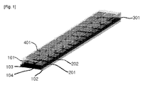
図1は本発明の第1実施例に係る電界放出源を用いた高効率平面型フォトバーを示す斜視図であり、図2は本発明の第1実施例に係る電界放出源を用いた高効率平面型フォトバーを示す断面図である。 FIG. 1 is a perspective view showing a high-efficiency planar photobar using a field emission source according to a first embodiment of the present invention, and FIG. 2 is a high view using a field emission source according to the first embodiment of the present invention. It is sectional drawing which shows an efficiency planar type photobar.
図1および図2に示されるように、本発明の第1実施例に係る電界放出源を用いた高効率平面型フォトバーは、基板102と、基板102上に電極として形成される陰極部202と、陰極部202上に一定の間隔でパターニングされたナノ電界放出源201と、電界放出源201上に絶縁離隔して陰極部202と水平に形成され、電界放出源201からの電子放出を誘導するゲート部301と、ゲート部301上に絶縁離隔して水平に形成され、ターゲット物質401を含む陽極部101とを含んでなる。
As shown in FIGS. 1 and 2, the high efficiency planar photobar using the field emission source according to the first embodiment of the present invention includes a
ここで、陰極部202、ゲート部301および陽極部101が大きく形成される場合、真空に引かれた内部構造物を大気圧から支持するために、基板102と陽極部101との間に基板102および陽極部101に対して垂直に形成される絶縁スペーサ103、104をさらに含むことが可能である。
Here, when the
この際、前記絶縁スペーサ104は基板102とゲート部301との間に位置し、前記絶縁スペーサ103はゲート部301と陽極部101との間に位置する。
At this time, the
また、電界放出源201は、炭素ナノチューブ(CNT)のように内径に対する長さの比が非常に大きいナノワイヤ系の材料を通常適用でき、これにより、好適な例として、CNT(Carbone Nano Tube)、CNF(Carbon Nano Fiber)、CNW(Carbon Nano Wall)、GNF(Graphite Nano Fiber)、グラフェン(Graphene)などのナノカーボン系、ZnO2ナノワイヤ、TiO2ナノワイヤなどの酸化物ナノワイヤ系、TiNナノワイヤなどの窒化物系、タングステンやモリブデン(molybdenum)などの金属系、およびシリコン(silicon:Si)ダイヤモンド(diamond)をコーン形状にエッチングして作ったチップのいずれか1つが使用されることを特徴とする。
In addition, the
前記陽極部101は、ガラス、セラミックおよび金属のいずれか1種の材料からなる基板にターゲット物質が形成されることを特徴とする。
The
次に、上述したように本発明の第1実施例に係る電界放出源を用いた高効率平面型フォトバーの作動原理について説明する。 Next, the operation principle of the high efficiency planar photobar using the field emission source according to the first embodiment of the present invention as described above will be described.
電子放出を誘導するゲート部301に電圧を印加すると、陰極部202上に形成されたナノ電界放出源201に電場(電界)が集中し、これによりナノ電界放出源201から電子501が真空中601に放出される原理を有する。ナノ電界放出源201から放出された電子ビーム501は、絶縁スペーサ103、104を介して特定の距離だけ離隔された陽極部101に到達し、最終的にはX線502に変換されるが、これについての説明を付け加えると、次の通りである。
When a voltage is applied to the
陽極部101は基板にターゲット物質401を形成することで実現可能であり、基板材料および厚さに応じて、図1および図2のようにターゲット(ターゲット物質401)が形成されるべき領域を薄く加工することもできる。本実施例では、陽極部101を形成する基板をガラスと仮定した。ガラス以外に、セラミックや金属などの多様な材料を活用することもできる。
The
本発明の第1実施例に係る図1のような電界放出型フォトバーの場合、陽極部101およびゲート部301にDC電圧を印加した状態で陰極部202に高電圧トランジスタを用いた電流スイッチング駆動が可能であるため、本発明の第1実施例に係るフォトバーは、構造が小さく、その構造により低い電力でも容易に駆動できるという利点がある。
In the case of the field emission type photo bar as shown in FIG. 1 according to the first embodiment of the present invention, a current switching drive using a high voltage transistor for the
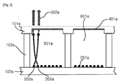
図3は本発明の第2実施例に係る電界放出源を用いた高効率平面型フォトバーを示す断面図である。 FIG. 3 is a sectional view showing a high-efficiency planar photobar using a field emission source according to the second embodiment of the present invention.
図3に示されるように、本発明の第2実施例に係る電界放出源を用いた高効率平面型フォトバーは、基板102aと、基板102a上に多数の電極として分割形成される陰極部202aおよびゲート部203aと、陰極部202aおよびゲート部203a上にパターニングされたナノ電界放出源201aと、陰極部202aおよびゲート部203a上に絶縁離隔して水平に形成され、ターゲット物質401aを含む陽極部101aとを含んでなる。
As shown in FIG. 3, a high-efficiency planar photobar using a field emission source according to the second embodiment of the present invention has a
ここで、陰極部202a、ゲート部203aおよび陽極部101aが大きく形成される場合、真空に引かれた内部構造物を大気圧から支持するために、基板102aと陽極部101aとの間に、基板102aおよび陽極部101aに対して垂直に形成される絶縁スペーサ103aをさらに含むことが可能である。
Here, when the
電界放出源201aは、炭素ナノチューブ(CNT)のように内径に対する長さの比が非常に大きいナノワイヤ系の材料を通常適用でき、これにより、好適な例として、CNT(Carbone Nano Tube)、CNF(Carbon Nano Fiber)、CNW(Carbon Nano Wall)、GNF(Graphite Nano Fiber)、グラフェン(Graphene)などのナノカーボン系材料;ZnO2ナノワイヤ、TiO2ナノワイヤなどの酸化物ナノワイヤ系材料;TiNナノワイヤなどの窒化物系;タングステン、モリブデン(molybdenum)などの金属系;シリコン(silicon:Si);およびダイヤモンド(diamond)をコーン形状にエッチングして作ったチップのいずれか一つが使用されることを特徴とする。
As the
また、陽極部101aは、ガラス、セラミックおよび金属のいずれか1種の材料からなる基板にターゲット物質401aを形成することで実現する。
Moreover, the
次に、上述したように本発明の第2実施例に係る電界放出源を用いた高効率平面型フォトバーの作動原理について説明する。 Next, the operation principle of the high efficiency planar photobar using the field emission source according to the second embodiment of the present invention as described above will be described.
図3は図1および図2のフォトバーと同様の構造において、電子を放出させる電子放出部の構造が変形した形態である。 FIG. 3 shows a configuration in which the structure of the electron emitting portion for emitting electrons is modified in the same structure as the photo bar of FIGS. 1 and 2.
図3の場合、陰極部202aとゲート部203aとが互いに交差しながら駆動する構造であるが、隣接した陰極部202aとゲート部203aとが互いに区別されながら駆動する特性を有する。電極が陰極部202aとして使用されると、隣接する電極はゲート部203aとして使用され、陰極部202aであった電極がゲート部203aとして使用されると、ゲート部203aであった電極が陰極部202aとして使用される構造である。
In the case of FIG. 3, the
この際、図3に示した図面番号501aは電子または電子ビームを示し、502aはX線を示し、601aは真空を示す。
At this time, a
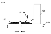
図4は本発明の第3実施例に係る電界放出源を用いた高効率平面型フォトバーを示す断面図である。 FIG. 4 is a sectional view showing a high-efficiency planar photobar using a field emission source according to a third embodiment of the present invention.
図4に示されるように、本発明の第3実施例に係る電界放出源を用いた高効率平面型フォトバーは、基板102bと、基板102b上に多数の電極として互いにナノメートル級の微細なギャップをおいて交互に形成される陰極部202bおよびゲート部203bと、陰極部202bおよびゲート部203b上に絶縁離隔して水平に形成され、ターゲット物質を含む陽極部(図示せず)とから構成される。
As shown in FIG. 4, a high-efficiency planar photobar using a field emission source according to a third embodiment of the present invention has a nanometer-class fineness as a plurality of electrodes on a
この際、陽極部は、本発明の第3実施例に係るフォトバーを示した図4に示されていないが、図2および図3に示した第1実施例および第2実施例に係るフォトバーの陽極部101、101aと同様に構成されることが好ましい。
At this time, the anode portion is not shown in FIG. 4 showing the photo bar according to the third embodiment of the present invention, but the photo according to the first embodiment and the second embodiment shown in FIGS. It is preferable to be configured similarly to the
ここで、陰極部202b、ゲート部301bおよび陽極部が大きく形成される場合、真空に引かれた内部構造物を大気圧から支持するために、基板102aと陽極部との間に基板102aおよび陽極部に対して垂直に形成される絶縁スペーサ103bをさらに含むことが可能である。
Here, when the
次に、上述したように本発明の第3実施例に係る電界放出源を用いた高効率平面型フォトバーの作動原理について説明する。 Next, the operation principle of the high efficiency planar photobar using the field emission source according to the third embodiment of the present invention as described above will be described.
図4は図1〜図3で説明された本発明に係る電界放出型フォトバーの構造において別の方式で適用できる電界放出構造を説明する図である。上述の説明ではナノワイヤおよびナノチップから放出される電子放出構造を示した。一方、図4の場合は、2つの電極を基板102b上に形成させ、両電極間のギャップをナノメートル級の微細隙間として形成させると、ゲート部203bに電圧を印加する場合、陰極部202bから電子がゲート部203bに向かって放出される。この際、放出された電子の一部分がゲート部203bの電極に向かわずに、散乱されて陽極部側に向かう現象が起こり得る構造である。図4の場合も、前記図3の場合と同様に、ゲート部203bと陰極部202bとが互いに交差しながら駆動できる。
FIG. 4 is a diagram illustrating a field emission structure that can be applied in another manner in the structure of the field emission photobar according to the present invention described with reference to FIGS. In the above description, electron emission structures emitted from nanowires and nanotips are shown. On the other hand, in the case of FIG. 4, when two electrodes are formed on the
この際、図4に示した図面番号501bは電子または電子ビームである。
At this time, the drawing
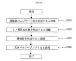
図5は本発明の第1実施例に係る電界放出源を用いた高効率平面型フォトバーの製造方法を示す順序図である。 FIG. 5 is a flow chart showing a method for manufacturing a high-efficiency planar photobar using the field emission source according to the first embodiment of the present invention.
図5に示されるように、本発明の第1実施例に係る電界放出源を用いた高効率平面型フォトバーの製造方法は、基板102上にスクリーン印刷、グラビア印刷、オフセット印刷、インクジェット印刷、フィルム蒸着、または露光および現像方式で陰極部202を形成する(イ)段階(S110)と、陰極部202上にナノ電界放出源201をスクリーン印刷、グラビア印刷、オフセット印刷、インクジェット印刷、フィルム蒸着、または露光および現像方式で形成する(ロ)段階(S120)と、陰極部202上に、一定の間隔の絶縁を確保した離隔をおいてゲート部301を形成する(ハ)段階(S130)と、前記ゲート部301上に、ターゲット物質401を含む陽極部101を形成する(ニ)段階(S140)と、前記(ニ)段階(S140)の後、基板102と陽極部101との間を真空パッケージングする(ホ)段階(S150)とを含んでなることを特徴とする。
As shown in FIG. 5, a method for manufacturing a high-efficiency planar photobar using a field emission source according to the first embodiment of the present invention includes screen printing, gravure printing, offset printing, inkjet printing on a
ここで、陰極部202、ゲート部301および陽極部101が大きく形成される場合、真空に引かれた内部構造物を大気圧から支持するために、基板102と陽極部101との間に垂直に絶縁スペーサ103、104を形成する段階をさらに含むことが可能である。
Here, when the
この際、絶縁スペーサ104は基板102とゲート部301との間に位置し、絶縁スペーサ103はゲート部301と陽極部101との間に位置する。
At this time, the insulating
また、陰極部202は、金属(例えば、Ag、Cu)、酸化物電極材料(例えば、ITO)およびカーボン系電極材料(例えば、グラフェンおよびCNT)のいずれか一つから形成される。
Moreover, the
ナノ電界放出源201は、ペースト、直接成長、スラリー塗布、電気泳動法または浸漬(dipping)のいずれか一つの方式で形成される。
The nano
また、ゲート部301は、金属板をエッチングしてナノ電界放出源201との整列後に配置されるか、ガラス板もしくはセラミック板をエッチングし、一面に電極を形成した後に配置されるか、またはスクリーン印刷法で直接プリントして形成される。
In addition, the
陽極部101は、ゲート部301と高電圧絶縁が保たれる程度に離隔しなければならず、X線を放出させることが可能なターゲット物質401を蒸着、コーティングまたはスクリーン印刷法のいずれか一つの方式で形成される。
The
図6は本発明の第2実施例に係る電界放出源を用いた高効率平面型フォトバーの製造方法を示す順序図である。 FIG. 6 is a flow chart illustrating a method for manufacturing a high efficiency planar photobar using a field emission source according to a second embodiment of the present invention.
図6に示されるように、本発明の第2実施例に係る電界放出源を用いた高効率平面型フォトバーの製造方法は、一定の間隔で基板102a上にスクリーン印刷、グラビア印刷、オフセット印刷、インクジェット印刷、フィルム蒸着、または露光および現像方式で陰極部202aおよびゲート部203aを形成するa段階(S210)と、陰極部202aおよびゲート部203a上にナノ電界放出源201aを形成するb段階(S220)と、陰極部202aおよびゲート部203a上に、ターゲット物質401aを含む陽極部101aを形成するc段階(S230)と、c段階(S230)の後、基板102aと陽極部101aとの間を真空パッケージングするd段階(S240)とから構成される。
As shown in FIG. 6, the method of manufacturing a high efficiency planar photobar using the field emission source according to the second embodiment of the present invention is performed by screen printing, gravure printing, offset printing on a
ここで、陰極部202a、ゲート部203aおよび陽極部101aが大きく形成される場合、真空に引かれた内部構造物を大気圧から支持するために、基板102aと陽極部101aとの間に垂直に絶縁スペーサ103aを形成する段階をさらに含むことが可能である。
Here, when the
陰極部202aは、金属(例えば、Ag、Cu)、酸化物電極材料(例えば、ITO)、およびカーボン系電極材料(例えば、グラフェンおよびCNT)のいずれか一つから形成される。
The
また、ナノ電界放出源201aは、ペースト、直接成長、スラリー塗布、電気泳動法または浸漬(dipping)のいずれか一つの方式で形成される。
The nano
陽極部101aは、ゲート部203aと高電圧絶縁が保たれる程度に離隔しなければならず、X線を放出させることが可能なターゲット物質401aを蒸着、コーティングまたはスクリーン印刷法のいずれか一つの方式で形成される。
The
図7は本発明の第3実施例に係る電界放出源を用いた高効率平面型フォトバーの製造方法を示す順序図である。 FIG. 7 is a flow chart illustrating a method for manufacturing a high efficiency planar photobar using a field emission source according to a third embodiment of the present invention.
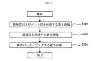
図7に示されるように、本発明の第3実施例に係る電界放出源を用いた高効率フォトバーの製造方法は、基板102b上にスクリーン印刷、グラビア印刷、オフセット印刷、インクジェット印刷、フィルム蒸着、または露光および現像方式で陰極部202bおよびゲート部203bを形成する第1段階(S310)と、基板102b上に、ターゲット物質を含む陽極部を形成する第2段階(S320)と、第2段階(S320)の後、基板102bと陽極部との間を真空パッケージングする第3段階(S330)とから構成される。
As shown in FIG. 7, a method for manufacturing a high-efficiency photobar using a field emission source according to the third embodiment of the present invention includes screen printing, gravure printing, offset printing, inkjet printing, film deposition on a
ここで、陰極部202b、ゲート部203bおよび陽極部が大きく形成される場合、真空に引かれた内部構造物を大気圧から支持するために、基板102bと陽極部との間に垂直に絶縁スペーサ103bを形成する段階をさらに含むことが可能である。
Here, when the
陰極部202bは、金属(例えば、Ag、Cu)、酸化物電極材料(例えば、ITO)、およびカーボン系電極材料(例えば、グラフェンおよびCNT)のいずれか一つで形成される。
The
また、陽極部は、ゲート部203bと高電圧絶縁が保たれる程度に離隔しなければならず、X線を放出させることが可能なターゲット物質を蒸着、コーティングまたはスクリーン印刷法のいずれか一つの方式で形成される。
In addition, the anode part must be separated from the
この際、陽極部は、本発明の第3実施例に係るフォトバーを示した図4に示されていないが、図2および図3に示した第1実施例および第2実施例に係るフォトバーの陽極部101、101aと同様に構成されることが好ましい。
At this time, the anode portion is not shown in FIG. 4 showing the photo bar according to the third embodiment of the present invention, but the photo according to the first embodiment and the second embodiment shown in FIGS. It is preferable to be configured similarly to the
以上説明したように、本発明の詳細な説明では本発明の好適な実施例について説明したが、本発明の属する技術分野における通常の知識を有する者であれば、本発明の範疇から逸脱しない限度内で様々な変形が可能であるのは明白である。よって、本発明の権利範囲は説明された実施例に限定されて定められてはならず、後述する特許請求の範囲、及びこれと均等なものによって定められるべきである。 As described above, the preferred embodiment of the present invention has been described in the detailed description of the present invention. However, those who have ordinary knowledge in the technical field to which the present invention belongs can be used without departing from the scope of the present invention. It is clear that various modifications are possible within. Therefore, the scope of the present invention should not be defined by being limited to the embodiments described, but should be defined by the appended claims and their equivalents.
101、101a 陽極部
102、102a、102b 基板
103、103a、103b、104 絶縁スペーサ
201、201a 電界放出源
202、202a、202b 陰極部
203a、203b、301 ゲート部
401、401a ターゲット物質
501、501a、501b 電子
502、502a X線
601、601a 真空中
101, 101a Anode
Claims (14)
基板と、
前記基板上に電極として形成される陰極部と、
前記陰極部上に一定の間隔でパターニングされた電界放出源と、
前記電界放出源上に絶縁離隔して前記陰極部と水平に形成され、前記電界放出源からの電子放出を誘導するゲート部と、
前記ゲート部上に絶縁離隔して水平に形成され、ターゲット物質を含む陽極部と、を含んでなることを特徴とする、電界放出源を用いた高効率平面型フォトバー。 A high-efficiency planar photobar using a field emission source,
A substrate,
A cathode portion formed as an electrode on the substrate;
A field emission source patterned at regular intervals on the cathode portion;
A gate part that is formed on the field emission source in an insulating manner and horizontally with the cathode part, and induces electron emission from the field emission source;
A high-efficiency planar photobar using a field emission source, comprising: an anode portion that is formed horizontally on the gate portion and is insulated and spaced apart; and a target material.
基板と、
前記基板上に多数の電極として分割形成される陰極部およびゲート部と、
前記陰極部およびゲート部上にパターニングされた電界放出源と、
前記陰極部およびゲート部上に絶縁離隔して水平に形成され、ターゲット物質を含む陽極部と、を含んでなることを特徴とする、電界放出源を用いた高効率平面型フォトバー。 A high-efficiency planar photobar using a field emission source,
A substrate,
A cathode part and a gate part which are divided and formed as a large number of electrodes on the substrate;
A field emission source patterned on the cathode and gate portions;
A high-efficiency planar photobar using a field emission source, comprising: an anode portion that is formed horizontally on the cathode portion and the gate portion and is insulated and spaced apart and includes a target material.
基板と、
前記基板上に多数の電極として互いにナノメートル級の微細なギャップをおいて交互に形成される陰極部およびゲート部と、
前記陰極部およびゲート部上に絶縁離隔して水平に形成され、ターゲット物質を含む陽極部と、を含んでなることを特徴とする、電界放出源を用いた高効率平面型フォトバー。 A high-efficiency planar photobar using a field emission source,
A substrate,
Cathode portions and gate portions that are alternately formed on the substrate as a large number of electrodes with a minute gap of nanometer level, and
A high-efficiency planar photobar using a field emission source, comprising: an anode portion that is formed horizontally on the cathode portion and the gate portion and is insulated and spaced apart and includes a target material.
基板上にスクリーン印刷、グラビア印刷、オフセット印刷、インクジェット印刷、フィルム蒸着、または露光および現像方式で陰極部を形成する(イ)段階と、
前記陰極部上に電界放出源をスクリーン印刷、グラビア印刷、オフセット印刷、インクジェット印刷、フィルム蒸着、または露光および現像方式で形成する(ロ)段階と、
前記陰極部上に、一定の間隔の絶縁を確保した離隔をおいてゲート部を形成する(ハ)段階と、
前記ゲート部上に、ターゲット物質を含む陽極部を形成する(ニ)段階と、
前記(ニ)段階の後、前記基板と前記陽極部との間を真空パッケージングする(ホ)段階とを含んでなることを特徴とする、電界放出源を用いた高効率平面型フォトバーの製造方法。 A method for producing a high-efficiency planar photobar using a field emission source,
(B) forming a cathode portion on the substrate by screen printing, gravure printing, offset printing, inkjet printing, film deposition, or exposure and development;
(B) forming a field emission source on the cathode part by screen printing, gravure printing, offset printing, ink jet printing, film deposition, or exposure and development;
(C) forming a gate part on the cathode part with a separation ensuring insulation at a constant interval;
(D) forming an anode part including a target material on the gate part;
A high-efficiency planar photobar using a field emission source comprising the step (e) of vacuum packaging between the substrate and the anode part after the step (d) Production method.
一定の間隔で基板上にスクリーン印刷、グラビア印刷、オフセット印刷、インクジェット印刷、フィルム蒸着、または露光および現像方式で陰極部およびゲート部を形成するa段階と、
前記陰極部およびゲート部上に電界放出源を形成するb段階と、
前記陰極部およびゲート部上に、ターゲット物質を含む陽極部を形成するc段階と、
前記c段階の後、前記基板と前記陽極部との間を真空パッケージングするd段階とを含んでなることを特徴とする、電界放出源を用いた高効率平面型フォトバーの製造方法。 A method for producing a high-efficiency planar photobar using a field emission source,
A step of forming a cathode portion and a gate portion on a substrate at regular intervals by screen printing, gravure printing, offset printing, ink jet printing, film deposition, or exposure and development;
B-stage forming a field emission source on the cathode and gate portions;
C-stage forming an anode part including a target material on the cathode part and the gate part;
A method of manufacturing a high-efficiency planar photobar using a field emission source, comprising: d step of vacuum packaging between the substrate and the anode part after the c step.
基板上にスクリーン印刷、グラビア印刷、オフセット印刷、インクジェット印刷、フィルム蒸着、または露光および現像方式で陰極部およびゲート部を形成する第1段階と、
前記基板上に、ターゲット物質を含む陽極部を形成する第2段階と、
前記第2段階の後、前記基板と前記陽極部との間を真空パッケージングする第3段階とを含んでなることを特徴とする、電界放出源を用いた高効率平面型フォトバーの製造方法。 A method for producing a high-efficiency planar photobar using a field emission source,
Forming a cathode part and a gate part on a substrate by screen printing, gravure printing, offset printing, ink jet printing, film deposition, or exposure and development;
A second step of forming an anode part including a target material on the substrate;
A method of manufacturing a high-efficiency planar photobar using a field emission source, comprising a third stage of vacuum packaging between the substrate and the anode part after the second stage .
Applications Claiming Priority (3)
| Application Number | Priority Date | Filing Date | Title |
|---|---|---|---|
| KR20110030510 | 2011-04-04 | ||
| KR10-2011-0030510 | 2011-04-04 | ||
| PCT/KR2011/009694 WO2012138041A1 (en) | 2011-04-04 | 2011-12-16 | High-efficient flat type photo bar using field emitter and manufacturing method thereof |
Publications (1)
| Publication Number | Publication Date |
|---|---|
| JP2014502014A true JP2014502014A (en) | 2014-01-23 |
Family
ID=46969403
Family Applications (1)
| Application Number | Title | Priority Date | Filing Date |
|---|---|---|---|
| JP2013539782A Pending JP2014502014A (en) | 2011-04-04 | 2011-12-16 | High-efficiency planar photobar using field emission source and manufacturing method thereof |
Country Status (3)
| Country | Link |
|---|---|
| US (1) | US20140029728A1 (en) |
| JP (1) | JP2014502014A (en) |
| WO (1) | WO2012138041A1 (en) |
Cited By (1)
| Publication number | Priority date | Publication date | Assignee | Title |
|---|---|---|---|---|
| JP2017510052A (en) * | 2014-02-10 | 2017-04-06 | ルクスブライト・アーベー | Electron emitter for X-ray tube |
Families Citing this family (2)
| Publication number | Priority date | Publication date | Assignee | Title |
|---|---|---|---|---|
| US20180013869A1 (en) * | 2016-07-07 | 2018-01-11 | Vladimir Smelyansky | Integration of voip phone services with intelligent cloud voice recognition |
| US10848001B2 (en) * | 2017-07-27 | 2020-11-24 | Garrity Power Services Llc | Thin film photovoltaic wireless interface |
Citations (13)
| Publication number | Priority date | Publication date | Assignee | Title |
|---|---|---|---|---|
| JPS6486427A (en) * | 1987-02-06 | 1989-03-31 | Canon Kk | Multi-type electron emission element and manufacture thereof |
| US5361015A (en) * | 1987-02-06 | 1994-11-01 | Canon Kabushiki Kaisha | Electron emission element |
| JPH11135004A (en) * | 1997-10-28 | 1999-05-21 | Nippon Hoso Kyokai <Nhk> | Diamond cold cathode manufacturing device |
| JP2003507873A (en) * | 1999-08-21 | 2003-02-25 | プリンタブル フィールド エミッターズ リミテッド | Field emitters and devices |
| US20050074093A1 (en) * | 2003-10-03 | 2005-04-07 | Johann Kindlein | Solid state bracytherapy applicator |
| JP2006156377A (en) * | 2004-12-01 | 2006-06-15 | Nanopacific Inc | Field emission device driven by bipolar pulse power supply |
| JP2006209982A (en) * | 2005-01-25 | 2006-08-10 | Seiko Epson Corp | Electron emitting element, its manufacturing method, and electro-optical device, and electronic equipment |
| JP2006527459A (en) * | 2003-06-06 | 2006-11-30 | エレクトロバック ファブリカツィオン エレクトロテクニッシャー スペツィアラールティケル ゲーエムベーハー | Electron emitter and manufacturing process |
| JP2007311186A (en) * | 2006-05-18 | 2007-11-29 | Hamamatsu Photonics Kk | X-ray tube |
| JP2008507096A (en) * | 2004-07-14 | 2008-03-06 | ザ ボード オブ トラスティーズ オブ ザ ユニバーシティ オブ イリノイ | Microdischarge device assisted by field emission |
| JP2008251341A (en) * | 2007-03-30 | 2008-10-16 | Nagaoka Univ Of Technology | X-ray generator |
| JP2009205992A (en) * | 2008-02-28 | 2009-09-10 | Canon Inc | Multi x-ray generator and radiographic equipment |
| JP2010086966A (en) * | 2008-09-30 | 2010-04-15 | Samsung Electronics Co Ltd | Composition for electron emission source formation, electron emission source formed using this, its manufacturing method, and field emission element using this |
Family Cites Families (8)
| Publication number | Priority date | Publication date | Assignee | Title |
|---|---|---|---|---|
| US5204891A (en) * | 1991-10-30 | 1993-04-20 | General Electric Company | Focal track structures for X-ray anodes and method of preparation thereof |
| JP3647436B2 (en) * | 2001-12-25 | 2005-05-11 | キヤノン株式会社 | Electron-emitting device, electron source, image display device, and method for manufacturing electron-emitting device |
| US6560315B1 (en) * | 2002-05-10 | 2003-05-06 | Ge Medical Systems Global Technology Company, Llc | Thin rotating plate target for X-ray tube |
| KR100699799B1 (en) * | 2004-12-01 | 2007-03-27 | 나노퍼시픽(주) | Field emision device derived by bipolar pulse |
| WO2006130630A2 (en) * | 2005-05-31 | 2006-12-07 | The University Of North Carolina At Chapel Hill | X-ray pixel beam array systems and methods for electronically shaping radiation fields and modulating radiation field intensity patterns for radiotherapy |
| KR101100816B1 (en) * | 2005-07-29 | 2012-01-02 | 삼성에스디아이 주식회사 | Electron emission source for emitting thermal electron, electron emission device having the same, flat display apparatus having the same, and method of manufacturing the same |
| KR101281168B1 (en) * | 2007-01-05 | 2013-07-02 | 삼성전자주식회사 | Field emission electrode, method for preparing the same and field emission device comprising the same |
| KR100934817B1 (en) * | 2007-11-15 | 2009-12-31 | 경희대학교 산학협력단 | Actively Driven X-ray Lamps and Manufacturing Method Thereof |
-
2011
- 2011-12-16 WO PCT/KR2011/009694 patent/WO2012138041A1/en active Application Filing
- 2011-12-16 JP JP2013539782A patent/JP2014502014A/en active Pending
- 2011-12-16 US US13/988,489 patent/US20140029728A1/en not_active Abandoned
Patent Citations (16)
| Publication number | Priority date | Publication date | Assignee | Title |
|---|---|---|---|---|
| US5361015A (en) * | 1987-02-06 | 1994-11-01 | Canon Kabushiki Kaisha | Electron emission element |
| JPS6486427A (en) * | 1987-02-06 | 1989-03-31 | Canon Kk | Multi-type electron emission element and manufacture thereof |
| JPH11135004A (en) * | 1997-10-28 | 1999-05-21 | Nippon Hoso Kyokai <Nhk> | Diamond cold cathode manufacturing device |
| JP2003507873A (en) * | 1999-08-21 | 2003-02-25 | プリンタブル フィールド エミッターズ リミテッド | Field emitters and devices |
| US20040198132A1 (en) * | 1999-08-21 | 2004-10-07 | Tuck Richard Allan | Field emitters and devices |
| JP2006527459A (en) * | 2003-06-06 | 2006-11-30 | エレクトロバック ファブリカツィオン エレクトロテクニッシャー スペツィアラールティケル ゲーエムベーハー | Electron emitter and manufacturing process |
| US20050074093A1 (en) * | 2003-10-03 | 2005-04-07 | Johann Kindlein | Solid state bracytherapy applicator |
| JP2005111252A (en) * | 2003-10-03 | 2005-04-28 | Nucletron Bv | Solid state brachytherapy applicator |
| JP2008507096A (en) * | 2004-07-14 | 2008-03-06 | ザ ボード オブ トラスティーズ オブ ザ ユニバーシティ オブ イリノイ | Microdischarge device assisted by field emission |
| JP2006156377A (en) * | 2004-12-01 | 2006-06-15 | Nanopacific Inc | Field emission device driven by bipolar pulse power supply |
| JP2006209982A (en) * | 2005-01-25 | 2006-08-10 | Seiko Epson Corp | Electron emitting element, its manufacturing method, and electro-optical device, and electronic equipment |
| JP2007311186A (en) * | 2006-05-18 | 2007-11-29 | Hamamatsu Photonics Kk | X-ray tube |
| JP2008251341A (en) * | 2007-03-30 | 2008-10-16 | Nagaoka Univ Of Technology | X-ray generator |
| JP2009205992A (en) * | 2008-02-28 | 2009-09-10 | Canon Inc | Multi x-ray generator and radiographic equipment |
| US20090232270A1 (en) * | 2008-02-28 | 2009-09-17 | Canon Kabushiki Kaisha | Multi x-ray generating apparatus and x-ray imaging apparatus |
| JP2010086966A (en) * | 2008-09-30 | 2010-04-15 | Samsung Electronics Co Ltd | Composition for electron emission source formation, electron emission source formed using this, its manufacturing method, and field emission element using this |
Cited By (2)
| Publication number | Priority date | Publication date | Assignee | Title |
|---|---|---|---|---|
| JP2017510052A (en) * | 2014-02-10 | 2017-04-06 | ルクスブライト・アーベー | Electron emitter for X-ray tube |
| US10825635B2 (en) | 2014-02-10 | 2020-11-03 | Luxbright Ab | Electron emitter for an x-ray tube |
Also Published As
| Publication number | Publication date |
|---|---|
| US20140029728A1 (en) | 2014-01-30 |
| WO2012138041A1 (en) | 2012-10-11 |
Similar Documents
| Publication | Publication Date | Title |
|---|---|---|
| US7652418B2 (en) | Electronic emission device, electron emission display device having the same, and method of manufacturing the electron emission device | |
| TWI550675B (en) | Electron emission device and electron emission display | |
| TWI550677B (en) | Electron emission source | |
| TWI529771B (en) | Electron emission device and display | |
| TWI534846B (en) | Electron emission device and display | |
| JP2009231289A (en) | Field emission display device | |
| JP2008091324A (en) | Electron emitter and display apparatus utilizing the same | |
| TW201530601A (en) | Electron emission source | |
| JP2004178891A (en) | Manufacturing method of electron emitting type light emitting device | |
| JP2014502014A (en) | High-efficiency planar photobar using field emission source and manufacturing method thereof | |
| JP2004253201A (en) | Field emission type cold cathode and its manufacturing method | |
| KR101082440B1 (en) | Electron emission device, electron emission display apparatus having the same, and method of manufacturing the same | |
| JP2001043792A (en) | Manufacture of electron emitting source, electron emitting source, and fluorescent light emitting type display | |
| JP2004241161A (en) | Electron emitting source and its manufacturing method and its display device | |
| JP5332745B2 (en) | Light emitting device | |
| JP2000294119A (en) | Manufacture of electron emission source, electron emission source and fluorescent light display | |
| TWI386966B (en) | Field emission display | |
| KR20060114865A (en) | Electron emitting element, and method of manufacturing the same | |
| TWI330858B (en) | Thermionic emission device | |
| KR20100012573A (en) | Field emission device using carbon nanotubes of and method of the same | |
| KR100898071B1 (en) | Electron emission device, electron emission display apparatus having the same, and method of manufacturing the same | |
| JP2000340100A (en) | Manufacture of electron emission source, electron emission source and fluorescent light emission type indicator | |
| JP4043141B2 (en) | Method for manufacturing electron emission source and electron emission source | |
| TWI383420B (en) | Electron emitter and displaying device using the same | |
| JP2008226825A (en) | Electron emission device, electron emission display device equipped with it, and its manufacturing method |
Legal Events
| Date | Code | Title | Description |
|---|---|---|---|
| A977 | Report on retrieval |
Free format text: JAPANESE INTERMEDIATE CODE: A971007 Effective date: 20140523 |
|
| A131 | Notification of reasons for refusal |
Free format text: JAPANESE INTERMEDIATE CODE: A131 Effective date: 20140602 |
|
| A521 | Request for written amendment filed |
Free format text: JAPANESE INTERMEDIATE CODE: A523 Effective date: 20140827 |
|
| A02 | Decision of refusal |
Free format text: JAPANESE INTERMEDIATE CODE: A02 Effective date: 20150202 |