JP2014236373A - A/d conversion device - Google Patents

A/d conversion device Download PDF

Info

Publication number
JP2014236373A
JP2014236373A JP2013116859A JP2013116859A JP2014236373A JP 2014236373 A JP2014236373 A JP 2014236373A JP 2013116859 A JP2013116859 A JP 2013116859A JP 2013116859 A JP2013116859 A JP 2013116859A JP 2014236373 A JP2014236373 A JP 2014236373A
Authority
JP
Japan
Prior art keywords
conversion
converter
flash
circuit
bits
Prior art date
Legal status (The legal status is an assumption and is not a legal conclusion. Google has not performed a legal analysis and makes no representation as to the accuracy of the status listed.)
Pending
Application number
JP2013116859A
Other languages
Japanese (ja)
Inventor
日比 康博
Yasuhiro Hibi
康博 日比
原田 卓哉
Takuya Harada
卓哉 原田
Current Assignee (The listed assignees may be inaccurate. Google has not performed a legal analysis and makes no representation or warranty as to the accuracy of the list.)
Denso Corp
Original Assignee
Denso Corp
Priority date (The priority date is an assumption and is not a legal conclusion. Google has not performed a legal analysis and makes no representation as to the accuracy of the date listed.)
Filing date
Publication date
Application filed by Denso Corp filed Critical Denso Corp
Priority to JP2013116859A priority Critical patent/JP2014236373A/en
Publication of JP2014236373A publication Critical patent/JP2014236373A/en
Pending legal-status Critical Current

Links

Images

Abstract

PROBLEM TO BE SOLVED: To provide an A/D conversion device that produces an A/D conversion value at high speed and with high precision even if an RC time constant has an effect in a configuration using a capacitor array D/A converter.SOLUTION: A flash A/D converter 2 performs a flash A/D conversion processing on an analog signal to tentatively decide upper x bits. A successive conversion section 3, on the other hand, stores an electrical charge in a capacitor array and successively compares an analog output value to A/D-convert a sampling value. The successive conversion section 3 applies a redundant algorithm repeating the successive conversion n-x+α times as using the result of the A/D conversion processing of the upper x bits by the flash A/D converter 2, to perform an A/D conversion processing of lower n-x bits. This can ensure an A/D conversion value to handle a higher precision A/D conversion processing.

Description

本発明は、アナログ信号をデジタル値にA/D変換処理するA/D変換装置に関する。   The present invention relates to an A / D conversion apparatus that performs A / D conversion processing on an analog signal into a digital value.

この種のA/D変換装置は、高速動作可能で且つ精度を向上することが求められている。このような逐次比較型A/D変換回路が特許文献1に開示されている。この特許文献1記載の逐次比較型のA/D変換回路によれば、コンパレータがアナログ入力電圧と、複数の比較電圧のそれぞれとを比較しこの並列比較を逐次行っている。   This type of A / D converter is required to operate at high speed and to improve accuracy. Such a successive approximation type A / D conversion circuit is disclosed in Patent Document 1. According to the successive approximation A / D conversion circuit described in Patent Document 1, the comparator compares the analog input voltage with each of the plurality of comparison voltages, and sequentially performs the parallel comparison.

逐次比較レジスタは、並列比較の結果が得られると、並列比較の結果に基いて、前回の所定のサーチ電圧範囲内において、次回の所定のサーチ電圧範囲を設定し、D/Aコンバータにデジタル値を逐次与える。そして、タイミング制御回路は、所定のタイミングで並列比較から冗長比較への切り替えを行うための信号を生成する。これにより、コンパレータが並列比較を逐次行うので高速変換できる。   When the result of the parallel comparison is obtained, the successive approximation register sets the next predetermined search voltage range within the previous predetermined search voltage range based on the result of the parallel comparison, and outputs a digital value to the D / A converter. Are given sequentially. Then, the timing control circuit generates a signal for switching from parallel comparison to redundant comparison at a predetermined timing. Thereby, since the comparator sequentially performs parallel comparison, high-speed conversion can be performed.

特開2009−302716号公報JP 2009-302716 A

逐次比較型のA/D変換装置は容量アレイを備えた容量アレイ型D/A変換回路を備えて構成される。容量アレイ型D/A変換回路は容量アレイに抵抗成分を有する。すると、この容量アレイ型D/A変換回路は、電荷再分配時のRC時定数に応じて各ビットを定めるための処理時間が決定される。すなわち、この種のA/D変換装置は、このRC時定数の影響から電荷再分配に時間を要することから各ビットの決定に時間を要し高速化に限界を生じる。   The successive approximation A / D converter includes a capacitor array D / A converter circuit including a capacitor array. The capacitance array type D / A conversion circuit has a resistance component in the capacitance array. Then, in this capacitor array type D / A conversion circuit, the processing time for determining each bit is determined according to the RC time constant at the time of charge redistribution. In other words, this type of A / D converter requires time for charge redistribution due to the influence of the RC time constant, so that it takes time to determine each bit and limits speeding up.

本発明の目的は、高速で且つ高精度にA/D変換値を得られるようにしたA/D変換装置を提供することにある。   An object of the present invention is to provide an A / D conversion apparatus that can obtain an A / D conversion value at high speed and with high accuracy.

請求項1記載の発明は、アナログ信号をサンプリングしnビットのデジタル値にA/D変換処理するA/D変換装置を対象としている。この請求項1記載の発明によれば、フラッシュA/D変換部は、アナログ信号をフラッシュA/D変換処理し上位xビットを決定する。他方、逐次比較部はサンプリング値を容量アレイ型D/A変換部のアナログ出力値と逐次比較する。逐次比較部の容量アレイ型D/A変換部はサンプリング値を電荷再分配する間に時間を要するものの、この電荷再分配処理するまでの間に、フラッシュA/D変換部が上位xビットをA/D変換しているため並列処理できる。したがって逐次変換部によるサンプリング時間を短縮できる。   The first aspect of the present invention is directed to an A / D conversion apparatus that samples an analog signal and performs A / D conversion processing to an n-bit digital value. According to the first aspect of the present invention, the flash A / D conversion unit performs flash A / D conversion processing on the analog signal to determine the upper x bits. On the other hand, the successive approximation unit sequentially compares the sampling value with the analog output value of the capacitance array type D / A conversion unit. Although the capacity array type D / A conversion unit of the successive approximation unit requires time to redistribute the sampling value, the flash A / D conversion unit converts the upper x bits into A before the charge redistribution processing is performed. Parallel processing is possible due to / D conversion. Therefore, the sampling time by the successive approximation unit can be shortened.

逐次変換部は、フラッシュA/D変換部が上位xビットをA/D変換処理した結果を用いて逐次変換し上位xビットと共に下位n−xビットをA/D変換処理する。これにより、A/D変換処理を高速化しつつA/D変換精度を高精度化できる。しかも、逐次変換部はn−x+α回逐次変換を繰り返した冗長アルゴリズムを適用して下位n−xビットをA/D変換処理するため、A/D変換値を担保できA/D変換処理をより高精度に処理できる。   The sequential conversion unit sequentially converts the result of the A / D conversion processing of the upper x bits by the flash A / D conversion unit, and performs A / D conversion processing of the lower nx bits together with the upper x bits. Thereby, the A / D conversion accuracy can be increased while the A / D conversion processing is speeded up. In addition, since the successive conversion unit applies a redundant algorithm in which nx + α sequential conversions are repeated to perform A / D conversion processing on the lower nx bits, the A / D conversion value can be secured and the A / D conversion processing can be further performed. Can be processed with high accuracy.

第1実施形態に係るA/D変換装置を概略的に示す電気的構成図1 is an electrical configuration diagram schematically showing an A / D conversion device according to a first embodiment. サンプルホールド回路及びD/A変換器の回路構成例(その1)Sample configuration of sample hold circuit and D / A converter (part 1) サンプルホールド回路及びD/A変換器の回路構成例(その2)Sample configuration of sample hold circuit and D / A converter (part 2) サンプルホールド回路及びD/A変換器の回路構成例(その3)Sample configuration of sample hold circuit and D / A converter (part 3) チョッパコンパレータの回路構成例Circuit configuration example of chopper comparator 非2進アルゴリズム実行回路の構成例Non-binary algorithm execution circuit configuration example 制御信号生成回路の構成例Configuration example of control signal generation circuit 論理回路の真理値表Truth table of logic circuit マルチプレクサの回路構成例Example of multiplexer circuit configuration D/A変換制御レジスタの構成例Configuration example of D / A conversion control register A/D変換値格納レジスタの構成例Configuration example of A / D conversion value storage register A/D変換処理の流れを示すタイミングチャートTiming chart showing the flow of A / D conversion processing 比較ステップに応じた処理結果および許容誤差の説明図Explanatory drawing of processing results and tolerances according to comparison steps A/D変換処理の流れの変形例を示すタイミングチャートTiming chart showing a modified example of the flow of A / D conversion processing 第2実施形態に係るA/D変換装置を概略的に示す電気的構成図(図1相当図)Electrical configuration diagram schematically showing the A / D converter according to the second embodiment (corresponding to FIG. 1) A/D変換処理の流れを概略的に示すタイミングチャート(その1)Timing chart schematically showing the flow of A / D conversion processing (part 1) A/D変換処理の流れを概略的に示すタイミングチャート(その2)Timing chart schematically showing the flow of A / D conversion processing (part 2) 本発明の第3実施形態に係るA/D変換装置を概略的に示す電気的構成図Electrical configuration diagram schematically showing an A / D converter according to a third embodiment of the present invention A/D変換処理の流れを概略的に示すタイミングチャート(図16、図17相当図)Timing chart schematically showing the flow of the A / D conversion process (corresponding to FIGS. 16 and 17) 第4実施形態に係るA/D変換装置を概略的に示す電気的構成図Electrical configuration diagram schematically showing an A / D converter according to a fourth embodiment A/D変換処理の流れを概略的に示すタイミングチャート(図16、図17相当図)Timing chart schematically showing the flow of the A / D conversion process (corresponding to FIGS. 16 and 17)

以下では幾つかの実施形態を説明する。各実施形態の構成要素が同一又は類似部分については同一又は類似符号を付して説明を必要に応じて省略し、以下では各実施形態の特徴部分を中心に説明する。   Several embodiments are described below. Components having the same or similar components in each embodiment are denoted by the same or similar reference numerals, and description thereof is omitted as necessary. Hereinafter, characteristic portions of each embodiment will be mainly described.

(第1実施形態)
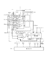
図1にnビットA/D変換装置1のブロック構成を示すように、A/D変換装置1は、上位mビットのフラッシュ型のA/D変換器(フラッシュA/D変換部相当)2と、逐次比較型のA/D変換器(逐次変換部相当)3とを備え、全体を統括制御する制御回路4を接続して構成される。制御回路4は、例えばロジック回路などを用いて構成され、逐次変換部3にA/Dスタート信号を出力すると共にクロックCLKを供給し、A/D変換処理のタイミングを決定する。
(First embodiment)
As shown in the block configuration of the n-bit A / D converter 1 in FIG. 1, the A / D converter 1 includes an upper m-bit flash A / D converter (corresponding to a flash A / D converter) 2. And a successive approximation type A / D converter (corresponding to a successive conversion unit) 3 and connected to a control circuit 4 for overall control. The control circuit 4 is configured using, for example, a logic circuit, and outputs an A / D start signal to the sequential conversion unit 3 and supplies a clock CLK to determine the timing of A / D conversion processing.

フラッシュA/D変換器2は、参照信号を出力する抵抗ラダー回路5と、2−1個のコンパレータ6と、バイナリエンコーダ7とを備える。抵抗ラダー回路5は、第1参照電圧Vref+の供給端子と第2参照電圧Vref-(例えばグランド)の供給端子との間に接続されており、抵抗ラダー回路5による2−1個の分圧電圧をコンパレータ6に参照電圧として出力する。 The flash A / D converter 2 includes a resistance ladder circuit 5 that outputs a reference signal, 2 n −1 comparators 6, and a binary encoder 7. The resistance ladder circuit 5 is connected between the supply terminal of the first reference voltage Vref + and the supply terminal of the second reference voltage Vref− (for example, ground), and 2 n −1 divided by the resistance ladder circuit 5. The voltage is output to the comparator 6 as a reference voltage.

−1個のコンパレータ6は、抵抗ラダー回路5の2−1個の分圧電圧をそれぞれ比較対象電圧として入力する。それぞれのコンパレータ6は、アナログ入力電圧Vinと比較対象電圧とを大小比較し「1」(=「H」)または「0」(=「L」)を出力する。このように、コンパレータ6は2−1個並列に処理することで測定速度およびその分解能を高めることができる。バイナリエンコーダ7は、各コンパレータ6の出力をコード変換しnビットのA/D変換結果を得るが、このうち上位xビット(例えば3ビット<n)を逐次変換部3に出力する。 The 2 n -1 comparators 6 respectively input 2 n -1 divided voltages of the resistance ladder circuit 5 as comparison target voltages. Each comparator 6 compares the analog input voltage Vin with the voltage to be compared and outputs “1” (= “H”) or “0” (= “L”). Thus, the comparator 6 can increase the measurement speed and its resolution by processing 2 n -1 in parallel. The binary encoder 7 performs code conversion on the output of each comparator 6 to obtain an n-bit A / D conversion result, and outputs the upper x bits (for example, 3 bits <n) to the sequential conversion unit 3.

逐次変換部3は、nビット中の下位n−xビットの量子化デジタルデータを主に算出し、フラッシュA/D変換器2が出力する上位xビットのデジタルデータを用いて全nビットの量子化デジタルデータを出力する。この逐次変換部3は、サンプルホールド回路8と、チョッパ型のコンパレータ9と、nビットのD/A変換器10と、非2進アルゴリズム実行回路(冗長アルゴリズム実行回路)11とを備える。   The successive approximation unit 3 mainly calculates lower nx-bit quantized digital data in n bits, and uses all higher-bit digital data output from the flash A / D converter 2 to generate all n-bit quantum data. Output digitized digital data. The successive approximation unit 3 includes a sample-and-hold circuit 8, a chopper comparator 9, an n-bit D / A converter 10, and a non-binary algorithm execution circuit (redundant algorithm execution circuit) 11.

図2はサンプルホールド回路8及びD/A変換器10の構成例を示す。D/A変換器10は、所謂容量アレイD/A変換器により構成され、n+1個のコンデンサC1〜Cn+1、n+1個のスイッチSW1〜SWn+1を組み合わせて構成されている。   FIG. 2 shows a configuration example of the sample hold circuit 8 and the D / A converter 10. The D / A converter 10 is configured by a so-called capacitance array D / A converter, and is configured by combining n + 1 capacitors C1 to Cn + 1 and n + 1 switches SW1 to SWn + 1.

また、サンプルホールド回路8はサンプルホールドスイッチSWHを備える。サンプルホールド回路8は、スイッチ切換制御信号SWsmpが「L」の間にサンプルホールドスイッチSWHを入力電圧Vinの端子側に切換え、スイッチ切換制御信号SWsmpが「H」になるとサンプルホールドスイッチSWHをVref+側に切換えてサンプルホールドする。D/A変換器10は、nビットデータが与えられると、このnビットデータに応じて各スイッチSW1〜SWn+1を切換え、容量アレイコンデンサC1〜Cn+1の蓄積電荷を再分配する。   The sample hold circuit 8 includes a sample hold switch SWH. The sample hold circuit 8 switches the sample hold switch SWH to the terminal side of the input voltage Vin while the switch change control signal SWsmp is “L”, and when the switch change control signal SWsmp becomes “H”, the sample hold switch SWH is changed to the Vref + side. Switch to and hold the sample. When n-bit data is given, the D / A converter 10 switches the switches SW1 to SWn + 1 in accordance with the n-bit data and redistributes the accumulated charges of the capacitor array capacitors C1 to Cn + 1.

図3はサンプルホールド回路8及びD/A変換器110の他の構成例を示す。このD/A変換器110は図1のD/A変換器10に代えて構成しても良い。D/A変換器110は、上位n1ビットのD/A変換部110n1と、下位n2ビットのD/A変換部110n2を組み合わせて構成されている。上位のD/A変換部110n1は、容量比が図示(例えば0.5C:0.5C:C:…:2C)のコンデンサCN11、CN12、CN13…と、切換スイッチSWN11、SWN12、SWN13…とを図示形態に組み合わせて構成される。下位のD/A変換部110n2は、容量比が図示(例えばC:C:2C:…:2n−1C)のコンデンサCN21、CN22、CN23…と、切換スイッチSWN21、SWN22、SWN23…とを図示形態に組み合わせて構成されている。 FIG. 3 shows another configuration example of the sample hold circuit 8 and the D / A converter 110. The D / A converter 110 may be configured in place of the D / A converter 10 of FIG. The D / A converter 110 is configured by combining an upper n1 bit D / A converter 110n1 and a lower n2 bit D / A converter 110n2. The high-order D / A converter 110n1 includes capacitors CN11, CN12, CN13... With changeover switches SWN11, SWN12, SWN13... Whose capacitance ratio is shown (for example, 0.5C: 0.5C: C:... 2C). It is configured in combination with the illustrated form. The low-order D / A converter 110n2 includes capacitors CN21, CN22, CN23... And capacitance switches SWN21, SWN22, SWN23... Whose capacitance ratio is shown in the figure (for example, C: C: 2C:... 2n-1 C). It is configured in combination with the illustrated form.

サンプリングノードSNにはサンプルホールドスイッチSWHを介して入力電圧Vinが入力される。また、D/A変換器110内にはD/A変換部110n1および110n2を初期状態から動作させるためのスイッチSdが設けられる。リセット時には、例えば非2進アルゴリズム実行回路11は、スイッチSdを抵抗分圧回路12の分圧電圧側に切換制御し、実動作時にはサンプリングノードSN側に切換制御しサンプリングノードSNに入力電圧Vinを入力して動作させる。   The input voltage Vin is input to the sampling node SN via the sample hold switch SWH. The D / A converter 110 is provided with a switch Sd for operating the D / A converters 110n1 and 110n2 from the initial state. At the time of resetting, for example, the non-binary algorithm execution circuit 11 switches the switch Sd to the divided voltage side of the resistance voltage dividing circuit 12, and switches to the sampling node SN side at the time of actual operation and applies the input voltage Vin to the sampling node SN. Enter and operate.

このD/A変換器110は、下位側のD/A変換部110n2に下位n2ビットのデータが与えられると、このデータに応じて電荷を再分配し容量アレイの出力ノードの電位を決定する。そして上位側のD/A変換部10n1は上位n1ビットデータが与えられると、このn1ビットデータに応じて電荷を再分配し上位側の容量アレイの出力ノードのCアレイを出力する。   When the low-order n2 bit data is given to the low-order D / A conversion section 110n2, the D / A converter 110 redistributes the charge according to this data and determines the potential of the output node of the capacitor array. When the upper n1 bit data is given, the upper D / A converter 10n1 redistributes the charge according to the n1 bit data and outputs the C array of the output node of the upper capacitor array.

図4はサンプルホールド回路8及びD/A変換器210の他の構成例を示す。このD/A変換器210は図1のD/A変換器10に代えて構成しても良い。このD/A変換器210は、上位n1ビットのD/A変換部210n1と、下位n2ビットのD/A変換部210n2とを組み合わせて構成されている。   FIG. 4 shows another configuration example of the sample hold circuit 8 and the D / A converter 210. The D / A converter 210 may be configured in place of the D / A converter 10 of FIG. This D / A converter 210 is configured by combining an upper n1 bit D / A converter 210n1 and a lower n2 bit D / A converter 210n2.

図4に示す下位のD/A変換部210n2は、ラダー抵抗15と、スイッチ及びデコーダ16を従属接続した抵抗ラダー型のD/A変換器により構成される。また上位のD/A変換部210n1は、D/A変換部110n1と同一構成の容量アレイ型のD/A変換器により構成される。このD/A変換器210は、下位側のD/A変換部210n2に下位n2ビットデータが与えられると、このn2ビットデータに応じてラダー抵抗15で分圧された分圧電圧を切換出力すると共にデコードしアナログ出力電位を上位のD/A変換部210n1に出力する。そして、上位n1ビットの信号データが上位のD/A変換部210n1に与えられると、容量アレイ型のD/A変換部210n1はこのn1ビットデータに応じて電荷再分配し、上位の出力ノードの電位を決定する。図1のD/A変換器10としては、図2〜図4の何れのD/A変換器10、110、210を用いても良いが、以下では、図2に示すD/A変換器10の構成を用いて実施形態を説明する。   The low-order D / A converter 210n2 shown in FIG. 4 includes a ladder resistor 15 and a resistor ladder type D / A converter in which a switch and a decoder 16 are cascade-connected. The upper D / A converter 210n1 is composed of a capacitance array type D / A converter having the same configuration as the D / A converter 110n1. When the lower n2 bit data is given to the lower D / A converter 210n2, the D / A converter 210 switches and outputs the divided voltage divided by the ladder resistor 15 in accordance with the n2 bit data. At the same time, it decodes and outputs the analog output potential to the upper D / A converter 210n1. When the upper n1 bit signal data is supplied to the upper D / A converter 210n1, the capacitance array type D / A converter 210n1 redistributes the charge according to the n1 bit data, and the upper output node Determine the potential. As the D / A converter 10 in FIG. 1, any of the D / A converters 10, 110, and 210 in FIGS. 2 to 4 may be used, but in the following, the D / A converter 10 shown in FIG. The embodiment will be described using the configuration.

図5はチョッパコンパレータ9の構成例を示す。このチョッパコンパレータ9は、サンプリング値を波形整形するバッファ17と、このバッファ17の出力電圧とD/A変換器10の変換出力電圧とを比較するコンパレータ18、19とを備える。コンパレータ18、19は従属接続されている。これらのコンパレータ18および19間にはDCカット用のコンデンサ20および21が設けられている。   FIG. 5 shows a configuration example of the chopper comparator 9. The chopper comparator 9 includes a buffer 17 that shapes the sampling value, and comparators 18 and 19 that compare the output voltage of the buffer 17 with the converted output voltage of the D / A converter 10. The comparators 18 and 19 are connected in cascade. Between these comparators 18 and 19, capacitors 20 and 21 for DC cut are provided.

チョッパコンパレータ9は、D/A変換器10の変換値とサンプリング値を比較しこの比較結果を出力する。なお、各コンパレータ18、19の入力端子間には、それぞれ初期化用のスイッチ22b、22aが設けられており、A/Dスタートタイミング(後述するSWa→「H」、SWb→「H」)において、コンパレータ18の入力端子電位を一致させると共に、コンパレータ19の各入力端子の電位をサンプリング値出力に一致させるように構成されている。   The chopper comparator 9 compares the converted value of the D / A converter 10 with the sampling value and outputs the comparison result. Note that initialization switches 22b and 22a are provided between the input terminals of the comparators 18 and 19, respectively. At an A / D start timing (SWa → “H”, SWb → “H” described later), The input terminal potential of the comparator 18 is matched, and the potential of each input terminal of the comparator 19 is matched with the sampling value output.

図6に非2進アルゴリズム実行回路11の内部回路構成例を示すように、非2進アルゴリズム実行回路11は、シーケンサ加減算値を算出するための制御信号生成回路23と、マルチプレクサ24と、加算器25と、減算器26と、D/A変換制御レジスタ27と、A/D変換値格納レジスタ28と、を備える。   As shown in the internal circuit configuration example of the non-binary algorithm execution circuit 11 in FIG. 6, the non-binary algorithm execution circuit 11 includes a control signal generation circuit 23 for calculating a sequencer addition / subtraction value, a multiplexer 24, and an adder. 25, a subtractor 26, a D / A conversion control register 27, and an A / D conversion value storage register 28.

図7(A),図7(B)に制御信号生成回路23の構成例を示す。また図8に各回路の遷移状態と論理回路の真理値表を示す。図7(A),図7(B)に示すように、制御信号生成回路23は、シフトレジスタ29と、NORゲート30と、NOTゲート31〜33と、イネーブル端子付きDフリップフロップ34と、ADENDパルス生成回路35とを備える。図7(C)はイネーブル端子付きDフリップフロップ34の等価回路を示す。このDフリップフロップ34は、そのイネーブル端子ENが「H」のときにD入力をQ出力とし、イネーブル端子ENが「L」のときにD入力をQ出力に一致させる。   7A and 7B show a configuration example of the control signal generation circuit 23. FIG. FIG. 8 shows a transition state of each circuit and a truth table of the logic circuit. As shown in FIGS. 7A and 7B, the control signal generation circuit 23 includes a shift register 29, a NOR gate 30, NOT gates 31 to 33, a D flip-flop 34 with an enable terminal, and ADEND. And a pulse generation circuit 35. FIG. 7C shows an equivalent circuit of the D flip-flop 34 with an enable terminal. The D flip-flop 34 sets the D input to the Q output when the enable terminal EN is “H”, and matches the D input to the Q output when the enable terminal EN is “L”.

図7(A)に示すように、シフトレジスタ29は例えば5ビット構成である。NORゲート30はこのシフトレジスタ29の上位2ビットのQ4、Q5出力を否定論理和演算し、この結果を最下位ビットのD入力に与える。クロックCLKがNOTゲート31、32を介してクロック端子Cに与えられると、図8に示すように、シフトレジスタ29は、
(Q1,Q2,Q3,Q4,Q5) =
(0,0,0,0,0)→(1,0,0,0,0)→(1,1,0,0,0)→(1,1,1,0,0)→(1,1,1,1,0)→(0,1,1,1,1)→(0,0,1,1,1)→(0,0,0,1,1)→(0,0,0,0,1)→(0,0,0,0,0)
と、合計9の状態を繰り返し変化させる。但し、この図8において「0」=「L」(ノンアクティブレベル)、「1」=「H」(アクティブレベル)を示す。
As shown in FIG. 7A, the shift register 29 has, for example, a 5-bit configuration. The NOR gate 30 performs a NOR operation on the Q2 and Q5 outputs of the upper 2 bits of the shift register 29 and gives the result to the D input of the least significant bit. When the clock CLK is supplied to the clock terminal C via the NOT gates 31 and 32, as shown in FIG.
(Q1, Q2, Q3, Q4, Q5) =
(0,0,0,0,0) → (1,0,0,0,0) → (1,1,0,0,0) → (1,1,1,0,0) → (1 , 1,1,1,0) → (0,1,1,1,1) → (0,0,1,1,1) → (0,0,0,1,1) → (0,0 , 0,0,1) → (0,0,0,0,0)
Then, a total of nine states are changed repeatedly. In FIG. 8, “0” = “L” (non-active level) and “1” = “H” (active level) are shown.

図7(B)に示すように、シフトレジスタ29のQ1〜Q5出力は論理回路36に与えられている。この論理回路36はシフトレジスタ29のQ1〜Q5出力値に応じて各端子レベルを出力するロジック回路である。この論理回路36は図8に示す各信号SELF、EN1、EN2、SWsmp、加減算データを出力する。   As shown in FIG. 7B, outputs Q 1 to Q 5 of the shift register 29 are given to the logic circuit 36. The logic circuit 36 is a logic circuit that outputs each terminal level in accordance with the output values Q1 to Q5 of the shift register 29. The logic circuit 36 outputs the signals SELF, EN1, EN2, SWsmp, and addition / subtraction data shown in FIG.

信号SELFはA/Dスタートタイミングの後、フラッシュA/D変換器2の上位xビット出力が確実に(又は概ね)決定したタイミング(例えばクロックCLKが3回入力)でのみ「H」となり、その他のタイミングでは「L」となるように設定されている。信号EN1は、信号SELFが「L」から「H」に立ち上がった後、逐次変換処理が終了するまで「H」に立ち上がる信号である。信号EN2は、逐次変換処理が終了するタイミングで「H」に立ち上がる信号である。   The signal SELF becomes “H” only after the A / D start timing, only when the upper x-bit output of the flash A / D converter 2 is reliably (or approximately) determined (for example, the clock CLK is input three times). The timing is set to be “L”. The signal EN1 is a signal that rises to “H” after the signal SELF rises from “L” to “H” until the successive conversion process ends. The signal EN2 is a signal that rises to “H” at the timing when the successive conversion process ends.

信号SWaは論理回路36の出力SWbを遅延回路37及びORゲート38を通じて遅延出力され、信号SWsmpはさらに遅延回路39及びORゲート40を通じて遅延出力される。   The signal SWa is delayed from the output SWb of the logic circuit 36 through the delay circuit 37 and the OR gate 38, and the signal SWsmp is further delayed through the delay circuit 39 and the OR gate 40.

ADENDパルス生成回路35は状態が「8」→「0」に移行し、次のA/D変換処理をスタートさせるタイミングで信号ADENDを「L」→「H」に変化させる。また、ADENDパルス生成回路35は、状態が「8」→「0」に移行した後さらに「8」→「0」に移行するまでの間(例えば状態が「3」→「4」に移行するタイミング)で信号ADENDを「H」→「L」に変化させる。   The ADEND pulse generation circuit 35 changes the signal ADEND from “L” to “H” at the timing when the state changes from “8” to “0” and the next A / D conversion process is started. Further, the ADEND pulse generation circuit 35 continues until the state changes from “8” to “0” (for example, the state changes from “3” to “4”). At timing, the signal ADEND is changed from “H” to “L”.

図9はマルチプレクサ24の構成例を示す。このマルチプレクサ24は、図6にも示すように、制御信号生成回路23から信号SELFおよび信号EN2を入力すると共に、チョッパコンパレータ9の出力信号を入力し、さらに、加算器25の出力値、減算器26の出力値、D/A変換制御レジスタ27のデータ、加算器25のキャリーC、減算器26のボローBを入力し、加算器25、減算器26、フラッシュA/D変換器2の出力値、D/A変換制御レジスタ27の出力値の何れかの値を選択出力する回路である。   FIG. 9 shows a configuration example of the multiplexer 24. As shown in FIG. 6, the multiplexer 24 receives the signal SELF and the signal EN2 from the control signal generation circuit 23, and also receives the output signal of the chopper comparator 9, and further outputs the output value of the adder 25 and the subtractor. 26, the data of the D / A conversion control register 27, the carry C of the adder 25, and the borrow B of the subtractor 26 are input, and the output values of the adder 25, the subtractor 26, and the flash A / D converter 2 are input. The D / A conversion control register 27 is a circuit that selectively outputs one of the output values.

図9は簡略化するため、1ビット分のマルチプレクサ24の構成を示しており、実際にはこれらの構成がnビット分設けられる。図9中には、フラッシュA/D変換器2の変換値がANDゲート74に入力されているが、上位xビットについてはフラッシュA/D変換器2の変換値がそのまま出力され、下位n−xビットについては「0」(=「L」(ノンアクティブ))が付加して出力されている。   For simplification, FIG. 9 shows the configuration of the multiplexer 24 for 1 bit, and in actuality, these configurations are provided for n bits. In FIG. 9, the converted value of the flash A / D converter 2 is input to the AND gate 74, but the converted value of the flash A / D converter 2 is output as it is for the upper x bits, and the lower n− For the x bit, “0” (= “L” (non-active)) is added and output.

マルチプレクサ24は、ORゲート71、ANDゲート72〜75を組み合わせた選択回路70と、有効無効切換回路76と、を備えている。選択回路70は、加算器25の出力値、減算器26の出力値、フラッシュA/D変換器2の上位xビットの変換出力値、D/A変換制御レジスタ27の出力値、をそれぞれのANDゲート72〜75に入力し、有効無効切換回路76により選択切換処理を行う。   The multiplexer 24 includes a selection circuit 70 in which an OR gate 71 and AND gates 72 to 75 are combined, and a valid / invalid switching circuit 76. The selection circuit 70 ANDs the output value of the adder 25, the output value of the subtractor 26, the high-order x-bit conversion output value of the flash A / D converter 2, and the output value of the D / A conversion control register 27, respectively. Input to the gates 72 to 75, and selection switching processing is performed by the valid / invalid switching circuit 76.

有効無効切換回路76は、ANDゲート41〜45、ORゲート46〜47、及びNOTゲート48〜51を図示形態に組み合わせて構成されている。この有効無効切換回路76の内部結線関係は図9中に示しているためその詳細説明を省略する。   The valid / invalid switching circuit 76 is configured by combining AND gates 41 to 45, OR gates 46 to 47, and NOT gates 48 to 51 in the illustrated form. Since the internal connection relationship of the valid / invalid switching circuit 76 is shown in FIG. 9, its detailed description is omitted.

フラッシュA/D変換器2の出力値が有効に出力されるときは、信号SELFが「H」になるときである。信号SELFは、フラッシュA/D変換器2の出力変換値が上位xビットを決定したことが想定されるタイミングで「H」になり、このときフラッシュA/D変換器2の出力変換値がANDゲート74、ORゲート71を通じて出力される。   The output value of the flash A / D converter 2 is effectively output when the signal SELF becomes “H”. The signal SELF becomes “H” at the timing when the output conversion value of the flash A / D converter 2 is assumed to have determined the upper x bits, and at this time, the output conversion value of the flash A / D converter 2 is ANDed. The signal is output through the gate 74 and the OR gate 71.

また、このマルチプレクサ24は、信号SELFが「L」及び信号EN2が「L」のときには、NOTゲート48、50を介してANDゲート43、44に「H」が与えられるため、このANDゲート43、44が有効に機能する。このため、選択回路70は、チョッパコンパレータ9の出力に応じてANDゲート72、73の何れかの出力を有効化することになり、加算器25の出力データ、又は、減算器26の出力データを選択出力する。   Further, when the signal SELF is “L” and the signal EN2 is “L”, the multiplexer 24 is given “H” to the AND gates 43 and 44 through the NOT gates 48 and 50. Therefore, the AND gate 43, 44 functions effectively. Therefore, the selection circuit 70 validates the output of either of the AND gates 72 and 73 in accordance with the output of the chopper comparator 9, and the output data of the adder 25 or the output data of the subtracter 26 is used as the output. Select output.

例えば、チョッパコンパレータ9の出力が「H」のときには、ANDゲート73が有効化されるため、減算器26の出力データがANDゲート73及びORゲート71を通じて出力される。また、チョッパコンパレータ9の出力が「L」のときには、ANDゲート72が有効化されるため、加算器25の出力データがANDゲート72及びORゲート71を通じて出力される。   For example, when the output of the chopper comparator 9 is “H”, since the AND gate 73 is validated, the output data of the subtractor 26 is output through the AND gate 73 and the OR gate 71. When the output of the chopper comparator 9 is “L”, the AND gate 72 is validated, so that the output data of the adder 25 is output through the AND gate 72 and the OR gate 71.

但し、キャリーCが「H」で且つチョッパコンパレータ9の出力が「L」、又は、ボローBが「H」且つチョッパコンパレータ9の出力が「H」のときには、ORゲート46の出力が「H」になる。したがって、2つのANDゲート43、44が共に無効化される。他方、ORゲート47を通じて選択回路70のANDゲート75が有効化されるため、この場合、D/A変換制御レジスタ27の保持値がANDゲート75及びORゲート71を通じて出力される。   However, when the carry C is “H” and the output of the chopper comparator 9 is “L”, or the borrow B is “H” and the output of the chopper comparator 9 is “H”, the output of the OR gate 46 is “H”. become. Therefore, both the two AND gates 43 and 44 are invalidated. On the other hand, since the AND gate 75 of the selection circuit 70 is validated through the OR gate 47, the value held in the D / A conversion control register 27 is output through the AND gate 75 and the OR gate 71 in this case.

また、このマルチプレクサ24は、信号EN2が「H」のときには、チョッパコンパレータ9の出力に応じて、減算器26のデータ、又は、D/A変換制御レジスタ27の保持値を選択出力する。例えば、チョッパコンパレータ9の出力が「H」のときには、ANDゲート43、73が有効化されるため、減算器26の出力データがANDゲート73及びORゲート71を通じて出力される。また、チョッパコンパレータ9の出力が「L」のときには、ANDゲート45及びORゲート47の出力が「H」になるため、D/A変換制御レジスタ27の保持値が選択回路70のANDゲート75及びORゲート71を通じて出力される。   Further, the multiplexer 24 selects and outputs the data of the subtractor 26 or the held value of the D / A conversion control register 27 according to the output of the chopper comparator 9 when the signal EN2 is “H”. For example, when the output of the chopper comparator 9 is “H”, the AND gates 43 and 73 are validated, so that the output data of the subtractor 26 is output through the AND gate 73 and the OR gate 71. Further, when the output of the chopper comparator 9 is “L”, the outputs of the AND gate 45 and the OR gate 47 become “H”, so that the held value of the D / A conversion control register 27 is the AND gate 75 of the selection circuit 70 and It is output through the OR gate 71.

図10はD/A変換制御レジスタ27の構成例を示す。D/A変換制御レジスタ27は、イネーブル端子付きラッチ52〜57をnビット分(ここではn=6ビット分)組み合わせた構成となっている。このD/A変換制御レジスタ27は、イネーブル信号EN1を各ラッチ52〜57のイネーブル端子ENに入力すると共に、リセット信号/RSBを各ラッチ52〜57に入力して構成されている。   FIG. 10 shows a configuration example of the D / A conversion control register 27. The D / A conversion control register 27 is configured by combining latches 52 to 57 with enable terminals for n bits (here, n = 6 bits). The D / A conversion control register 27 is configured by inputting an enable signal EN1 to the enable terminals EN of the latches 52 to 57 and inputting a reset signal / RSB to the latches 52 to 57.

この図10に示すラッチ52〜57の等価回路は、それぞれ図7(C)に示すDフリップフロップ34の電気的構成と同様である。図11はA/D変換値格納レジスタ28の構成例を示す。A/D変換値格納レジスタ28は、イネーブル端子EN付きラッチ61〜66をnビット分(ここではn=6ビット分)組み合わせた構成となっている。   The equivalent circuits of the latches 52 to 57 shown in FIG. 10 are the same as the electrical configuration of the D flip-flop 34 shown in FIG. FIG. 11 shows a configuration example of the A / D conversion value storage register 28. The A / D conversion value storage register 28 is configured by combining latches 61 to 66 with an enable terminal EN for n bits (here, n = 6 bits).

このA/D変換値格納レジスタ28は、イネーブル信号EN2を各ラッチ61〜66のイネーブル端子ENに入力すると共に、リセット信号/RSBを各ラッチ61〜66のリセット端子RBに入力して構成されている。各ラッチ61〜66の等価回路は、それぞれ図7(C)に示すDフリップフロップ34の電気的構成と同様である。   The A / D conversion value storage register 28 is configured by inputting the enable signal EN2 to the enable terminals EN of the latches 61 to 66 and inputting the reset signal / RSB to the reset terminals RB of the latches 61 to 66. Yes. An equivalent circuit of each of the latches 61 to 66 is the same as the electrical configuration of the D flip-flop 34 shown in FIG.

上記構成の作用について説明する。
図12は制御処理の流れをタイミングチャートで示している。制御回路4がA/Dスタート信号を非2進アルゴリズム実行回路11に与える。逐次変換部3はクロックCLKを入力すると、このクロックCLKのパルス数に応じて、制御信号生成回路23中のシフトレジスタ29のQ5〜Q1出力を変化させる。制御信号生成回路23は、図8に示すようにシフトレジスタ29の出力を(Q1,Q2,Q3,Q4,Q5)=(0,0,0,0,0)→(1,0,0,0,0)→(1,1,0,0,0)に順次変化させる。
The operation of the above configuration will be described.
FIG. 12 shows the flow of control processing in a timing chart. The control circuit 4 gives an A / D start signal to the non-binary algorithm execution circuit 11. When receiving the clock CLK, the successive conversion unit 3 changes the outputs Q5 to Q1 of the shift register 29 in the control signal generation circuit 23 according to the number of pulses of the clock CLK. As shown in FIG. 8, the control signal generation circuit 23 outputs the output of the shift register 29 as (Q1, Q2, Q3, Q4, Q5) = (0, 0, 0, 0, 0) → (1, 0, 0, 0, 0) → (1, 1, 0, 0, 0).

状態が「3」に移行すると、スイッチSWb、SWa、SWsmpを順次「L」に変化させる。図7(B)に示す遅延回路37、39が遅延処理することで、スイッチSWb→SWa→SWsmpの順に僅かな時間Δtだけ遅れながらオフする。   When the state shifts to “3”, the switches SWb, SWa, and SWsmp are sequentially changed to “L”. The delay circuits 37 and 39 shown in FIG. 7B perform delay processing, so that the delay circuits 37 and 39 are turned off with a slight delay Δt in the order of the switches SWb → SWa → SWsmp.

他方、状態が「3」に遷移すると、信号SELFが「H」に遷移する。非2進アルゴリズム実行回路11は、マルチプレクサ24によりフラッシュA/D変換器2の変換値を選択出力する。   On the other hand, when the state transitions to “3”, the signal SELF transitions to “H”. The non-binary algorithm execution circuit 11 selectively outputs the conversion value of the flash A / D converter 2 by the multiplexer 24.

その後、状態が「4」→「5」→「6」→「7」→「8」→…と変化するが、このときマルチプレクサ24が、クロックCLKの立上り入力タイミングで逐次変換された加算器25の出力データ、又は、減算器26の出力データを選択出力する。逐次変換部3がクロックCLKのパルス入力に応じてn−x+α(α=2>0)回A/D変換処理する。   After that, the state changes from “4” → “5” → “6” → “7” → “8” →... At this time, the multiplexer 24 sequentially converts the adder 25 at the rising input timing of the clock CLK. Or the output data of the subtractor 26 is selectively output. The successive conversion unit 3 performs A / D conversion processing n−x + α (α = 2> 0) times according to the pulse input of the clock CLK.

図13は6ビットA/D変換装置の量子化誤差の許容範囲を示す。図13に示す比較ステップ1〜3の上位3ビットは、フラッシュA/D変換器2がA/D変換処理することで得られる値となっている。逐次変換部3は入力電圧Vinを入力したとしても容量アレイC1〜Cn+1に充電されるまで時間を要する。この所要時間は容量アレイC1〜Cn+1とD/A変換器10の内部抵抗による所定の時定数に応じて定まる時間となる。 FIG. 13 shows the allowable range of quantization error of the 6-bit A / D converter. The upper 3 bits of the comparison steps 1 to 3 shown in FIG. 13 are values obtained by the A / D conversion processing by the flash A / D converter 2. Even if the successive conversion unit 3 receives the input voltage Vin, it takes time to charge the capacitor arrays C1 to Cn + 1. This required time is determined according to a predetermined time constant due to the capacitance arrays C1 to Cn + 1 and the internal resistance of the D / A converter 10.

このため、本実施形態においては、A/Dスタートした直後は回路容量の比較的少ないフラッシュA/D変換器2が上位3ビット分の期間を用いて当該上位3ビットのA/D変換値を算出する。この上位3ビットのA/D変換値は、所定の許容誤差を備えた形態となっているため、この許容誤差を補填するように下位のn−x+αビット分逐次変換処理し、これによりnビットのA/D変換値を冗長処理して求めている(変換特性X1参照)。   Therefore, in this embodiment, immediately after the A / D start, the flash A / D converter 2 having a relatively small circuit capacity uses the period of the upper 3 bits to calculate the A / D conversion value of the upper 3 bits. calculate. Since the A / D conversion value of the upper 3 bits has a form with a predetermined allowable error, the lower-order nx + α bits are sequentially converted so as to compensate for this allowable error. A / D conversion values are obtained by redundant processing (see conversion characteristics X1).

図13に比較ステップに応じた処理結果、許容誤差範囲を示すように、量子化の誤差許容範囲は、フラッシュA/D変換器2が上位3ビットを設定したときに±2LSBの許容誤差内であれば良い。すると、その後、逐次変換部3が5回逐次比較することで2回冗長比較(図13では比較ステップ8まで)することで値が担保されたA/D変換結果を取得できる。   As shown in FIG. 13 as a result of processing according to the comparison step and an allowable error range, the quantization error allowable range is within ± 2 LSB allowable error when the flash A / D converter 2 sets the upper 3 bits. I need it. Then, the A / D conversion result in which the value is secured can be acquired by performing the redundant comparison twice (up to the comparison step 8 in FIG. 13) by the successive approximation unit 3 performing the successive comparison five times.

図12に示すように、逐次変換部3がn−x+αビット分逐次変換処理した後、イネーブル信号EN2を「H」として出力することで、ADENDパルス生成回路35が次のクロックCLKの立上りタイミングにてADEND信号を「H」とする。これにより、A/D変換処理を終了する。その後、図12に示すように、続いてA/Dスタートすることで即座に次のサンプリング処理に移行できる。図12に示すように連続的にA/D変換処理することができるが、図14に示すように一回のみA/D変換処理を行うようにしても良い。   As illustrated in FIG. 12, after the successive conversion unit 3 performs the sequential conversion process for nx + α bits, the enable signal EN <b> 2 is output as “H”, so that the ADEND pulse generation circuit 35 reaches the rising timing of the next clock CLK. The ADEND signal is set to “H”. Thereby, the A / D conversion process is terminated. Thereafter, as shown in FIG. 12, the next sampling process can be immediately performed by performing A / D subsequently. Although the A / D conversion process can be performed continuously as shown in FIG. 12, the A / D conversion process may be performed only once as shown in FIG.

本実施形態によれば、フラッシュA/D変換器2は、アナログ信号をフラッシュA/D変換処理し上位xビットを仮決定する。他方、逐次変換部3はサンプリング値をA/D変換するため容量アレイC1〜Cn+1に電荷を蓄積し逐次比較する。   According to this embodiment, the flash A / D converter 2 performs flash A / D conversion processing on the analog signal and provisionally determines the upper x bits. On the other hand, the successive conversion unit 3 accumulates charges in the capacitor arrays C1 to Cn + 1 and sequentially compares them in order to A / D convert the sampling values.

逐次変換部3内の容量アレイ型D/A変換器10はサンプリング値の電荷再分配処理に時間を要するものの、この電荷再分配処理するまでの間に、フラッシュA/D変換器2が上位xビットをA/D変換しているため並列処理できる。したがって、逐次変換部3のサンプリング時間を短縮できる。   Although the capacity array type D / A converter 10 in the successive approximation unit 3 requires time for charge redistribution processing of the sampling value, the flash A / D converter 2 is in the upper x until the charge redistribution processing is performed. Since the bits are A / D converted, parallel processing is possible. Accordingly, the sampling time of the successive approximation unit 3 can be shortened.

逐次変換部3は、フラッシュA/D変換器2が上位xビットをA/D変換処理した結果を用いて、n−x+α回逐次変換を繰り返した冗長アルゴリズムを適用して下位n−xビットをA/D変換処理するため、A/D変換値を担保できA/D変換処理をより高精度に処理できる。フラッシュA/D変換器2が、上位xビットをA/D変換処理することで短縮された時間を利用し、逐次変換部3が冗長的に逐次変換しているため精度向上を図ることができる。   The successive approximation unit 3 uses the result of the A / D conversion processing of the upper x bits by the flash A / D converter 2 and applies a redundant algorithm in which the sequential conversion is repeated nx + α times, and converts the lower nx bits. Since the A / D conversion process is performed, the A / D conversion value can be secured and the A / D conversion process can be processed with higher accuracy. The flash A / D converter 2 uses the time shortened by performing A / D conversion processing on the upper x bits, and the successive conversion unit 3 performs redundant successive conversion, thereby improving accuracy. .

(第2実施形態)
図15〜図17は第2実施形態を示す。本実施形態が前述実施形態と異なるところは、複数の逐次変換部3を備え、フラッシュA/D変換器2が上位xビットのA/D変換処理結果を複数の逐次変換部3に与えてA/D変換処理するところにある。また、フラッシュA/D変換器2が上位xビットのA/D変換処理結果を複数の逐次変換部3に順次与えることによりA/D変換処理するところにある。
(Second Embodiment)
15 to 17 show a second embodiment. The present embodiment is different from the previous embodiment in that a plurality of successive approximation units 3 are provided, and the flash A / D converter 2 gives the result of A / D conversion processing of higher x bits to the plurality of successive approximation units 3 to / D conversion processing. Further, the flash A / D converter 2 performs A / D conversion processing by sequentially giving the result of A / D conversion processing of upper x bits to a plurality of sequential conversion units 3.

図15はA/D変換装置1に代わるA/D変換装置101を示す。このA/D変換装置101は、逐次変換部3a、3bを2系統設けている。逐次変換部3aは、サンプルホールド回路8a、チョッパコンパレータ9a、D/A変換器10a、及び、非2進アルゴリズム実行回路11aを備える。逐次変換部3bは、サンプルホールド回路8b、チョッパコンパレータ9b、D/A変換器10b、及び、非2進アルゴリズム実行回路11bを備える。   FIG. 15 shows an A / D converter 101 that replaces the A / D converter 1. The A / D conversion apparatus 101 includes two systems of successive conversion units 3a and 3b. The successive approximation unit 3a includes a sample and hold circuit 8a, a chopper comparator 9a, a D / A converter 10a, and a non-binary algorithm execution circuit 11a. The successive approximation unit 3b includes a sample hold circuit 8b, a chopper comparator 9b, a D / A converter 10b, and a non-binary algorithm execution circuit 11b.

また、A/D変換装置101は、これら2系統の逐次変換部3a、3bを統括して制御する制御回路104、及び、2つのスイッチSWin、SWoutを備える。これらのスイッチSWin、SWoutは、フラッシュA/D変換器2の入力側、出力側にそれぞれ設けられる。制御回路104は、フラッシュA/D変換器2の入力側のスイッチSWinに制御信号MPXinを与えることでスイッチSWinの接続を切換え、複数の入力電圧VinA、VinBのうち何れかの入力電圧をフラッシュA/D変換器2に出力する。   The A / D conversion apparatus 101 includes a control circuit 104 that controls the two sequential conversion units 3a and 3b in an integrated manner, and two switches SWin and SWout. These switches SWin and SWout are provided on the input side and output side of the flash A / D converter 2, respectively. The control circuit 104 switches the connection of the switch SWin by giving a control signal MPXin to the switch SWin on the input side of the flash A / D converter 2, and either of the input voltages VinA and VinB is supplied to the flash A. / D converter 2 to output.

また、制御回路104は、フラッシュA/D変換器2の出力側のスイッチSWoutに制御信号MPXoutを与えることでスイッチSWoutを切換え、2系統の逐次変換部3a、3bのうち何れかの逐次変換部にフラッシュA/D変換器2のA/D変換結果を出力する。   Further, the control circuit 104 switches the switch SWout by giving a control signal MPXout to the switch SWout on the output side of the flash A / D converter 2, and any one of the two sequential conversion units 3a and 3b. To output the A / D conversion result of the flash A / D converter 2.

逐次変換部3a、3b内の非2進アルゴリズム実行回路11a、11bは、それぞれ、フラッシュA/D変換器2から与えられる上位xビットを利用して下位n−xビットを算出し、A/D変換値A,Bをそれぞれ出力する。   The non-binary algorithm execution circuits 11a and 11b in the successive approximation units 3a and 3b calculate lower nx bits using upper x bits given from the flash A / D converter 2, respectively, and A / D The conversion values A and B are output respectively.

これらのシーケンスは、一方の逐次変換部3(例えば3a)のA/D変換処理が終了したことを確認した後に、他方の逐次変換部3(例えば3b)のA/D変換処理を行う方法(図16参照)、一方の逐次変換部3(例えば3a)のA/D変換処理の終了を待機することなく、他方の逐次変換部3(例えば3b)のA/D変換処理を開始する方法(図17参照)、の2通りが代表的な方法となる。   In these sequences, after confirming that the A / D conversion process of one sequential conversion unit 3 (for example, 3a) is completed, the A / D conversion process of the other sequential conversion unit 3 (for example, 3b) is performed ( 16), a method of starting the A / D conversion process of the other sequential conversion unit 3 (for example, 3b) without waiting for the end of the A / D conversion process of the one sequential conversion unit 3 (for example, 3a) ( A typical method is shown in FIG.

図16に示す方法を説明する。制御回路104は、入力側のスイッチSWinを入力電圧VinA側に切換制御し、フラッシュA/D変換器2に入力電圧VinAを入力させると共に、出力側のスイッチSWoutをA側の逐次変換部3aに切換制御し、フラッシュA/D変換器2の出力をA側の逐次変換部3aに切換入力させる。また、制御回路104はスイッチSWin、SWoutの切換制御タイミングとほぼ同時にA/Dスタート信号(START)をA側の逐次変換部3aに出力する。   The method shown in FIG. 16 will be described. The control circuit 104 switches and controls the input side switch SWin to the input voltage VinA side, causes the flash A / D converter 2 to input the input voltage VinA, and sets the output side switch SWout to the A side sequential conversion unit 3a. The switching control is performed, and the output of the flash A / D converter 2 is switched and input to the A side sequential conversion unit 3a. Further, the control circuit 104 outputs an A / D start signal (START) to the A side sequential conversion unit 3a almost simultaneously with the switching control timing of the switches SWin and SWout.

A側の逐次変換部3aはA/D変換処理をスタートすると、サンプルホールド回路8aが入力電圧VinAをサンプルホールドする(図16中のSHa参照)。この間、フラッシュA/D変換器2は上位xビットをA/D変換処理する(図16中のFL参照)。フラッシュA/D変換器2は変換処理を終了すると逐次変換部3aに処理結果を渡す。A側の逐次変換部3aは、この上位xビット出力を利用し逐次変換処理する(図16中のSARa参照)。これによりA側のA/D変換値Aを取得できる。A側の逐次変換部3aは、このA/D変換値Aを制御回路104に出力する(図16のA/DOUT参照)。   When the A side sequential conversion unit 3a starts the A / D conversion process, the sample hold circuit 8a samples and holds the input voltage VinA (see Sha in FIG. 16). During this time, the flash A / D converter 2 performs A / D conversion processing on the upper x bits (see FL in FIG. 16). When the flash A / D converter 2 finishes the conversion process, the flash A / D converter 2 passes the processing result to the sequential conversion unit 3a. The A side sequential conversion unit 3a performs sequential conversion processing using this higher order x bit output (see SARa in FIG. 16). Thereby, the A / D conversion value A on the A side can be acquired. The A side sequential conversion unit 3a outputs the A / D conversion value A to the control circuit 104 (see A / DOUT in FIG. 16).

制御回路104は、このA/D変換値Aが与えられると、入力側のスイッチSWinを入力電圧VinB側に切換制御し、フラッシュA/D変換器2に入力電圧VinBを入力させる。制御回路104はこの処理と並行して出力側のスイッチSWoutをB側の逐次変換部3bに切換制御し、フラッシュA/D変換器2の出力をB側の逐次変換部3bに切換入力させる。また、制御回路104はこれらのスイッチSWin、SWoutの切換制御タイミングと並行してA/Dスタート信号をB側の逐次変換部3bに出力する。   When this A / D conversion value A is given, the control circuit 104 switches the input side switch SWin to the input voltage VinB side and causes the flash A / D converter 2 to input the input voltage VinB. In parallel with this processing, the control circuit 104 controls the output side switch SWout to be switched to the B side sequential conversion unit 3b, and switches the output of the flash A / D converter 2 to the B side sequential conversion unit 3b. Further, the control circuit 104 outputs an A / D start signal to the B-side sequential conversion unit 3b in parallel with the switching control timing of the switches SWin and SWout.

B側の逐次変換部3bはA/D変換処理をスタートするとサンプルホールド回路8bにより入力電圧VinBをサンプルホールドする。この間、フラッシュA/D変換器2はA/D変換処理し処理を終了すると逐次変換部3bに上位xビットの処理結果を渡す。B側の逐次変換部3bは、この上位xビット出力を利用し逐次変換処理することでB側のA/D変換値Bを取得する。   When the A-D conversion process is started, the B-side sequential conversion unit 3b samples and holds the input voltage VinB by the sample-and-hold circuit 8b. During this time, the flash A / D converter 2 performs A / D conversion processing, and when the processing is completed, passes the processing result of the upper x bits to the successive conversion unit 3b. The B-side sequential conversion unit 3b obtains the B-side A / D conversion value B by performing sequential conversion processing using the higher-order x-bit output.

B側の逐次変換部3bは、このA/D変換値Bを制御回路104に出力する。制御回路104は、このA/D変換値Bが与えられると、入力側のスイッチSWin、出力側のスイッチSWoutを再度A側に切換える。これらの動作を繰り返し行うことで、A側、B側では、入力電圧VinA、VinBのA/D変換処理を独立して次々に行うことができる。   The B side sequential conversion unit 3 b outputs the A / D conversion value B to the control circuit 104. When this A / D conversion value B is given, the control circuit 104 switches the input side switch SWin and the output side switch SWout to the A side again. By repeating these operations, the A / D conversion processing of the input voltages VinA and VinB can be performed independently one after another on the A side and the B side.

図17に示す方法を説明する。制御回路104は、入力側のスイッチSWinを入力電圧VinA側に切換制御し、入力電圧VinAをフラッシュA/D変換器2に入力させると共に、出力側のスイッチSWoutをA側の逐次変換部3aに切換制御し、フラッシュA/D変換器2の出力をA側の逐次変換部3aに切換入力させる。また、制御回路104はこれらのスイッチSWin、SWoutの切換制御タイミングと並行してA/Dスタート信号をA側の逐次変換部3aに出力する。   The method shown in FIG. 17 will be described. The control circuit 104 switches and controls the input-side switch SWin to the input voltage VinA side, inputs the input voltage VinA to the flash A / D converter 2, and sets the output-side switch SWout to the A-side sequential conversion unit 3a. The switching control is performed, and the output of the flash A / D converter 2 is switched and input to the A side sequential conversion unit 3a. In addition, the control circuit 104 outputs an A / D start signal to the A side sequential conversion unit 3a in parallel with the switching control timing of the switches SWin and SWout.

A側の逐次変換部3aはA/D変換処理をスタートするとサンプルホールド回路8aにより入力電圧VinAをサンプルホールドする(図17中の期間SHa参照)。A側のサンプルホールド回路8aは、入力電圧Vinをサンプルホールドするまでの間に内部抵抗及び内部容量の影響に応じて所定の時間を必要とする。この間、フラッシュA/D変換器2は独立してA/D変換処理し上位xビットを算出する(図17中の期間FL参照)。   When the A-side sequential conversion unit 3a starts the A / D conversion process, the sample hold circuit 8a samples and holds the input voltage VinA (see period Sha in FIG. 17). The A-side sample and hold circuit 8a requires a predetermined time depending on the influence of the internal resistance and the internal capacitance until the input voltage Vin is sampled and held. During this time, the flash A / D converter 2 independently performs A / D conversion processing to calculate the upper x bits (see period FL in FIG. 17).

他方、制御回路104は、A側の逐次変換部3aがA/D変換処理を開始したことをトリガとして、入力側のスイッチSWinを入力電圧VinB側に切換制御し、フラッシュA/D変換器2に入力電圧VinBを入力させる。すると、フラッシュA/D変換器2はA/D変換処理を開始する。また、制御回路104はフラッシュA/D変換器2の出力をB側の逐次変換部3bに入力させるように出力側のスイッチSWoutを切換える。また、制御回路104はこのスイッチSWoutの切換制御タイミングと並行してA/Dスタート信号をB側の逐次変換部3bに出力する。   On the other hand, the control circuit 104 controls the switch SWin on the input side to be switched to the input voltage VinB side using the start of the A / D conversion process by the A side sequential conversion unit 3a as a trigger, and the flash A / D converter 2 Is input with the input voltage VinB. Then, the flash A / D converter 2 starts A / D conversion processing. The control circuit 104 switches the output-side switch SWout so that the output of the flash A / D converter 2 is input to the B-side sequential conversion unit 3b. Further, the control circuit 104 outputs an A / D start signal to the B-side sequential conversion unit 3b in parallel with the switching control timing of the switch SWout.

B側の逐次変換部3bは、A/D変換処理をスタートするとサンプルホールド回路8bにより入力電圧VinBをサンプルホールドする(図17中の期間SHb参照)。この間、フラッシュA/D変換器2はA/D変換処理する。すなわち、フラッシュA/D変換器2はA側の入力電圧VinAのフラッシュA/D変換処理を終了した後、直ぐにB側の入力電圧VinBのフラッシュA/D変換処理を行うことになるため、フラッシュA/D変換器2の機能を時間的に有効活用できる。   When the A / D conversion process is started, the B side successive approximation unit 3b samples and holds the input voltage VinB by the sample and hold circuit 8b (see period SHb in FIG. 17). During this time, the flash A / D converter 2 performs A / D conversion processing. That is, the flash A / D converter 2 immediately performs the flash A / D conversion process for the B side input voltage VinB after the flash A / D conversion process for the A side input voltage VinA is completed. The function of the A / D converter 2 can be effectively used in terms of time.

フラッシュA/D変換器2は、A/D変換処理を終了するとB側の逐次変換部3bに上位xビットの処理結果を渡す。B側の逐次変換部3bは、この上位xビット出力を利用し逐次変換処理することにより入力電圧VinBのA/D変換値Bを得る。B側の逐次変換部3bは、この入力電圧VinBのA/D変換値Bを制御回路104に出力する。   When the flash A / D converter 2 finishes the A / D conversion process, the flash A / D converter 2 passes the upper x bit processing result to the B-side sequential conversion unit 3b. The B side sequential conversion unit 3b obtains an A / D conversion value B of the input voltage VinB by performing a sequential conversion process using this higher order x bit output. The B side sequential conversion unit 3 b outputs the A / D conversion value B of the input voltage VinB to the control circuit 104.

本実施形態によれば、フラッシュA/D変換器2は上位xビットのA/D変換処理結果を複数の逐次変換部3a、3bに与える。このため、フラッシュA/D変換器2を共用しながら2系統のA/D変換処理を行うことができる。これにより、フラッシュA/D変換器2の使用頻度を向上でき、電子回路の使用効率アップを図ることができる。   According to the present embodiment, the flash A / D converter 2 gives the result of A / D conversion processing of upper x bits to the plurality of sequential conversion units 3a and 3b. Therefore, two systems of A / D conversion processing can be performed while sharing the flash A / D converter 2. Thereby, the use frequency of the flash A / D converter 2 can be improved, and the use efficiency of the electronic circuit can be increased.

しかも、図17に示す処理方法では、フラッシュA/D変換器2が上位xビットのA/D変換結果を複数の逐次変換部3a、3bに順次与え、逐次変換部3aが逐次変換処理している最中にフラッシュA/D変換部2が上位xビットをA/D変換処理している。このような処理を適用すれば、A側の入力電圧VinAのA/D変換処理、及び、B側の入力電圧VinBを並列してA/D変換処理でき、前述実施形態に比較してさらに高速化できる。   In addition, in the processing method shown in FIG. 17, the flash A / D converter 2 sequentially gives the A / D conversion result of upper x bits to the plurality of sequential conversion units 3a and 3b, and the sequential conversion unit 3a performs the sequential conversion process. In the meantime, the flash A / D converter 2 performs A / D conversion processing on the upper x bits. By applying such processing, A / D conversion processing of the input voltage VinA on the A side and A / D conversion processing of the input voltage VinB on the B side can be performed in parallel, which is faster than the above embodiment. Can be

(第3実施形態)
図18および図19は第3実施形態を示す。本実施形態が前述実施形態と異なるところは、サンプルホールド回路8、8b及びチョッパコンパレータ9、9bのみ複数系統設け、D/A変換器10、非2進アルゴリズム実行回路11を複数系統で共用化したところにある。
(Third embodiment)
18 and 19 show a third embodiment. This embodiment is different from the above-described embodiment in that a plurality of systems are provided only for the sample hold circuits 8 and 8b and the chopper comparators 9 and 9b, and the D / A converter 10 and the non-binary algorithm execution circuit 11 are shared by a plurality of systems. By the way.

図18に回路構成を示すように、このA/D変換装置201は図1に示す構成に比較してサンプルホールド回路8、8b、及び、チョッパコンパレータ9、9bのみ複数系統設けている。   As shown in the circuit configuration of FIG. 18, the A / D conversion apparatus 201 is provided with a plurality of systems of sample hold circuits 8 and 8b and chopper comparators 9 and 9b as compared with the configuration shown in FIG.

この図18に示すA/D変換装置201は、前述実施形態で説明したフラッシュA/D変換器2及び逐次変換部3を備えると共に、サンプルホールド回路8b、チョッパコンパレータ9b、及び、スイッチSWinを備える。入力電圧Vinは、スイッチSWinに与えられると共にフラッシュA/D変換器2に与えられている。   The A / D conversion device 201 shown in FIG. 18 includes the flash A / D converter 2 and the sequential conversion unit 3 described in the above embodiment, and also includes a sample hold circuit 8b, a chopper comparator 9b, and a switch SWin. . The input voltage Vin is supplied to the switch SWin and to the flash A / D converter 2.

スイッチSWinは、制御回路204の制御信号MPXに応じて切換えられる回路であり、スイッチSWinが切換えられると何れかのサンプルホールド回路8、8bに入力電圧Vinを出力する。これらのサンプルホールド回路8、8bは、それぞれ、入力電圧Vinをサンプリングし、このサンプリング電圧をチョッパコンパレータ9、9bにそれぞれ出力する。   The switch SWin is a circuit that is switched according to the control signal MPX of the control circuit 204. When the switch SWin is switched, the input voltage Vin is output to one of the sample hold circuits 8 and 8b. These sample hold circuits 8 and 8b respectively sample the input voltage Vin and output the sampling voltage to the chopper comparators 9 and 9b, respectively.

チョッパコンパレータ9、9bは、それぞれ、サンプルホールド回路8、8bのサンプリング電圧とD/A変換器10の出力アナログ信号電圧とを比較し、この比較結果を非2進アルゴリズム実行回路11に出力する。ここで、D/A変換器10及び非2進アルゴリズム実行回路11は2系統共用して構成されている。   The chopper comparators 9 and 9b compare the sampling voltages of the sample hold circuits 8 and 8b with the output analog signal voltage of the D / A converter 10, respectively, and output the comparison results to the non-binary algorithm execution circuit 11. Here, the D / A converter 10 and the non-binary algorithm execution circuit 11 are configured to share two systems.

非2進アルゴリズム実行回路11は複数系統のチョッパコンパレータ9、9bを制御することで2系統のチョッパコンパレータ9、9bの出力を切換入力し、nビットのA/D変換値を出力可能になっている。このnビットのA/D変換値はD/A変換器10に与えられる。D/A変換器10は、nビットのデジタル値が与えられると、このデジタル値に応じたアナログ電圧を生成し2系統のチョッパコンパレータ9、9bに出力する。   The non-binary algorithm execution circuit 11 switches and inputs the outputs of the two systems of chopper comparators 9 and 9b by controlling the plurality of systems of chopper comparators 9 and 9b, and can output an n-bit A / D conversion value. Yes. The n-bit A / D conversion value is supplied to the D / A converter 10. When an n-bit digital value is given, the D / A converter 10 generates an analog voltage corresponding to the digital value and outputs the analog voltage to the two systems of chopper comparators 9 and 9b.

そして、非2進アルゴリズム実行回路11は、チョッパコンパレータ9、9bを用いてD/A変換器10の出力値とサンプルホールド回路8、8bの出力値の差分を0に近付け量子化誤差範囲内に収束したnビットのA/D変換値を最終結果として出力する。   Then, the non-binary algorithm execution circuit 11 uses the chopper comparators 9 and 9b to bring the difference between the output value of the D / A converter 10 and the output value of the sample hold circuits 8 and 8b closer to 0 and within the quantization error range. The converged n-bit A / D conversion value is output as the final result.

上記構成の作用について図19を参照しながら説明する。図19は図18の構成を適用した場合のA/D変換処理の流れを示す。制御回路204は、入力側のスイッチSWinをA側のサンプルホールド回路8に切換制御し、入力電圧VinをA側のサンプルホールド回路8に入力させる。また、制御回路204はスイッチSWinの切換制御タイミングに並行してA/Dスタート信号を非2進アルゴリズム実行回路11に出力する。   The operation of the above configuration will be described with reference to FIG. FIG. 19 shows the flow of A / D conversion processing when the configuration of FIG. 18 is applied. The control circuit 204 switches and controls the input-side switch SWin to the A-side sample and hold circuit 8 so that the input voltage Vin is input to the A-side sample and hold circuit 8. The control circuit 204 outputs an A / D start signal to the non-binary algorithm execution circuit 11 in parallel with the switching control timing of the switch SWin.

A側のサンプルホールド回路8は入力電圧Vinをサンプルホールドする(図19の期間SHa参照)。A側のサンプルホールド回路8は入力電圧Vinをサンプルホールド完了するまでの間に内部抵抗及び内部容量による時定数の影響から所定時間を必要とする。この間、フラッシュA/D変換器2は独立してA/D変換処理し上位xビットを求める(図19の期間FL参照)。   The sample-and-hold circuit 8 on the A side samples and holds the input voltage Vin (see period Sha in FIG. 19). The sample-and-hold circuit 8 on the A side requires a predetermined time from the influence of the time constant due to the internal resistance and the internal capacitance until the input voltage Vin is completely sample-held. During this time, the flash A / D converter 2 independently performs A / D conversion processing to obtain upper x bits (see period FL in FIG. 19).

フラッシュA/D変換器2は、入力電圧VinのA/D変換処理を終了すると非2進アルゴリズム実行回路11に上位xビットのA/D変換結果を出力する。すると、非2進アルゴリズム実行回路11およびD/A変換器10は上位xビットのA/D変換結果を利用し逐次変換処理することで下位n−xビットのデジタル値を求める(図19の期間SARa参照)。   When the flash A / D converter 2 finishes the A / D conversion processing of the input voltage Vin, the flash A / D converter 2 outputs an A / D conversion result of upper x bits to the non-binary algorithm execution circuit 11. Then, the non-binary algorithm execution circuit 11 and the D / A converter 10 obtain a digital value of lower nx bits by sequentially converting using the upper x bit A / D conversion result (period in FIG. 19). See SARa).

非2進アルゴリズム実行回路11およびD/A変換器10がこのA/D変換処理を行っている最中に、制御回路204は入力側のスイッチSWinをB側のサンプルホールド回路8bに切換制御し、入力電圧VinをB側のサンプルホールド回路8bに入力させる。   While the non-binary algorithm execution circuit 11 and the D / A converter 10 are performing this A / D conversion process, the control circuit 204 controls the input side switch SWin to be switched to the B side sample hold circuit 8b. The input voltage Vin is input to the B-side sample hold circuit 8b.

B側のサンプルホールド回路8bは入力電圧Vinをサンプルホールドする(図19の期間SHb参照)。B側のサンプルホールド回路8bもまた入力電圧Vinをサンプルホールドするまでの間に内部抵抗及び内部容量の影響から所定の時間を必要とするが、この電圧のサンプルホールド所要時間は、A側のサンプルホールド回路8のホールド電圧を逐次変換終了するまでの時間より短い。   The sample hold circuit 8b on the B side samples and holds the input voltage Vin (see period SHb in FIG. 19). The sample hold circuit 8b on the B side also requires a predetermined time from the influence of the internal resistance and the internal capacitance until the input voltage Vin is sampled and held. The hold voltage of the hold circuit 8 is shorter than the time until the end of the successive conversion.

そこで、非2進アルゴリズム実行回路11およびD/A変換器10がA側のサンプルホールド回路8の下位n−xビットのA/D変換値を求めるまでの間、B側のA/D変換処理を開始しない。この間、B側のサンプルホールド回路9bは入力電圧Vinのサンプリング電圧を保持し続ける。   Therefore, until the non-binary algorithm execution circuit 11 and the D / A converter 10 obtain the A / D conversion value of the lower nx bits of the A side sample hold circuit 8, the B side A / D conversion process is performed. Do not start. During this time, the B-side sample and hold circuit 9b continues to hold the sampling voltage of the input voltage Vin.

非2進アルゴリズム実行回路11およびD/A変換器10がA側のA/D変換処理を終了すると、この処理結果を出力するが(A/DOUT)、このとき制御回路204がフラッシュA/D変換器2に制御信号CTLを送信しフラッシュA/D変換器2がB側のサンプルホールド回路9bのホールド電圧のA/D変換処理を開始する(図19の期間FL参照)。そしてフラッシュA/D変換器2は、A/D変換処理を終了すると非2進アルゴリズム実行回路11に上位xビットの処理結果を渡す。   When the non-binary algorithm execution circuit 11 and the D / A converter 10 finish the A-side A / D conversion processing, the processing result is output (A / DOUT). The control signal CTL is transmitted to the converter 2, and the flash A / D converter 2 starts A / D conversion processing of the hold voltage of the B-side sample hold circuit 9b (see period FL in FIG. 19). Then, when the A / D conversion process is completed, the flash A / D converter 2 passes the upper x bit processing result to the non-binary algorithm execution circuit 11.

非2進アルゴリズム実行回路11は、A側、B側のそれぞれのチョッパコンパレータ9、9bに制御信号を与えることで、B側のサンプルホールド回路9bのホールド電圧を逐次A/D変換対象とする。すると、非2進アルゴリズム実行回路11およびD/A変換器10がB側のサンプルホールド回路8bのホールド電圧を逐次変換処理できる(図19の期間SARb)。   The non-binary algorithm execution circuit 11 applies the control signal to the chopper comparators 9 and 9b on the A side and B side, respectively, so that the hold voltage of the sample and hold circuit 9b on the B side is sequentially subjected to A / D conversion. Then, the non-binary algorithm execution circuit 11 and the D / A converter 10 can sequentially convert the hold voltage of the B-side sample hold circuit 8b (period SARb in FIG. 19).

その後、これらの非2進アルゴリズム実行回路11およびD/A変換器10がB側のサンプルホールド回路8bのホールド電圧を逐次変換処理している最中、A側のサンプルホールド回路8のサンプリングを開始することもできる(図19の期間SHa参照)。この後の動作は前述の動作の繰り返しとなる。このように、A側とB側との2系統の処理回路を用いてA/D変換を繰り返すことができる。   After that, while the non-binary algorithm execution circuit 11 and the D / A converter 10 are sequentially converting the hold voltage of the B side sample hold circuit 8b, sampling of the A side sample hold circuit 8 is started. It is also possible (see period Sha in FIG. 19). The subsequent operation is a repetition of the above-described operation. In this manner, A / D conversion can be repeated using two processing circuits on the A side and the B side.

本実施形態によれば、サンプルホールド回路8、8b及びチョッパコンパレータ9、9bを2系統設けると共に、非2進アルゴリズム実行回路11及びD/A変換器10を複数系統で共用している。また、フラッシュA/D変換器2が、A側のサンプルホールド回路8のホールド電圧のA/D変換処理を終了した直後から、B側のサンプルホールド回路8bがサンプリング処理を開始する。このため、B側のサンプリングホールド回路8bがサンプリング処理する時間を長期化でき、次の逐次変換処理に事前に備えることができる。   According to the present embodiment, two systems of sample and hold circuits 8 and 8b and chopper comparators 9 and 9b are provided, and the non-binary algorithm execution circuit 11 and the D / A converter 10 are shared by a plurality of systems. Also, immediately after the flash A / D converter 2 finishes the A / D conversion processing of the hold voltage of the A side sample hold circuit 8, the B side sample hold circuit 8b starts the sampling processing. For this reason, it is possible to lengthen the time for the B-side sampling and holding circuit 8b to perform the sampling process, and to prepare for the next successive conversion process in advance.

(第4実施形態)
図20〜図21は第4実施形態を示す。本実施形態が前述実施形態と異なるところは、フラッシュA/D変換器2がA/D変換処理とは異なる他の比較処理を行うコンパレータを当該他の比較処理で使用されていないときに利用し、フラッシュA/D変換処理するところにある。
(Fourth embodiment)
20 to 21 show a fourth embodiment. The difference between this embodiment and the previous embodiment is that the flash A / D converter 2 is used when a comparator that performs another comparison process different from the A / D conversion process is not used in the other comparison process. The flash A / D conversion process is in place.

図20に示すように、フラッシュA/D変換器2は、コンパレータ6を2n−1個備えているが、これらのコンパレータ6の入力側には切換スイッチKW1がそれぞれ設けられる。これらの切換スイッチKW1は、制御回路304から与えられる制御信号CL1に応じて、コンパレータ6への入力電圧を切換可能になっている。 As shown in FIG. 20, the flash A / D converter 2 includes 2 n−1 comparators 6, and a selector switch KW <b> 1 is provided on the input side of these comparators 6. These changeover switches KW1 can switch the input voltage to the comparator 6 in accordance with a control signal CL1 supplied from the control circuit 304.

例えば、これらの切換スイッチKW1は、制御回路304の制御信号CL1に応じて、抵抗ラダー回路5の分圧電圧と、所定の正の参照電圧VrefPと、所定の負の参照電圧VrefNとを切換え、何れかの電圧をコンパレータ6の比較対象電圧として入力させる。   For example, these change-over switches KW1 switch the divided voltage of the resistance ladder circuit 5, the predetermined positive reference voltage VrefP, and the predetermined negative reference voltage VrefN according to the control signal CL1 of the control circuit 304, Any voltage is input as a comparison target voltage of the comparator 6.

フラッシュA/D変換器2の前段には機能切換スイッチKW2が設けられている。この機能切換スイッチKW2は、フラッシュA/D変換器2の内部のコンパレータ6を、フラッシュA/D変換器2の構成として使用するか、それとも車両用の他用途の機能として使用するか、を選択するために設けられるスイッチである。   A function changeover switch KW2 is provided in the preceding stage of the flash A / D converter 2. This function selector switch KW2 selects whether the comparator 6 in the flash A / D converter 2 is used as a configuration of the flash A / D converter 2 or as a function for other purposes for the vehicle. It is a switch provided to do.

機能切換スイッチKW2は、制御回路304の制御信号CL2に応じて入力電圧Vinをコンパレータ6に与えるか、ポートPA*、PB*のデータをコンパレータ6に与えるか、を選択切換する。ここでポートPA*はパラレル入力−パラレル出力ポートを示し、ポートPB*はパラレル/シリアル入力−シリアル出力ポートを示す。   The function changeover switch KW2 selectively switches whether the input voltage Vin is supplied to the comparator 6 or the data of the ports PA * and PB * is supplied to the comparator 6 according to the control signal CL2 of the control circuit 304. Here, port PA * indicates a parallel input-parallel output port, and port PB * indicates a parallel / serial input-serial output port.

図21は動作をタイミングチャートによって示している。通常、機能切換スイッチKW2は、制御回路304の制御信号CL2に応じて各ポートPA*、PA*、PB*側に切換えられている。そして、フラッシュA/D変換器2内の切換スイッチKW1は、制御回路304の制御信号CL1に応じて参照電圧VrefP、VrefNの何れかの側の端子に切換えられている。すると、コンパレータ6は、ポートPA*、PB*の出力電圧を参照電圧VrefP又はVrefNと比較し波形整形して出力できる(図21のPA*動作中、PB*動作中を参照)。   FIG. 21 shows the operation by a timing chart. Usually, the function selector switch KW2 is switched to each port PA *, PA *, PB * side in accordance with the control signal CL2 of the control circuit 304. The changeover switch KW1 in the flash A / D converter 2 is switched to the terminal on either side of the reference voltages VrefP and VrefN according to the control signal CL1 of the control circuit 304. Then, the comparator 6 can compare the output voltage of the ports PA * and PB * with the reference voltage VrefP or VrefN and shape the waveform (see the PA * operation and the PB * operation in FIG. 21).

しかし、フラッシュA/D変換器2はその内部のコンパレータ6が未使用となる期間がある(図21の期間Z参照)。このコンパレータ6の未使用期間Zにおいて、機能切換スイッチKW2は、制御回路304の制御信号CL2に応じて入力電圧Vinをコンパレータ6に入力させるように切換えられる。そして、フラッシュA/D変換器2は、その機能切換スイッチKW2が制御回路304の制御信号CL1に応じて抵抗ラダー回路5側に切換えられる。すると、図1に示す回路構成と同様の回路構成となり、このコンパレータ6の未使用期間Zでは、フラッシュA/D変換器2がA/D変換処理することで上位xビットを変換出力できる(図21の期間FL参照)。逐次変換部3はこの期間Zに合わせてサンプルホールド回路8によりサンプルホールドし(図21の期間SH参照)、その後、逐次変換処理することで前述実施形態に示したA/D変換処理を実現できる。   However, the flash A / D converter 2 has a period in which the internal comparator 6 is not used (see period Z in FIG. 21). During the unused period Z of the comparator 6, the function selector switch KW 2 is switched so that the input voltage Vin is input to the comparator 6 in accordance with the control signal CL 2 of the control circuit 304. In the flash A / D converter 2, the function changeover switch KW2 is switched to the resistance ladder circuit 5 side in accordance with the control signal CL1 of the control circuit 304. Then, the circuit configuration is the same as the circuit configuration shown in FIG. 1, and in the unused period Z of the comparator 6, the flash A / D converter 2 performs A / D conversion processing to convert and output the upper x bits (FIG. 1). 21 period FL). The successive conversion unit 3 performs sample holding by the sample and hold circuit 8 in accordance with the period Z (see period SH in FIG. 21), and then performs successive conversion processing to realize the A / D conversion processing described in the above embodiment. .

なお、逐次変換部3がサンプルホールド回路8のホールド電圧を逐次変換している最中には、フラッシュA/D変換器2はコンパレータ6を使用しないため、コンパレータ6を通常の処理に戻すことができる(図21のPA*動作中、PB*動作中を参照)。   While the successive conversion unit 3 is sequentially converting the hold voltage of the sample and hold circuit 8, the flash A / D converter 2 does not use the comparator 6, and therefore the comparator 6 can be returned to normal processing. Yes (see PA * operation and PB * operation in FIG. 21).

本実施形態によれば、フラッシュA/D変換器2は、その内部のコンパレータ6が他の比較処理(例えばポートPA*、PB*のデータ波形整形処理)を行わないときにA/D変換処理する。このため、他の車両用途に用いたコンパレータ6を共用してフラッシュA/D変換器2を構成できる。しかも、コンパレータ6の使用頻度を増やすことができ回路の使用効率を向上できる。   According to the present embodiment, the flash A / D converter 2 is configured to perform A / D conversion processing when the internal comparator 6 does not perform other comparison processing (for example, data waveform shaping processing of ports PA * and PB *). To do. For this reason, the flash A / D converter 2 can be configured by sharing the comparator 6 used for other vehicle applications. In addition, the frequency of use of the comparator 6 can be increased, and the use efficiency of the circuit can be improved.

(他の実施形態)
本発明は、前述した実施形態に限定されるものではなく、例えば、以下に示す変形または拡張が可能である。
第2〜第4実施形態では、それぞれ2系統のA/D変換処理機能を備えた例を示したが、3系統以上備えていても良い。第1実施形態においては、サンプルホールド回路8およびD/A変換器10は図2〜図4に示すように一体に構成されているが、これらのサンプルホールド回路8、D/A変換器10はそれぞれ一般的な回路構成を用いても良い。
(Other embodiments)
The present invention is not limited to the above-described embodiments, and for example, the following modifications or expansions are possible.
In 2nd-4th embodiment, although the example provided with the A / D conversion processing function of 2 systems each was shown, you may provide 3 systems or more. In the first embodiment, the sample hold circuit 8 and the D / A converter 10 are integrally configured as shown in FIGS. 2 to 4, but the sample hold circuit 8 and the D / A converter 10 are A general circuit configuration may be used for each.

図面中、1はA/D変換装置、2はフラッシュA/D変換器(フラッシュA/D変換部)、3,3a,3bは逐次変換部、6はコンパレータ、8,8a,8bはサンプルホールド回路、10,10a,10bはD/A変換器(D/A変換部)、を示す。   In the drawings, 1 is an A / D converter, 2 is a flash A / D converter (flash A / D converter), 3, 3a and 3b are sequential converters, 6 is a comparator, and 8 and 8a and 8b are sample and hold. Circuits 10, 10a, and 10b indicate D / A converters (D / A conversion units).

Claims (4)

アナログ信号をサンプリングしnビット(n>1)のデジタルデータにA/D変換処理するA/D変換装置(1)であって、
アナログ信号をフラッシュA/D変換処理し上位xビット(n>x>0)を決定するフラッシュA/D変換部(2)と、
アナログ信号がサンプリングされたサンプリング値を容量アレイ型のD/A変換部(10)のアナログ出力値と逐次比較してA/D変換処理する逐次変換部(3、3a、3b)と、を備え、
前記逐次変換部(3、3a、3b)は、前記フラッシュA/D変換部(2)が上位xビットをA/D変換処理した結果を用いてn−x+α(α>0)回逐次変換を繰り返す冗長アルゴリズムを適用して前記下位n−xビットをA/D変換処理することを特徴とするA/D変換装置。
An A / D converter (1) that samples an analog signal and performs A / D conversion processing on n-bit (n> 1) digital data,
A flash A / D conversion section (2) for performing flash A / D conversion processing on an analog signal and determining upper x bits (n>x>0);
A sequential conversion unit (3, 3a, 3b) for performing A / D conversion processing by sequentially comparing the sampling value obtained by sampling the analog signal with the analog output value of the capacitance array type D / A conversion unit (10) ,
The successive approximation unit (3, 3a, 3b) performs sequential conversion n−x + α (α> 0) times using the result of the A / D conversion processing of the upper x bits by the flash A / D conversion unit (2). An A / D conversion apparatus that applies an iterative redundancy algorithm to perform A / D conversion processing on the lower nx bits.
請求項1記載のA/D変換装置において、
前記逐次変換部(3a、3b)は複数設けられ、
前記フラッシュA/D変換部(2)は、上位xビットのA/D変換処理結果を前記複数の逐次変換部(3a、3b)に与え、
前記複数の逐次変換部(3a、3b)は、それぞれ独立して前記下位n−xビットをA/D変換処理することを特徴とするA/D変換装置。
The A / D conversion device according to claim 1,
A plurality of the successive conversion units (3a, 3b) are provided,
The flash A / D conversion unit (2) gives an A / D conversion processing result of upper x bits to the plurality of sequential conversion units (3a, 3b),
The A / D conversion apparatus characterized in that the plurality of successive conversion units (3a, 3b) independently A / D-convert the lower-order nx bits.
請求項1または2記載のA/D変換装置において、
前記逐次変換部(3、3a)は第1サンプルホールド回路(8、8a)を備え、
前記第1サンプルホールド回路(8、8a)とは別体の第2サンプルホールド回路(8b)を備え、
前記フラッシュA/D変換部(2)は、上位xビットのA/D変換処理結果を前記逐次変換部(3、3a)に与え、
前記逐次変換部(3、3a)が前記第1サンプルホールド回路(8、8a)のホールド電圧を逐次変換している最中に、前記第2サンプルホールド回路(8b)がサンプルホールド処理することを特徴とするA/D変換装置。
The A / D conversion device according to claim 1 or 2,
The successive approximation converter (3, 3a) includes a first sample hold circuit (8, 8a),
A second sample hold circuit (8b) separate from the first sample hold circuit (8, 8a);
The flash A / D conversion unit (2) gives the result of A / D conversion processing of upper x bits to the sequential conversion unit (3, 3a),
While the successive conversion section (3, 3a) is sequentially converting the hold voltage of the first sample hold circuit (8, 8a), the second sample hold circuit (8b) performs sample hold processing. A feature A / D converter.
請求項1〜3の何れか一項に記載のA/D変換装置において、
車両用に設けられ前記A/D変換処理とは異なる他の比較処理を行うコンパレータ(6)を備え、
前記フラッシュA/D変換部(2)は、前記コンパレータ(6)が他の比較処理を行わないときに、前記コンパレータ(6)を用いてフラッシュA/D変換処理することを特徴とするA/D変換装置。
In the A / D conversion device according to any one of claims 1 to 3,
A comparator (6) that is provided for a vehicle and performs another comparison process different from the A / D conversion process;
The flash A / D conversion section (2) performs flash A / D conversion processing using the comparator (6) when the comparator (6) does not perform other comparison processing. D converter.
JP2013116859A 2013-06-03 2013-06-03 A/d conversion device Pending JP2014236373A (en)

Priority Applications (1)

Application Number Priority Date Filing Date Title
JP2013116859A JP2014236373A (en) 2013-06-03 2013-06-03 A/d conversion device

Applications Claiming Priority (1)

Application Number Priority Date Filing Date Title
JP2013116859A JP2014236373A (en) 2013-06-03 2013-06-03 A/d conversion device

Publications (1)

Publication Number Publication Date
JP2014236373A true JP2014236373A (en) 2014-12-15

Family

ID=52138782

Family Applications (1)

Application Number Title Priority Date Filing Date
JP2013116859A Pending JP2014236373A (en) 2013-06-03 2013-06-03 A/d conversion device

Country Status (1)

Country Link
JP (1) JP2014236373A (en)

Cited By (3)

* Cited by examiner, † Cited by third party
Publication number Priority date Publication date Assignee Title
JP2017046252A (en) * 2015-08-28 2017-03-02 ルネサスエレクトロニクス株式会社 A/d converter, a/d conversion device and a/d conversion method
JP2017079451A (en) * 2015-10-22 2017-04-27 株式会社ソシオネクスト A/d converter, a/d conversion method and semiconductor integrated circuit
JPWO2017029984A1 (en) * 2015-08-19 2018-05-31 国立大学法人 鹿児島大学 Analog to digital converter

Citations (6)

* Cited by examiner, † Cited by third party
Publication number Priority date Publication date Assignee Title
JPS60157336A (en) * 1984-01-27 1985-08-17 Mitsubishi Electric Corp Analog-digital converter
JPH1070463A (en) * 1996-08-26 1998-03-10 Sony Corp Analog/digital converter circuit
JPH11312313A (en) * 1998-04-28 1999-11-09 Toshiba Corp A/d convertor, a/d conversion method, and optical disk drive
JP2003163595A (en) * 2001-11-28 2003-06-06 Nec Microsystems Ltd Input resistance measuring device and input capacity measuring device for analog-digital signal converter
JP2011091559A (en) * 2009-10-21 2011-05-06 Semiconductor Technology Academic Research Center Analog-to-digital converter
JP2012015615A (en) * 2010-06-29 2012-01-19 Tohoku Univ Analog-to-digital converter

Patent Citations (6)

* Cited by examiner, † Cited by third party
Publication number Priority date Publication date Assignee Title
JPS60157336A (en) * 1984-01-27 1985-08-17 Mitsubishi Electric Corp Analog-digital converter
JPH1070463A (en) * 1996-08-26 1998-03-10 Sony Corp Analog/digital converter circuit
JPH11312313A (en) * 1998-04-28 1999-11-09 Toshiba Corp A/d convertor, a/d conversion method, and optical disk drive
JP2003163595A (en) * 2001-11-28 2003-06-06 Nec Microsystems Ltd Input resistance measuring device and input capacity measuring device for analog-digital signal converter
JP2011091559A (en) * 2009-10-21 2011-05-06 Semiconductor Technology Academic Research Center Analog-to-digital converter
JP2012015615A (en) * 2010-06-29 2012-01-19 Tohoku Univ Analog-to-digital converter

Non-Patent Citations (1)

* Cited by examiner, † Cited by third party
Title
小川 智彦 TOMOHIKO OGAWA: "冗長性をもった逐次比較近似AD変換アルゴリズム SAR ADC Algorithms with Redundancy", 電子情報通信学会技術研究報告 VOL.107 NO.266 IEICE TECHNICAL REPORT, vol. 第107巻, JPN6017000490, JP, ISSN: 0003816510 *

Cited By (3)

* Cited by examiner, † Cited by third party
Publication number Priority date Publication date Assignee Title
JPWO2017029984A1 (en) * 2015-08-19 2018-05-31 国立大学法人 鹿児島大学 Analog to digital converter
JP2017046252A (en) * 2015-08-28 2017-03-02 ルネサスエレクトロニクス株式会社 A/d converter, a/d conversion device and a/d conversion method
JP2017079451A (en) * 2015-10-22 2017-04-27 株式会社ソシオネクスト A/d converter, a/d conversion method and semiconductor integrated circuit

Similar Documents

Publication Publication Date Title
CN107070455B (en) Mixed successive approximation register analog-to-digital converter and method for executing analog-to-digital conversion
CN107493104B (en) Successive approximation register analog-to-digital converter and analog-to-digital signal conversion method thereof
JP4897047B2 (en) Analog-to-digital conversion using asynchronous current-mode cyclic comparison
US8599059B1 (en) Successive approximation register analog-digital converter and method for operating the same
TWI572143B (en) Successive approximation register (sar) analog- to-digital converter (adc) circuit and method thereof
US10484000B2 (en) Analog-to-digital converters
EP3447921B1 (en) Hybrid successive approximation register analog to digital converter
JP2011120011A (en) Analog/digital converter
TWI479806B (en) Analog-to-digital converting system
TWI524679B (en) Successive-approximation-register analog-to-digital converter (sar adc) and method therefor
US9467161B1 (en) Low-power, high-speed successive approximation register analog-to-digital converter and conversion method using the same
US10277243B2 (en) Successive approximation register analog-to-digital converter combined with flash analog-to-digital converter
CN111800132A (en) Segmented architecture analog-to-digital converter
CN106656190B (en) Successive approximation type analog-digital conversion circuit and method thereof
CN113114257B (en) Sub-high-order advanced successive approximation analog-to-digital converter and control method
JP2014236373A (en) A/d conversion device
KR100294787B1 (en) Sub-ranging analog-to-digital converter with open-loop differential amplifiers
US8344926B2 (en) Analog-to-digital converter on two bits with successive approximations
US20230261665A1 (en) Successive-approximation analog-to-digital converters
TWI566530B (en) Successive approximation analog-to-digital converter and conversion method
JPH0983369A (en) Resistor string type d/a converter and serial-parallel type a/d converter
US6700523B2 (en) Analog to digital converter selecting reference voltages in accordance with feedback from prior stages
Takhti et al. Domino ADC: a novel analog-to-digital converter architecture
TWI477082B (en) Successive approximation analog to digital converter with a direct switching technique for capacitor array through comparator output and method thereof
Liao et al. A 10-bit 30MS/s Subranging SAR ADC with a Triple Reference Voltage Technique

Legal Events

Date Code Title Description
A621 Written request for application examination

Free format text: JAPANESE INTERMEDIATE CODE: A621

Effective date: 20150715

A977 Report on retrieval

Free format text: JAPANESE INTERMEDIATE CODE: A971007

Effective date: 20160428

A131 Notification of reasons for refusal

Free format text: JAPANESE INTERMEDIATE CODE: A131

Effective date: 20160510

A131 Notification of reasons for refusal

Free format text: JAPANESE INTERMEDIATE CODE: A131

Effective date: 20170117

A521 Request for written amendment filed

Free format text: JAPANESE INTERMEDIATE CODE: A523

Effective date: 20170308

A131 Notification of reasons for refusal

Free format text: JAPANESE INTERMEDIATE CODE: A131

Effective date: 20171010

A521 Request for written amendment filed

Free format text: JAPANESE INTERMEDIATE CODE: A523

Effective date: 20171205

A131 Notification of reasons for refusal

Free format text: JAPANESE INTERMEDIATE CODE: A131

Effective date: 20180619

A02 Decision of refusal

Free format text: JAPANESE INTERMEDIATE CODE: A02

Effective date: 20181211