JP2014212070A - Display device, method for manufacturing the same, and electronic apparatus - Google Patents
Display device, method for manufacturing the same, and electronic apparatus Download PDFInfo
- Publication number
- JP2014212070A JP2014212070A JP2013088634A JP2013088634A JP2014212070A JP 2014212070 A JP2014212070 A JP 2014212070A JP 2013088634 A JP2013088634 A JP 2013088634A JP 2013088634 A JP2013088634 A JP 2013088634A JP 2014212070 A JP2014212070 A JP 2014212070A
- Authority
- JP
- Japan
- Prior art keywords
- opening
- partition wall
- light emitting
- display device
- electrode
- Prior art date
- Legal status (The legal status is an assumption and is not a legal conclusion. Google has not performed a legal analysis and makes no representation as to the accuracy of the status listed.)
- Pending
Links
- 238000000034 method Methods 0.000 title claims abstract description 106
- 238000004519 manufacturing process Methods 0.000 title claims abstract description 29
- 238000005192 partition Methods 0.000 claims abstract description 181
- 239000002184 metal Substances 0.000 claims abstract description 30
- 229910052751 metal Inorganic materials 0.000 claims abstract description 30
- 238000007740 vapor deposition Methods 0.000 claims description 42
- 230000008569 process Effects 0.000 claims description 33
- 239000000463 material Substances 0.000 claims description 27
- 230000015572 biosynthetic process Effects 0.000 claims description 11
- 239000012808 vapor phase Substances 0.000 claims description 10
- 239000004020 conductor Substances 0.000 claims description 9
- 238000009792 diffusion process Methods 0.000 claims description 3
- 230000004048 modification Effects 0.000 description 47
- 238000012986 modification Methods 0.000 description 47
- 238000005401 electroluminescence Methods 0.000 description 27
- 239000000758 substrate Substances 0.000 description 26
- 239000010408 film Substances 0.000 description 25
- 239000011159 matrix material Substances 0.000 description 24
- 229920005989 resin Polymers 0.000 description 23
- 239000011347 resin Substances 0.000 description 23
- 238000005516 engineering process Methods 0.000 description 18
- 239000007769 metal material Substances 0.000 description 12
- 239000000203 mixture Substances 0.000 description 12
- 238000000206 photolithography Methods 0.000 description 12
- 229910010272 inorganic material Inorganic materials 0.000 description 9
- 239000011147 inorganic material Substances 0.000 description 9
- 229920001721 polyimide Polymers 0.000 description 9
- 239000004642 Polyimide Substances 0.000 description 8
- 239000000956 alloy Substances 0.000 description 8
- 229910045601 alloy Inorganic materials 0.000 description 8
- 239000011368 organic material Substances 0.000 description 8
- 239000003990 capacitor Substances 0.000 description 7
- 238000004544 sputter deposition Methods 0.000 description 7
- 238000010586 diagram Methods 0.000 description 6
- 229910052750 molybdenum Inorganic materials 0.000 description 5
- 229910052709 silver Inorganic materials 0.000 description 5
- 101150082606 VSIG1 gene Proteins 0.000 description 4
- QTBSBXVTEAMEQO-UHFFFAOYSA-N acetic acid Substances CC(O)=O QTBSBXVTEAMEQO-UHFFFAOYSA-N 0.000 description 4
- 229910052782 aluminium Inorganic materials 0.000 description 4
- 230000000052 comparative effect Effects 0.000 description 4
- 229910052802 copper Inorganic materials 0.000 description 4
- 230000007423 decrease Effects 0.000 description 4
- 238000000151 deposition Methods 0.000 description 4
- 230000008021 deposition Effects 0.000 description 4
- 230000002209 hydrophobic effect Effects 0.000 description 4
- 238000000926 separation method Methods 0.000 description 4
- 229910004298 SiO 2 Inorganic materials 0.000 description 3
- 239000011521 glass Substances 0.000 description 3
- 229910052737 gold Inorganic materials 0.000 description 3
- 230000005525 hole transport Effects 0.000 description 3
- 238000002347 injection Methods 0.000 description 3
- 239000007924 injection Substances 0.000 description 3
- 238000003860 storage Methods 0.000 description 3
- 239000010409 thin film Substances 0.000 description 3
- 238000002834 transmittance Methods 0.000 description 3
- 229910052721 tungsten Inorganic materials 0.000 description 3
- KRHYYFGTRYWZRS-UHFFFAOYSA-N Fluorane Chemical compound F KRHYYFGTRYWZRS-UHFFFAOYSA-N 0.000 description 2
- NBIIXXVUZAFLBC-UHFFFAOYSA-N Phosphoric acid Chemical compound OP(O)(O)=O NBIIXXVUZAFLBC-UHFFFAOYSA-N 0.000 description 2
- 238000005229 chemical vapour deposition Methods 0.000 description 2
- 229910052804 chromium Inorganic materials 0.000 description 2
- 239000003086 colorant Substances 0.000 description 2
- 230000000694 effects Effects 0.000 description 2
- 238000005530 etching Methods 0.000 description 2
- 239000004973 liquid crystal related substance Substances 0.000 description 2
- 229910052749 magnesium Inorganic materials 0.000 description 2
- 229910052759 nickel Inorganic materials 0.000 description 2
- 230000003287 optical effect Effects 0.000 description 2
- 239000003960 organic solvent Substances 0.000 description 2
- 229910052697 platinum Inorganic materials 0.000 description 2
- 238000009751 slip forming Methods 0.000 description 2
- 239000000243 solution Substances 0.000 description 2
- 238000001039 wet etching Methods 0.000 description 2
- 229920000178 Acrylic resin Polymers 0.000 description 1
- 239000004925 Acrylic resin Substances 0.000 description 1
- GRYLNZFGIOXLOG-UHFFFAOYSA-N Nitric acid Chemical compound O[N+]([O-])=O GRYLNZFGIOXLOG-UHFFFAOYSA-N 0.000 description 1
- 229910004541 SiN Inorganic materials 0.000 description 1
- 239000002253 acid Substances 0.000 description 1
- 230000009471 action Effects 0.000 description 1
- 229910000147 aluminium phosphate Inorganic materials 0.000 description 1
- 230000005540 biological transmission Effects 0.000 description 1
- 230000008859 change Effects 0.000 description 1
- 238000004090 dissolution Methods 0.000 description 1
- 238000000605 extraction Methods 0.000 description 1
- 230000005484 gravity Effects 0.000 description 1
- 229910017604 nitric acid Inorganic materials 0.000 description 1
- 229920003986 novolac Polymers 0.000 description 1
- 229920006122 polyamide resin Polymers 0.000 description 1
- 239000009719 polyimide resin Substances 0.000 description 1
- 230000006798 recombination Effects 0.000 description 1
- 238000005215 recombination Methods 0.000 description 1
- 229910052814 silicon oxide Inorganic materials 0.000 description 1
- 239000004094 surface-active agent Substances 0.000 description 1
- 229910052719 titanium Inorganic materials 0.000 description 1
Images


Classifications
-
- H—ELECTRICITY
- H10—SEMICONDUCTOR DEVICES; ELECTRIC SOLID-STATE DEVICES NOT OTHERWISE PROVIDED FOR
- H10K—ORGANIC ELECTRIC SOLID-STATE DEVICES
- H10K59/00—Integrated devices, or assemblies of multiple devices, comprising at least one organic light-emitting element covered by group H10K50/00
- H10K59/80—Constructional details
- H10K59/805—Electrodes
- H10K59/8052—Cathodes
- H10K59/80522—Cathodes combined with auxiliary electrodes
-
- H—ELECTRICITY
- H10—SEMICONDUCTOR DEVICES; ELECTRIC SOLID-STATE DEVICES NOT OTHERWISE PROVIDED FOR
- H10K—ORGANIC ELECTRIC SOLID-STATE DEVICES
- H10K50/00—Organic light-emitting devices
- H10K50/80—Constructional details
- H10K50/805—Electrodes
- H10K50/82—Cathodes
- H10K50/824—Cathodes combined with auxiliary electrodes
-
- H—ELECTRICITY
- H10—SEMICONDUCTOR DEVICES; ELECTRIC SOLID-STATE DEVICES NOT OTHERWISE PROVIDED FOR
- H10K—ORGANIC ELECTRIC SOLID-STATE DEVICES
- H10K59/00—Integrated devices, or assemblies of multiple devices, comprising at least one organic light-emitting element covered by group H10K50/00
- H10K59/10—OLED displays
- H10K59/12—Active-matrix OLED [AMOLED] displays
- H10K59/122—Pixel-defining structures or layers, e.g. banks
Abstract
Description
本技術は、有機発光層を画素ごとに備えた表示装置およびその製造方法、ならびにそのような表示装置を備えた電子機器に関する。 The present technology relates to a display device including an organic light-emitting layer for each pixel, a manufacturing method thereof, and an electronic apparatus including such a display device.
近年、画像表示を行う表示装置の分野では、画素の発光素子として、流れる電流値に応じて発光輝度が変化する電流駆動型の発光素子、例えば有機EL(Electro Luminescence)素子を用いた表示装置が開発され、商品化が進められている。有機EL素子は、液晶素子などと異なり自発光素子である。そのため、有機EL素子を用いた表示装置(有機EL表示装置)では、光源(バックライト)が必要ないので、光源を必要とする液晶表示装置と比べて、薄型化、高輝度化することができる。 2. Description of the Related Art In recent years, in the field of display devices that perform image display, display devices using current-driven light-emitting elements whose emission luminance changes according to a flowing current value, for example, organic EL (Electro Luminescence) elements, as pixel light-emitting elements. Developed and commercialized. Unlike a liquid crystal element or the like, the organic EL element is a self-luminous element. Therefore, a display device (organic EL display device) using an organic EL element does not require a light source (backlight), so that it can be made thinner and brighter than a liquid crystal display device that requires a light source. .
有機EL表示装置のEL発光を外部に取り出す方式には、支持基板を介して外部に取り出す下面発光方式と、支持基板とは反対側に取り出す上面発光方式とがある。アクティブマトリクス型の下面発光方式の有機EL表示装置では、有機発光素子の下部にEL発光の透過を妨げる薄膜トランジスタ(TFT)等の回路が配置されるので、十分な開口率を確保することが難しく、光利用効率を向上させることが難しい。一方、上面発光方式の有機EL表示装置では、支持基板とは反対側にEL発光が取り出されるので、開口率が支持基板側に配置される回路に制約されることがなく、高い光利用効率が得られる。 There are two methods for extracting the EL emission of the organic EL display device to the outside: a bottom emission method for extracting to the outside through a support substrate; and a top emission method for extracting to the opposite side of the support substrate. In an active matrix type bottom emission organic EL display device, a circuit such as a thin film transistor (TFT) that prevents transmission of EL light emission is disposed below the organic light emitting element, so that it is difficult to ensure a sufficient aperture ratio. It is difficult to improve light utilization efficiency. On the other hand, in a top emission type organic EL display device, EL emission is extracted on the side opposite to the support substrate, so that the aperture ratio is not restricted by the circuit arranged on the support substrate side, and high light utilization efficiency is achieved. can get.
上面発光方式の有機EL表示装置では、光取出し側の電極として、光透過性の導電膜が用いられる。導電膜は、アクティブマトリクス型では、画素領域全体に形成される。導電膜の抵抗率は、通常の金属材料の抵抗率と比較して非常に高く、電圧降下による表示ムラを生じさせ易い。そのため、例えば、特許文献1に記載されているように、低抵抗の複数の補助配線が画素領域全体に張り巡らされ、導電膜に電気的に接続される。
In a top emission type organic EL display device, a light-transmitting conductive film is used as an electrode on the light extraction side. In the active matrix type, the conductive film is formed over the entire pixel region. The resistivity of the conductive film is very high compared to the resistivity of a normal metal material, and display unevenness due to a voltage drop is likely to occur. Therefore, for example, as described in
導電膜と補助配線とを互いに電気的に接続させる方法として、例えば、特許文献1に記載されているように、補助配線の上面の一部をコンタクト領域とし、コンタクト領域に導電膜を成膜することが考えられる。この場合、コンタクト領域と導電膜との電気的な接続を担保するためには、導電膜を成膜する前段の有機発光層の成膜において、有機発光層がコンタクト領域に形成されることのないよう、有機発光層の形成領域をコンタクト領域から遠ざけることが必要となる。しかし、そのようにした場合には、有機発光層の形成領域が小さくなり、開口率が小さくなってしまうという問題があった。
As a method for electrically connecting the conductive film and the auxiliary wiring to each other, for example, as described in
このような問題に対して、例えば、特許文献2,3では、有機発光層を全面に形成したのち、その一部を除去することによりコンタクト領域を形成することが記載されている。しかし、そのようにした場合には、有機発光層の除去工程における残留物に起因して歩留まりが低下するという問題があった。
For example,
本技術はかかる問題点に鑑みてなされたものであり、その目的は、有機発光層の除去工程を利用しないでコンタクト領域を形成することができ、かつ開口率を大きくすることの可能な表示装置およびその製造方法、ならびにそのような表示装置を備えた電子機器を提供することにある。 The present technology has been made in view of such a problem, and an object of the present technology is to provide a display device capable of forming a contact region without using an organic light emitting layer removing step and increasing an aperture ratio. Another object of the present invention is to provide an electronic apparatus including such a display device.
本技術の表示装置は、複数の第1電極と、第1電極の周囲に設けられた金属部材と、第1電極上に第1開口を有し、金属部材上に第2開口を有する絶縁層とを備えている。表示装置は、第2開口の底面の全体もしくは一部を除き、第1開口の底面を含む表面に設けられた有機発光層と、第2開口の底面の一部および絶縁層のうち少なくとも絶縁層に接して配置され、絶縁層とは別工程で形成された隔壁とを備えている。表示装置は、さらに、第2開口の底面の一部であるコンタクト領域、および有機発光層のうち第1開口の底面の直上部分に接する第2電極を備えている。 A display device of the present technology includes a plurality of first electrodes, a metal member provided around the first electrode, an insulating layer having a first opening on the first electrode and a second opening on the metal member. And. The display device includes an organic light emitting layer provided on a surface including the bottom surface of the first opening except for the whole or part of the bottom surface of the second opening, and at least an insulating layer among a part of the bottom surface of the second opening and the insulating layer. And a partition wall formed in a separate process from the insulating layer. The display device further includes a contact region that is a part of the bottom surface of the second opening, and a second electrode that is in contact with a portion directly above the bottom surface of the first opening in the organic light emitting layer.
本技術の電子機器は、上記の表示装置を備えている。 An electronic apparatus of the present technology includes the display device described above.
本技術の表示装置および電子機器では、隔壁が、金属部材上の第2開口の底面の一部および絶縁層のうち少なくとも絶縁層に接して配置されている。これにより、例えば、気相成膜法(例えば、蒸着法)を用いて、有機発光層を形成することにより、隔壁の背後(または影)に、コンタクト領域を形成しつつ、第1開口の底面を含む表面に有機発光層を形成することができる。 In the display device and the electronic apparatus according to the present technology, the partition wall is disposed in contact with at least the insulating layer among a part of the bottom surface of the second opening on the metal member and the insulating layer. Accordingly, for example, by forming the organic light emitting layer by using a vapor deposition method (for example, vapor deposition method), the bottom surface of the first opening is formed while forming a contact region behind (or shadowing) the partition wall. An organic light-emitting layer can be formed on the surface containing.
本技術の表示装置の製造方法は、以下の4つの工程を含むものである。
(A)第1電極上に第1開口を有し、前記第1電極の周囲に設けられた金属部材上に第2開口を有する絶縁層を形成する第1工程
(B)気相拡散法により、前記第2開口の底面の一部および前記絶縁層のうち少なくとも前記絶縁層に接するように隔壁を形成する第2工程
(C)気相成膜法を用いて、前記第2開口の底面の全体もしくは一部を除き、前記第1開口の底面を含む表面に有機発光層を形成する第3工程
(D)前記有機発光層で用いた気相成膜法と比べて入射角の偏りを減じた気相成膜法を用いて、前記第2開口の底面の一部であるコンタクト領域と、前記有機発光層のうち前記第1開口の底面の直上部分とに接する第2電極を形成する第4工程
The manufacturing method of the display device of the present technology includes the following four steps.
(A) First step of forming an insulating layer having a first opening on the first electrode and having a second opening on a metal member provided around the first electrode (B) by vapor phase diffusion method A second step (C) of forming a partition so as to be in contact with at least the insulating layer of a part of the bottom surface of the second opening and the insulating layer; Third step of forming an organic light emitting layer on the surface including the bottom surface of the first opening except for the whole or a part (D) Reduced deviation in incident angle compared with the vapor phase film forming method used in the organic light emitting layer And forming a second electrode in contact with a contact region which is a part of the bottom surface of the second opening and a portion immediately above the bottom surface of the first opening in the organic light emitting layer. 4 steps
本技術の表示装置の製造方法では、気相成膜法を用いて、有機発光層を形成することにより、隔壁の背後(または影)に、コンタクト領域を形成しつつ、第1開口の底面を含む表面に有機発光層を形成することができる。 In the manufacturing method of the display device of the present technology, the bottom surface of the first opening is formed while forming the contact region behind (or shadowing) the partition wall by forming the organic light emitting layer by using the vapor phase film forming method. An organic light emitting layer can be formed on the containing surface.
本技術の表示装置およびその製造方法、ならびに電子機器によれば、隔壁を、金属部材上の第2開口の底面の一部および絶縁層のうち少なくとも絶縁層に接して配置したので、隔壁の背後(または影)に、コンタクト領域を形成しつつ、第1開口の底面を含む表面に有機発光層を形成することができる。従って、有機発光層の除去工程を利用しないでコンタクト領域を形成することができ、かつ開口率を大きくすることができる。 According to the display device, the manufacturing method thereof, and the electronic apparatus of the present technology, the partition wall is disposed in contact with at least the insulating layer among a part of the bottom surface of the second opening and the insulating layer on the metal member. In (or shadow), the organic light emitting layer can be formed on the surface including the bottom surface of the first opening while forming the contact region. Therefore, the contact region can be formed without using the organic light emitting layer removing step, and the aperture ratio can be increased.
以下、発明を実施するための形態について、図面を参照して詳細に説明する。なお、説明は以下の順序で行う。
1.実施の形態(表示装置)
2.変形例(表示装置)
3.適用例(電子機器)
DESCRIPTION OF EMBODIMENTS Hereinafter, embodiments for carrying out the invention will be described in detail with reference to the drawings. The description will be given in the following order.
1. Embodiment (display device)
2. Modified example (display device)
3. Application example (electronic equipment)
<1.実施の形態>
[構成]
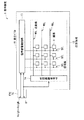
図1は、本技術の一実施の形態に係る表示装置1の概略構成を表したものである。この表示装置1は、例えば、表示パネル10と、表示パネル10に接続されたフレキシブルプリント基板(FPC:Flexible printed circuits)20(以下、FPC20と称する。)を備えている。
<1. Embodiment>
[Constitution]
FIG. 1 illustrates a schematic configuration of a
表示パネル10は、例えば、外部から入力された映像信号Vsig1〜VsigNおよび同期信号TPに基づいて映像を表示するものである。表示パネル10は、例えば、複数の画素11がマトリクス状に形成された画素領域12と、信号線駆動回路13と、走査線駆動回路14とを有している。表示パネル10は、例えば、各画素11が信号線駆動回路13および走査線駆動回路14によってアクティブ駆動されることにより、映像信号Vsig1〜VsigNに基づく映像を表示するものである。
The
表示パネル10は、行方向に延在する複数の書込線WSLと、列方向に延在する複数の信号線DTLとを有している。信号線DTLと書込線WSLとの交差部分に対応して、画素11が設けられている。各信号線DTLは、信号線駆動回路13の出力端に接続されている。各書込線WSLは、走査線駆動回路14の出力端に接続されている。
The
信号線駆動回路13は、例えば、FPC20を介して外部から入力された1水平ライン分のアナログの映像信号Vsig1〜VsigNを、各画素11に信号電圧として供給するものである。具体的には、信号線駆動回路13は、例えば、1水平ライン分のアナログの映像信号Vsig1〜VsigNを、走査線駆動回路14により選択された1水平ラインを構成する各画素11に、信号線DTLを介してそれぞれ供給するものである。
The signal
走査線駆動回路14は、例えば、FPC20を介して外部から入力された同期信号TPに応じて、駆動対象の画素11を選択するようになっている。具体的には、走査線駆動回路14は、例えば、走査線WSLを介して、選択パルスを画素11の画素回路15(後述)に印加することにより、マトリクス状に配置されている複数の画素11のうちの1行を駆動対象として選択するようになっている。そして、これらの画素11では、信号線駆動回路13から供給される信号電圧に応じて、1水平ラインの表示がなされる。このようにして、走査線駆動回路14は、例えば、時分割的に1水平ラインずつ順次走査を行い、画素領域12全体にわたった表示を行うようになっている。
For example, the scanning
図2は、画素11内の回路構成の一例を表したものである。各画素11は、例えば、画素回路15と、有機EL素子16とを有している。有機EL素子16は、例えば、アノード電極、有機発光層およびカソード電極が順に積層された構成を有している。画素回路15は、例えば、駆動トランジスタTr1、書込トランジスタTr2および保持容量Csによって構成されたものであり、2Tr1Cの回路構成となっている。書込トランジスタTr2は、駆動トランジスタTr1のゲートに対する信号電圧の印加を制御するものである。具体的には、書込トランジスタTr2は、信号線DTLの電圧をサンプリングするとともに駆動トランジスタTr1のゲートに書き込むものである。駆動トランジスタTr1は、有機EL素子16を駆動するものであり、有機EL素子16に直列に接続されている。駆動トランジスタTr1は、書込トランジスタTr2によって書き込まれた電圧の大きさに応じて有機EL素子16に流れる電流を制御するものである。保持容量Csは、駆動トランジスタTr1のゲート−ソース間に所定の電圧を保持するものである。なお、画素回路15は、上述の2Tr1Cの回路に対して各種容量やトランジスタを付加した回路構成となっていてもよいし、上述の2Tr1Cの回路構成とは異なる回路構成となっていてもよい。
FIG. 2 illustrates an example of a circuit configuration in the
駆動トランジスタTr1および書込トランジスタTr2は、例えば、nチャネルMOS型の薄膜トランジスタ(TFT(Thin Film Transistor))により形成されている。なお、TFTの種類は特に限定されるものではなく、例えば、逆スタガー構造(いわゆるボトムゲート型)であってもよいし、スタガー構造(トップゲート型)であってもよい。また、駆動トランジスタTr1および書込トランジスタTr2は、pチャネルMOS型のTFTにより形成されていてもよい。 The drive transistor Tr1 and the write transistor Tr2 are formed of, for example, an n-channel MOS thin film transistor (TFT (Thin Film Transistor)). Note that the type of TFT is not particularly limited, and may be, for example, an inverted staggered structure (so-called bottom gate type) or a staggered structure (top gate type). Further, the drive transistor Tr1 and the write transistor Tr2 may be formed of p-channel MOS type TFTs.
書込トランジスタTr2のゲートは、走査線WSLに接続されている。書込トランジスタTr2のソースおよびドレインの一方が信号線DTLに接続され、他方が駆動トランジスタTr1のゲートに接続されている。駆動トランジスタTr1のソースおよびドレインの一方が電源線Vccに接続され、他方が有機EL素子16のアノードに接続されている。保持容量Csの一端が駆動トランジスタTr1のゲートに接続され、保持容量Csの他端が駆動トランジスタTr1のソースおよびドレインのうち有機EL素子16側の端子に接続されている。
The gate of the writing transistor Tr2 is connected to the scanning line WSL. One of the source and drain of the write transistor Tr2 is connected to the signal line DTL, and the other is connected to the gate of the drive transistor Tr1. One of the source and drain of the drive transistor Tr1 is connected to the power supply line Vcc, and the other is connected to the anode of the
表示パネル10は、さらに、例えば、図2に示したように、有機EL素子16のカソードに接続されたグラウンド線GNDを有している。グラウンド線GNDは、グラウンド電位となっている外部回路と電気的に接続されるものである。グラウンド線GNDは、例えば、画素領域12全体に渡って形成されたシート状の電極である。グラウンド線GNDは、画素行または画素列に対応して短冊状に形成された帯状の電極であってもよい。
The
各画素11は、表示パネル10上の画面を構成する最小単位の点に対応するものである。表示パネル10は、カラー表示パネルとなっており、画素11は、例えば、赤、緑、または青などの単色の光を発するサブピクセルに相当する。画素11は、例えば、赤、緑、青、または白などの単色の光を発するサブピクセルに相当していてもよいし、赤、緑、青、または黄色などの単色の光を発するサブピクセルに相当していてもよい。以下では、画素11が、赤、緑、または青の単色の光を発するサブピクセルに相当するものとして、画素11の説明を行う。
Each
図3は、行方向に並んだ3つの画素11の行方向の断面構成の一例を表したものである。本実施の形態では、発光色の互いに異なる3つの画素11によって、カラー表示としての画素(カラー画素)が構成されている。カラー画素に含まれる3つの画素11は、赤色光を発する画素11R、緑色光を発する画素11G、および青色光を発する画素11Bで構成されている。各カラー画素において、3つの画素11は、行方向に一列に並んでおり、例えば、画素11R、画素11G、画素11Bの順で、正面左方向から右方向に向かって並んでいる。また、各カラー画素は、マトリクス状に配置されており、列方向に互いに隣接する2つの画素11が、互いに同一色の光を発するようになっている。つまり、画素領域12内の画素配列が、いわゆるストライプ配列となっている。
FIG. 3 illustrates an example of a cross-sectional configuration in the row direction of the three
表示パネル10は、例えば、画素回路15の形成された回路基板21上に複数の有機EL素子16を有している。有機EL素子16は、有機発光層24を画素電極22および透明電極25で挟み込んだ構造となっている。つまり、画素電極22および透明電極25は、画素領域12内に設けられている。画素電極22は、本技術の「第1電極」の一具体例に相当する。透明電極25は、本技術の「第2電極」の一具体例に相当する。画素電極22は、有機発光層24との関係で、回路基板21側に形成されており、例えば、有機EL素子16のアノード電極として機能する。画素電極22は、画素11ごとに独立に設けられたものである。複数の画素電極22は、表示パネル10内の一の面内においてマトリクス状に配置されている。画素電極22は、金属材料で構成されており、有機発光層24から発せられた光を透明電極25側に反射する反射ミラーとしても機能する。
The
一方、透明電極25は、有機発光層24との関係で、回路基板21とは反対側に形成されており、例えば、有機EL素子16のカソード電極として機能する。透明電極25は、画素領域12全体に渡って形成されたシート状の電極である。透明電極25は、画素行または画素列に対応して短冊状に形成された帯状の電極であってもよい。透明電極25は、例えば、上述のグラウンド線GNDに相当している。透明電極25は、各画素11において共通の電極として機能する。
On the other hand, the
透明電極25は、可視光を透過可能な電極であり、光透過性の導電性材料によって構成されている。光透過性の導電性材料は、例えば、Mg、Ag、Al、CuおよびAuのうち少なくとも1つを含む金属もしくは合金で構成されている。光透過性の導電性材料は、上記金属もしくは上記合金に、CaおよびLiのうち少なくとも1つが含まれた材料で構成されていてもよい。上記金属もしくは上記合金に、CaおよびLiのうち少なくとも1つが含まれることにより、導電性材料の光透過性(透明性)が向上する。光透過性の導電性材料は、例えば、CaおよびLiのうち少なくとも1つと、Mgと、Agとを含む金属もしくは合金で構成されている。透明電極25が、上述したような金属もしくは合金で構成されている場合、透明電極25は、気相成膜法(例えば、蒸着法)によって形成されている。光透過性の導電性材料は、例えば、ITOまたはIZOなどで構成されていてもよい。透明電極25が、ITOまたはIZOで構成されている場合、透明電極25は、気相成膜法(例えば、スパッタ法)によって形成されている。
The
有機発光層24は、例えば、画素電極22側から順に、正孔注入効率を高める正孔注入層と、発光層への正孔輸送効率を高める正孔輸送層と、電子と正孔との再結合による発光を生じさせる発光層と、発光層への電子輸送効率を高める電子輸送層とを有している。有機発光層24は、白色光を発する構成となっている。上記の発光層は、例えば、画素電極22側から順に、赤色光を発する発光層、緑色光を発する発光層、および青色光を発する発光層を含む積層構造となっている。正孔注入層、正孔輸送層、発光層および電子輸送層は、例えば、特開2012−209095に記載の材料により構成されている。有機発光層24は、気相成膜法(例えば、蒸着法)によって形成されている。
The organic
表示パネル10は、例えば、図3に示したように、互いに隣接する有機EL素子16の間隙に絶縁層23を有している。絶縁層23は、互いに隣接する画素電極22を互いに絶縁分離するとともに、発光領域を正確に所望の形状にする画素定義膜である。絶縁層23は、画素電極22と同一の面上に形成されており、画素電極22の周囲を埋め込んでいる。絶縁層23の上面は、画素電極22の上面よりも高い位置にある。絶縁層23は、画素電極22の上面と対向する位置に、発光領域の形状を規定する開口(画素開口部23A)を有している。画素開口部23Aは、本技術の「第1開口」の一具体例に相当する。有機発光層24は、少なくとも画素開口部23Aの内部に形成されており、画素電極22の上面のうち、画素開口部23Aの底面に露出している部分に接している。透明電極25も、少なくとも画素開口部23Aの内部に形成されており、有機発光層24の上面のうち、少なくとも画素開口部23Aの直上部分に接している。絶縁層23は、可視光を透過可能な樹脂材料で構成されており、例えば、ポリイミドによって構成されている。
For example, as shown in FIG. 3, the
表示パネル10は、例えば、回路基板21と所定の間隙を介して対向する位置に対向基板29を有している。対向基板29は、画素回路15や有機EL素子16等を保護するものであり、例えば、ガラス基板または光透過性の樹脂基板で構成されている。表示パネル10は、例えば、対向基板29の裏面(回路基板21側の面)に、カラーフィルタ27およびブラックマトリクス28を有している。
The
カラーフィルタ27は、画素電極22と対向する位置に配置されており、少なくとも画素11内に配置されている。カラーフィルタ27は、有機発光層24から発せられた光を所望の波長帯において選択的に透過するものである。カラーフィルタ27は、例えば、画素11R、画素11G、画素11Bごとに、選択的に透過させる光の波長帯を異ならせている。カラーフィルタ27は、例えば、赤色光を選択的に透過する赤色フィルタ27Rを画素11Rに有し、緑色光を選択的に透過する緑色フィルタ27Gを画素11Gに有し、青色光を選択的に透過する青色フィルタ27Bを画素11Bに有している。
The
ブラックマトリクス28は、画素電極22と非対向の位置(つまり画素11周囲)に配置されており、例えば、カラーフィルタ27と同一面内に配置されている。ブラックマトリクス28は、画素領域12において画素11の周囲から漏れる光を遮断するものであり、例えば、有機発光層24から発せられた光を吸収する材料を含んで構成されている。
The
表示パネル10は、例えば、回路基板21と対向基板29との間隙に、絶縁層26を有している。絶縁層26は、回路基板21と対向基板29との間隙を埋め込むように形成されている。絶縁層26は、例えば、透明電極25と、カラーフィルタ27およびブラックマトリクス28との間に配置されており、透明電極25と、カラーフィルタ27およびブラックマトリクス28とに接している。絶縁層26は、可視光を透過可能な樹脂材料で構成されており、例えば、ポリイミドによって構成されている。
The
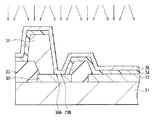
図4は、1つの画素11およびその近傍の列方向の断面構成の一例を表したものである。図5は、図4における補助配線30(後述)近傍の断面構成を拡大して表したものである。図6は、画素領域12における画素電極22(22R、22G、22B)、補助配線30、隔壁31(後述)およびコンタクト領域30A(後述)のレイアウトの一例を表したものである。なお、図3の断面は、図6のA−A矢視方向の断面に対応している。図4、図5の断面は、図6のB−B矢視方向の断面に対応している。図7は、画素領域12における有機発光層24、隔壁31およびコンタクト領域30Aのレイアウトの一例を表したものである。
FIG. 4 illustrates an example of a cross-sectional configuration in the column direction of one
表示パネル10は、例えば、画素11(もしくは画素電極22)の周囲に複数の補助配線30を有している。補助配線30は、画素電極22に隣接して設けられており、複数の画素電極22のうち互いに隣接する2つの画素電極22の間隙に設けられている。補助配線30が、本技術の「金属部材」の一具体例に相当する。補助配線30は、透明電極25の電気抵抗が大きいことに起因する電圧降下を低減するためのものである。補助配線30は、回路基板21上に形成されており、例えば、画素電極22と同一面内に配置されている。補助配線30は、例えば、製造過程において、画素電極22と一括して形成されたものであり、画素電極22と同一材料、同一厚さとなっている。補助配線30は、例えば、Au、Pt、Ni、Cr、Cu、W、MoおよびAgのうち少なくとも1種類の材料を含む金属もしくは合金で構成されている。複数の補助配線30は、画素電極22と絶縁分離された状態で、画素11の周囲に張り巡らされている。複数の補助配線30は、例えば、列方向に互いに隣接する2つの画素11の間隙において、行方向に延在している。
The
補助配線30は、画素電極22とは異なる面内に形成されていてもよく、例えば、画素電極22よりも下層に形成されていてもよい。ただし、この場合には、表示パネル10は、例えば、画素11(もしくは画素電極22)の周囲に、補助配線30と電気的に接続されたパッド状の複数の補助電極を有していることが好ましい。補助電極は、画素電極22に隣接して設けられており、複数の画素電極22のうち互いに隣接する2つの画素電極22の間隙に設けられている。補助電極が、本技術の「金属部材」の一具体例に相当する。補助電極は、透明電極25の電気抵抗が大きいことに起因する電圧降下を低減するためのものである。補助電極は、回路基板21上に形成されており、例えば、画素電極22と同一面内に配置されている。補助電極は、例えば、製造過程において、画素電極22と一括して形成されたものであってもよく、画素電極22と同一材料、同一厚さとなっていてもよい。補助電極は、例えば、Au、Pt、Ni、Cr、Cu、W、MoおよびAgのうち少なくとも1種類の材料を含む金属もしくは合金で構成されている。複数の補助電極は、画素電極22と絶縁分離された状態で、画素11の周囲に配置されている。複数の補助電極は、例えば、列方向に互いに隣接する2つの画素11の間隙に配置されている。
The
絶縁層23は、互いに隣接する画素電極22および補助配線30を絶縁分離しており、補助配線30の周囲を埋め込んでいる。絶縁層23の上面は、補助配線30の上面よりも高い位置にある。絶縁層23は、補助配線30の上面と対向する位置に、補助配線30と透明電極25とを互いに電気的に接続するための開口(コンタクト開口部23B)を有している。コンタクト開口部23Bは、本技術の「第2開口」の一具体例に相当する。透明電極25は、コンタクト開口部23Bの内部にも形成されており、補助配線30の上面のうち、コンタクト開口部23Bの底面に露出している部分の一部に接している。以下では、コンタクト開口部23Bの底面のうち、透明電極25が接している部分をコンタクト領域30Aと称するものとする。コンタクト領域30Aは、補助配線30の上面のうち、絶縁層23および後述の隔壁31で覆われていない領域である。なお、上述した補助電極が設けられている場合には、本段落以降における「補助配線30」を「補助電極」に読み替えるものとする。
The insulating
表示パネル10は、各コンタクト領域30Aに隣接する位置に隔壁31を有している。隔壁31と画素電極22との間には、コンタクト領域30Aが存在している。つまり、隔壁31は、面内において、コンタクト領域30Aを介して、画素電極22と対向して配置されている。コンタクト領域30Aおよび隔壁31は、例えば、列方向に互いに隣接する2つの画素11(または2つの画素電極22)の間隙に配置されている。なお、本実施の形態では、コンタクト領域30Aおよび隔壁31は、例えば、行方向に互いに隣接する2つのカラー画素の間隙に配置されていてもよい。隔壁31は、製造過程において、有機発光層24を面内において選択的に形成するために使われるものである。隔壁31は、当該隔壁31の上面にも形成される透明電極25を介して対向基板29もしくはブラックマトリクス28に接していてもよい。この場合、隔壁31は、例えば、対向基板29を支持する役割も持っている。なお、隔壁31の上面にも形成される透明電極25が対向基板29もしくはブラックマトリクス28に接しない程度に、隔壁31が低く形成されていてもよい。
The
隔壁31は、補助配線30の上面のうち、コンタクト開口部23Bの底面に露出している部分の一部に接している。具体的には、隔壁31は、コンタクト開口部23Bの底面のうち、コンタクト領域30A以外の領域に接している。有機発光層24が、例えば、上述したように、気相成膜法(例えば、蒸着法)を用いて形成される場合、有機発光層24は、隔壁31の背後に位置する領域(コンタクト領域30A)を除いて、画素領域12全面に形成される。製造過程における隔壁31の使い方にも依るが、コンタクト開口部23Bの底面の一部には、有機発光層24が形成される(接する)場合もあるし、コンタクト開口部23Bの底面には、有機発光層24が形成されない(接しない)場合もある。つまり、有機発光層24は、補助配線30の上面のうち、コンタクト開口部23Bの底面に露出している部分(第1領域)の全体または一部を除き、画素電極22の上面のうち、画素開口部23Aの底面に露出している領域(第2領域)を含む表面に設けられている。従って、隔壁31は、コンタクト開口部23Bの底面のうち、有機発光層24に非接触の領域である非接触領域30aの一部に接している。厳密に言うと、隔壁31は、コンタクト開口部23Bの底面のうち、コンタクト領域30Aと、有機発光層24が接している領域とを除いた領域に接している。
The
隔壁31は、さらに、絶縁層23にも接している。具体的には、隔壁31は、コンタクト開口部23Bの側面のうち、非接触領域30aに隣接する領域(隣接側面30b)と、絶縁層23の上面のうち、隣接側面30bに隣接する領域(隣接上面30c)とに接している。つまり、隔壁31は、非接触領域30aの一部、隣接側面30b、および隣接上面30cの3箇所全てに接している。隔壁31は、絶縁層23とは別工程で形成されたものであり、隔壁31と絶縁層23との間には、界面が存在している。
The
隔壁31は、例えば、金属材料、無機材料、または有機材料によって構成されている。隔壁31に使用可能な金属材料としては、例えば、Al、Ag、Mo、Ti、W、Cu、またはそれらのうち少なくとも1つを含む合金が挙げられる。また、隔壁31に使用可能な金属材料としては、例えば、ITOまたはIZOが挙げられる。隔壁31が上述したような金属材料によって構成されている場合、隔壁31は、例えば、スパッタ法により金属材料を成膜した後、フォトリソグラフィ法およびウエットエッチング法により所定の形状に成形することにより形成されている。隔壁31は、例えば、以下のようにして形成される。まず、スパッタ法によりAlおよびMoをこの順に積層成膜した後、その上に、フォトリソグラフィ法で所定の形状に成形された所望のパターンのレジストを形成する。次に、そのレジストをマスクとして、AlおよびMoの積層膜をリン酸と硝酸と酢酸の混酸に浸漬させてエッチングしたりした後、レジストを、O2プラズマに曝したり、有機溶剤等の剥離液で溶解させたりすることにより除去する。このようにして、隔壁31を形成することができる。隔壁31に使用可能な無機材料としては、例えば、SiO2、SiNまたはSiONが挙げられる。隔壁31が上述したような無機材料によって構成されている場合、隔壁31は、例えば、CVD法により無機材料を成膜したのち、フォトリソグラフィ法およびウエットエッチング法により所定の形状に成形することにより形成されている。隔壁31は、例えば、以下のようにして形成される。まず、CVD法によりSiO2を成膜した後、その上に、フォトリソグラフィ法で所定の形状に成形された所望のパターンのレジストを形成する。次に、そのレジストをマスクとして、SiO2膜をフッ化水素酸に浸漬させてエッチングした後、レジストを、O2プラズマに曝したり、有機溶剤等の剥離液で溶解させたりすることにより除去する。このようにして、隔壁31を形成することができる。隔壁31に使用可能な有機材料としては、例えば、感光性樹脂が挙げられる。感光性樹脂としては、例えば、ポリイミド樹脂、ポリアミド樹脂、アクリル樹脂、ノボラック樹脂、ポリヒドロキシスチレン樹脂などが挙げられる。隔壁31が上述したような有機材料によって構成されている場合、隔壁31は、例えば、感光性樹脂を塗布し、フォトリソグラフィ法で所定の形状に成形した後、成形した感光性樹脂を加熱硬化させることにより形成されている。
The
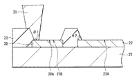
隔壁31や絶縁層23の断面形状(列方向の断面形状)は、例えば、以下の式(1)〜(3)を満たしている。
θ1 ≦ 90°…(1)
tanθ3 = h/x…(2)
θ2 < θ3 < θ1…(3)
θ1:隔壁31の側面と底面(補助電極30の上面)とのなす角度
(隔壁31の側面の傾斜角)
θ2:画素開口部23Aの側面(内面)と画素電極22とのなす角度
(画素開口部23Aの側面(内面)の傾斜角)
θ3:隔壁31の上面の端縁と、コンタクト開口部23Bの底面に接する有機発光層24の端縁とを結んだ線分と、コンタクト開口部23Bの底面(補助電極30の上面)とのなす角度
h:隔壁31の、底面(補助電極30の上面)からの高さ
x:隔壁31の上面の端縁から、コンタクト開口部23Bの底面(補助電極30の上面)に垂直に下ろした線分と、コンタクト開口部23Bの底面(補助電極30の上面)とが互いに交差する点と、コンタクト開口部23Bの底面に接する有機発光層24の端縁との距離
The cross-sectional shape (cross-sectional shape in the column direction) of the
θ1 ≦ 90 ° (1)
tan θ3 = h / x (2)
θ2 <θ3 <θ1 (3)
θ1: Angle formed between the side surface of the
θ2: angle formed by the side surface (inner surface) of the
θ3: A line segment connecting the edge of the upper surface of the
隔壁31や絶縁層23の断面形状が上記の式(1)〜(3)を満たす場合、画素開口部23Aの側面(内面)がテーパー状となっており、隔壁31の側面がテーパー状または垂直となっていることになる。さらに、画素開口部23Aの側面(内面)が、隔壁31の側面よりも斜めに傾斜していることになる。そのため、例えば、角度θ3で斜め蒸着を行うことにより、隔壁31の背後にコンタクト領域30Aを形成しつつ、有機発光層24を画素開口部23Aの底面全体に形成することができる。
When the cross-sectional shapes of the
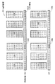
次に、隔壁31の平面形状について説明する。図8A〜図8Fは、隔壁31の平面形状の一例を表したものである。隔壁31は、コンタクト領域30Aの辺部に接して形成されている。コンタクト領域30Aが方形状となっている場合、隔壁31は、コンタクト領域30Aの少なくとも1辺に接して形成されている。コンタクト領域30Aが方形状となっている場合、隔壁31は、例えば、コンタクト領域30Aの1辺だけに接して形成されている。このとき、隔壁31の平面形状は、例えば、図8Fに示したような方形状となっている。また、コンタクト領域30Aが方形状となっている場合、隔壁31は、例えば、コンタクト領域30Aの2辺だけに接して形成されており、このとき、隔壁31の平面形状は、例えば、図8Dに示したようなL字形状となっている。また、コンタクト領域30Aが方形状となっている場合、隔壁31は、例えば、コンタクト領域30Aの3辺だけに接して形成されており、このとき、隔壁31の平面形状は、例えば、図8A、図8Cに示したようなH字形状またはU字形状(もしくはカタカナのコ字形状)となっている。
Next, the planar shape of the
コンタクト領域30Aが円形状、半円形状、楕円形状、または半楕円形状となっている場合、隔壁31は、コンタクト領域30Aの曲線状の辺に接して形成されている。このとき、隔壁31の平面形状は、例えば、図8Bに示したようなC字形状となっている。コンタクト領域30Aが三角形状となっている場合、隔壁31は、コンタクト領域30Aの2辺に接して形成されている。このとき、隔壁31の平面形状は、例えば、図8Eに示したようなV字形状となっている。
When the
隔壁31は、面内において、コンタクト領域30Aの一部を180°以上、360°未満の範囲で囲むように形成されていることが好ましい。図8A、図8B、図8C、図8Eに記載の隔壁31は、この条件に合致している。さらに、隔壁31は、例えば、図8A、図8B、図8Cまたは図8Eに示したように、面内方向に、180°以外の2方向に突出する凸部31Aを有していることが好ましい。隔壁31がそのような凸部31Aを有している場合、隔壁31が、透明電極25を介して、対向基板29またはブラックマトリクス28に接しているときであっても、隔壁31が剥離し難い。なお、上述の「コンタクト領域30Aの一部」は、特に限定されるものではないが、例えば、コンタクト領域30Aの平面形状における重心位置であってもよい。
The
[製造方法]
次に、本実施の形態の表示装置1の製造方法の一例について説明する。図9〜図11は、表示装置1の製造工程の一例を工程順に表した断面図である。まず、回路基板21上に、気相成膜法(例えば、スパッタ法)により金属材料膜を形成した後、例えば、フォトリソグラフィおよびエッチングにより所定の形状に成形する。これにより、回路基板21上に、画素電極22および補助電極30を形成する(図9参照)。なお、上記と同様の方法を用いて、画素電極22と、補助電極30とを互いに別の工程で形成するようにしてもよい。
[Production method]
Next, an example of a method for manufacturing the
次に、画素電極22および補助電極30を含む表面全体に、例えば、ポリイミドなどの感光性絶縁樹脂を塗布した後、フォトリソグラフィによる露光および現像を行う。これにより、画素電極22上に画素開口部23Aを形成し、補助電極30上にコンタクト開口部23Bを形成する(図9参照)。次に、画素開口部23Aおよびコンタクト開口部23Bを有する絶縁層23の表面全体に、例えば、ポリイミドなどの感光性絶縁樹脂を塗布した後、フォトリソグラフィによる露光および現像を行う。これにより、コンタクト開口部23Bの底面の一部から、コンタクト開口部23Bの側面、絶縁層23の上面に渡って隔壁31を形成する(図9)。このときに、隔壁31や絶縁層23の断面形状が、上記の式(1)〜(3)を満たすように、感光性絶縁樹脂の厚さや露光強度などを調整することが好ましい。
Next, for example, a photosensitive insulating resin such as polyimide is applied to the entire surface including the
次に、例えば、気相成膜法(例えば、斜め蒸着法)により、表面全体に有機発光層24を形成する(図10)。このとき、コンタクト領域30Aを形成することとなる領域が隔壁31の背後(影)となるよう、有機発光層24の材料の、補助電極30の上面に対する入射方向を設定する。さらに、有機発光層24の材料の、補助電極30(または画素電極22)の上面に対する入射角を角度θ3に設定することが好ましい。このようにした結果、コンタクト開口部23Bの底面に、補助電極30の上面の一部を露出させたまま(つまり、コンタクト領域30Aを形成しつつ)、画素開口部23Aの底面に露出する画素電極22の上面全体に有機発光層24を形成することができる。
Next, the organic
次に、例えば、有機発光層24形成時の気相成膜法と比べて入射角の偏りを減じた気相成膜法により、表面全体に透明電極25を形成する(図11)。これにより、コンタクト領域30Aにおいて、補助配線30と透明電極25とを互いに電気的に接続することができる。なお、蒸着法において、有機発光層24形成時の気相成膜法と比べて入射角の偏りを減じる方法としては、例えば、回路基板21を回転台に載せ、回路基板21を回転させることが考えられる。また、蒸着法の代わりに、スパッタ法を用いることも考えられる。これにより、様々な方向から有機発光層24の材料を回路基板21に入射させることができる。その後、例えば、透明電極25上に、ポリイミドなどの感光性絶縁樹脂を塗布した後、対向基板29を、カラーフィルタ27およびブラックマトリクス28を介して感光性絶縁樹脂に張り合わせ、感光性絶縁樹脂を硬化させる。このようにして、表示装置1が製造される。
Next, the
[効果]
次に、本実施の形態の表示装置1における効果について説明する。
[effect]
Next, the effect in the
図12は、比較例に係る表示パネルの画素領域120における画素電極122R、122G、122B、補助配線130およびコンタクト領域130Aのレイアウトの一例を表したものである。なお、画素電極122R、122G、122Bは、本実施の形態の画素電極22R、22G、22Bに対応するものである。補助配線130は、本実施の形態の補助配線30に対応するものである。コンタクト領域130Aは、補助配線130の上面の一部であり、例えば、コンタクト領域130Aのうち絶縁層で覆われずに露出している領域である。
FIG. 12 illustrates an example of the layout of the
本比較例において、例えば、本実施の形態の透明電極25に対応する透明電極と、補助配線130とを互いに電気的に接続させる方法として、例えば、特許文献1に記載された方法と同様にして、コンタクト領域130Aに透明電極を成膜することが考えられる。この場合、透明電極を成膜する前段の有機発光層240の成膜において、有機発光層240がコンタクト領域130Aに形成されることのないよう、有機発光層の形成領域をコンタクト領域から遠ざけることが必要となる(図13)。これは、コンタクト領域130Aと透明電極との電気的な接続を担保するためである。しかし、そのようにした場合には、有機発光層240の形成領域が小さくなり、開口率が小さくなってしまう。
In this comparative example, for example, as a method of electrically connecting the transparent electrode corresponding to the
そこで、例えば、特許文献2,3に記載された方法と同様にして、有機発光層を全面に形成したのち、その一部を除去することによりコンタクト領域を形成することが考えられる。しかし、そのようにした場合には、有機発光層の除去工程における残留物に起因して歩留まりが低下する可能性がある。
Therefore, for example, it is conceivable to form a contact region by forming an organic light emitting layer on the entire surface in the same manner as described in
一方、本実施の形態では、隔壁31が、補助配線30上のコンタクト開口部23Bの底面の一部および絶縁層23に接して配置されている。これにより、例えば、気相成膜法(例えば、蒸着法)を用いて、有機発光層24を形成することにより、隔壁31の背後(または影)に、コンタクト領域30Aを形成しつつ、画素開口部23Aの底面を含む表面に有機発光層24を形成することができる。つまり、有機発光層24がコンタクト領域30Aに形成されないようする際にマスクは不要である。また、コンタクト領域30Aの形成にはマスクが不要であることから、コンタクト領域30Aの周囲には、マスクの精度や、マスクの位置ずれなどを考慮したマージンが不要である。そのため、そのマージンが不要な分だけ、画素電極22や有機発光層24を広く形成することができる。従って、有機発光層24の除去工程を利用しないでコンタクト領域30Aを形成することができ、かつ開口率を大きくすることができる。
On the other hand, in the present embodiment, the
また、本実施の形態では、隔壁31が、補助配線30上のコンタクト開口部23Bの底面の一部および絶縁層23に接して配置されている。これにより、隔壁31が補助配線30上だけに接して配置されている場合と比べて、隔壁31の剥離を生じ難くさせることができる。例えば、絶縁層23および隔壁31がともに有機材料(疎水性)によって構成されている場合、絶縁層23と隔壁31との密着性が高く、隔壁31の剥離を生じ難くさせることができる。また、例えば、絶縁層23および隔壁31がともに無機材料(親水性)によって構成されている場合、絶縁層23と隔壁31との密着性ならびに画素電極22と隔壁31との密着性が高く、隔壁31の剥離を生じ難くさせることができる。また、例えば、絶縁層23と隔壁31との材料の種類(疎水性または親水性)が異なる場合であって、かつ隔壁31が金属材料(親水性)または無機材料(親水性)によって構成されているときには、画素電極22と隔壁31との密着性は高く、絶縁層23と隔壁31との密着性は比較的高い。従って、この場合にも、隔壁31の剥離を生じ難くさせることができる。なお、金属材料(親水性)または無機材料(親水性)上に有機材料(疎水性)を塗布した場合、有機材料に含まれる界面活性剤による作用によって金属材料または無機材料と有機材料との密着性が阻害される可能性がある。そのため、絶縁層23が無機材料(親水性)によって構成され、隔壁31が有機材料(疎水性)によって構成さている場合の、絶縁層23と隔壁31との密着性や、画素電極22と隔壁31との密着性は、あまり高くはならない。しかし、この場合には、例えば、隔壁31を、図8A、図8B、図8C、図8Eに記載したような、剥離し難い平面形状とし、絶縁層23と隔壁31との密着性の不十分さを補うことにより、隔壁31の剥離を抑えることができる。また、本実施の形態では、画素開口部23Aの側面が、隔壁31の側面よりも斜めに傾斜している。これにより、例えば、気相成膜法(例えば、蒸着法)を用いて、有機発光層24を形成したときに、画素開口部23Aの底面全体に、有機発光層24を形成させる(接触させる)ことができる。
In the present embodiment, the
また、本実施の形態において、隔壁31が、面内において、コンタクト領域30Aの一部を180°以上、360°未満の範囲で囲むように形成されている場合には、隔壁31の剥離を生じ難くさせることができる。さらに、隔壁31を小型化しても、有機光学層24の材料の、コンタクト領域30Aへの付着を効果的に遮蔽することができる。その結果、隔壁31を小型化できた分だけ、開口率を大きくすることができる。また、隔壁31が、面内方向に、180°以外の2方向に突出する凸部31Aを有している場合にも、隔壁31の剥離を生じ難くさせることができる。このように、隔壁31が隔壁31の剥離を生じ難くする構成となっている場合、例えば、気相成膜法により透明電極25を形成する際に、透明電極25の材料がコンタクト領域30Aに回り込む量が少なくなり、コンタクト領域30Aでの抵抗値が増大しやすい。そのため、透明電極25を厚く形成することが考えられる。本実施の形態において、透明電極25が、CaおよびLiの少なくとも一方を含む光透過性の導電性材料で構成されている場合、透明電極25を厚く形成したとしても、透明電極25の光透過性(透明性)の低下を抑制することができる。その結果、表示装置1の光学特性の低下を抑制しつつ、コンタクト領域30Aでの抵抗値の増大も抑制し、表示装置1の画品位を改善することができる。
Further, in the present embodiment, when the
<2.変形例>
以下に、上記実施の形態の表示装置1の種々の変形例について説明する。なお、以下では、上記実施の形態の表示装置1と共通する構成要素に対しては、同一の符号が付与される。さらに、上記実施の形態の表示装置1と共通する構成要素についての説明は、適宜、省略されるものとする。
<2. Modification>
Below, the various modifications of the
[変形例1]
上記実施の形態では、隔壁31の側面がテーパー状となっている場合が例示されていたが、例えば、図14に示したように、逆テーパー状となっていてもよい。このとき、隔壁31や絶縁層23の断面形状は、例えば、上記の式(2)と、以下の式(4)、(5)を満たしている。
90° < θ1 ≦ 180°…(4)
θ2 < θ3 ≦ 90°…(5)
[Modification 1]
In the embodiment described above, the case where the side surface of the
90 ° <θ1 ≦ 180 ° (4)
θ2 <θ3 ≦ 90 ° (5)
隔壁31や絶縁層23の断面形状が上記の式(2)、(4)、(5)を満たす場合、隔壁31の側面の直下に空隙が存在し、その空隙の底面がコンタクト領域30Aとなる。さらに、画素開口部23Aの側面(内面)が、隔壁31の上面の端縁と、コンタクト開口部23Bの底面に接する有機発光層24の端縁とを結んだ線分よりも斜めに傾斜していることになる。そのため、例えば、角度θ3で斜め蒸着を行ったり、画素電極22の上面に対して垂直な方向から蒸着を行ったりすることにより、隔壁31の背後にコンタクト領域30Aを形成しつつ、有機発光層24を画素開口部23Aの底面全体に形成することができる。
When the cross-sectional shapes of the
次に、本変形例に係る表示装置1の製造方法の一例について説明する。図15〜図17は、表示装置1の製造工程の一例を工程順に表した断面図である。なお、絶縁層23を作るまでの工程は、上記実施の形態と同様であるので、以下では、それ以降の工程について説明する。
Next, an example of a method for manufacturing the
絶縁層23を形成した後、画素開口部23Aおよびコンタクト開口部23Bを有する絶縁層23の表面全体に、例えば、ポリイミドなどの感光性絶縁樹脂を塗布する。続いて、フォトリソグラフィによる露光および現像を行う。これにより、コンタクト開口部23Bの底面の一部から、コンタクト開口部23Bの側面、絶縁層23の上面に渡って隔壁31を形成する(図15)。このときに、隔壁31や絶縁層23の断面形状が、上記の式(2)、(4)、(5)を満たすように、感光性絶縁樹脂の厚さや露光強度などを調整することが好ましい。
After the insulating
次に、例えば、気相成膜法(例えば、斜め蒸着法)により、表面全体に有機発光層24を形成する(図16)。このとき、コンタクト領域30Aを形成することとなる領域が隔壁31の背後(影)となるよう、有機発光層24の材料の、補助電極30の上面に対する入射方向を設定する。さらに、有機発光層24の材料の、補助電極30(または画素電極22)の上面に対する入射角を角度θ3に設定することが好ましい。このようにした結果、コンタクト開口部23Bの底面に、補助電極30の上面の一部を露出させたまま(つまり、コンタクト領域30Aを形成しつつ)、画素開口部23Aの底面に露出する画素電極22の上面全体に有機発光層24を形成することができる。
Next, the organic
次に、例えば、有機発光層24形成時の気相成膜法と比べて入射角の偏りを減じた気相成膜法により、表面全体に透明電極25を形成する(図17)。これにより、コンタクト領域30Aにおいて、補助配線30と透明電極25とを互いに電気的に接続することができる。なお、蒸着法において、有機発光層24形成時と比べて入射角の偏りを減じる方法としては、例えば、回路基板21を回転台に載せ、回路基板21を回転させることが考えられる。また、蒸着法の代わりに、スパッタ法を用いることも考えられる。これにより、様々な方向から有機発光層24の材料を回路基板21に入射させることができる。その後、例えば、透明電極25上に、ポリイミドなどの感光性絶縁樹脂を塗布した後、対向基板29を、カラーフィルタ27およびブラックマトリクス28を介して感光性絶縁樹脂に張り合わせ、感光性絶縁樹脂を硬化させる。このようにして、本変形例に係る表示装置1が製造される。
Next, the
本変形例に係る表示装置1は、例えば、以下に示した方法で製造することも可能である。図18、図19は、本変形例に係る表示装置1の製造工程の他の例を工程順に表した断面図である。なお、隔壁31を作るまでの工程は、上記の製造方法と同様であるので、以下では、それ以降の工程について説明する。
The
隔壁31を形成した後、例えば、気相成膜法(例えば、蒸着法)により、表面全体に有機発光層24を形成する(図18)。例えば、有機発光層24の材料の主な入射角を、補助電極30(または画素電極22)に垂直にする。つまり、気相成膜法として、垂直蒸着法を用いる。このとき、隔壁31の逆テーパー状の側面の直下には、有機発光層24の材料が入り込みにくい。そのため、コンタクト開口部23Bのうち、隔壁31の逆テーパー状の側面の直下に対応する部分がコンタクト領域30Aとなる。従って、コンタクト開口部23Bの底面に、補助電極30の上面の一部を露出させたまま(つまり、コンタクト領域30Aを形成しつつ)、画素開口部23Aの底面に露出する画素電極22の上面全体に有機発光層24を形成することができる。
After the
次に、例えば、有機発光層24形成時の気相成膜法と比べて入射角の偏りを減じた気相成膜法により、表面全体に透明電極25を形成する(図19)。これにより、コンタクト領域30Aにおいて、補助配線30と透明電極25とを互いに電気的に接続することができる。なお、蒸着法において、有機発光層24形成時と比べて入射角の偏りを減じる方法としては、例えば、回路基板21を回転台に載せ、回路基板21を回転させることが考えられる。また、蒸着法の代わりに、スパッタ法を用いることも考えられる。これにより、様々な方向から透明電極25の材料を回路基板21に入射させることができる。その後、例えば、透明電極25上に、ポリイミドなどの感光性絶縁樹脂を塗布した後、対向基板29を、カラーフィルタ27およびブラックマトリクス28を介して感光性絶縁樹脂に張り合わせ、感光性絶縁樹脂を硬化させる。このようにして、本変形例に係る表示装置1が製造される。
Next, the
[変形例2]
上記変形例1では、補助配線30の上面が平坦面となっていたが、例えば、図20に示したように、補助配線30の上面のうちコンタクト開口部23Bの底面に露出している部分(コンタクト領域30A)が傾斜面30Bとなっていてもよい。傾斜面30Bは、隔壁31の側面から遠ざかるにつれて下り坂となるように形成されている。傾斜面30Bと隔壁31の側面とのなす角度が、概ね90°となることが好ましく、90°よりも若干大きくなっていてもよい。傾斜面30Bは、滑らかな面となっていてもよいし、階段状の面となっていてもよい。回路基板21は、補助配線30に傾斜面30Bの形成されている部分の直下において、平坦面となっている。補助配線30では、傾斜面30Bの形成されている部分において、厚みが他の部分と比べて薄くなっている。補助配線30に傾斜面30Bを形成する方法としては、例えば、補助配線30の上面を部分的にエッチングすることが考えられる。
[Modification 2]
In the first modification, the upper surface of the
本変形例では、補助配線30の上面のうちコンタクト開口部23Bの底面に露出している部分が傾斜面30Bとなっている。これにより、例えば、有機発光層24形成時の気相成膜法と比べて入射角の偏りを減じた気相成膜法により、表面全体に透明電極25を形成したときに、コンタクト領域30Aに透明電極25を十分な厚さで形成することができる。その結果、コンタクト領域30Aにおける、補助配線30と透明電極25との電気的な接続をより確実にすることができる。
In the present modification, a portion of the upper surface of the
[変形例3]
上記変形例2では、補助配線30に傾斜面30Bを設けることで、補助配線30の上面のうちコンタクト開口部23Bの底面に露出している部分が傾斜面30Bとなっていた。しかし、例えば、図21に示したように、回路基板21の上面のうち、コンタクト開口部23Bの底面の直下に対応する部分に、すり鉢状の窪み21Aを設け、補助配線30の一部を、すり鉢状の窪み21Aの内部に配置してもよい。このようにした場合であっても、補助配線30の上面のうちコンタクト開口部23Bの底面に露出している部分を、傾斜面30Bとすることができる。
[Modification 3]
In the second modification, by providing the
つまり、本変形例では、回路基板21は、コンタクト開口部23Bの底面の直下に対応する部分に、すり鉢状の窪み21Aを有している。そして、補助配線30の一部が、すり鉢状の窪み21Aの内部に配置されている。このとき、補助配線30は、場所に寄らず概ね均一な厚さとなっている。従って、本変形例では、補助配線30の厚さを場所に寄らず概ね均一にしたままの状態で、補助配線30の上面のうちコンタクト開口部23Bの底面に露出している部分を傾斜面30Bにすることができる。
That is, in this modification, the
[製造方法]
次に、本変形例に係る表示装置1の製造方法の一例について説明する。図22A、図22Bは、本変形例に係る表示装置1の製造工程の一例を工程順に表した断面図である。なお、本変形例において、回路基板21は、画素回路15の形成された回路基板21aの上面に、平坦化膜21bを有している。平坦化膜21bは、例えば、フォトリソグラフィによる露光および現像を行うことの可能な材料で構成されており、例えば、感光性絶縁樹脂で構成されている。
[Production method]
Next, an example of a method for manufacturing the
まず、回路基板21上に、所定の位置に開口部100Aおよびグレイトーン開口部100Bを有するマスク100を配置する(図22A)。開口部100Aは、マスク100を貫通する貫通孔である。グレイトーン開口部100Bは、貫通孔よりも紫外光の透過率が低くなる構造となっている。次に、例えば、マスク100を用いて、フォトリソグラフィによる露光を行ったのち、現像を行う(図22B)。これにより、一回の露光で、平坦化膜21bに、深さの浅い窪み部21dを形成すると同時に、深さの深い窪み部21cを形成することができる。なお、窪み部21dを、窪み部21Aとして用い、窪み部21cを、例えば、画素回路15と画素電極22とを互いに電気的に接続するビアを埋め込む場所として用いることができる。
First, a
本変形例に係る表示装置1は、例えば、以下に示した方法で製造することも可能である。図23A、図23B、図23C、図24Dは、本変形例に係る表示装置1の製造工程の他の例を工程順に表した断面図である。
The
まず、回路基板21上に、所定の位置に2つの開口部200Aを有するマスク200を配置する(図23A)。開口部200Aは、マスク200を貫通する貫通孔である。次に、例えば、マスク200を用いて、フォトリソグラフィによる露光を行ったのち、現像を行う(図23B)。これにより、平坦化膜21bに、深さの浅い2つの窪み部21dを形成することができる。次に、回路基板21上に、一方の窪み部21dの直上に1つの開口部200Aを有するマスク210を配置する(図23C)。開口部210Aは、マスク210を貫通する貫通孔である。次に、例えば、マスク210を用いて、フォトリソグラフィによる露光を行ったのち、現像を行う(図23D)。これにより、開口部210Aの直下にある窪み部21dがさらに深くなり、窪み部21cとなる。このように、2回の露光で、平坦化膜21bに、深さの浅い窪み部21dと、深さの深い窪み部21cとを形成することができる。なお、窪み部21dを、窪み部21Aとして用い、窪み部21cを、例えば、画素回路15と画素電極22とを互いに電気的に接続するビアを埋め込む場所として用いることができる。
First, a
[変形例4]
上記実施の形態およびその変形例(変形例1〜3)では、隔壁31が、非接触領域30aの一部、隣接側面30b、および隣接上面30cの3箇所全てに接していたが、隣接側面30bおよび隣接上面30cだけに接していてもよい。また、隔壁31は、例えば、図24、図25に示したように、隣接上面30cだけに接していてもよい。ただし、図24に示したように、隔壁31の側面がテーパー状もしくは垂直となっている場合には、隔壁31や絶縁層23の断面形状は、例えば、上記の式(1)〜(3)を満たしている。また、図25に示したように、隔壁31の側面が逆テーパー状となっている場合には、隔壁31や絶縁層23の断面形状は、例えば、上記の式(2)、(4)、(5)を満たしている。
[Modification 4]
In the above-described embodiment and its modifications (
隔壁31や絶縁層23の断面形状が、上記の式(1)〜(3)を満たす場合には、例えば、角度θ3で斜め蒸着を行うことにより、隔壁31の背後にコンタクト領域30Aを形成しつつ、有機発光層24を画素開口部23Aの底面全体に形成することができる。また、隔壁31や絶縁層23の断面形状が、上記の式(2)、(4)、(5)を満たす場合には、例えば、角度θ3で斜め蒸着を行ったり、画素電極22の上面に対して垂直な方向から蒸着を行ったりすることにより、隔壁31の背後にコンタクト領域30Aを形成しつつ、有機発光層24を画素開口部23Aの底面全体に形成することができる。
When the cross-sectional shape of the
[変形例5]
上記実施の形態およびその変形例(変形例1〜4)では、回路基板21と対向基板29との間に、これらの間隙を埋め込む絶縁層26が設けられていた。しかし、例えば、図26、図27に示したように、回路基板21と対向基板29との間が、空隙32となっていてもよい。このとき、隔壁31が、透明電極25を介して、対向基板29またはブラックマトリクス28に接していてもよいし、対向基板29またはブラックマトリクス28に接しない程度に低く形成されていてもよい。隔壁31が、透明電極25を介して、対向基板29またはブラックマトリクス28に接している場合には、隔壁31は、例えば、図8A、図8B、図8Cまたは図8Eに示したように、面内方向に、180°以外の2方向に突出する凸部31Aを有していることが好ましい。隔壁31がそのような凸部31Aを有している場合、隔壁31が、透明電極25を介して、対向基板29またはブラックマトリクス28に接しているときであっても、隔壁31が剥離し難い。さらに、隔壁31は、面内において、コンタクト領域30Aの一部を180°以上の360°未満の範囲で囲むように形成されていることが好ましい。図8A、図8B、図8C、図8Eに記載の隔壁31は、この条件に合致している。このようにした場合、例えば、蒸着法により有機発光層24を形成したときに、有機発光層24がコンタクト領域30Aに入り込むのを抑制することができるだけでなく、上記の凸部の作用により、隔壁31を剥離し難くすることができる。
[Modification 5]
In the above-described embodiment and its modifications (
[変形例6]
上記実施の形態およびその変形例(変形例1〜5)では、有機発光層24が、白色光を発する構成となっていたが、例えば、互いに異なる色光(例えば、赤色光、緑色光、青色光)を別個に発する構成となっていてもよい。有機発光層24は、例えば、図28に示したように、画素11R、画素11Gおよび画素11B共通に、青色光を発する有機発光層24Bを有している。有機発光層24は、さらに、例えば、図28に示したように、有機発光層24B上の、画素11Rに対応する領域に、赤色光を発する有機発光層24Rを有し、有機発光層24B上の、画素11Gに対応する領域に、緑色光を発する有機発光層24Gを有していてもよい。なお、有機発光層24Bが、画素11Bに対応する領域だけに設けられていてもよい。
[Modification 6]
In the said embodiment and its modification (modifications 1-5), the organic
表示パネル10がストライプ配列となっている場合、有機発光層24Rは、複数の画素11R(画素電極22R)をまたいで、列方向に連続して形成された帯状の形状となっている。さらに、有機発光層24Gは、複数の画素11G(画素電極22G)をまたいで、列方向に連続して形成された帯状の形状となっている。これにより、有機発光層24Rまたは有機発光層24Gを塗り分けて形成する際に、マスクの列方向のアライメントを画素11レベルで行う必要がない。ここで、コンタクト領域30Aおよび隔壁31は、列方向に互いに隣接する2つの画素11の間隙、および行方向に互いに隣接する2つのカラー画素の間隙のいずれに配置されていたとしても、マスクの列方向のアライメントを画素11レベルで行う必要がない。
When the
[変形例7]
上記実施の形態およびその変形例(変形例1〜6)では、表示パネル10は、カラー表示となっていたが、例えば、モノクロ表示となっていてもよい。表示パネル10は、例えば、図29に示したように、図3に記載の構成において、カラーフィルタ27が省略された構成となっていてもよい。
[Modification 7]
In the above-described embodiment and its modifications (
[変形例8]
上記実施の形態およびその変形例(変形例1〜6)では、表示パネル10は、ストライプ配列となっていたが、それ以外の配列となっていてもよい。例えば、各カラー画素が、4色の発光色を別個に発する4つの画素11で構成されている場合、各カラー画素に含まれる4つの画素11は、例えば、田の字配列(2×2マトリクス)となっていてもよい。
[Modification 8]
In the above-described embodiment and its modifications (
<3.適用例>
以下、上記実施の形態およびその変形例(変形例1〜8)(以下、「上記実施の形態等」と称する。)で説明した表示装置1の適用例について説明する。上記実施の形態の表示装置1は、テレビジョン装置、デジタルカメラ、ノート型パーソナルコンピュータ、携帯電話等の携帯端末装置あるいはビデオカメラなど、外部から入力された映像信号あるいは内部で生成した映像信号を、画像あるいは映像として表示するあらゆる分野の電子機器の表示装置に適用することが可能である。
<3. Application example>
Hereinafter, application examples of the
(適用例1)
図30は、上記実施の形態等の表示装置1が適用されるテレビジョン装置の外観を表したものである。このテレビジョン装置は、例えば、フロントパネル310およびフィルターガラス320を含む映像表示画面部300を有しており、この映像表示画面部300は、上記実施の形態に係る表示装置1により構成されている。
(Application example 1)
FIG. 30 illustrates an appearance of a television device to which the
(適用例2)
図31A、図31Bは、上記実施の形態等の表示装置1が適用されるデジタルカメラの外観を表したものである。このデジタルカメラは、例えば、フラッシュ用の発光部410、表示部420、メニュースイッチ430およびシャッターボタン440を有しており、その表示部420は、上記実施の形態等に係る表示装置1により構成されている。
(Application example 2)
FIG. 31A and FIG. 31B show the appearance of a digital camera to which the
(適用例3)
図32は、上記実施の形態等の表示装置1が適用されるノート型パーソナルコンピュータの外観を表したものである。このノート型パーソナルコンピュータは、例えば、本体510,文字等の入力操作のためのキーボード520および画像を表示する表示部530を有しており、その表示部530は、上記実施の形態等に係る表示装置1により構成されている。
(Application example 3)
FIG. 32 illustrates an appearance of a notebook personal computer to which the
(適用例4)
図33は、上記実施の形態等の表示装置1が適用されるビデオカメラの外観を表したものである。このビデオカメラは、例えば、本体部610,この本体部610の前方側面に設けられた被写体撮影用のレンズ620,撮影時のスタート/ストップスイッチ630および表示部640を有しており、その表示部640は、上記実施の形態等に係る表示装置1により構成されている。
(Application example 4)
FIG. 33 illustrates an appearance of a video camera to which the
(適用例5)
図34は、上記実施の形態等の表示装置1が適用される携帯電話機の外観を表したものである。この携帯電話機は、例えば、上側筐体710と下側筐体720とを連結部(ヒンジ部)730で連結したものであり、ディスプレイ740,サブディスプレイ750,ピクチャーライト760およびカメラ770を有している。そのディスプレイ740またはサブディスプレイ750は、上記実施の形態等に係る表示装置1により構成されている。
(Application example 5)
FIG. 34 shows an appearance of a mobile phone to which the
以上、実施の形態および適用例を挙げて本技術を説明したが、本技術は上記実施の形態等に限定されるものではなく、種々変形が可能である。 While the present technology has been described with the embodiment and application examples, the present technology is not limited to the above-described embodiment and the like, and various modifications are possible.
例えば、上記実施の形態等では、アクティブマトリクス駆動のための画素回路15の構成は、上記各実施の形態で説明したものに限られず、必要に応じて容量素子やトランジスタを追加してもよい。その場合、画素回路15の変更に応じて、上述した信号線駆動回路13や、走査線駆動回路14などの他に、必要な駆動回路を追加してもよい。
For example, in the above embodiment and the like, the configuration of the
また、例えば、本技術は以下のような構成を取ることができる。
(1)
複数の第1電極と、
前記第1電極の周囲に設けられた金属部材と、
前記第1電極上に第1開口を有し、前記金属部材上に第2開口を有する絶縁層と、
前記第2開口の底面の全体もしくは一部を除き、前記第1開口の底面を含む表面に設けられた有機発光層と、
前記第2開口の底面の一部および前記絶縁層のうち少なくとも前記絶縁層に接して配置され、前記絶縁層とは別工程で形成された隔壁と、
前記第2開口の底面の一部であるコンタクト領域と、前記有機発光層のうち前記第1開口の底面の直上部分とに接する第2電極と
を備えた
表示装置。
(2)
前記隔壁は、前記第2開口の底面の一部および前記絶縁層の双方に接している
(1)に記載の表示装置。
(3)
前記第1開口の側面は、前記隔壁の側面よりも斜めに傾斜している
(1)または(2)に記載の表示装置。
(4)
前記隔壁は、面内において、前記コンタクト領域の一部を180°以上、360°未満の範囲で囲むように形成されている
(1)ないし(3)のいずれか1つに記載の表示装置。
(5)
前記隔壁は、面内方向に、180°以外の2方向に突出する凸部を有する
(1)ないし(4)のいずれか1つに記載の表示装置。
(6)
前記隔壁は、面内において、前記コンタクト領域を介して、前記第1電極と対向して配置されている
(1)ないし(5)のいずれか1つに記載の表示装置。
(7)
前記有機発光層が、前記複数の第1電極をまたいで、列方向に連続して形成された帯状の形状となっており、
前記コンタクト領域および前記隔壁は、列方向に互いに隣接する2つの前記第1電極の間隙に配置されている
(1)ないし(6)のいずれか1つに記載の表示装置。
(8)
前記第2電極は、CaおよびLiの少なくとも一方を含む光透過性の導電性材料で構成されている
(1)ないし(7)のいずれか1つに記載の表示装置。
(9)
前記コンタクト領域は、前記隔壁の側面から遠ざかるにつれて下り坂となっている
(1)ないし(8)のいずれか1つに記載の表示装置。
(10)
表示装置を備え、
前記表示装置は、
複数の第1電極と、
前記第1電極の周囲に設けられた金属部材と、
前記第1電極上に第1開口を有し、前記金属部材上に第2開口を有する絶縁層と、
前記第2開口の底面の全体もしくは一部を除き、前記第1開口の底面を含む表面に設けられた有機発光層と、
前記第2開口の底面の一部および前記絶縁層のうち少なくとも前記絶縁層に接して配置され、前記絶縁層とは別工程で形成された隔壁と、
前記第2開口の底面の一部であるコンタクト領域と、前記有機発光層のうち前記第1開口の底面の直上部分とに接する第2電極と
を有する
電子機器。
(11)
第1電極上に第1開口を有し、前記第1電極の周囲に設けられた金属部材上に第2開口を有する絶縁層を形成する第1工程と、
気相拡散法により、前記第2開口の底面の一部および前記絶縁層のうち少なくとも前記絶縁層に接するように隔壁を形成する第2工程と、
気相成膜法を用いて、前記第2開口の底面の全体もしくは一部を除き、前記第1開口の底面を含む表面に有機発光層を形成する第3工程と、
前記有機発光層で用いた気相成膜法と比べて入射角の偏りを減じた気相成膜法を用いて、前記第2開口の底面の一部であるコンタクト領域と、前記有機発光層のうち前記第1開口の底面の直上部分とに接する第2電極を形成する第4工程と
を含む
表示装置の製造方法。
(12)
前記隔壁の側面は逆テーパー状となっており、
前記第3工程において、前記有機発光層の材料の主な入射角を、前記金属部材に垂直にした
(11)に記載の表示装置の製造方法。
(13)
前記隔壁の側面はテーパー状または垂直となっており、
前記第3工程において、前記有機発光層の材料の主な入射角を、前記金属部材に対して斜めにした
(11)に記載の表示装置の製造方法。
For example, this technique can take the following composition.
(1)
A plurality of first electrodes;
A metal member provided around the first electrode;
An insulating layer having a first opening on the first electrode and a second opening on the metal member;
An organic light emitting layer provided on the surface including the bottom surface of the first opening, excluding the whole or part of the bottom surface of the second opening;
A partition wall disposed in contact with at least the insulating layer of a part of the bottom surface of the second opening and the insulating layer, and formed in a separate process from the insulating layer;
A display device comprising: a contact region that is a part of a bottom surface of the second opening; and a second electrode that is in contact with a portion directly above the bottom surface of the first opening in the organic light emitting layer.
(2)
The display device according to (1), wherein the partition wall is in contact with both a part of a bottom surface of the second opening and the insulating layer.
(3)
The display device according to (1) or (2), wherein a side surface of the first opening is inclined more obliquely than a side surface of the partition wall.
(4)
The display device according to any one of (1) to (3), wherein the partition wall is formed so as to surround a part of the contact region within a range of 180 ° or more and less than 360 ° in a plane.
(5)
The display device according to any one of (1) to (4), wherein the partition wall has a protrusion protruding in two directions other than 180 ° in an in-plane direction.
(6)
The display device according to any one of (1) to (5), wherein the partition wall is disposed to face the first electrode through the contact region in a plane.
(7)
The organic light emitting layer has a strip shape formed continuously in the column direction across the plurality of first electrodes,
The display device according to any one of (1) to (6), wherein the contact region and the partition are disposed in a gap between two first electrodes adjacent to each other in a column direction.
(8)
The display device according to any one of (1) to (7), wherein the second electrode is made of a light-transmitting conductive material containing at least one of Ca and Li.
(9)
The display device according to any one of (1) to (8), wherein the contact region has a downward slope as the distance from the side surface of the partition wall increases.
(10)
A display device,
The display device
A plurality of first electrodes;
A metal member provided around the first electrode;
An insulating layer having a first opening on the first electrode and a second opening on the metal member;
An organic light emitting layer provided on the surface including the bottom surface of the first opening, excluding the whole or part of the bottom surface of the second opening;
A partition wall disposed in contact with at least the insulating layer of a part of the bottom surface of the second opening and the insulating layer, and formed in a separate process from the insulating layer;
An electronic apparatus comprising: a contact region that is a part of a bottom surface of the second opening; and a second electrode that is in contact with a portion directly above the bottom surface of the first opening in the organic light emitting layer.
(11)
A first step of forming an insulating layer having a first opening on the first electrode and a second opening on a metal member provided around the first electrode;
A second step of forming a partition so as to be in contact with at least the insulating layer among a part of the bottom surface of the second opening and the insulating layer by a vapor phase diffusion method;
A third step of forming an organic light emitting layer on the surface including the bottom surface of the first opening except for the whole or part of the bottom surface of the second opening by using a vapor deposition method;
A contact region which is a part of the bottom surface of the second opening, using a vapor phase film formation method with a smaller incident angle than the vapor phase film formation method used in the organic light emitting layer, and the organic light emitting layer. And a fourth step of forming a second electrode in contact with a portion directly above the bottom surface of the first opening.
(12)
The side surface of the partition wall has a reverse taper shape,
The method for manufacturing a display device according to (11), wherein, in the third step, a main incident angle of the material of the organic light emitting layer is perpendicular to the metal member.
(13)
Side surfaces of the partition walls are tapered or vertical,
The method for manufacturing a display device according to (11), wherein in the third step, a main incident angle of the material of the organic light emitting layer is inclined with respect to the metal member.
1…表示装置、10…表示パネル、11,11R,11G,11B…画素、12,120…画素領域、13…信号線駆動回路、14…走査線駆動回路、15…画素回路、16,16R,16G,16B…有機EL素子、20…FPC、21…回路基板、21A…窪み部、21a…回路基板、21b…平坦化膜、21c,21d…窪み部、22,22R,22G,22B…画素電極、23,26…絶縁層、23A…画素開口部、23B…コンタクト開口部、24,240…有機発光層、25…透明電極、27…カラーフィルタ、27R…赤色フィルタ、27G…緑色フィルタ、27B…青色用フィルタ、28…ブラックマトリクス、29…対向基板、30,130…補助配線、30A,130A…コンタクト領域、30B…傾斜面、30a…非接触領域、30b…隣接側面、30c…隣接上面、31…隔壁、31A…凸部、32…空隙、100,200,210…マスク、100A,200A,210A…開口部、100B…グレイトーン開口部、300…映像表示画面部、310…フロントパネル、320…フィルターガラス、410…発光部、420,530,640…表示部、430…メニュースイッチ、440…シャッターボタン、510…本体、520…キーボード、610…本体部、620…レンズ、630…スタート/ストップスイッチ、710…上側筐体、720…下側筐体、730…連結部、740…ディスプレイ、750…サブディスプレイ、760…ピクチャーライト、770…カメラ、Cs…保持容量、DTL…信号線、GND…グラウンド線、Tr1…駆動トランジスタ、Tr2…書込トランジスタ、WSL…走査線。
DESCRIPTION OF
Claims (13)
前記第1電極の周囲に設けられた金属部材と、
前記第1電極上に第1開口を有し、前記金属部材上に第2開口を有する絶縁層と、
前記第2開口の底面の全体もしくは一部を除き、前記第1開口の底面を含む表面に設けられた有機発光層と、
前記第2開口の底面の一部および前記絶縁層のうち少なくとも前記絶縁層に接して配置され、前記絶縁層とは別工程で形成された隔壁と、
前記第2開口の底面の一部であるコンタクト領域と、前記有機発光層のうち前記第1開口の底面の直上部分とに接する第2電極と
を備えた
表示装置。 A plurality of first electrodes;
A metal member provided around the first electrode;
An insulating layer having a first opening on the first electrode and a second opening on the metal member;
An organic light emitting layer provided on the surface including the bottom surface of the first opening, excluding the whole or part of the bottom surface of the second opening;
A partition wall disposed in contact with at least the insulating layer of a part of the bottom surface of the second opening and the insulating layer, and formed in a separate process from the insulating layer;
A display device comprising: a contact region that is a part of a bottom surface of the second opening; and a second electrode that is in contact with a portion directly above the bottom surface of the first opening in the organic light emitting layer.
請求項1に記載の表示装置。 The display device according to claim 1, wherein the partition wall is in contact with both a part of a bottom surface of the second opening and the insulating layer.
請求項2に記載の表示装置。 The display device according to claim 2, wherein a side surface of the first opening is inclined more obliquely than a side surface of the partition wall.
請求項2に記載の表示装置。 The display device according to claim 2, wherein the partition wall is formed so as to surround a part of the contact region within a range of 180 ° or more and less than 360 ° in a plane.
請求項2に記載の表示装置。 The display device according to claim 2, wherein the partition has a convex portion protruding in two directions other than 180 ° in an in-plane direction.
請求項2に記載の表示装置。 The display device according to claim 2, wherein the partition wall is disposed to face the first electrode through the contact region in a plane.
前記コンタクト領域および前記隔壁は、列方向に互いに隣接する2つの前記第1電極の間隙に配置されている
請求項6に記載の表示装置。 The organic light emitting layer has a strip shape formed continuously in the column direction across the plurality of first electrodes,
The display device according to claim 6, wherein the contact region and the partition are arranged in a gap between two first electrodes adjacent to each other in a column direction.
請求項2に記載の表示装置。 The display device according to claim 2, wherein the second electrode is made of a light-transmitting conductive material containing at least one of Ca and Li.
請求項2に記載の表示装置。 The display device according to claim 2, wherein the contact region has a downward slope as the distance from the side surface of the partition wall increases.
前記表示装置は、
複数の第1電極と、
前記第1電極の周囲に設けられた金属部材と、
前記第1電極上に第1開口を有し、前記金属部材上に第2開口を有する絶縁層と、
前記第2開口の底面の全体もしくは一部を除き、前記第1開口の底面を含む表面に設けられた有機発光層と、
前記第2開口の底面の一部および前記絶縁層のうち少なくとも前記絶縁層に接して配置され、前記絶縁層とは別工程で形成された隔壁と、
前記第2開口の底面の一部であるコンタクト領域と、前記有機発光層のうち前記第1開口の底面の直上部分とに接する第2電極と
を有する
電子機器。 A display device,
The display device
A plurality of first electrodes;
A metal member provided around the first electrode;
An insulating layer having a first opening on the first electrode and a second opening on the metal member;
An organic light emitting layer provided on the surface including the bottom surface of the first opening, excluding the whole or part of the bottom surface of the second opening;
A partition wall disposed in contact with at least the insulating layer of a part of the bottom surface of the second opening and the insulating layer, and formed in a separate process from the insulating layer;
An electronic apparatus comprising: a contact region that is a part of a bottom surface of the second opening; and a second electrode that is in contact with a portion directly above the bottom surface of the first opening in the organic light emitting layer.
気相拡散法により、前記第2開口の底面の一部および前記絶縁層のうち少なくとも前記絶縁層に接するように隔壁を形成する第2工程と、
気相成膜法を用いて、前記第2開口の底面の全体もしくは一部を除き、前記第1開口の底面を含む表面に有機発光層を形成する第3工程と、
前記有機発光層で用いた気相成膜法と比べて入射角の偏りを減じた気相成膜法を用いて、前記第2開口の底面の一部であるコンタクト領域と、前記有機発光層のうち前記第1開口の底面の直上部分とに接する第2電極を形成する第4工程と
を含む
表示装置の製造方法。 A first step of forming an insulating layer having a first opening on the first electrode and a second opening on a metal member provided around the first electrode;
A second step of forming a partition so as to be in contact with at least the insulating layer among a part of the bottom surface of the second opening and the insulating layer by a vapor phase diffusion method;
A third step of forming an organic light emitting layer on the surface including the bottom surface of the first opening except for the whole or part of the bottom surface of the second opening by using a vapor deposition method;
A contact region which is a part of the bottom surface of the second opening, using a vapor phase film formation method with a smaller incident angle than the vapor phase film formation method used in the organic light emitting layer, and the organic light emitting layer. And a fourth step of forming a second electrode in contact with a portion directly above the bottom surface of the first opening.
前記第3工程において、前記有機発光層の材料の主な入射角を、前記金属部材に垂直にした
請求項11に記載の表示装置の製造方法。 The side surface of the partition wall has a reverse taper shape,
The method for manufacturing a display device according to claim 11, wherein, in the third step, a main incident angle of a material of the organic light emitting layer is perpendicular to the metal member.
前記第3工程において、前記有機発光層の材料の主な入射角を、前記金属部材に対して斜めにした
請求項11に記載の表示装置の製造方法。 Side surfaces of the partition walls are tapered or vertical,
The method for manufacturing a display device according to claim 11, wherein in the third step, a main incident angle of the material of the organic light emitting layer is inclined with respect to the metal member.
Priority Applications (3)
| Application Number | Priority Date | Filing Date | Title |
|---|---|---|---|
| JP2013088634A JP2014212070A (en) | 2013-04-19 | 2013-04-19 | Display device, method for manufacturing the same, and electronic apparatus |
| CN201410144829.9A CN104112762A (en) | 2013-04-19 | 2014-04-11 | Display unit, method of manufacturing the same, and electronic apparatus |
| US14/251,896 US20140312329A1 (en) | 2013-04-19 | 2014-04-14 | Display unit, method of manufacturing the same, and electronic apparatus |
Applications Claiming Priority (1)
| Application Number | Priority Date | Filing Date | Title |
|---|---|---|---|
| JP2013088634A JP2014212070A (en) | 2013-04-19 | 2013-04-19 | Display device, method for manufacturing the same, and electronic apparatus |
Publications (2)
| Publication Number | Publication Date |
|---|---|
| JP2014212070A true JP2014212070A (en) | 2014-11-13 |
| JP2014212070A5 JP2014212070A5 (en) | 2015-08-06 |
Family
ID=51709490
Family Applications (1)
| Application Number | Title | Priority Date | Filing Date |
|---|---|---|---|
| JP2013088634A Pending JP2014212070A (en) | 2013-04-19 | 2013-04-19 | Display device, method for manufacturing the same, and electronic apparatus |
Country Status (3)
| Country | Link |
|---|---|
| US (1) | US20140312329A1 (en) |
| JP (1) | JP2014212070A (en) |
| CN (1) | CN104112762A (en) |
Cited By (7)
| Publication number | Priority date | Publication date | Assignee | Title |
|---|---|---|---|---|
| KR20160141318A (en) * | 2015-05-29 | 2016-12-08 | 엘지디스플레이 주식회사 | Organic light emitting display device |
| KR20170015829A (en) * | 2015-07-31 | 2017-02-09 | 엘지디스플레이 주식회사 | Organic light emitting display device and method for fabricating thereof |
| WO2017217113A1 (en) * | 2016-06-15 | 2017-12-21 | 株式会社Joled | Display device and electronic device |
| WO2018188162A1 (en) * | 2017-04-10 | 2018-10-18 | 深圳市华星光电半导体显示技术有限公司 | Organic light-emitting display panel |
| JP2019101438A (en) * | 2017-11-30 | 2019-06-24 | エルジー ディスプレイ カンパニー リミテッド | Organic light-emitting display device |
| WO2020100441A1 (en) * | 2018-11-12 | 2020-05-22 | 株式会社ジャパンディスプレイ | Display device and method for manufacturing same |
| WO2020149151A1 (en) * | 2019-01-15 | 2020-07-23 | ソニーセミコンダクタソリューションズ株式会社 | Display device, method for manufacturing display device, and electronic apparatus |
Families Citing this family (16)
| Publication number | Priority date | Publication date | Assignee | Title |
|---|---|---|---|---|
| US9478591B2 (en) * | 2013-12-23 | 2016-10-25 | Lg Display Co., Ltd. | Organic light emitting display device and repair method thereof |
| EP2998997B1 (en) * | 2014-09-17 | 2020-01-08 | LG Display Co., Ltd. | Organic light emitting display device and method of manufacturing the same |
| CN104659070B (en) * | 2015-03-13 | 2018-11-16 | 上海天马有机发光显示技术有限公司 | A kind of manufacturing method of display panel, display device and display panel |
| JP6685675B2 (en) | 2015-09-07 | 2020-04-22 | 株式会社Joled | Organic EL device, organic EL display panel using the same, and method for manufacturing organic EL display panel |
| CN108630729A (en) * | 2017-03-24 | 2018-10-09 | 上海和辉光电有限公司 | A kind of structure and method improving OLED pixel defect |
| US10304994B2 (en) | 2017-04-10 | 2019-05-28 | Shenzhen China Star Optoelectronics Semiconductor Display Technology Co., Ltd | Organic light emitting display panel |
| CN109103215B (en) * | 2017-06-21 | 2021-03-09 | 京东方科技集团股份有限公司 | Organic light emitting diode display panel, manufacturing method thereof and display device |
| CN108539043B (en) | 2018-04-12 | 2020-07-17 | 京东方科技集团股份有限公司 | O L ED display panel, manufacturing method thereof and display device |
| JP6754801B2 (en) * | 2018-05-23 | 2020-09-16 | 株式会社Joled | Manufacturing method of organic EL display panel and organic EL display panel |
| CN108933179B (en) * | 2018-07-05 | 2020-06-16 | 深圳市华星光电半导体显示技术有限公司 | Thin film transistor and manufacturing method thereof |
| CN112331771A (en) * | 2019-08-05 | 2021-02-05 | 上海和辉光电有限公司 | Method for separating flexible device from substrate |
| CN110808269A (en) * | 2019-11-08 | 2020-02-18 | 京东方科技集团股份有限公司 | Display device, display panel and preparation method thereof |
| CN111106153B (en) * | 2019-12-11 | 2022-08-30 | 武汉天马微电子有限公司 | Display panel, manufacturing method thereof and display device |
| CN112002742B (en) * | 2020-08-12 | 2022-06-07 | 武汉华星光电半导体显示技术有限公司 | OLED display panel and manufacturing method thereof |
| JP2022080003A (en) * | 2020-11-17 | 2022-05-27 | 株式会社ジャパンディスプレイ | Display device |
| KR20220142597A (en) * | 2021-04-14 | 2022-10-24 | 삼성디스플레이 주식회사 | Display device and method of manufacturing the same |
Citations (5)
| Publication number | Priority date | Publication date | Assignee | Title |
|---|---|---|---|---|
| JP2005056846A (en) * | 2003-08-05 | 2005-03-03 | Lg Electron Inc | Organic electroluminescence device and its manufacturing method |
| JP2007103098A (en) * | 2005-09-30 | 2007-04-19 | Seiko Epson Corp | Method of manufacturing organic electroluminescent device, organic electroluminescent device, and electronic apparatus |
| JP2008078038A (en) * | 2006-09-22 | 2008-04-03 | Fuji Electric Holdings Co Ltd | Organic el display panel and its manufacturing method |
| JP2008288074A (en) * | 2007-05-18 | 2008-11-27 | Sony Corp | Method of manufacturing display device |
| US20130056784A1 (en) * | 2011-09-02 | 2013-03-07 | Lg Display Co., Ltd. | Organic Light-Emitting Display Device and Method of Fabricating the Same |
Family Cites Families (5)
| Publication number | Priority date | Publication date | Assignee | Title |
|---|---|---|---|---|
| JP4016144B2 (en) * | 2003-09-19 | 2007-12-05 | ソニー株式会社 | ORGANIC LIGHT-EMITTING ELEMENT, MANUFACTURING METHOD THEREOF, AND DISPLAY DEVICE |
| US8692455B2 (en) * | 2007-12-18 | 2014-04-08 | Sony Corporation | Display device and method for production thereof |
| CN102668706B (en) * | 2009-11-17 | 2015-03-25 | 联合创新技术有限公司 | Organic el display |
| TWI562423B (en) * | 2011-03-02 | 2016-12-11 | Semiconductor Energy Lab Co Ltd | Light-emitting device and lighting device |
| US9178123B2 (en) * | 2012-12-10 | 2015-11-03 | LuxVue Technology Corporation | Light emitting device reflective bank structure |
-
2013
- 2013-04-19 JP JP2013088634A patent/JP2014212070A/en active Pending
-
2014
- 2014-04-11 CN CN201410144829.9A patent/CN104112762A/en active Pending
- 2014-04-14 US US14/251,896 patent/US20140312329A1/en not_active Abandoned
Patent Citations (5)
| Publication number | Priority date | Publication date | Assignee | Title |
|---|---|---|---|---|
| JP2005056846A (en) * | 2003-08-05 | 2005-03-03 | Lg Electron Inc | Organic electroluminescence device and its manufacturing method |
| JP2007103098A (en) * | 2005-09-30 | 2007-04-19 | Seiko Epson Corp | Method of manufacturing organic electroluminescent device, organic electroluminescent device, and electronic apparatus |
| JP2008078038A (en) * | 2006-09-22 | 2008-04-03 | Fuji Electric Holdings Co Ltd | Organic el display panel and its manufacturing method |
| JP2008288074A (en) * | 2007-05-18 | 2008-11-27 | Sony Corp | Method of manufacturing display device |
| US20130056784A1 (en) * | 2011-09-02 | 2013-03-07 | Lg Display Co., Ltd. | Organic Light-Emitting Display Device and Method of Fabricating the Same |
Cited By (17)
| Publication number | Priority date | Publication date | Assignee | Title |
|---|---|---|---|---|
| KR20160141318A (en) * | 2015-05-29 | 2016-12-08 | 엘지디스플레이 주식회사 | Organic light emitting display device |
| KR102555656B1 (en) * | 2015-05-29 | 2023-07-14 | 엘지디스플레이 주식회사 | Organic light emitting display device |
| KR20170015829A (en) * | 2015-07-31 | 2017-02-09 | 엘지디스플레이 주식회사 | Organic light emitting display device and method for fabricating thereof |
| KR102575459B1 (en) | 2015-07-31 | 2023-09-06 | 엘지디스플레이 주식회사 | Organic light emitting display device and method for fabricating thereof |
| WO2017217113A1 (en) * | 2016-06-15 | 2017-12-21 | 株式会社Joled | Display device and electronic device |
| US11081675B2 (en) | 2016-06-15 | 2021-08-03 | Joled Inc. | Display unit and electronic apparatus |
| WO2018188162A1 (en) * | 2017-04-10 | 2018-10-18 | 深圳市华星光电半导体显示技术有限公司 | Organic light-emitting display panel |
| JP2019101438A (en) * | 2017-11-30 | 2019-06-24 | エルジー ディスプレイ カンパニー リミテッド | Organic light-emitting display device |
| KR20210060622A (en) * | 2018-11-12 | 2021-05-26 | 가부시키가이샤 재팬 디스프레이 | Display device and manufacturing method thereof |
| JP7236844B2 (en) | 2018-11-12 | 2023-03-10 | 株式会社ジャパンディスプレイ | Display device and manufacturing method thereof |
| JP2020080224A (en) * | 2018-11-12 | 2020-05-28 | 株式会社ジャパンディスプレイ | Display device, and method for manufacturing the same |
| WO2020100441A1 (en) * | 2018-11-12 | 2020-05-22 | 株式会社ジャパンディスプレイ | Display device and method for manufacturing same |
| KR102615044B1 (en) | 2018-11-12 | 2023-12-19 | 가부시키가이샤 재팬 디스프레이 | Display device and method of manufacturing the same |
| WO2020149151A1 (en) * | 2019-01-15 | 2020-07-23 | ソニーセミコンダクタソリューションズ株式会社 | Display device, method for manufacturing display device, and electronic apparatus |
| JPWO2020149151A1 (en) * | 2019-01-15 | 2021-11-04 | ソニーセミコンダクタソリューションズ株式会社 | Display devices, manufacturing methods for display devices, and electronic devices |
| JP6997908B1 (en) | 2019-01-15 | 2022-01-24 | ソニーセミコンダクタソリューションズ株式会社 | Display devices, manufacturing methods for display devices, and electronic devices |
| JP2022025084A (en) * | 2019-01-15 | 2022-02-09 | ソニーセミコンダクタソリューションズ株式会社 | Display device, manufacturing method of display device, and electronic instrument |
Also Published As
| Publication number | Publication date |
|---|---|
| US20140312329A1 (en) | 2014-10-23 |
| CN104112762A (en) | 2014-10-22 |
Similar Documents
| Publication | Publication Date | Title |
|---|---|---|
| JP2014212070A (en) | Display device, method for manufacturing the same, and electronic apparatus | |
| US11018209B2 (en) | Display substrate, display apparatus, and method of fabricating display substrate | |
| US9219087B2 (en) | Display, display drive method, method of manufacturing display, and electronic apparatus | |
| JP5811709B2 (en) | Luminescent panel, display device and electronic device | |
| JP5439837B2 (en) | Display device | |
| US11563073B2 (en) | Array substrate and manufacturing method thereof, display panel, display device and pixel driving circuit | |
| KR102443121B1 (en) | Display panel, manufacturing method thereof, and display device | |
| JP2005174906A (en) | Electro-optical device and electronic apparatus | |
| JP5310214B2 (en) | Display device and electronic device | |
| JP2014032817A (en) | Display unit and manufacturing method therefor, and manufacturing method for electronic apparatus | |
| JP5919723B2 (en) | Display panel, display device and electronic device | |
| JP2005174907A (en) | Electro-optical device and electronic apparatus | |
| JP2007207962A (en) | Light emitting device, manufacturing method of light emitting device, and electronic equipment | |
| US20180205039A1 (en) | Electro-optical device, electro-optical device manufacturing method, and electronic apparatus | |
| JP4639588B2 (en) | Electro-optical device and method for manufacturing electro-optical device | |
| KR101658671B1 (en) | Display unit | |
| JP2013089510A (en) | Display panel, display device and electronic apparatus | |
| JP5927601B2 (en) | Luminescent panel, display device and electronic device | |
| US20230337479A1 (en) | Display substrate and display device | |
| JP2005316468A (en) | Electro-optical device, test method of the electro-optical device, and electronic equipment | |
| US20130057523A1 (en) | Display panel and display | |
| KR20240055220A (en) | Light emitting display device and manufacturing method thereof | |
| JP2013073051A (en) | Circuit board, manufacturing method thereof, and electronic apparatus | |
| JP2011210541A (en) | Light-emitting panel, method for manufacturing the same, light-emitting device, and electronic equipment | |
| JP2005310779A (en) | Electro-optical apparatus and electronic apparatus |
Legal Events
| Date | Code | Title | Description |
|---|---|---|---|
| A711 | Notification of change in applicant |
Free format text: JAPANESE INTERMEDIATE CODE: A712 Effective date: 20150327 |
|
| A521 | Request for written amendment filed |
Free format text: JAPANESE INTERMEDIATE CODE: A523 Effective date: 20150617 |
|
| A621 | Written request for application examination |
Free format text: JAPANESE INTERMEDIATE CODE: A621 Effective date: 20150617 |
|
| A521 | Request for written amendment filed |
Free format text: JAPANESE INTERMEDIATE CODE: A523 Effective date: 20151001 |
|
| A977 | Report on retrieval |
Free format text: JAPANESE INTERMEDIATE CODE: A971007 Effective date: 20160412 |
|
| A131 | Notification of reasons for refusal |
Free format text: JAPANESE INTERMEDIATE CODE: A131 Effective date: 20160524 |
|
| A02 | Decision of refusal |
Free format text: JAPANESE INTERMEDIATE CODE: A02 Effective date: 20161129 |