JP2014209672A - Power amplifier - Google Patents
Power amplifier Download PDFInfo
- Publication number
- JP2014209672A JP2014209672A JP2013085783A JP2013085783A JP2014209672A JP 2014209672 A JP2014209672 A JP 2014209672A JP 2013085783 A JP2013085783 A JP 2013085783A JP 2013085783 A JP2013085783 A JP 2013085783A JP 2014209672 A JP2014209672 A JP 2014209672A
- Authority
- JP
- Japan
- Prior art keywords
- power
- terminal
- gain
- transistor
- amplifier
- Prior art date
- Legal status (The legal status is an assumption and is not a legal conclusion. Google has not performed a legal analysis and makes no representation as to the accuracy of the status listed.)
- Granted
Links
Images


Classifications
-
- H—ELECTRICITY
- H03—ELECTRONIC CIRCUITRY
- H03F—AMPLIFIERS
- H03F1/00—Details of amplifiers with only discharge tubes, only semiconductor devices or only unspecified devices as amplifying elements
- H03F1/08—Modifications of amplifiers to reduce detrimental influences of internal impedances of amplifying elements
- H03F1/22—Modifications of amplifiers to reduce detrimental influences of internal impedances of amplifying elements by use of cascode coupling, i.e. earthed cathode or emitter stage followed by earthed grid or base stage respectively
-
- H—ELECTRICITY
- H03—ELECTRONIC CIRCUITRY
- H03F—AMPLIFIERS
- H03F3/00—Amplifiers with only discharge tubes or only semiconductor devices as amplifying elements
- H03F3/20—Power amplifiers, e.g. Class B amplifiers, Class C amplifiers
- H03F3/24—Power amplifiers, e.g. Class B amplifiers, Class C amplifiers of transmitter output stages
-
- H—ELECTRICITY
- H03—ELECTRONIC CIRCUITRY
- H03F—AMPLIFIERS
- H03F3/00—Amplifiers with only discharge tubes or only semiconductor devices as amplifying elements
- H03F3/60—Amplifiers in which coupling networks have distributed constants, e.g. with waveguide resonators
Abstract
Description
本発明は、主に携帯電話等の移動体通信用の電力増幅器に関する。 The present invention mainly relates to a power amplifier for mobile communication such as a mobile phone.
現在、CDMA(Code Division Multiple Access)などの携帯電話用高周波電力増幅器において、コストを低減するためにCMOS(Complementary Metal Oxide Semiconductor)のカスコードアンプを用いた電力増幅器の開発が活発になってきている。なお、分布増幅器の利得を調整する技術が提案されている(例えば、特許文献1参照)。しかし、この技術は高周波電力増幅器の利得を調整するものではない。 Currently, in a high-frequency power amplifier for mobile phones such as CDMA (Code Division Multiple Access), a power amplifier using a cascode amplifier of CMOS (Complementary Metal Oxide Semiconductor) has been actively developed in order to reduce costs. A technique for adjusting the gain of the distributed amplifier has been proposed (see, for example, Patent Document 1). However, this technique does not adjust the gain of the high-frequency power amplifier.
従来は、電力増幅器の利得を調整するにはトランジスタのアイドル電流を調整していた。図16は、アイドル電流と利得とACLRの関係を示す図である。このようにアイドル電流を変化させると、利得だけでなく、トランジスタの動作級など変化させたくない特性も変化してしまうという問題があった。 Conventionally, in order to adjust the gain of the power amplifier, the idle current of the transistor is adjusted. FIG. 16 is a diagram illustrating the relationship between idle current, gain, and ACLR. When the idle current is changed in this way, there is a problem that not only the gain but also the characteristics that the transistor does not want to change, such as the operation class of the transistor, change.
本発明は、上述のような課題を解決するためになされたもので、その目的はトランジスタの動作級などの他の特性を変化させることなく利得を調整することができる電力増幅器を得るものである。 The present invention has been made to solve the above-described problems, and an object thereof is to obtain a power amplifier capable of adjusting a gain without changing other characteristics such as an operation class of a transistor. .
本発明に係る電力増幅器は、それぞれバイアスが供給される第1及び第2のバイアス端子と、前記第1のバイアス端子に接続された第1の制御端子と、接地された第1の端子と、第2の端子とを有する第1のトランジスタと、前記第2のバイアス端子に接続された第2の制御端子と、前記第2の端子に接続された第3の端子と、第4の端子とを有する第2のトランジスタと、前記第2の制御端子と接地点との間に接続された可変容量とを備える。 A power amplifier according to the present invention includes first and second bias terminals to which a bias is supplied, a first control terminal connected to the first bias terminal, a grounded first terminal, A first transistor having a second terminal; a second control terminal connected to the second bias terminal; a third terminal connected to the second terminal; a fourth terminal; And a variable capacitor connected between the second control terminal and a ground point.
本発明により、トランジスタの動作級などの他の特性を変化させることなく利得を調整することができる。 According to the present invention, the gain can be adjusted without changing other characteristics such as the operation class of the transistor.
本発明の実施の形態に係る電力増幅器について図面を参照して説明する。同じ又は対応する構成要素には同じ符号を付し、説明の繰り返しを省略する場合がある。 A power amplifier according to an embodiment of the present invention will be described with reference to the drawings. The same or corresponding components are denoted by the same reference numerals, and repeated description may be omitted.
実施の形態1.
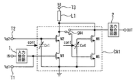
図1は、本発明の実施の形態1に係るカスコードアンプを示す回路図である。トランジスタM1、M2はnチャネルMOSトランジスタである。入力端子INにはRF入力信号が入力され、出力端子OUTからRF出力信号が出力される。バイアス端子T1,T2にはそれぞれバイアスVg1,Vg2が供給される。電源端子T3は電源に接続される。
FIG. 1 is a circuit diagram showing a cascode amplifier according to
トランジスタM1のゲートは、入力整合回路1を介して入力端子INに接続され、かつバイアス端子T1に接続される。トランジスタM1のソースは接地されている。従って、トランジスタM1はソース接地アンプである。トランジスタM2のゲートはバイアス端子T2に接続され、ソースはトランジスタM1のドレインに接続されている。トランジスタM2のドレインはフィードラインL1を介して電源端子T3に接続され、かつ出力整合回路2を介して出力端子OUTに接続されている。フィードラインL1は特定の電気長を有する線路でインダクタとして作用する。
The gate of the transistor M1 is connected to the input terminal IN through the
トランジスタM2のゲートと接地点との間に可変容量Cv1が接続されている。従って、トランジスタM2は、ゲートが可変容量Cv1を介して高周波的に接地されたゲート接地アンプである。トランジスタM1とトランジスタM2はカスコード接続されている。トランジスタM1,M2と可変容量Cv1がカスコードアンプCA1を構成する(図1の点線枠内)。 A variable capacitor Cv1 is connected between the gate of the transistor M2 and the ground point. Therefore, the transistor M2 is a grounded-gate amplifier whose gate is grounded in high frequency via the variable capacitor Cv1. The transistors M1 and M2 are cascode-connected. The transistors M1 and M2 and the variable capacitor Cv1 constitute a cascode amplifier CA1 (within the dotted frame in FIG. 1).
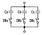
図2は、本発明の実施の形態1に係る可変容量を示す回路図である。固定容量Ca,Cb,Ccが互いに並列に接続され、それらにそれぞれスイッチSWa,SWb,SWcが直列に接続されている。固定容量Ca,Cb,CcはCMOSプロセスで得られるMOS容量である。スイッチSWa,SWb,SWcを切り替えることで容量値を調整することができる。 FIG. 2 is a circuit diagram showing the variable capacitor according to the first embodiment of the present invention. Fixed capacitors Ca, Cb, and Cc are connected in parallel with each other, and switches SWa, SWb, and SWc are connected in series with each other. Fixed capacitors Ca, Cb, and Cc are MOS capacitors obtained by a CMOS process. The capacitance value can be adjusted by switching the switches SWa, SWb, and SWc.
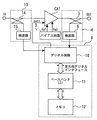
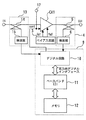
図3は、本発明の実施の形態1に係る電力増幅器を示す回路図である。バイアス回路3はバイアス端子T1,T2にそれぞれバイアスVg1,Vg2を供給する。出力電力検知回路4は、電力増幅器の出力線路に設けられた方向性結合器5と、その方向性結合器5に接続された検波器6とを有する。出力電力検知回路4は、カスコードアンプCA1から出力された出力信号の電力を検知して電気信号に変換する。
FIG. 3 is a circuit diagram showing the power amplifier according to
発振器7がスイッチ8を介してカスコードアンプCA1の入力に接続されている。この発振器7とスイッチ8がBIST(Built-in self test)を構成する。制御回路9のデジタル回路10がスイッチ8をオンし発振器7を起動することで、発振器7は既知の数ポイントの入力電力を持つテスト信号を発生してカスコードアンプCA1に入力させる。出力電力検知回路4は、カスコードアンプCA1から出力された出力信号の電力を検知する。デジタル回路10は、既知の数ポイントの入力電力と検知した出力電力に基づいて電力増幅器の初期の利得(異なる数ポイントの利得)を求める。
The
デジタル回路10は、求めた初期の利得を、デジタルインターフェイスを介してベースバンドLSI11に送信する。ベースバンドLSI11は、予め設定値として内部に保持する所望の利得と、デジタル回路10が求めた初期の利得とを比較することで、デジタルインターフェイスを介して利得の増減指令をデジタル回路10へ伝送する。メモリ12は、所望の容量値にセットするために必要な情報を保持する。デジタル回路10は、カスコードアンプCA1の利得が所望の値になるように可変容量Cv1の制御電圧contを決定し、可変容量Cv1の容量値を制御する。
The
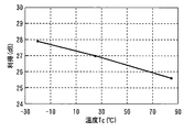
図4は、可変容量の容量値とカスコードアンプの利得の関係を示す図である。主に携帯電話の送信周波数に用いられる700MHz〜2GHzの帯域においては可変容量Cv1の容量値が大きいほど利得が高くなることがわかる。この関係性を利用し、電圧制御などで可変容量Cv1の容量値を変化させることにより電力増幅器の歪特性(ACLR)など他の特性への影響を与えることなく利得のみを調整することができる。 FIG. 4 is a diagram showing the relationship between the capacitance value of the variable capacitor and the gain of the cascode amplifier. It can be seen that the gain increases as the capacitance value of the variable capacitor Cv1 increases in the band of 700 MHz to 2 GHz mainly used for the transmission frequency of the mobile phone. By using this relationship and changing the capacitance value of the variable capacitor Cv1 by voltage control or the like, it is possible to adjust only the gain without affecting other characteristics such as the distortion characteristic (ACLR) of the power amplifier.
本実施の形態では、カスコードアンプCA1の利得が初期状態から所望の値になるように可変容量Cv1の容量値を制御する。これにより、トランジスタの動作級などの他の特性を変化させることなく利得を調整することができる。このため、電力増幅器内の能動素子や受動素子の製造ばらつきに起因する歪みばらつきを抑制することができる。 In the present embodiment, the capacitance value of the variable capacitor Cv1 is controlled so that the gain of the cascode amplifier CA1 becomes a desired value from the initial state. Thereby, the gain can be adjusted without changing other characteristics such as the operation class of the transistor. For this reason, the distortion dispersion | variation resulting from the manufacture dispersion | variation in the active element in a power amplifier and a passive element can be suppressed.
なお、本実施の形態では利得調整機能のない増幅器は省略しているが、電力増幅器は多段構成でもよく、利得調整機能のあるカスコードアンプを複数段設けてもよい。 Although an amplifier without a gain adjustment function is omitted in this embodiment, the power amplifier may have a multistage configuration, and a plurality of cascode amplifiers with a gain adjustment function may be provided.
実施の形態2.
図5は、本発明の実施の形態2に係る電力増幅器を示す回路図である。実施の形態1の発振器7とスイッチ8の代わりに入力電力検知回路13が設けられている。入力電力検知回路13は、電力増幅器の入力線路に設けられた方向性結合器14と、その方向性結合器14に接続された検波器15とを有する。入力電力検知回路13は、カスコードアンプCA1に入力される入力信号の電力を検知する。制御回路9は、入力信号の電力と出力信号の電力から利得を求め、この求めた利得が任意の動作状態において所望の値になるように可変容量Cv1の容量値を制御する。
FIG. 5 is a circuit diagram showing a power amplifier according to
携帯電話などの移動体端末において、受信帯域雑音という利得と相関が見られる重要な特性がある。図6は、受信帯域雑音と利得の関係を示す図である。高周波電力増幅器の受信帯域雑音が大きくなる出力電力が大きな場合においてのみ、電力増幅器の利得を規格値内で低下させるように調整することで、受信帯域雑音を改善することができる。 In a mobile terminal such as a mobile phone, there is an important characteristic that is correlated with a gain called reception band noise. FIG. 6 is a diagram showing the relationship between reception band noise and gain. Only when the output power at which the reception band noise of the high-frequency power amplifier becomes large is large, the reception band noise can be improved by adjusting the gain of the power amplifier to fall within the standard value.
実施の形態3.
図7は、本発明の実施の形態3に係るカスコードアンプを示す回路図である。ゲート幅の異なるトランジスタM2,M3,M4が並列に接続されている。トランジスタM2,M3,M4のゲートと接地点の間にそれぞれ可変容量Cv1,Cv2,Cv3が接続されている。また、トランジスタM2,M3,M4のソースとトランジスタM1のドレインとの間にそれぞれスイッチSW1,SW2,SW3が接続されている。
FIG. 7 is a circuit diagram showing a cascode amplifier according to
ゲート幅の異なるトランジスタM2,M3,M4をスイッチSW1,SW2,SW3で切り替え選択することにより、利得の調整範囲を広げるだけでなく、カスコードアンプの出力電力も調整することができ、用途に応じて使い分けることができる。 By selecting and switching the transistors M2, M3, and M4 having different gate widths with the switches SW1, SW2, and SW3, not only the gain adjustment range can be expanded, but also the output power of the cascode amplifier can be adjusted. Can be used properly.
なお、ここではゲート接地トランジスタを3個配置しているが、ゲート接地トランジスタが複数であればよく、数は問わない。また、トランジスタM2,M3,M4のゲート幅サイズが異なっていれば利得や出力電力の調整範囲を広くできるが、これらのゲート幅サイズは同一であってもよい。 Here, although three grounded gate transistors are arranged, it is sufficient that there are a plurality of grounded gate transistors, and the number is not limited. Further, if the gate width sizes of the transistors M2, M3, and M4 are different, the adjustment range of the gain and output power can be widened, but these gate width sizes may be the same.
図8は、本発明の実施の形態3に係るスイッチSW1,SW2,SW3を示す回路図である。トランジスタTr1のドレインDにドレインバイアスVdが印加され、ゲートにゲート抵抗R1を介してゲートバイアスVg1が印加されると、ドレインDとソースSの間が導通する。 FIG. 8 is a circuit diagram showing the switches SW1, SW2, and SW3 according to the third embodiment of the present invention. When the drain bias Vd is applied to the drain D of the transistor Tr1 and the gate bias Vg1 is applied to the gate via the gate resistance R1, the drain D and the source S are brought into conduction.
図9は、本発明の実施の形態3に係る電力増幅器を示す回路図である。制御回路9は、スイッチSW1,SW2,SW3を制御して、ゲート幅の異なるトランジスタM2,M3,M4の1つを選択してトランジスタM1に接続する。これにより、高周波電力増幅器の利得だけでなく、出力電力も所望の値に制御することができる。
FIG. 9 is a circuit diagram showing a power amplifier according to
携帯電話などの移動体端末において、アンテナのインピーダンスは移動体端末の使用状況により変化する。以前は送信電力増幅器の出力端子からアンテナまでの経路にアイソレータが設けられていたため、アンテナのインピーダンスが変化しても送信電力増幅器の出力負荷インピーダンスは所定のインピーダンス(例えば50Ω)に固定されていた。しかし、小型化、低コスト化のため近年はアイソレータを配置しないため、アンテナのインピーダンスの変化に伴い送信電力増幅器の出力負荷インピーダンスは変化する。 In a mobile terminal such as a mobile phone, the impedance of the antenna varies depending on the usage status of the mobile terminal. Previously, since an isolator was provided in the path from the output terminal of the transmission power amplifier to the antenna, the output load impedance of the transmission power amplifier was fixed to a predetermined impedance (for example, 50Ω) even when the impedance of the antenna changed. However, since the isolator is not arranged in recent years for miniaturization and cost reduction, the output load impedance of the transmission power amplifier changes with the change of the impedance of the antenna.
図10は、本発明の実施の形態3に係る電力増幅器の利得の負荷依存性を示す図である。本実施の形態により負荷変動に対する高周波電力増幅器の利得の変動量を補償することができるため、任意の出力負荷インピーダンスにおいて一定の利得を得ることができる。 FIG. 10 is a diagram showing the load dependence of the gain of the power amplifier according to the third embodiment of the present invention. According to the present embodiment, the amount of fluctuation in the gain of the high-frequency power amplifier with respect to the load fluctuation can be compensated, so that a constant gain can be obtained at any output load impedance.
実施の形態4.
図11は、本発明の実施の形態4に係るカスコードアンプを示す回路図である。トランジスタM1,M2及び可変容量Cv1からなる前段のカスコードアンプの後に、トランジスタM5,M6及び可変容量Cv4からなる後段のカスコードアンプがスイッチSW4を介して接続されている。なお、本実施の形態ではカスコードアンプを2段配置しているが、カスコードアンプの段数は問わない。
FIG. 11 is a circuit diagram showing a cascode amplifier according to
図12は、本発明の実施の形態4に係るスイッチSW4を示す回路図である。トランジスタTr2のドレインDにドレインバイアスVdが印加され、ゲートにゲート抵抗R2を介してゲートバイアスVg2が印加されると、ドレインDとソースS1との間が導通する。トランジスタTr3のドレインDにドレインバイアスVdが印加され、ゲートにゲート抵抗R3を介してゲートバイアスVg3が印加されるとドレインDとソースS2との間が導通する。 FIG. 12 is a circuit diagram showing the switch SW4 according to the fourth embodiment of the present invention. When the drain bias Vd is applied to the drain D of the transistor Tr2 and the gate bias Vg2 is applied to the gate via the gate resistor R2, the drain D and the source S1 are electrically connected. When the drain bias Vd is applied to the drain D of the transistor Tr3 and the gate bias Vg3 is applied to the gate via the gate resistor R3, the drain D and the source S2 are brought into conduction.
電力増幅器を示す回路図は実施の形態1と同様であるが、制御回路9がスイッチSW4も制御する点が異なる。本実施の形態では、制御回路9は、スイッチSW4を制御して、前段のカスコードアンプを後段のカスコードアンプに接続させるかどうかを切り替える。これにより、前段のカスコードアンプの単段経路と、前段と後段のカスコードアンプの多段経路の何れかを選択することができるため、利得調整範囲を拡大することができる。
The circuit diagram showing the power amplifier is the same as that of the first embodiment except that the
実施の形態5.
図13は、本発明の実施の形態5に係る電力増幅器を示す回路図である。出力線路LOUTがカスコードアンプCA1の出力に接続されている。温度検知回路16は出力線路LOUTの温度を検知する。制御回路9は、検知された温度に応じて可変容量Cv1の容量値を制御して利得が所望の値になるようにする。具体的には、制御回路9のデジタル回路10は、メモリ12に予め設定された温度特性データと検知された温度に基づいて可変容量Cv1の容量値を所望の値にセットし、温度変化に対し利得が所望の値になるようにする。
FIG. 13 is a circuit diagram showing a power amplifier according to the fifth embodiment of the present invention. The output line L OUT is connected to the output of the cascode amplifier CA1. The
図14は、可変容量の容量値が一定の場合の温度変化に対する利得を示す図である。温度変化に伴って利得が変化する。そこで、本実施の形態では温度変化に伴う利得の変化を補償することで、温度変化に対する利得の変動を抑制することができる。また、ある温度において任意の利得に調整することもできる。 FIG. 14 is a diagram illustrating a gain with respect to a temperature change when the capacitance value of the variable capacitor is constant. The gain changes with temperature change. Therefore, in this embodiment, by compensating for the gain change accompanying the temperature change, the gain fluctuation with respect to the temperature change can be suppressed. It can also be adjusted to an arbitrary gain at a certain temperature.
実施の形態6.
図15は、本発明の実施の形態6に係る電力増幅器を示す回路図である。可変容量Cv1の容量値を電圧制御する制御信号が供給される外部端子17が設けられている。これにより、通信機器用端末基板上に実装後でもユーザーが可変容量Cv1の容量値を外部から直接調整して、高周波電力増幅器の利得を所望の値に調整することができる。従って、ユーザーの調整によって1つの高周波電力増幅器で異なる利得が得られるため、高周波電力増幅器の品種のバリエーションを抑えられ、開発効率を改善することができる。
FIG. 15 is a circuit diagram showing a power amplifier according to the sixth embodiment of the present invention. An
4 出力電力検知回路、7 発振器、9 制御回路、13 入力電力検知回路、16 温度検知回路、17 外部端子、Cv1 可変容量、CA1,CA2 カスコードアンプ、M1,M5 トランジスタ(第1のトランジスタ)、M2,M3,M4,M6 トランジスタ(第2のトランジスタ)、T1 バイアス端子(第1のバイアス端子)、T2 バイアス端子(第2のバイアス端子) 4 Output power detection circuit, 7 Oscillator, 9 Control circuit, 13 Input power detection circuit, 16 Temperature detection circuit, 17 External terminal, Cv1 variable capacitor, CA1, CA2 Cascode amplifier, M1, M5 transistor (first transistor), M2 , M3, M4, M6 transistor (second transistor), T1 bias terminal (first bias terminal), T2 bias terminal (second bias terminal)
Claims (8)
前記第1のバイアス端子に接続された第1の制御端子と、接地された第1の端子と、第2の端子とを有する第1のトランジスタと、
前記第2のバイアス端子に接続された第2の制御端子と、前記第2の端子に接続された第3の端子と、第4の端子とを有する第2のトランジスタと、
前記第2の制御端子と接地点との間に接続された可変容量とを備えることを特徴とする電力増幅器。 First and second bias terminals to which a bias is supplied, respectively;
A first transistor having a first control terminal connected to the first bias terminal, a grounded first terminal, and a second terminal;
A second transistor having a second control terminal connected to the second bias terminal, a third terminal connected to the second terminal, and a fourth terminal;
A power amplifier comprising: a variable capacitor connected between the second control terminal and a ground point.
前記カスコードアンプの利得が所望の値になるように前記可変容量の容量値を制御する制御回路を更に備えることを特徴とする請求項1に記載の電力増幅器。 The first and second transistors and the variable capacitor constitute a cascode amplifier,
The power amplifier according to claim 1, further comprising a control circuit that controls a capacitance value of the variable capacitor so that a gain of the cascode amplifier becomes a desired value.
前記カスコードアンプから出力された出力信号の電力を検知する出力電力検知回路とを更に備え、
前記制御回路は、前記テスト信号の電力と前記出力信号の電力から前記利得を求め、この求めた前記利得が所望の値になるように前記可変容量の容量値を制御することを特徴とする請求項2に記載の電力増幅器。 An oscillator for supplying a test signal to the input of the cascode amplifier;
An output power detection circuit for detecting the power of the output signal output from the cascode amplifier,
The control circuit obtains the gain from the power of the test signal and the power of the output signal, and controls the capacitance value of the variable capacitor so that the obtained gain becomes a desired value. Item 3. The power amplifier according to Item 2.
前記カスコードアンプから出力された出力信号の電力を検知する出力電力検知回路とを更に備え、
前記制御回路は、前記入力信号の電力と前記出力信号の電力から前記利得を求め、この求めた前記利得が所望の値になるように前記可変容量の容量値を制御することを特徴とする請求項2に記載の電力増幅器。 An input power detection circuit for detecting power of an input signal input to the cascode amplifier;
An output power detection circuit for detecting the power of the output signal output from the cascode amplifier,
The control circuit obtains the gain from the power of the input signal and the power of the output signal, and controls the capacitance value of the variable capacitor so that the obtained gain becomes a desired value. Item 3. The power amplifier according to Item 2.
前記制御回路は、前記複数のトランジスタの1つを選択して前記第1のトランジスタに接続することを特徴とする請求項2〜4の何れか1項に記載の電力増幅器。 The second transistor has a plurality of transistors having different gate widths,
5. The power amplifier according to claim 2, wherein the control circuit selects one of the plurality of transistors and connects the selected transistor to the first transistor. 6.
前記制御回路は、前記前段のカスコードアンプを前記後段のカスコードアンプに接続させるかどうかを切り替えることを特徴とする請求項2〜4の何れか1項に記載の電力増幅器。 The cascode amplifier has a cascode amplifier at the front stage and a cascode amplifier at the rear stage,
5. The power amplifier according to claim 2, wherein the control circuit switches whether to connect the front-stage cascode amplifier to the rear-stage cascode amplifier. 6.
前記出力線路の温度を検知する温度検知回路とを更に備え、
前記制御回路は、検知された前記温度に応じて前記可変容量の容量値を制御することを特徴とする請求項2に記載の電力増幅器。 An output line connected to the output of the cascode amplifier;
A temperature detection circuit for detecting the temperature of the output line,
The power amplifier according to claim 2, wherein the control circuit controls a capacitance value of the variable capacitor in accordance with the detected temperature.
Priority Applications (1)
| Application Number | Priority Date | Filing Date | Title |
|---|---|---|---|
| JP2013085783A JP6372030B2 (en) | 2013-04-16 | 2013-04-16 | Power amplifier |
Applications Claiming Priority (1)
| Application Number | Priority Date | Filing Date | Title |
|---|---|---|---|
| JP2013085783A JP6372030B2 (en) | 2013-04-16 | 2013-04-16 | Power amplifier |
Publications (2)
| Publication Number | Publication Date |
|---|---|
| JP2014209672A true JP2014209672A (en) | 2014-11-06 |
| JP6372030B2 JP6372030B2 (en) | 2018-08-15 |
Family
ID=51903639
Family Applications (1)
| Application Number | Title | Priority Date | Filing Date |
|---|---|---|---|
| JP2013085783A Active JP6372030B2 (en) | 2013-04-16 | 2013-04-16 | Power amplifier |
Country Status (1)
| Country | Link |
|---|---|
| JP (1) | JP6372030B2 (en) |
Cited By (1)
| Publication number | Priority date | Publication date | Assignee | Title |
|---|---|---|---|---|
| CN115694383A (en) * | 2022-12-29 | 2023-02-03 | 广州慧智微电子股份有限公司 | Amplifier and multistage amplifier |
Citations (8)
| Publication number | Priority date | Publication date | Assignee | Title |
|---|---|---|---|---|
| JPH01123512A (en) * | 1987-11-09 | 1989-05-16 | Nec Corp | Temperature change follow-up type agc device |
| JPH10132883A (en) * | 1996-11-01 | 1998-05-22 | Shimada Phys & Chem Ind Co Ltd | Monitoring method and monitoring controller for amplifier characteristics |
| JP2003092523A (en) * | 2001-07-11 | 2003-03-28 | Fujitsu Ltd | Cascade type distributed amplifier |
| JP2007259297A (en) * | 2006-03-24 | 2007-10-04 | Sharp Corp | Variable gain amplifier and communication equipment provided with the variable gain amplifier |
| JP2009505517A (en) * | 2005-08-11 | 2009-02-05 | ビットウェーブ・セミコンダクター・インコーポレイテッド | Programmable radio transceiver |
| JP2009200958A (en) * | 2008-02-22 | 2009-09-03 | Asahi Kasei Electronics Co Ltd | Amplifier |
| JP2011229083A (en) * | 2010-04-22 | 2011-11-10 | Renesas Electronics Corp | Wireless communication device, wireless communication method, and program |
| JP2013038772A (en) * | 2011-07-12 | 2013-02-21 | Mitsubishi Electric Corp | Nonlinear characteristic analyzer and transmitter |
-
2013
- 2013-04-16 JP JP2013085783A patent/JP6372030B2/en active Active
Patent Citations (8)
| Publication number | Priority date | Publication date | Assignee | Title |
|---|---|---|---|---|
| JPH01123512A (en) * | 1987-11-09 | 1989-05-16 | Nec Corp | Temperature change follow-up type agc device |
| JPH10132883A (en) * | 1996-11-01 | 1998-05-22 | Shimada Phys & Chem Ind Co Ltd | Monitoring method and monitoring controller for amplifier characteristics |
| JP2003092523A (en) * | 2001-07-11 | 2003-03-28 | Fujitsu Ltd | Cascade type distributed amplifier |
| JP2009505517A (en) * | 2005-08-11 | 2009-02-05 | ビットウェーブ・セミコンダクター・インコーポレイテッド | Programmable radio transceiver |
| JP2007259297A (en) * | 2006-03-24 | 2007-10-04 | Sharp Corp | Variable gain amplifier and communication equipment provided with the variable gain amplifier |
| JP2009200958A (en) * | 2008-02-22 | 2009-09-03 | Asahi Kasei Electronics Co Ltd | Amplifier |
| JP2011229083A (en) * | 2010-04-22 | 2011-11-10 | Renesas Electronics Corp | Wireless communication device, wireless communication method, and program |
| JP2013038772A (en) * | 2011-07-12 | 2013-02-21 | Mitsubishi Electric Corp | Nonlinear characteristic analyzer and transmitter |
Cited By (1)
| Publication number | Priority date | Publication date | Assignee | Title |
|---|---|---|---|---|
| CN115694383A (en) * | 2022-12-29 | 2023-02-03 | 广州慧智微电子股份有限公司 | Amplifier and multistage amplifier |
Also Published As
| Publication number | Publication date |
|---|---|
| JP6372030B2 (en) | 2018-08-15 |
Similar Documents
| Publication | Publication Date | Title |
|---|---|---|
| US8093952B2 (en) | Method and system for precise current matching in deep sub-micron technology | |
| US10797662B2 (en) | Amplifying circuit including miller compensation circuit | |
| JP5831511B2 (en) | High frequency power amplifier | |
| US8395448B2 (en) | Apparatus and method for miller compensation for multi-stage amplifier | |
| EP2946467B1 (en) | Amplifier with switchable common gate gain buffer | |
| KR101654221B1 (en) | Power amplifier | |
| US8183843B2 (en) | Voltage regulator and associated methods | |
| US11290060B2 (en) | Bias circuit | |
| US9294053B2 (en) | Amplifying circuit including active inductor | |
| KR20200005465A (en) | Amplifier linearity boost circuits and methods for post distortion feedback cancelation | |
| US20140128013A1 (en) | Low variation current multiplier | |
| US8031002B2 (en) | Buffer amplifier | |
| JP6372030B2 (en) | Power amplifier | |
| WO2008044750A1 (en) | Low-noise amplifier | |
| US20230030709A1 (en) | Broadband low noise amplifier using multiple cascode stages | |
| US9072044B2 (en) | Push-pull amplifier with quiescent current adjuster | |
| WO2012156947A1 (en) | Amplifier | |
| CN109525211B (en) | Amplifier and wireless signal receiver including the same | |
| GB2490977A (en) | A configurable LNA with inductive degeneration or with an impedance-matching stage in parallel with the principal gain stage | |
| US20120049941A1 (en) | Apparatus and method configured to provide electrical bias | |
| CN117395761B (en) | Power supply and bias adjustable radio frequency front end module and radio frequency chip | |
| KR101145347B1 (en) | Low noise amplifier and gain control circuit for amplifier | |
| US7053716B2 (en) | Controlled impedance bias circuit | |
| JP2006339837A (en) | Circuit integration high frequency amplifier | |
| US20200186101A1 (en) | Amplification circuit |
Legal Events
| Date | Code | Title | Description |
|---|---|---|---|
| A621 | Written request for application examination |
Free format text: JAPANESE INTERMEDIATE CODE: A621 Effective date: 20160119 |
|
| A977 | Report on retrieval |
Free format text: JAPANESE INTERMEDIATE CODE: A971007 Effective date: 20170127 |
|
| A131 | Notification of reasons for refusal |
Free format text: JAPANESE INTERMEDIATE CODE: A131 Effective date: 20170207 |
|
| A521 | Request for written amendment filed |
Free format text: JAPANESE INTERMEDIATE CODE: A523 Effective date: 20170303 |
|
| A131 | Notification of reasons for refusal |
Free format text: JAPANESE INTERMEDIATE CODE: A131 Effective date: 20171003 |
|
| A521 | Request for written amendment filed |
Free format text: JAPANESE INTERMEDIATE CODE: A523 Effective date: 20171102 |
|
| TRDD | Decision of grant or rejection written | ||
| A01 | Written decision to grant a patent or to grant a registration (utility model) |
Free format text: JAPANESE INTERMEDIATE CODE: A01 Effective date: 20180605 |
|
| A711 | Notification of change in applicant |
Free format text: JAPANESE INTERMEDIATE CODE: A711 Effective date: 20180628 |
|
| A61 | First payment of annual fees (during grant procedure) |
Free format text: JAPANESE INTERMEDIATE CODE: A61 Effective date: 20180628 |
|
| R150 | Certificate of patent or registration of utility model |
Ref document number: 6372030 Country of ref document: JP Free format text: JAPANESE INTERMEDIATE CODE: R150 |