JP2009200958A - Amplifier - Google Patents
Amplifier Download PDFInfo
- Publication number
- JP2009200958A JP2009200958A JP2008041992A JP2008041992A JP2009200958A JP 2009200958 A JP2009200958 A JP 2009200958A JP 2008041992 A JP2008041992 A JP 2008041992A JP 2008041992 A JP2008041992 A JP 2008041992A JP 2009200958 A JP2009200958 A JP 2009200958A
- Authority
- JP
- Japan
- Prior art keywords
- transistor
- amplifier
- impedance control
- power supply
- positive power
- Prior art date
- Legal status (The legal status is an assumption and is not a legal conclusion. Google has not performed a legal analysis and makes no representation as to the accuracy of the status listed.)
- Pending
Links
Images


Abstract
Description
本発明は、増幅器に関し、より詳細には、可変利得の増幅器に関する。 The present invention relates to amplifiers, and more particularly to variable gain amplifiers.
可変利得の増幅器であるギルバート掛け算器回路(Gilbert Multiplier)が、従来高周波帯で用いられてきた(非特許文献1および2参照)。ギルバート掛け算器回路の一例を図8に示す。入力RF信号振幅VRFのAC入力がトランジスタQ1、Q2に与えられ、入力直流電圧VLOのDC入力がトランジスタQM1〜QM4に与えられる。COMは基準電位端子であり、VPOSは正電源電位端子である。得られるAC出力の出力RF信号振幅は、VRF×VLOに比例する。このようにギルバート掛け算器回路では、「(DC入力)×(AC入力)=(AC出力)」という掛け算を実行でき、DC入力に比例したAC出力が得られる。したがって、DC入力によってAC入力の利得を可変させることができる。
A Gilbert multiplier circuit, which is a variable gain amplifier, has been conventionally used in a high frequency band (see Non-Patent
しかしながら、ギルバート掛け算器回路では(符号は以下の説明の通り。)、IC(Q1)+IC(Q2)=Izは常に成立するものの、IC(QM1)+IC(QM2)=IC(QM3)+IC(QM4)はVLO平衡状態以外では成立せず、VC(Q1)=VC(Q2)も成立しない。言い換えると、ギルバート掛け算回路を用いた可変利得増幅器では、VLOを利得制御のパラメータとするのでAC入力の通過する系に存在するトランジスタQ1およびQ2の直流バイアス条件を変えてしまう。したがって、AC入力に対する歪率も変ってしまい、歪に対する最適化が困難になるという問題があった。 However, in the Gilbert multiplier circuit (the sign is as described below), IC (Q1) + IC (Q2) = Iz always holds, but IC (QM1) + IC (QM2) = IC (QM3) + IC (QM4) ) Does not hold except in the VLO equilibrium state, and VC (Q1) = VC (Q2) does not hold. In other words, in a variable gain amplifier using a Gilbert multiplication circuit, V LO is used as a gain control parameter, and therefore the DC bias conditions of the transistors Q1 and Q2 existing in the system through which the AC input passes are changed. Therefore, the distortion rate with respect to the AC input also changes, and there is a problem that optimization for distortion becomes difficult.
符号の説明
IC(Q1);トランジスタQ1のコレクタ電流
IC(Q2);トランジスタQ2のコレクタ電流
Iz;トランジスタQCのコレクタ電流
IC(QM1);トランジスタQM1のコレクタ電流
IC(QM2);トランジスタQM2のコレクタ電流
IC(QM3);トランジスタQM3のコレクタ電流
IC(QM4);トランジスタQM4のコレクタ電流
VC(Q1);トランジスタQ1のコレクタ電圧
VC(Q2);トランジスタQ2のコレクタ電圧
Description of symbols IC (Q1); collector current IC (Q2) of transistor Q1; collector current Iz of transistor Q2; collector current IC (QM1) of transistor QC; collector current IC (QM2) of transistor QM1; collector current of transistor QM2 IC (QM3); collector current IC (QM4) of transistor QM3; collector current VC (Q1) of transistor QM4; collector voltage VC (Q2) of transistor Q1; collector voltage of transistor Q2
本発明は、このような問題点に鑑みてなされたものであり、その目的は、AC入力の歪率を変化させることなく利得が可変可能である増幅器を提供することにある。 The present invention has been made in view of such problems, and an object thereof is to provide an amplifier whose gain can be varied without changing the distortion factor of the AC input.
このような問題を解決するために、請求項1に記載の発明は、AC入力が入力されるトランジスタおよび前記トランジスタのドレイン端子側に接続された負荷を備える増幅器であって、基準電位と前記トランジスタのソース端子側とを接続する第1の接続線、および正電源電位と前記トランジスタのドレイン端子側とを接続する第2の接続線のうちの少なくとも一方のインピーダンスを制御するインピーダンス制御回路を備えることを特徴とする。
In order to solve such a problem, the invention according to
また、請求項2に記載の発明は、請求項1において、前記インピーダンス制御回路は、インダクタンス素子および前記インダクタンス素子に直列に接続されるスイッチで構成されるインピーダンス制御素子が複数並列に接続されており、前記基準電位と前記トランジスタのソース端子との間、または前記正電源電位と前記トランジスタのドレイン端子との間の少なくとも一方に配置されていることを特徴とする。 According to a second aspect of the present invention, in the first aspect, the impedance control circuit includes a plurality of impedance control elements connected in parallel, each of which includes an inductance element and a switch connected in series to the inductance element. , Being arranged between at least one of the reference potential and the source terminal of the transistor, or between the positive power supply potential and the drain terminal of the transistor.
また、請求項3に記載の発明は、請求項1において、前記インピーダンス制御回路は、前記第1の接続線と前記第2の接続線との間に配置された可変容量であることを特徴とする。 According to a third aspect of the present invention, in the first aspect, the impedance control circuit is a variable capacitor disposed between the first connection line and the second connection line. To do.
また、請求項4に記載の発明は、請求項2において、前記第1の接続線と前記第2の接続線との間に配置された可変容量をさらに備えることを特徴とする。 According to a fourth aspect of the present invention, in the second aspect of the present invention, the apparatus further includes a variable capacitor disposed between the first connection line and the second connection line.
本発明によれば、基準電位または正電源電位の少なくとも一方と増幅器とを接続する接続線のインピーダンスを制御するインピーダンス制御回路を設けることにより、AC入力の歪率を変化させることなく利得が可変可能である増幅器を提供することができる。 According to the present invention, by providing an impedance control circuit for controlling the impedance of a connection line connecting at least one of the reference potential or the positive power supply potential and the amplifier, the gain can be varied without changing the distortion factor of the AC input. An amplifier can be provided.
以下、図面を参照して本発明の実施形態を詳細に説明する。
(第1の実施形態)
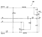
図1は、第1の実施形態に係る増幅器を示している。増幅器100は、ソース接地の第1のトランジスタM1を備える。AC入力入力端子INが、直流阻止容量C1の一方の端子に接続され、直流阻止容量C1の他方の端子が、抵抗RBおよびインダクタLINの一方の端子に接続される。抵抗RBは、トランジスタM1の入力容量をキャンセルし、インダクタLINは、トランジスタM1の直流動作点を決定する。
Hereinafter, embodiments of the present invention will be described in detail with reference to the drawings.
(First embodiment)
FIG. 1 shows an amplifier according to the first embodiment. The
抵抗RBの他方の端子が、第2のトランジスタM2のゲート端子およびドレイン端子、ならびに直流バイアス電流入力端子IBに接続される。第2のトランジスタM2のソース端子およびバルク端子が、増幅器基準電位VSS1P8Iに接続される。 The other terminal of the resistor RB is connected to the gate terminal and drain terminal of the second transistor M2 and the DC bias current input terminal IB. The source terminal and bulk terminal of the second transistor M2 are connected to the amplifier reference potential VSS1P8I.
インダクタLINの他方の端子が、第1のトランジスタM1のゲート端子に接続される。トランジスタM1のソース端子が、ソース・ディジェネレイション用のインダクタLSを介して増幅器基準電位VSS1P8Iに接続され、トランジスタM1のドレイン端子が、カスコードトランジスタMC1のソース端子に接続される。カスコードトランジスタMC1のゲート端子が、増幅器正電源電位VDD1P8Iに接続され、ドレイン端子は、負荷インダクタンスLLを介して増幅器正電源電位VDD1P8Iに接続される。増幅器100の出力は、カスコードトランジスタMC1のドレイン端子と負荷LLの接続点である出力端子OUTから取り出される。
The other terminal of the inductor LIN is connected to the gate terminal of the first transistor M1. The source terminal of the transistor M1 is connected to the amplifier reference potential VSS1P8I via the source degeneration inductor LS, and the drain terminal of the transistor M1 is connected to the source terminal of the cascode transistor MC1. The gate terminal of the cascode transistor MC1 is connected to the amplifier positive power supply potential VDD1P8I, and the drain terminal is connected to the amplifier positive power supply potential VDD1P8I via the load inductance LL. The output of the
増幅器基準電位VSS1P8Iと基準電位VSS1P8との間のインピーダンスは、図1に示したように、インダクタンス素子L1S及びそれに直列に接続されるスイッチS1Sで構成される第1の基準電位側インピーダンス制御素子と、インダクタンスL2S及びスイッチS2Sで構成される第2の基準電位側インピーダンス制御素子と、インダクタンスL3S及びスイッチS3Sで構成される第3の基準電位側インピーダンス制御素子と、インダクタンスL4S及びスイッチS4Sで構成される第4の基準電位側インピーダンス制御素子とにより制御される。ここで、第2から第4の基準電位側インピーダンス制御素子は、第1の基準電位側インピーダンス制御素子と並列に接続されている。第1から第4の基準電位側インピーダンス制御素子を併せて、基準電位側インピーダンス制御回路と呼ぶ。 As shown in FIG. 1, the impedance between the amplifier reference potential VSS1P8I and the reference potential VSS1P8 includes an inductance element L1S and a first reference potential side impedance control element configured by a switch S1S connected in series thereto, A second reference potential side impedance control element composed of an inductance L2S and a switch S2S, a third reference potential side impedance control element composed of an inductance L3S and a switch S3S, and a second reference potential side impedance control element composed of an inductance L4S and a switch S4S. 4 is controlled by the reference potential side impedance control element. Here, the second to fourth reference potential side impedance control elements are connected in parallel with the first reference potential side impedance control element. The first to fourth reference potential side impedance control elements are collectively referred to as a reference potential side impedance control circuit.
また、増幅器正電源電位VDD1P8Iと正電源電位VDD1P8との間のインピーダンスは、インダクタンスL1D及びそれに直列接続されるスイッチS1Dで構成される第1の正電源電位側インピーダンス制御素子と、インダクタンスL2D及びスイッチS2Dで構成される第2の正電源電位側インピーダンス制御素子と、インダクタンスL3D及びスイッチS3Dで構成される第3の正電源電位側インピーダンス制御素子と、インダクタンスL4D及びスイッチS4Dで構成される第4の正電源電位側インピーダンス制御素子により制御される。ここで、第2から第4の正電源電位側インピーダンス制御素子は、第1の正電源電位側インピーダンス制御素子と並列に接続されている。第1から第4の正電源電位側インピーダンス制御素子を併せて、正電源電位側インピーダンス制御回路と呼ぶ。 In addition, the impedance between the amplifier positive power supply potential VDD1P8I and the positive power supply potential VDD1P8 is the first positive power supply potential side impedance control element including the inductance L1D and the switch S1D connected in series thereto, the inductance L2D, and the switch S2D. A second positive power supply potential side impedance control element constituted by the third positive power supply potential side impedance control element constituted by the inductance L3D and the switch S3D, and a fourth positive power supply constituted by the inductance L4D and the switch S4D. It is controlled by the power supply potential side impedance control element. Here, the second to fourth positive power supply potential side impedance control elements are connected in parallel with the first positive power supply potential side impedance control element. The first to fourth positive power supply potential side impedance control elements are collectively referred to as a positive power supply potential side impedance control circuit.
第1の実施形態に係る増幅器100は、基準電位と増幅器とを接続する接続線のインピーダンスを、基準電位側インピーダンス制御回路のスイッチを開閉することにより制御する。また、正電源電位と増幅器とを接続する接続線のインピーダンスを、正電源電位側インピーダンス制御回路のスイッチを開閉することにより制御する。
The
たとえば、スイッチがON時の抵抗分がゼロ、OFF時の抵抗無限大である理想スイッチを仮定した場合、スイッチを開閉させても、増幅器正電源電位VDD1P8Iおよび増幅器基準電位VSS1P8IになんらDC的な変動を与えない。したがって、すべてのトランジスタの直流バイアス電流、トランジスタM1の直流入力の変動は生じない。しかしながら、AC的な成分、例えば増幅器正電源電位VDD1P8Iから正電源電位VDD1P8側を見たときのインピーダンス、及び増幅器基準電位VSS1P8Iから基準電位VSS1P8側を見たインピーダンスは、スイッチをONすることで低下させ、スイッチをOFFすることで上昇させることが出来るため利得を可変させることができる。 For example, assuming an ideal switch that has zero resistance when the switch is ON and infinite resistance when OFF, even if the switch is opened and closed, there is no DC variation in the amplifier positive power supply potential VDD1P8I and the amplifier reference potential VSS1P8I. Not give. Therefore, fluctuations in the DC bias current of all transistors and the DC input of the transistor M1 do not occur. However, the AC component, for example, the impedance when the positive power supply potential VDD1P8I is viewed from the amplifier positive power supply potential VDD1P8I and the impedance when the reference potential VSS1P8 side is viewed from the amplifier reference potential VSS1P8I are reduced by turning on the switch. Since it can be raised by turning off the switch, the gain can be varied.
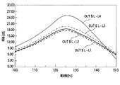
図2は、スイッチの開閉と増幅器の利得の変動との関係を示している。[S1S,S2S,S3S,S4S]=[S1D,S2D,S3D,S4D]=[On,On,On,On]の時の利得−周波数特性は、図2中のOUT$L_L4であり、[S1S,S2S,S3S,S4S]=[S1D,S2D,S3D,S4D]=[On,On,On,Off]の時の利得−周波数特性は、図2中のOUT$L_L3であり、[S1S,S2S,S3S,S4S]=[S1D,S2D,S3D,S4D]=[On,On,Off,Off]の時の利得−周波数特性は、図2中のOUT$L_L2であり、[S1S,S2S,S3S,S4S]=[S1D,S2D,S3D,S4D]=[On,Off,Off,Off]の時の利得−周波数特性は、図2中のOUT$L_L1である。この例ではインピーダンスの低下が利得の上昇という形で現れているが、これは回路定数の選び方によって、インピーダンスの低下が利得の低下を生ずる形にも設計できる。 FIG. 2 shows the relationship between opening and closing of the switch and fluctuations in the gain of the amplifier. The gain-frequency characteristic when [S1S, S2S, S3S, S4S] = [S1D, S2D, S3D, S4D] = [On, On, On, On] is OUT $ L_L4 in FIG. 2 and [S1S , S2S, S3S, S4S] = [S1D, S2D, S3D, S4D] = [On, On, On, Off], the gain-frequency characteristic is OUT $ L_L3 in FIG. 2 and [S1S, S2S , S3S, S4S] = [S1D, S2D, S3D, S4D] = [On, On, Off, Off], the gain-frequency characteristic is OUT $ L_L2 in FIG. 2, and [S1S, S2S, S3S] , S4S] = [S1D, S2D, S3D, S4D] = [On, Off, Off, Off], the gain-frequency characteristic is OUT $ L_L1 in FIG. In this example, a decrease in impedance appears in the form of an increase in gain, but this can also be designed in such a way that a decrease in impedance causes a decrease in gain depending on how the circuit constants are selected.
さらに、非特許文献3に記載のある通り、AC入力をVm×Cos(2πft)とした場合、
AC入力に対する歪率に対して最も影響を与える3次歪の大きさは、
AHD3/AF=Vm2/(32×(Vgs−Vth)2)
と表されるところ、本実施形態に係るインピーダンス制御はゲート・ソース間電圧Vgsを変化させないので、3次歪が変化せず歪率に対する影響が抑制されている。ここで、AHD3はトランジスタ出力3次歪振幅、AFはトランジスタ出力基本波振幅、Vgsはトランジスタのゲート−ソース間電圧、Vthはトランジスタの閾値電圧である。
Furthermore, as described in Non-Patent Document 3, when the AC input is Vm × Cos (2πft),
The magnitude of the third-order distortion that most affects the distortion rate for AC input is
AHD3 / AF = Vm 2 / (32 × (Vgs−Vth) 2 )
Since the impedance control according to this embodiment does not change the gate-source voltage Vgs, the third-order distortion does not change and the influence on the distortion rate is suppressed. Here, AHD3 is the transistor output third-order distortion amplitude, AF is the transistor output fundamental wave amplitude, Vgs is the gate-source voltage of the transistor, and Vth is the threshold voltage of the transistor.
なお、図1を参照して説明した本実施形態では、基準電位側インピーダンス制御回路と正電源電位側インピーダンス制御回路の両方が設けられているが、いずれかのみを設けた場合でも、インピーダンス制御が可能であり、同等の効果が得られることに留意されたい。換言すると、基準電位または正電源電位と増幅器とを接続する接続線のインピーダンスを制御するインピーダンス制御回路を少なくとも1つ設けることで、本実施形態の効果が得られる。 In the present embodiment described with reference to FIG. 1, both the reference potential side impedance control circuit and the positive power source potential side impedance control circuit are provided. However, even when only one of them is provided, the impedance control is not performed. Note that this is possible and the equivalent effect is obtained. In other words, the effect of the present embodiment can be obtained by providing at least one impedance control circuit for controlling the impedance of the connection line connecting the reference potential or the positive power supply potential and the amplifier.
ここで、図1には、増幅器として、M1、MC1,LL、LS、LIN、C1、RB、M2、AC入力入力端子IN、直流バイアス電流入力端子IB、出力端子OUTを構成要素として示してあるが、AC入力が入力されるトランジスタ(M1が対応)と、トランジスタのドレイン端子側に接続された負荷(LLが対応)と、基準電位(VSS1P8が対応)および正電源電位(VDD1P8が対応)とを備えていればよく、図1に示した形態に限定する意図はない。第3の実施形態に係る増幅器も参照されたい。なお、「ドレイン端子側に接続」とは、ドレイン端子に直接に接続される場合のみならず、MC1等の介在素子が存在する場合も包含することを意味する。 Here, in FIG. 1, as amplifiers, M1, MC1, LL, LS, LIN, C1, RB, M2, AC input input terminal IN, DC bias current input terminal IB, and output terminal OUT are shown as constituent elements. However, the transistor to which the AC input is input (corresponding to M1), the load connected to the drain terminal side of the transistor (corresponding to LL), the reference potential (corresponding to VSS1P8), and the positive power supply potential (corresponding to VDD1P8) And is not intended to be limited to the form shown in FIG. See also the amplifier according to the third embodiment. Note that “connected to the drain terminal side” means not only the case of being directly connected to the drain terminal but also the case where an intervening element such as MC1 is present.
(第2の実施形態)
図3は、第2の実施形態に係る増幅器を示している。増幅器300は、基準電位側インピーダンス制御素子および正電源電位側インピーダンス制御素子を除いて、第1の実施形態に係る増幅器100と同一である。増幅器300は、増幅器基準電位VSS1P8Iと増幅器正電源電位VDD1P8Iとの間に、可変容量CV1を備え、これをインピーダンス制御回路として用いる。インピーダンス変動の観点から見ると、直列のインダクタンス挿入と並列の容量挿入とは等価であり、第1の実施形態と同様のインピーダンス制御を行うことができる。
(Second Embodiment)
FIG. 3 shows an amplifier according to the second embodiment. The
なお、第2の実施形態を第1の実施形態と組み合わせて図4のように増幅器を構成することもできる。 Note that an amplifier can be configured as shown in FIG. 4 by combining the second embodiment with the first embodiment.
(第3の実施形態)
図5は、第3の実施形態に係る増幅器を示している。増幅器500は、ゲート接地の第1のトランジスタM1を備える。AC入力入力端子INが、直流阻止容量C1を介して第1のトランジスタM1のソース端子に接続されるとともに、インダクタLBに接続される。インダクタLBは、第1のトランジスタM1のソース−増幅器基準電位VSS1P8I間の直流パスを形成する。第1のトランジスタM1のドレイン端子が、カスコードトランジスタMC1のソース端子に接続される。
(Third embodiment)
FIG. 5 shows an amplifier according to the third embodiment. The
カスコードトランジスタMC1のゲート端子が、増幅器正電源電位VDD1P8Iに接続され、ドレイン端子は、負荷インダクタンスLLを介して増幅器正電源電位VDD1P8Iに接続される。増幅器300の出力は、カスコードトランジスタMC1のドレイン端子と負荷LLの接続点である出力端子OUTから取り出される。
The gate terminal of the cascode transistor MC1 is connected to the amplifier positive power supply potential VDD1P8I, and the drain terminal is connected to the amplifier positive power supply potential VDD1P8I via the load inductance LL. The output of the
第2のトランジスタM2のドレイン端子には、DC電流が加えられ、第2のトランジスタM2によって電流―電圧変換される。この電圧が第1のトランジスタM1へと導かれて第1のトランジスタM1直流動作点を決定する。 A DC current is applied to the drain terminal of the second transistor M2, and current-voltage conversion is performed by the second transistor M2. This voltage is guided to the first transistor M1 to determine the first transistor M1 DC operating point.
増幅器基準電位VSS1P8Iと基準電位VSS1P8との間のインピーダンスは、図1に示したように、インダクタンス素子L1S及びそれに直列に接続されるスイッチS1Sで構成される第1の基準電位側インピーダンス制御素子と、インダクタンスL2S及びスイッチS2Sで構成される第2の基準電位側インピーダンス制御素子と、インダクタンスL3S及びスイッチS3Sで構成される第3の基準電位側インピーダンス制御素子と、インダクタンスL4S及びスイッチS4Sで構成される第4の基準電位側インピーダンス制御素子とにより制御される。ここで、第2から第4の基準電位側インピーダンス制御素子は、第1の基準電位側インピーダンス制御素子と並列に接続されている。第1から第4の基準電位側インピーダンス制御素子を併せて、基準電位側インピーダンス制御回路と呼ぶ。 As shown in FIG. 1, the impedance between the amplifier reference potential VSS1P8I and the reference potential VSS1P8 includes an inductance element L1S and a first reference potential side impedance control element configured by a switch S1S connected in series thereto, A second reference potential side impedance control element composed of an inductance L2S and a switch S2S, a third reference potential side impedance control element composed of an inductance L3S and a switch S3S, and a second reference potential side impedance control element composed of an inductance L4S and a switch S4S. 4 is controlled by the reference potential side impedance control element. Here, the second to fourth reference potential side impedance control elements are connected in parallel with the first reference potential side impedance control element. The first to fourth reference potential side impedance control elements are collectively referred to as a reference potential side impedance control circuit.
また、増幅器正電源電位VDD1P8Iと正電源電位VDD1P8との間のインピーダンスは、インダクタンスL1D及びそれに直列接続されるスイッチS1Dで構成される第1の正電源電位側インピーダンス制御素子と、インダクタンスL2D及びスイッチS2Dで構成される第2の正電源電位側インピーダンス制御素子と、インダクタンスL3D及びスイッチS3Dで構成される第3の正電源電位側インピーダンス制御素子と、インダクタンスL4D及びスイッチS4Dで構成される第4の正電源電位側インピーダンス制御素子により制御される。ここで、第2から第4の正電源電位側インピーダンス制御素子は、第1の正電源電位側インピーダンス制御素子と並列に接続されている。第1から第4の正電源電位側インピーダンス制御素子を併せて、正電源電位側インピーダンス制御回路と呼ぶ。 In addition, the impedance between the amplifier positive power supply potential VDD1P8I and the positive power supply potential VDD1P8 is the first positive power supply potential side impedance control element including the inductance L1D and the switch S1D connected in series thereto, the inductance L2D, and the switch S2D. A second positive power supply potential side impedance control element constituted by the third positive power supply potential side impedance control element constituted by the inductance L3D and the switch S3D, and a fourth positive power supply constituted by the inductance L4D and the switch S4D. It is controlled by the power supply potential side impedance control element. Here, the second to fourth positive power supply potential side impedance control elements are connected in parallel with the first positive power supply potential side impedance control element. The first to fourth positive power supply potential side impedance control elements are collectively referred to as a positive power supply potential side impedance control circuit.
第3の実施形態に係る増幅器500は、第1の実施形態と同様に、第1〜第4の基準電位側インピーダンス制御素子または第1〜第4の正電源電位側インピーダンス制御素子のスイッチを開閉することによりインピーダンスを制御して、AC入力の歪率を変化させることなく利得を可変させることができる。
The
図6は、第2の実施形態と同様に、増幅器基準電位VSS1P8Iと増幅器正電源電位VDD1P8Iとの間に可変容量CV1を設けた増幅器を示している。図7は、第3の実施形態に係る増幅器と図6の増幅器とを組み合わせたものである。 FIG. 6 shows an amplifier in which a variable capacitor CV1 is provided between the amplifier reference potential VSS1P8I and the amplifier positive power supply potential VDD1P8I, as in the second embodiment. FIG. 7 is a combination of the amplifier according to the third embodiment and the amplifier of FIG.
100 増幅器
M1 トランジスタ
LL インダクタンス(負荷に対応)
VDD1P8 正電源電位
VSS1P8 基準電位
IN AC入力入力端子
OUT 出力端子
100 amplifier M1 transistor LL inductance (corresponding to load)
VDD1P8 Positive power supply potential VSS1P8 Reference potential IN AC input input terminal OUT output terminal
Claims (4)
基準電位と前記トランジスタのソース端子側とを接続する第1の接続線、および正電源電位と前記トランジスタのドレイン端子側とを接続する第2の接続線のうちの少なくとも一方のインピーダンスを制御するインピーダンス制御回路
を備えることを特徴とする増幅器。 An amplifier comprising a transistor to which an AC input is input and a load connected to the drain terminal side of the transistor,
Impedance that controls the impedance of at least one of a first connection line that connects a reference potential and the source terminal side of the transistor, and a second connection line that connects a positive power supply potential and the drain terminal side of the transistor An amplifier comprising a control circuit.
インダクタンス素子および前記インダクタンス素子に直列に接続されるスイッチで構成されるインピーダンス制御素子が複数並列に接続されており、
前記基準電位と前記トランジスタのソース端子との間、または前記正電源電位と前記トランジスタのドレイン端子との間の少なくとも一方に配置されている
ことを特徴とする請求項1に記載の増幅器。 The impedance control circuit includes:
A plurality of impedance control elements composed of an inductance element and a switch connected in series to the inductance element are connected in parallel,
2. The amplifier according to claim 1, wherein the amplifier is disposed between at least one of the reference potential and the source terminal of the transistor or between the positive power supply potential and the drain terminal of the transistor.
前記第1の接続線と前記第2の接続線との間に配置された可変容量であることを特徴とする請求項1に記載の増幅器。 The impedance control circuit includes:
The amplifier according to claim 1, wherein the amplifier is a variable capacitor disposed between the first connection line and the second connection line.
Priority Applications (1)
| Application Number | Priority Date | Filing Date | Title |
|---|---|---|---|
| JP2008041992A JP2009200958A (en) | 2008-02-22 | 2008-02-22 | Amplifier |
Applications Claiming Priority (1)
| Application Number | Priority Date | Filing Date | Title |
|---|---|---|---|
| JP2008041992A JP2009200958A (en) | 2008-02-22 | 2008-02-22 | Amplifier |
Publications (1)
| Publication Number | Publication Date |
|---|---|
| JP2009200958A true JP2009200958A (en) | 2009-09-03 |
Family
ID=41143958
Family Applications (1)
| Application Number | Title | Priority Date | Filing Date |
|---|---|---|---|
| JP2008041992A Pending JP2009200958A (en) | 2008-02-22 | 2008-02-22 | Amplifier |
Country Status (1)
| Country | Link |
|---|---|
| JP (1) | JP2009200958A (en) |
Cited By (3)
| Publication number | Priority date | Publication date | Assignee | Title |
|---|---|---|---|---|
| JP2012239126A (en) * | 2011-05-13 | 2012-12-06 | Asahi Kasei Electronics Co Ltd | Amplifier |
| JP2014209672A (en) * | 2013-04-16 | 2014-11-06 | 三菱電機株式会社 | Power amplifier |
| JP2016508702A (en) * | 2013-02-22 | 2016-03-22 | クゥアルコム・インコーポレイテッドQualcomm Incorporated | Amplifier with multiple outputs and configurable degeneration inductors |
Citations (2)
| Publication number | Priority date | Publication date | Assignee | Title |
|---|---|---|---|---|
| JP2002094345A (en) * | 2000-08-24 | 2002-03-29 | Internatl Business Mach Corp <Ibm> | Variable gain amplifier |
| JP2004282506A (en) * | 2003-03-17 | 2004-10-07 | Matsushita Electric Ind Co Ltd | Variable gain amplifier circuit |
-
2008
- 2008-02-22 JP JP2008041992A patent/JP2009200958A/en active Pending
Patent Citations (2)
| Publication number | Priority date | Publication date | Assignee | Title |
|---|---|---|---|---|
| JP2002094345A (en) * | 2000-08-24 | 2002-03-29 | Internatl Business Mach Corp <Ibm> | Variable gain amplifier |
| JP2004282506A (en) * | 2003-03-17 | 2004-10-07 | Matsushita Electric Ind Co Ltd | Variable gain amplifier circuit |
Cited By (3)
| Publication number | Priority date | Publication date | Assignee | Title |
|---|---|---|---|---|
| JP2012239126A (en) * | 2011-05-13 | 2012-12-06 | Asahi Kasei Electronics Co Ltd | Amplifier |
| JP2016508702A (en) * | 2013-02-22 | 2016-03-22 | クゥアルコム・インコーポレイテッドQualcomm Incorporated | Amplifier with multiple outputs and configurable degeneration inductors |
| JP2014209672A (en) * | 2013-04-16 | 2014-11-06 | 三菱電機株式会社 | Power amplifier |
Similar Documents
| Publication | Publication Date | Title |
|---|---|---|
| US8648660B2 (en) | Amplifier with non-linear current mirror | |
| JP5720106B2 (en) | Mixer circuit and method for adjusting common voltage of mixer circuit | |
| US9503022B2 (en) | Balanced up-conversion mixer | |
| JP4773258B2 (en) | Power amplifier with automatic switching function | |
| JP2007174029A (en) | Gain variable circuit and automatic gain control amplifier using the same | |
| US20100001797A1 (en) | Differential amplifier | |
| US7795975B2 (en) | Class AB amplifier | |
| JP2009200958A (en) | Amplifier | |
| US9054651B2 (en) | Power amplifier circuit | |
| US7528658B2 (en) | Threshold voltage compensation for a two stage amplifier | |
| JP4907395B2 (en) | Variable gain amplifier circuit | |
| JP4991915B2 (en) | Frequency conversion circuit, signal processing circuit, and receiver | |
| JP2007116569A (en) | Open gain adjustment circuit for operational amplifier | |
| JP2009089225A (en) | Variable gain amplifying device | |
| JP5385335B2 (en) | amplifier | |
| US8665015B1 (en) | Power amplifier circuit | |
| JP4331550B2 (en) | Phase compensation circuit | |
| US7009442B2 (en) | Linear multiplier circuit | |
| TWI436586B (en) | Variable gain amplifier and receiver device | |
| CN104953968A (en) | Semiconductor circuit and amplifier circuit | |
| JP5204902B2 (en) | Transfer gate circuit and power combiner circuit, power amplifier circuit, transmitter and communication device using the same | |
| JP2010056606A (en) | Transconductance amplifier | |
| JP5308407B2 (en) | Amplifier circuit | |
| US10868505B1 (en) | CMOS input stage circuits and related methods | |
| Noormohammadi et al. | A new class AB multipath telescopic-cascode operational amplifier |
Legal Events
| Date | Code | Title | Description |
|---|---|---|---|
| A621 | Written request for application examination |
Effective date: 20090813 Free format text: JAPANESE INTERMEDIATE CODE: A621 |
|
| A977 | Report on retrieval |
Free format text: JAPANESE INTERMEDIATE CODE: A971007 Effective date: 20110324 |
|
| A131 | Notification of reasons for refusal |
Effective date: 20110329 Free format text: JAPANESE INTERMEDIATE CODE: A131 |
|
| A02 | Decision of refusal |
Effective date: 20110809 Free format text: JAPANESE INTERMEDIATE CODE: A02 |