JP2014204603A - Power feeding apparatus and power feeding system - Google Patents
Power feeding apparatus and power feeding system Download PDFInfo
- Publication number
- JP2014204603A JP2014204603A JP2013080429A JP2013080429A JP2014204603A JP 2014204603 A JP2014204603 A JP 2014204603A JP 2013080429 A JP2013080429 A JP 2013080429A JP 2013080429 A JP2013080429 A JP 2013080429A JP 2014204603 A JP2014204603 A JP 2014204603A
- Authority
- JP
- Japan
- Prior art keywords
- coupling coefficient
- power
- power supply
- power transmission
- frequency
- Prior art date
- Legal status (The legal status is an assumption and is not a legal conclusion. Google has not performed a legal analysis and makes no representation as to the accuracy of the status listed.)
- Pending
Links
- 230000008878 coupling Effects 0.000 claims abstract description 215
- 238000010168 coupling process Methods 0.000 claims abstract description 215
- 238000005859 coupling reaction Methods 0.000 claims abstract description 215
- 230000005540 biological transmission Effects 0.000 claims abstract description 160
- 238000004364 calculation method Methods 0.000 claims abstract description 114
- 238000005259 measurement Methods 0.000 claims abstract description 78
- 230000007274 generation of a signal involved in cell-cell signaling Effects 0.000 claims description 31
- 238000001514 detection method Methods 0.000 claims description 25
- 230000004913 activation Effects 0.000 claims description 11
- 230000003071 parasitic effect Effects 0.000 claims description 5
- 239000003990 capacitor Substances 0.000 description 65
- 238000000034 method Methods 0.000 description 41
- 238000004891 communication Methods 0.000 description 28
- 230000006870 function Effects 0.000 description 26
- 238000010586 diagram Methods 0.000 description 17
- 230000004048 modification Effects 0.000 description 11
- 238000012986 modification Methods 0.000 description 11
- 230000005674 electromagnetic induction Effects 0.000 description 6
- 230000004907 flux Effects 0.000 description 6
- 230000020169 heat generation Effects 0.000 description 6
- 230000008859 change Effects 0.000 description 5
- 230000000052 comparative effect Effects 0.000 description 5
- 230000005855 radiation Effects 0.000 description 5
- 230000008901 benefit Effects 0.000 description 3
- 230000000694 effects Effects 0.000 description 3
- 229910052751 metal Inorganic materials 0.000 description 3
- 239000002184 metal Substances 0.000 description 3
- 230000008569 process Effects 0.000 description 3
- 238000009774 resonance method Methods 0.000 description 3
- 238000005516 engineering process Methods 0.000 description 2
- 238000007429 general method Methods 0.000 description 2
- 238000005457 optimization Methods 0.000 description 2
- 230000009467 reduction Effects 0.000 description 2
- 230000007704 transition Effects 0.000 description 2
- 238000004804 winding Methods 0.000 description 2
- HBBGRARXTFLTSG-UHFFFAOYSA-N Lithium ion Chemical compound [Li+] HBBGRARXTFLTSG-UHFFFAOYSA-N 0.000 description 1
- 206010037660 Pyrexia Diseases 0.000 description 1
- 230000001413 cellular effect Effects 0.000 description 1
- 238000006243 chemical reaction Methods 0.000 description 1
- 238000009499 grossing Methods 0.000 description 1
- 230000006698 induction Effects 0.000 description 1
- 229910001416 lithium ion Inorganic materials 0.000 description 1
- 239000000696 magnetic material Substances 0.000 description 1
- 238000000691 measurement method Methods 0.000 description 1
- 229910044991 metal oxide Inorganic materials 0.000 description 1
- 150000004706 metal oxides Chemical class 0.000 description 1
- 150000002739 metals Chemical class 0.000 description 1
- 238000010248 power generation Methods 0.000 description 1
- 239000004065 semiconductor Substances 0.000 description 1
- 238000010408 sweeping Methods 0.000 description 1
- 230000001360 synchronised effect Effects 0.000 description 1
Images


Classifications
-
- H—ELECTRICITY
- H02—GENERATION; CONVERSION OR DISTRIBUTION OF ELECTRIC POWER
- H02J—CIRCUIT ARRANGEMENTS OR SYSTEMS FOR SUPPLYING OR DISTRIBUTING ELECTRIC POWER; SYSTEMS FOR STORING ELECTRIC ENERGY
- H02J50/00—Circuit arrangements or systems for wireless supply or distribution of electric power
- H02J50/90—Circuit arrangements or systems for wireless supply or distribution of electric power involving detection or optimisation of position, e.g. alignment
-
- H—ELECTRICITY
- H02—GENERATION; CONVERSION OR DISTRIBUTION OF ELECTRIC POWER
- H02J—CIRCUIT ARRANGEMENTS OR SYSTEMS FOR SUPPLYING OR DISTRIBUTING ELECTRIC POWER; SYSTEMS FOR STORING ELECTRIC ENERGY
- H02J50/00—Circuit arrangements or systems for wireless supply or distribution of electric power
- H02J50/10—Circuit arrangements or systems for wireless supply or distribution of electric power using inductive coupling
- H02J50/12—Circuit arrangements or systems for wireless supply or distribution of electric power using inductive coupling of the resonant type
-
- H—ELECTRICITY
- H02—GENERATION; CONVERSION OR DISTRIBUTION OF ELECTRIC POWER
- H02J—CIRCUIT ARRANGEMENTS OR SYSTEMS FOR SUPPLYING OR DISTRIBUTING ELECTRIC POWER; SYSTEMS FOR STORING ELECTRIC ENERGY
- H02J50/00—Circuit arrangements or systems for wireless supply or distribution of electric power
- H02J50/40—Circuit arrangements or systems for wireless supply or distribution of electric power using two or more transmitting or receiving devices
-
- H—ELECTRICITY
- H02—GENERATION; CONVERSION OR DISTRIBUTION OF ELECTRIC POWER
- H02J—CIRCUIT ARRANGEMENTS OR SYSTEMS FOR SUPPLYING OR DISTRIBUTING ELECTRIC POWER; SYSTEMS FOR STORING ELECTRIC ENERGY
- H02J50/00—Circuit arrangements or systems for wireless supply or distribution of electric power
- H02J50/60—Circuit arrangements or systems for wireless supply or distribution of electric power responsive to the presence of foreign objects, e.g. detection of living beings
-
- H04B5/79—
-
- H—ELECTRICITY
- H02—GENERATION; CONVERSION OR DISTRIBUTION OF ELECTRIC POWER
- H02J—CIRCUIT ARRANGEMENTS OR SYSTEMS FOR SUPPLYING OR DISTRIBUTING ELECTRIC POWER; SYSTEMS FOR STORING ELECTRIC ENERGY
- H02J7/00—Circuit arrangements for charging or depolarising batteries or for supplying loads from batteries
- H02J7/00032—Circuit arrangements for charging or depolarising batteries or for supplying loads from batteries characterised by data exchange
- H02J7/00034—Charger exchanging data with an electronic device, i.e. telephone, whose internal battery is under charge
Abstract
Description
本開示は、電子機器等の給電対象機器に対して非接触に電力供給(送電,電力伝送)を行う給電システム、ならびにそのような給電システムに適用される給電装置に関する。 The present disclosure relates to a power supply system that performs non-contact power supply (power transmission, power transmission) to a power supply target device such as an electronic device, and a power supply device applied to such a power supply system.
近年、例えば携帯電話機や携帯音楽プレーヤー等のCE機器(Consumer Electronics Device:民生用電子機器)に対し、非接触に電力供給を行う給電システム(非接触給電システム、ワイヤレス充電システム)が注目を集めている。これにより、ACアダプタのような電源装置のコネクタを機器に挿す(接続する)ことによって充電を開始するのはなく、電子機器(2次側機器)を充電トレー(1次側機器)上に置くだけで充電を開始することができる。すなわち、電子機器と充電トレーと間での端子接続が不要となる。 In recent years, power supply systems (contactless power supply systems, wireless charging systems) that supply power in a non-contact manner to CE devices (consumer electronics devices) such as mobile phones and portable music players have attracted attention in recent years. Yes. Thus, charging is not started by inserting (connecting) a connector of a power supply device such as an AC adapter into the device, and the electronic device (secondary device) is placed on the charging tray (primary device). Just start charging. That is, terminal connection between the electronic device and the charging tray becomes unnecessary.
このようにして非接触で電力供給を行う方式としては、電磁誘導方式が良く知られている。また、最近では、電磁共鳴現象を利用した磁界共鳴方式と呼ばれる方式を用いた非接触給電システムが注目されている。このような非接触による給電システムは、例えば特許文献1〜2等に開示されている。
An electromagnetic induction method is well known as a method for supplying power without contact in this manner. Recently, a non-contact power feeding system using a method called a magnetic field resonance method using an electromagnetic resonance phenomenon has attracted attention. Such a non-contact power feeding system is disclosed in, for example,
ところで、上記のような非接触による給電システムでは、1次側機器(送電コイル)と2次側機器(受電コイル)との間の結合係数を簡易に得ることが求められている。したがって、そのような結合係数を簡易に求めることを可能とする手法の提案が望まれる。 By the way, in the non-contact power supply system as described above, it is required to easily obtain a coupling coefficient between the primary side device (power transmission coil) and the secondary side device (power reception coil). Therefore, it is desired to propose a method that makes it possible to easily obtain such a coupling coefficient.
本開示はかかる問題点に鑑みてなされたもので、その目的は、磁界を用いて電力伝送を行う際の結合係数を簡易に求めることが可能な給電装置および給電システムを提供することにある。 The present disclosure has been made in view of such problems, and an object of the present disclosure is to provide a power feeding device and a power feeding system capable of easily obtaining a coupling coefficient when performing power transmission using a magnetic field.
本開示の給電装置は、磁界を用いた送電を行うための送電コイルと、この送電コイルと給電対象機器内の受電コイルとの間の結合係数を算出する結合係数算出部とを備えたものである。結合係数算出部は、給電対象機器内の整流回路の非動作状態時における入力インピーダンスの周波数特性を測定し、その周波数特性の測定結果を利用して結合係数を算出する。 A power supply apparatus according to the present disclosure includes a power transmission coil for performing power transmission using a magnetic field, and a coupling coefficient calculation unit that calculates a coupling coefficient between the power transmission coil and a power reception coil in a power supply target device. is there. The coupling coefficient calculation unit measures the frequency characteristics of the input impedance when the rectifier circuit in the power supply target device is not operating, and calculates the coupling coefficient using the measurement result of the frequency characteristics.
本開示の給電システムは、受電コイルおよび整流回路を有する1または複数の電子機器(給電対象機器)と、この電子機器に対して磁界を用いた送電を行う上記本開示の給電装置とを備えたものである。 A power feeding system according to the present disclosure includes one or a plurality of electronic devices (power feeding target devices) each having a power receiving coil and a rectifier circuit, and the power feeding device according to the present disclosure that performs power transmission using a magnetic field to the electronic devices. Is.
本開示の給電装置および給電システムでは、給電対象機器(電子機器)内の整流回路の非動作状態時における入力インピーダンスの周波数特性が測定され、その周波数特性の測定結果を利用して、送電コイルと受電コイルとの間の結合係数が算出される。これにより、例えば給電対象機器に対して動的な制御を行うような複雑な手法を用いずに、結合係数を得ることができる。 In the power supply device and the power supply system of the present disclosure, the frequency characteristic of the input impedance when the rectifier circuit in the power supply target device (electronic device) is not operating is measured, and the measurement result of the frequency characteristic is used to A coupling coefficient with the power receiving coil is calculated. Thereby, for example, a coupling coefficient can be obtained without using a complicated method for performing dynamic control on a power supply target device.
本開示の給電装置および給電システムによれば、整流回路の非動作状態時における入力インピーダンスの周波数特性の測定結果を利用して結合係数を算出するようにしたので、複雑な手法を用いずに結合係数を得ることができる。よって、磁界を用いて電力伝送を行う際の結合係数を簡易に求めることが可能となる。 According to the power supply device and the power supply system of the present disclosure, since the coupling coefficient is calculated using the measurement result of the frequency characteristic of the input impedance when the rectifier circuit is not in operation, the coupling can be performed without using a complicated method. A coefficient can be obtained. Therefore, it is possible to easily obtain a coupling coefficient when performing power transmission using a magnetic field.
以下、本開示の実施の形態について、図面を参照して詳細に説明する。なお、説明は以下の順序で行う。
1.第1の実施の形態(極小値時および極大値時の周波数を用いて結合係数を求める例)
2.第2の実施の形態(2つの極小値時の周波数を用いて結合係数を求める例)
3.変形例1,2(2次側機器内におけるバイパス経路の他の配置構成例)
4.第3の実施の形態(求められた結合係数を利用して給電パラメータを設定する例)
5.第4の実施の形態(結合係数を求める際に併せて給電対象機器の有無を検知する例)
6.第5の実施の形態(求められた結合係数の大きさに応じて送電制御を行う例)
7.その他の変形例
Hereinafter, embodiments of the present disclosure will be described in detail with reference to the drawings. The description will be given in the following order.
1. First Embodiment (Example of obtaining a coupling coefficient using the frequency at the minimum value and the maximum value)
2. Second embodiment (an example in which a coupling coefficient is obtained by using frequencies at two local minimum values)
3.
4). Third embodiment (example in which power supply parameters are set using the obtained coupling coefficient)
5. Fourth embodiment (an example in which presence / absence of a power supply target device is detected when obtaining a coupling coefficient)
6). Fifth embodiment (an example in which power transmission control is performed according to the obtained coupling coefficient)
7). Other variations
<第1の実施の形態>
[給電システム4の全体構成]
図1は、本開示の第1の実施の形態に係る給電システム(給電システム4)の外観構成例を表したものであり、図2は、この給電システム4のブロック構成例を表したものである。給電システム4は、磁界を用いて(磁界共鳴や電磁誘導等を利用して;以下同様)、非接触に電力伝送(電力供給,給電,送電)を行うシステム(非接触型の給電システム)である。この給電システム4は、給電装置1(1次側機器)と、給電対象機器としての1または複数の電子機器(ここでは2つの電子機器2A,2B;2次側機器)とを備えている。
<First Embodiment>
[Overall configuration of power supply system 4]
FIG. 1 illustrates an external configuration example of the power feeding system (power feeding system 4) according to the first embodiment of the present disclosure, and FIG. 2 illustrates a block configuration example of the power feeding system 4. is there. The power feeding system 4 is a system (non-contact type power feeding system) that performs power transmission (power supply, power feeding, power transmission) in a non-contact manner using a magnetic field (using magnetic field resonance, electromagnetic induction, etc .; the same applies hereinafter). is there. The power supply system 4 includes a power supply device 1 (primary device) and one or a plurality of electronic devices (here, two
この給電システム4では、例えば図1に示したように、給電装置1における給電面(送電面)S1上に電子機器2A,2Bが置かれる(または近接する)ことにより、給電装置1から電子機器2A,2Bに対して送電が行われるようになっている。ここでは、複数の電子機器2A,2Bに対して同時もしくは時分割的(順次)に送電を行う場合を考慮して、給電装置1は、給電面S1の面積が給電対象の電子機器2A,2B等よりも大きなマット形状(トレー状)となっている。
In the power supply system 4, for example, as shown in FIG. 1, the
(給電装置1)
給電装置1は、上記したように、磁界を用いて電子機器2A,2Bに対して送電を行うもの(充電トレー)である。この給電装置1は、例えば図2に示したように、送電部110、交流信号発生回路(交流信号発生部,高周波電力発生回路)111、結合係数算出回路112(結合係数算出部)、通信部113および制御部114を有する送電装置11を備えている。また、この送電装置11内には、図示しないスイッチ(後述するスイッチング素子SW2)が設けられている。
(Power supply device 1)
As described above, the
送電部110は、後述する送電コイル(1次側コイル)L1およびコンデンサC1(共振用のコンデンサ)等を含んで構成されており、後述するように、これらの送電コイルL1およびコンデンサC1を用いてLC共振回路が構成されている。送電部110は、これらの送電コイルL1およびコンデンサC1を利用して、電子機器2A,2B(詳細には、後述する受電部210)に対して交流磁界を用いた送電を行うものである(図2中の矢印P1参照)。具体的には、送電部110は、給電面S1から電子機器2A,2Bへ向けて磁界(磁束)を放射する機能を有している。
The
交流信号発生回路111は、例えば給電装置1の外部電源9(親電源)から供給される電力を用いて、送電を行うための所定の交流信号Sac(高周波電力)を発生する回路である。この交流信号Sacは、送電部110へ向けて供給されるようになっている。このような交流信号発生回路111は、例えば、後述するスイッチング素子SW1を含んだスイッチングアンプを用いて構成されている。なお、外部電源9としては、例えば、通常のACアダプタや、PC(Personal Computer)などに設けられているUSB(Universal Serial Bus)2.0の電源(電力供給能力:500mA,電源電圧:5V程度)等が挙げられる。
The AC
結合係数算出回路112は、後述する送電コイルL1と電子機器2A,2B内の後述する受電コイルL2との間の結合係数kを算出する回路である。この結合係数kとは、送電コイルL1と受電コイルL2との間における磁束の共有度を表すパラメータである。なお、この結合係数算出回路112による結合係数kの算出方法の詳細については、後述する。
The coupling
通信部113は、電子機器2A,2B内の後述する通信部214との間で、所定の通信動作を相互に行うものである(図2中の矢印C1参照)。
The
制御部114は、給電装置1全体(給電システム4全体)における種々の制御動作を行うものである。具体的には、送電部110による送電動作や通信部113による通信動作の制御を行うことの他、例えば、送電電力の最適化制御や給電対象機器を認証する機能、給電対象機器が近傍にあることを検知する機能、異種金属等の混入を検知する機能などを有している。また、本実施の形態では、制御部114は、結合係数算出回路112による結合係数の算出動作を制御する機能も有している。ここで、上記した送電動作の制御の際には、後述する所定の制御信号CTL(送電用の制御信号)を用いて交流信号発生回路111の動作を制御することによって行うようになっている。このような制御部114は、例えば、マイクロコンピュータやパルスジェネレータ等を用いて構成されている。
The
(電子機器2A,2B)
電子機器2A,2Bは、例えば、テレビ受像機に代表される据え置き型電子機器や、携帯電話やデジタルカメラに代表される、充電池(バッテリー)を含む携帯型の電子機器等からなる。これらの電子機器2A,2Bは、例えば図2に示したように、受電装置21と、この受電装置21から供給される電力に基づいて所定の動作(電子機器としての機能を発揮させる動作)を行う負荷22とを備えている。また、受電装置21は、受電部210、整流回路211、給電・充電制御回路212、バッテリー213、通信部214、制御部215およびコンデンサC2pを有している。なお、このコンデンサC2pが、本開示における「容量素子」の一具体例に対応している。
(
The
受電部210は、後述する受電コイル(2次側コイル)L2およびコンデンサC2(共振用のコンデンサ)等を含んで構成されている。そして、後述するように、これらの受電コイルL2およびコンデンサC2と、上記したコンデンサC2pとを用いて、LC共振回路が構成されている。受電部210は、これらの受電コイルL2およびコンデンサC2等を利用して、給電装置1内の送電部110から伝送された電力(送電電力)を受け取る機能を有している。
The
整流回路211は、受電部210から供給された送電電力(交流電力)を整流し、直流電力を生成する回路である。
The
給電・充電制御回路212は、整流回路211から出力される直流電力に基づいて、バッテリー213への充電制御を行うと共に、負荷22への給電制御を行う回路である。
The power supply /
バッテリー213は、給電・充電制御回路212による充電制御に従って電力を貯蔵するものであり、例えばリチウムイオン電池等の充電池(2次電池)を用いて構成されている。
The
通信部214は、給電装置1内の通信部113との間で、前述した所定の通信動作を相互に行うものである(図2中の矢印C1参照)。
The
制御部215は、電子機器2Aまたは電子機器2Bの全体(給電システム4全体)における種々の制御動作を行うものである。具体的には、受電部210による受電動作や通信部214による通信動作の制御を行うことの他、例えば、受電電力の最適化制御を行ったり、給電・充電制御回路212の動作を制御したりする機能等を有している。このような制御部215は、例えば、マイクロコンピュータ等を用いて構成されている。
The
[給電装置1および電子機器2A,2Bの詳細構成]
図3は、図2に示した給電装置1および電子機器2A,2B内の各ブロックの詳細構成例を回路図およびブロック図で表したものである。
[Detailed Configuration of
FIG. 3 is a circuit diagram and a block diagram illustrating a detailed configuration example of each block in the
(送電部110)
送電部110は、磁界を用いて送電を行う(磁束を発生させる)ための送電コイルL1と、この送電コイルL1とともに前述したLC共振回路を形成するためのコンデンサC1とを有している。これらの送電コイルL1とコンデンサC1とは、互いに電気的に直列接続されている。具体的には、送電コイルL1の一端はコンデンサC1の一端に接続され、送電コイルL1の他端は接地され、コンデンサC1の他端は電力供給ラインLpを介して交流信号発生回路111の出力端子に接続されている。
(Power transmission unit 110)
The
また、この送電部110内に形成されるLC共振回路と、後述する受電部210内等に形成されるLC共振回路とは、互いに磁気結合する(相互誘導)。これにより、交流信号発生回路111により生成された高周波電力(交流信号Sac)と略同一の共振周波数によるLC共振動作がなされるようになっている。
In addition, an LC resonance circuit formed in the
(交流信号発生回路111)
交流信号発生回路111は、MOS(Metal Oxide Semiconductor)トランジスタ等からなる1または複数のスイッチング素子SW1を含んだ、スイッチングアンプ(図示せず;いわゆるD級アンプやE級アンプ等)を用いて構成されている。この交流信号発生回路111には、制御部114から送電用の制御信号CTLが供給されるようになっている。この制御信号CTLは、所定の周波数f(CTL(f)=f1)およびデューティ比Duty(CTL(Duty)=10%,50%等)を示すパルス信号からなる。
(AC signal generation circuit 111)
The AC
このような構成により交流信号発生回路111では、送電用の制御信号CTLに従って、上記したスイッチング素子SW1がオン・オフ動作(上記した周波数fおよびデューティ比Dutyからなるスイッチング動作)を行う。すなわち、制御部114から供給される制御信号CTLを用いて、スイッチング素子SW1のオン・オフ動作が制御される。これにより、例えば外部電源9側から入力する直流信号Sdcに基づいて交流信号Sacが生成され、送電部110へ供給されるようになっている。
With such a configuration, in the AC
(結合係数算出回路112)
結合係数算出回路112は、電力供給ラインLpに対してスイッチング素子SW2を介して接続可能に配置されており、前述したように、送電コイルL1と受電コイルL2との間の結合係数を算出する機能を有している。なお、このスイッチング素子SW2は、制御部114による制御に従って、結合係数の算出時にオン状態となるように設定されている。
(Coupling coefficient calculation circuit 112)
The coupling
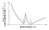
この結合係数算出回路112は、電子機器2A,2B内の整流回路211の非動作状態時における、給電装置1側からみた入力インピーダンスZinの周波数特性を測定し、その周波数特性の測定結果を利用して結合係数kを算出する。具体的には、この周波数特性の測定結果から、入力インピーダンスZinの極値時の周波数fを検出し、その極値時の周波数fを用いて結合係数を算出する。
The coupling
特に本実施の形態では、詳細は後述するが、結合係数算出回路112は、この極値時の周波数fとして、極小値時の周波数(後述する周波数fH)と極大値時の周波数(後述する周波数fL)との双方を検出し、それら双方の周波数fH,fLを用いて結合係数kを算出するようになっている。また、本実施の形態では、結合係数算出回路112は、微弱信号(測定電力が微弱である測定信号)を用いて入力インピーダンスZinの周波数特性を測定することにより、上記したような整流回路211の非動作状態時における周波数特性の測定を行うようになっている。
In particular, in this embodiment, although the details will be described later, the coupling
結合係数算出回路112は、図3に示したように、測定信号発生部30、電流検出回路31(電流検出部)、アンプ32、A/D変換器33および算出・制御部34を有している。なお、この算出・制御部34が、本開示における「算出部」および「制御部」の一具体例に対応する。
As shown in FIG. 3, the coupling
測定信号発生部30は、入力インピーダンスZinの周波数特性を測定するための測定信号を発生させるものであり、この例では交流電源を用いて構成されている。この測定信号は、所定の電圧Vおよび周波数fを有する信号であり、スイッチング素子SW2を介して電力供給ラインLpから送電部110へ供給されるようになっている。
The
電流検出回路31は、入力インピーダンスZinの周波数特性を測定する際に送電コイルL1に流れる電流I(測定電流)を検出する回路である。このようにして検出された電流Iの値(この例ではアナログ値)は、アンプ32へ供給されるようになっている。このような電流検出回路31は、例えば、抵抗器やカレントトランス等を用いて構成されている。
The
アンプ32は、電流検出回路31により検出された電流Iの値(信号)を増幅する機能を有する回路(増幅回路)である。
The
A/D変換器33は、アンプ32から出力されたアナログ値の電流Iに対してA/D(アナログ/デジタル)変換を行い、デジタル値からなる電流Iを出力するものである。
The A /
算出・制御部34は、まず、測定信号発生部30の動作を制御することにより、測定信号の電圧Vおよび周波数fをそれぞれ制御する機能を有している。また、算出・制御部34は、電流検出回路31により検出された電流Iと、自身により設定された測定信号の電圧Vとに基づいて、入力インピーダンスZinを算出する(Zin=V/I)機能を有している。この際、測定信号の周波数fを連続的に変化させていく(周波数fの値を掃引する)ことにより、入力インピーダンスZinの周波数特性が得られるようになっている。なお、この算出・制御部34による制御機能および算出機能の詳細については、後述する。
First, the calculation /
(受電部210,バイパス経路Lb)
受電部210は、送電部110から伝送された(交流磁界から)電力を受け取るための受電コイルL2と、この受電コイルL2とともに前述したLC共振回路を形成するためのコンデンサC2とを有している。これらの受電コイルL2とコンデンサC2とは互いに電気的に直列接続されており、前述したコンデンサC2pはこの受電部210に対して電気的に並列接続されている。具体的には、コンデンサC2の一端は、整流回路211における一方の入力端子およびコンデンサC2pの一端に接続され、コンデンサC2の他端は受電コイルL2の一端に接続されている。また、受電コイルL2の他端は、整流回路211における他方の入力端子およびコンデンサC2pの他端に接続されている。
(
The
ここで、受電コイルL2とコンデンサC2,C2pとからなるLC共振回路と、前述した送電コイルL1とコンデンサC1とからなるLC共振回路とは、互いに磁気結合する。これにより、交流信号発生回路111により生成された高周波電力(交流信号Sac)と略同一の共振周波数によるLC共振動作がなされるようになっている。
Here, the LC resonance circuit including the power receiving coil L2 and the capacitors C2 and C2p and the LC resonance circuit including the power transmission coil L1 and the capacitor C1 are magnetically coupled to each other. As a result, LC resonance operation is performed at substantially the same resonance frequency as the high-frequency power (AC signal Sac) generated by the AC
また、図3に示したように、コンデンサC2pが配置された経路(バイパス経路Lb)は、受電部210に対して電気的に並列接続されると共に、整流回路211における一対の入力端子間に配置されている。このバイパス経路Lbは、整流回路211に対するバイパス経路として機能するものである。これにより詳細は後述するが、入力インピーダンスZinの周波数特性の測定時に、整流回路211が非動作状態(無効状態,不活性状態)となるようになっている。
Further, as shown in FIG. 3, the path (bypass path Lb) in which the capacitor C2p is arranged is electrically connected in parallel to the
(整流回路211)
整流回路211は、ここでは4つの整流素子(ダイオード)D1〜D4および平滑用のコンデンサC3を用いて構成されている。この図3の例では、整流素子D1のアノードおよび整流素子D3のカソードは、互いに整流回路211における一方の入力端子に接続され、整流素子D1のカソードおよび整流素子D2のカソードは、互いに整流回路211における出力端子に接続されている。また、整流素子D2のアノードおよび整流素子D4のカソードは、互いに整流回路211における他方の入力端子に接続され、整流素子D3のアノードおよび整流素子D4のアノードは、互いに接地されている。すなわち、この整流回路211は、いわゆるダイオードブリッジ構成の回路となっている。また、コンデンサC3は、整流素子D1,D2のカソード同士の接続点と給電・充電制御回路212との間の経路と接地との間に配置されている。このような構成により整流回路211では、受電部210から供給された交流電力を整流すると共に、その整流後電力を平滑して脈流を低減し、直流電力からなる受電電力を給電・充電制御回路212へ供給するようになっている。なお、この整流回路211が、トランジスタを用いた同期整流回路であってもよい。
(Rectifier circuit 211)
Here, the rectifying
[給電システム4の作用・効果]
(全体動作の概要)
この給電システム4では、給電装置1内の交流信号発生回路111が、外部電源9から供給される電力に基づいて、送電部110内の送電コイルL1およびコンデンサC1に対して、送電を行うための所定の高周波電力(交流信号Sac)を供給する。これにより、送電部110内の送電コイルL1において磁界(磁束)が発生する。このとき、給電装置1の上面(給電面S1)に、給電対象機器としての電子機器2A,2Bが置かれる(または近接する)と、給電装置1内の送電コイルL1と電子機器2A,2B内の受電コイルL2とが、給電面S1付近にて近接する。
[Operation and effect of power feeding system 4]
(Overview of overall operation)
In the power supply system 4, the AC
このように、磁界を発生している送電コイルL1に近接して受電コイルL2が配置されると、送電コイルL1から発生されている磁束に誘起されて、受電コイルL2に起電力(誘導起電力)が生じる。換言すると、電磁誘導または磁界共鳴により、送電コイルL1および受電コイルL2のそれぞれに鎖交して磁界が発生する。これにより、送電コイルL1側(1次側、給電装置1側、送電部110側)から受電コイルL2側(2次側、電子機器2A,2B側、受電部210側)に対して、電力伝送がなされる(図2,図3中の矢印P1参照)。このとき、給電装置1側の送電コイルL1と電子機器2A,2B側の受電コイルL2とが電磁誘導等により互いに磁気結合し、LC共振動作が行われる。
As described above, when the power receiving coil L2 is disposed in the vicinity of the power transmitting coil L1 that generates a magnetic field, the power is induced by the magnetic flux generated from the power transmitting coil L1, and an electromotive force (induced electromotive force is generated in the power receiving coil L2. ) Occurs. In other words, a magnetic field is generated by interlinking with each of the power transmission coil L1 and the power reception coil L2 by electromagnetic induction or magnetic field resonance. Thereby, power is transmitted from the power transmission coil L1 side (primary side,
すると、電子機器2A,2Bでは、受電コイルL2において受け取った交流電力が、整流回路211を介して給電・充電制御回路212へ供給され、例えば以下の充電動作がなされる。すなわち、この交流電力が整流回路211によって所定の直流電力に変換された後、給電・充電制御回路212によって、この直流電力に基づくバッテリー213への充電がなされる。このようにして、電子機器2A,2Bにおいて、受電部210において受け取った電力に基づく充電動作がなされる。
Then, in the
すなわち、本実施の形態では、電子機器2A,2Bの充電に際し、例えばACアダプタ等への端子接続が不要であり、給電装置1の給電面S1上に置く(近接させる)だけで、容易に充電を開始させることができる(非接触給電がなされる)。これは、ユーザにおける負担軽減に繋がる。
That is, in the present embodiment, when charging the
また、このような動作の際に、給電装置1内の通信部113と電子機器2A,2B内の通信部214との間で、相互の通信動作が行われる(図2,図3中の矢印C1参照)。これにより、例えば互いの機器間認証や給電効率制御等がなされる。
Further, during such an operation, a mutual communication operation is performed between the
(結合係数算出回路112の作用)
ところで、このような非接触給電システムは、前述したように、電磁誘導方式と磁界共鳴方式とに大別される。これら2つの方式の大きな違いは、一般に、送電コイルと受電コイルとの間の結合係数であると言える。具体的には、電磁誘導方式では高い結合係数が必要であるため、1次側機器と2次側機器と近接して配置する必要がある。一方、磁界共鳴方式では、結合係数が低くても高効率での給電が可能であるため、1次側機器と2次側機器とを離して配置することができる。
(Operation of coupling coefficient calculation circuit 112)
By the way, as described above, such a non-contact power feeding system is roughly divided into an electromagnetic induction method and a magnetic field resonance method. It can be said that the big difference between these two methods is generally the coupling coefficient between the power transmission coil and the power reception coil. Specifically, since the electromagnetic induction method requires a high coupling coefficient, it is necessary to dispose the primary side device and the secondary side device close to each other. On the other hand, in the magnetic field resonance method, even when the coupling coefficient is low, high-efficiency power feeding is possible, so that the primary device and the secondary device can be arranged separately.
この結合係数は、非接触給電システムの電力伝送特性に大きな影響を与えるため、非常に重要なパラメータである。例えば、結合係数の値に応じて、送電振幅や送電周波数等のパラメータの設定を適切に行うことで、給電の安定化が可能となる。非接触給電システムにおいて、この結合係数を求める手法はいくつか考えられる。例えば、受電コイルを短絡状態と開放状態との2パターンに制御し、各状態での送電コイルのインダクタンス値を測定することで結合係数を求める、という手法が挙げられる。また、距離センサで測定した1次側機器と2次側機器との間の距離から結合係数を推定する、という手法も考えられる。 This coupling coefficient is a very important parameter because it greatly affects the power transmission characteristics of the contactless power supply system. For example, it is possible to stabilize power feeding by appropriately setting parameters such as power transmission amplitude and power transmission frequency according to the value of the coupling coefficient. There are several methods for obtaining this coupling coefficient in a non-contact power supply system. For example, there is a method of obtaining the coupling coefficient by controlling the power receiving coil in two patterns of a short circuit state and an open state and measuring the inductance value of the power transmission coil in each state. A method of estimating the coupling coefficient from the distance between the primary side device and the secondary side device measured by the distance sensor is also conceivable.
ここで、例えばモバイル機器に対して非接触給電を行う場合、2次側機器内の電池が空である場合を考慮すると、2次側機器が無電源状態であっても動作する(結合係数を求めることができる)ことが望ましい。ところが、上記したような手法では、結合係数を求める際に、2次側機器(給電対象機器)に対する動的な制御が必要であり、2次側機器が無電源状態のときには実施することができない。つまり、2次側機器に対して動的な制御を行うといった、複雑な手法になってしまうという問題がある。また、距離センサ等の追加のセンサが必要となるため、サイズやコストの面での課題も生じ得る。 Here, for example, when performing non-contact power supply to a mobile device, considering that the battery in the secondary device is empty, the device operates even when the secondary device is in a non-powered state (the coupling coefficient is It is desirable that it can be obtained. However, in the above-described method, when the coupling coefficient is obtained, dynamic control on the secondary side device (power supply target device) is necessary, and cannot be performed when the secondary side device is in a no-power state. . That is, there is a problem that the method becomes complicated, such as performing dynamic control on the secondary device. In addition, since an additional sensor such as a distance sensor is required, there may be problems in terms of size and cost.
そこで本実施の形態の給電システム4では、図2および図3に示した構成の結合係数算出回路112を設け、以下の手法により結合係数kを算出している。この手法について、以下詳細に説明する。
Therefore, in the power feeding system 4 of the present embodiment, the coupling
まず、例えば図4中の破線で示したように、結合係数kの算出時(後述する入力インピーダンスZinの周波数特性の測定時)には、給電対象機器である電子機器2A,2B内の整流回路211が自動的に(動的な制御を必要とせずに)非動作状態となるように構成されている。具体的には、図3および図4に示したように、この整流回路211に対するバイパス経路Lbが電子機器2A,2B内に予め設けられていると共に、このバイパス経路Lb上にコンデンサC2pが配置されている。そして、入力インピーダンスZinの周波数特性の測定時には、このバイパス経路Lb上を測定用の微弱信号(測定電力が微弱である測定信号)が通ることにより、整流回路211が自ずから非動作状態となる。これは、整流回路211は、そのような微弱信号に対しては機能せず、非接続である場合と略同等の状態となるためである。
First, as shown by the broken line in FIG. 4, for example, when the coupling coefficient k is calculated (when measuring the frequency characteristics of the input impedance Zin described later), the rectifier circuits in the
また、同じく図4中の破線で示したように、この入力インピーダンスZinの周波数特性の測定時には、電子機器2A,2B内の整流回路211に加え、給電装置1内の交流信号発生回路111もまた非動作状態となるように設定される。具体的には、これは給電装置1内での設定であることから、その際には制御部114が動的にスイッチング素子SW1をオフ状態等として交流信号発生回路111の機能を停止させることで、この交流信号発生回路111が非動作状態となるようにする。すなわち、上記した整流回路211と同様に、交流信号発生回路111についても、非接続である場合と略同等の状態となる。
Similarly, as shown by the broken line in FIG. 4, when measuring the frequency characteristic of the input impedance Zin, in addition to the
ここで、このようにして整流回路211および交流信号発生回路111がそれぞれ非動作状態に設定された場合、給電装置1側からみた入力インピーダンスZinは、以下の(1)〜(4)式により表わされる。なお、これらの式中において、各パラメータは以下の通りである。
L1 : 送電コイルL1のインダクタンス
L2 : 受電コイルL2のインダクタンス
C1 : コンデンサC1の容量
C2 : コンデンサC2の容量
C2p: コンデンサC2pの容量
C2’: コンデンサC2,C2pの合成容量
f1 : 送電コイルL1とコンデンサC1とからなるLC共振回路における共振周波数
f2 : 受電コイルL2とコンデンサC2,C2pとからなるLC共振回路における共振周波数
f : 測定時の周波数(測定信号の周波数,可変値)
k : 送電コイルL1と受電コイルL2との間の結合係数
Here, when the
L1: Inductance L2 of power transmission coil L1: Inductance C1 of power reception coil L2: Capacitance C2 of capacitor C1: Capacitance C2p of capacitor C2: Capacitance C2 'of capacitor C2p: Combined capacity f1 of capacitors C2 and C2p: Transmission coil L1 and capacitor C1 Resonance frequency f2 in LC resonance circuit consisting of: resonance frequency f in LC resonance circuit consisting of receiving coil L2 and capacitors C2 and C2p: frequency at measurement (frequency of measurement signal, variable value)
k: Coupling coefficient between the power transmission coil L1 and the power reception coil L2

また、上記した2つの共振周波数f1,f2間で、(f1≪f2)の条件を満たすようにコンデンサC2pの容量が設定されている場合、入力インピーダンスZinの周波数特性は、例えば図5に示したようになる。すなわち、入力インピーダンスZinは、測定信号の周波数fを変化させていった場合に、2つの極値を持つようになる。具体的には、本実施の形態の場合、周波数fLにおいて極大値を示すと共に、周波数fHにおいて極小値を示す。なお、例えば、送電部110内にコンデンサC1が配置されておらず、送電コイルL1の一端と電力供給ラインLpとが短絡されている場合、容量C1→∞(f1=0)とみなせるため、この場合も同様に適用することができる。
Further, when the capacitance of the capacitor C2p is set so as to satisfy the condition of (f1 << f2) between the two resonance frequencies f1 and f2, the frequency characteristic of the input impedance Zin is, for example, shown in FIG. It becomes like this. That is, the input impedance Zin has two extreme values when the frequency f of the measurement signal is changed. Specifically, in the case of the present embodiment, the maximum value is shown at the frequency f L and the minimum value is shown at the frequency f H. For example, when the capacitor C1 is not arranged in the
ここで、このような極大値時の周波数fLおよび極小値時の周波数fHはそれぞれ、以下の(5)式および(6)式により表わされる。 Here, the frequency f L at the maximum value and the frequency f H at the minimum value are expressed by the following equations (5) and (6), respectively.
したがって、結合係数算出回路112において入力インピーダンスZinの周波数特性を測定し、その測定結果から極大値時の周波数fLおよび極小値時の周波数fHの値をそれぞれ検出することで、上記(5),(6)式に基づく以下の(7)式を用いて、結合係数kが求められる。
Therefore, the coupling
ここで、図6は、結合係数算出回路112における結合係数kの算出動作の一例を流れ図で表わしたものである。以下、この図5に沿って、結合係数kの算出動作についてより詳細に説明する。
FIG. 6 is a flowchart showing an example of the operation of calculating the coupling coefficient k in the coupling
まず、算出・制御部34が、測定信号の周波数fを設定する(図6のステップS101)。次いで、算出・制御部34は、測定信号発生部30の動作を制御することにより、スイッチング素子SW2および電力供給ラインLpを介して、送電コイルL1側へ測定信号の出力を開始する(ステップS102)。
First, the calculation /
次に、電流検出回路31が、このときに送電コイルL1に流れる電流Iを検出すると共に、算出・制御部34が、アンプ32およびA/D変換器33を介して入力されたこの電流Iの値を記録しておくようにする(ステップS103)。そののち、算出・制御部34は、測定信号発生部30の動作を制御することにより、測定信号の出力を停止させる(ステップS104)。
Next, the
続いて、算出・制御部34は、現在設定されている測定信号の周波数fの値が、予め設定された所定の設定値以上(f≧設定値)であるのか否かを判定する(ステップS105)。換言すると、周波数fを連続的に変化させることで行う周波数特性の測定が、完了したのか否かを判定する。ここで、周波数fの値が上記設定値未満である(f<設定値)と判定された場合(ステップS105:N)、すなわち、周波数特性の測定がまだ完了していないと判定された場合には、再びステップS101へと戻る。そして、周波数fの値を変化させたうえで、ステップS102〜S104の動作を再度行うことになる。
Subsequently, the calculation /
一方、周波数fの値が上記設定値以上である(f<設定値)と判定された場合(ステップS105:Y)、すなわち、周波数特性の測定が完了したと判定された場合には、次に算出・制御部34は、上記した手法にて2つの極値時の周波数fL,fHをそれぞれ検出する(ステップS106)。具体的には、入力インピーダンスZinの周波数特性の測定結果から、極大値時の周波数fLおよび極小値時の周波数fHをそれぞれ検出する。この際、算出・制御部34では、実際に検出された電流Iの値と、測定信号の電圧Vの値とに基づいて、Zin=(V/I)の関係式(オームの法則)を用いて、入力インピーダンスZinの値を算出するようにする。
On the other hand, when it is determined that the value of the frequency f is greater than or equal to the set value (f <set value) (step S105: Y), that is, when it is determined that the measurement of the frequency characteristics is complete, The calculation /
そして、算出・制御部34は、検出された周波数fL,fHの値を用いて、前述した(7)式から、結合係数kを算出する(ステップS107)。以上により、図6に示した結合係数kの算出動作が終了となる。
Then, the calculation /
このようにして本実施の形態では、給電対象機器である電子機器2A,2B内の整流回路212の非動作状態時における入力インピーダンスZinの周波数特性が測定され、その周波数特性の測定結果を利用して、送電コイルL1と受電コイルL2との間の結合係数kが算出される。これにより、前述したように、例えば給電対象機器に対して動的な制御を行うような複雑な手法を用いずに、結合係数kを得ることができる。
In this way, in the present embodiment, the frequency characteristic of the input impedance Zin when the
(実施例1,2)
ここで、以下、本実施の形態に係る具体的な実施例(実施例1,2)について、比較例と比較しつつ説明する。実施例1,2および比較例における各条件は、以下の通りである。
(Examples 1 and 2)
Hereinafter, specific examples (Examples 1 and 2) according to the present embodiment will be described in comparison with comparative examples. The conditions in Examples 1 and 2 and the comparative example are as follows.
○実施例1
・測定電力(測定信号の電力):−20dBm
・1次側機器と2次側機器との間の位置ずれ:無し(0mm),有り(10mm)の場合
○実施例2
・測定電力:−10dBm
・位置ずれ…無し(0mm),有り(10mm)の場合
○比較例3
・受電コイルを短絡状態と開放状態との2パターンに制御し、各状態での送電コイルから見たインダクタンスの比から結合係数を求める手法(一般的な手法)
○ Example 1
Measurement power (measurement signal power): -20 dBm
-Misalignment between the primary side device and the secondary side device: No (0 mm), Yes (10 mm) ○ Example 2
・ Measured power: -10 dBm
・ Position: No (0 mm), Yes (10 mm) ○ Comparative Example 3
・ Method to obtain the coupling coefficient from the ratio of inductance viewed from the power transmission coil in each state by controlling the receiving coil in two patterns, short circuit state and open state (general method)
なお、整流回路212としてはダイオードブリッジ構成の回路を用い、入力インピーダンスZinの測定の際にはネットワークアナライザを用い、測定電力を上記した値に設定したうえで測定した。
Note that a diode bridge configuration circuit was used as the
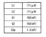
また、各コイルおよびコンデンサにおけるインダクタンスおよび容量の値は、図7に示したように設定した。ここで、コンデンサC1の容量値は、前述した共振周波数f1=100kHz程度となるように設定した。また、コンデンサC2の容量値も、このコンデンサC2と受電コイルL2とからなるLC共振回路における共振周波数=100kHz程度となるように設定した。更に、コンデンサC2pの容量値は、整流回路212が非接続(非動作)状態であると仮定した場合において、前述した共振周波数f2=1MHz程度(≫f1)となるように設定した。
The values of inductance and capacitance in each coil and capacitor were set as shown in FIG. Here, the capacitance value of the capacitor C1 was set to be about the above-described resonance frequency f1 = 100 kHz. The capacitance value of the capacitor C2 was also set so that the resonance frequency in the LC resonance circuit composed of the capacitor C2 and the power receiving coil L2 was about 100 kHz. Further, the capacitance value of the capacitor C2p is set to be the above-described resonance frequency f2 = 1 MHz (>> f1) when it is assumed that the
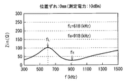
ここで、図8Aおよび図8Bはそれぞれ、実施例1における、位置ずれが無しの場合と有りの場合とについての、入力インピーダンスZinの周波数特性の測定結果を示したものである。また、表1は、位置ずれが無しの場合と有りの場合とについて、実施例1および比較例において求められた結合係数kの値をそれぞれ対比して表したものである。 Here, FIG. 8A and FIG. 8B show the measurement results of the frequency characteristics of the input impedance Zin in the first embodiment when there is no positional deviation and when there is no positional deviation. Table 1 compares the values of the coupling coefficient k obtained in Example 1 and the comparative example with respect to the case where there is no positional deviation and the case where there is no positional deviation.
この表1により、位置ずれが無しの場合と有りの場合との双方について、実施例1において求められた結合係数kの値が、比較例(一般的な手法)において求められた結合係数kの値と略同等のものとなり、精度良く結合係数kが求められていることが分かる。なお、この実施例1では、計算上はfL=1MHzとなるようにコンデンサC2pの容量値を設定しているが、ここでは整流回路212内の寄生容量成分の影響で、計算値よりも低くなっている。
According to Table 1, the value of the coupling coefficient k obtained in Example 1 is the value of the coupling coefficient k obtained in the comparative example (general method) in both cases where there is no positional deviation and in the case where there is no positional deviation. It can be seen that the coupling coefficient k is obtained with high accuracy. In the first embodiment, the capacitance value of the capacitor C2p is set so that f L = 1 MHz in the calculation, but here it is lower than the calculated value due to the influence of the parasitic capacitance component in the
また、図9Aおよび図9Bはそれぞれ、実施例2における、位置ずれが無しの場合と有りの場合とについての、入力インピーダンスZinの周波数特性の測定結果を示したものである。この実施例2では、実施例1と比べて測定電力が大きくなっていることから、測定信号が徐々に微弱信号とはみなせなくなってきた(整流回路212が非動作状態とはみなせなくなってきた)影響で、入力インピーダンスZinにおける極値(山部分およぼ谷部分)がなだらかになっていることが分かる。また、これらの極値時の周波数fL,fHの値についても、実施例1における値とは若干ずれていることが分かる。これらのことから、測定電力をある程度低く抑え、測定信号が微弱信号とみなせる範囲内の条件で、入力インピーダンスZinの周波数特性を測定するようにするのが望ましいと言える。
9A and 9B show the measurement results of the frequency characteristics of the input impedance Zin in the second embodiment when there is no positional deviation and when there is no positional deviation. In the second embodiment, since the measured power is larger than that in the first embodiment, the measurement signal is gradually regarded as a weak signal (the
以上のように本実施の形態では、整流回路212の非動作状態時における入力インピーダンスZinの周波数特性の測定結果を利用して結合係数kを算出するようにしたので、複雑な手法を用いずに結合係数kを得ることができる。よって、磁界を用いて電力伝送を行う際の結合係数kを簡易に求めることが可能となる。
As described above, in the present embodiment, the coupling coefficient k is calculated using the measurement result of the frequency characteristic of the input impedance Zin when the
具体的には、給電装置1側のみでの簡易な制御で、かつ、大型のセンサ等を別途追加することなく、結合係数kを求めることができるため、小型かつ低コストで実現することが可能となる。また、測定手法が簡易であることから、短い測定時間(算出時間)で求めることができる。
Specifically, since the coupling coefficient k can be obtained by simple control only on the
更に、本実施の形態の算出方法では、以下説明する第2の実施の形態における算出方法と比べ、以下の利点も得られる。すなわち、前述したように、2つの共振周波数f1,f2の間で(f1≪f2)の条件を満たしたうえで測定することから、このような測定時の前提条件を比較的容易に成立させることができ、素子のばらつき(コンデンサC2pの容量値のばらつき等)に強い手法とすることができる。 Furthermore, the calculation method according to the present embodiment provides the following advantages as compared with the calculation method according to the second embodiment described below. That is, as described above, since the measurement is performed after satisfying the condition of (f1 << f2) between the two resonance frequencies f1 and f2, it is possible to establish such a precondition at the time of measurement relatively easily. Therefore, it is possible to use a technique that is strong against variations in elements (such as variations in the capacitance value of the capacitor C2p).
<第2の実施の形態>
続いて、本開示の第2の実施の形態について説明する。上記第1の実施の形態では、極小値時および極大値時の双方の周波数を用いて結合係数kを求める場合の例について説明したが、第2の実施の形態では、2つの極小値時の周波数を用いて結合係数kを求める例となっている。なお、第1の実施の形態における構成要素と同一のものには同一の符号を付し、適宜説明を省略する。
<Second Embodiment>
Subsequently, a second embodiment of the present disclosure will be described. In the first embodiment, the example in which the coupling coefficient k is obtained using both the frequency at the minimum value and the frequency at the maximum value has been described. However, in the second embodiment, at the time of two minimum values. In this example, the coupling coefficient k is obtained using the frequency. In addition, the same code | symbol is attached | subjected to the same thing as the component in 1st Embodiment, and description is abbreviate | omitted suitably.
[給電システム4Aの構成]
図10は、本開示の第2の実施の形態に係る給電システム(給電システム4A)の構成例を、回路図およびブロック図で表したものである。本実施の形態の給電システム4Aは、第1の実施の形態の給電システム4において、給電装置1の代わりに以下説明する給電装置1Aを設けたものに対応しており、他の構成は同様となっている。
[Configuration of Power Supply System 4A]
FIG. 10 is a circuit diagram and a block diagram illustrating a configuration example of a power feeding system (power feeding system 4A) according to the second embodiment of the present disclosure. The power feeding system 4A according to the present embodiment corresponds to the power feeding system 4 according to the first embodiment provided with a power feeding device 1A described below instead of the
(給電装置1A)
給電装置1Aは、給電装置1において、コンデンサC1sを更に設けると共に、結合係数算出回路112の代わりに結合係数算出回路112A(結合係数算出部)を設けたものに対応しており、他の構成は同様となっている。
(Power supply device 1A)
The power feeding device 1A corresponds to the
コンデンサC1sは、結合係数算出回路112Aと電力供給ラインLpとの間(この例では、結合係数算出回路112Aとスイッチング素子SW2との間)の経路上に配置されている。このコンデンサC1sは、コンデンサC2pとともに、後述する2つの共振周波数f1,f2間での条件(f1=f2=f0)を満たすようにするために設けられている。
The capacitor C1s is arranged on a path between the coupling
結合係数算出回路112Aは、第1の実施の形態の結合係数算出回路112において、算出・制御部34の代わりに算出・制御部34Aを設けたものに対応しており、他の構成は同様となっている。
The coupling
この算出・制御部34Aは、以下説明するように、基本的には算出・制御部34と同様の手法を用いて、結合係数kを算出している。すなわち、給電対象機器である電子機器2A,2B内の整流回路212の非動作状態時における入力インピーダンスZinの周波数特性を測定し、その周波数特性の測定結果を利用して結合係数kを算出する。
As will be described below, the calculation /
ただし、本実施の形態では第1の実施の形態とは異なり、上記したように、2つの極小値時の周波数を用いて結合係数kを算出する。以下、この手法について詳細に説明する。 However, in the present embodiment, unlike the first embodiment, the coupling coefficient k is calculated using the frequencies at the two minimum values as described above. Hereinafter, this method will be described in detail.
まず、例えば図11中の破線で示したように、結合係数kの算出時(入力インピーダンスZinの周波数特性の測定時)には、本実施の形態においてもバイパス経路Lbおよび微弱信号である測定信号を用いて、整流回路211が自動的に非動作状態となるように構成されている。
First, as shown by a broken line in FIG. 11, for example, when the coupling coefficient k is calculated (when measuring the frequency characteristic of the input impedance Zin), the measurement signal which is the bypass path Lb and the weak signal also in this embodiment. Is used so that the
また、同じく図11中の破線で示したように、この入力インピーダンスZinの周波数特性の測定時には、本実施の形態においても第1の実施の形態と同様にして、交流信号発生回路111もまた非動作状態となるように設定されている。
Similarly, as shown by the broken line in FIG. 11, when measuring the frequency characteristic of the input impedance Zin, the AC
ここで、このようにして整流回路211および交流信号発生回路111がそれぞれ非動作状態に設定された場合、本実施の形態では、入力インピーダンスZinは、以下の(8)〜(12)式により表わされる。なお、これらの式中において、各パラメータは以下の通りである。
L1 : 送電コイルL1のインダクタンス
L2 : 受電コイルL2のインダクタンス
C1 : コンデンサC1の容量
C1s: コンデンサC1sの容量
C1’: コンデンサC1,C1sの合成容量
C2 : コンデンサC2の容量
C2p: コンデンサC2pの容量
C2’: コンデンサC2,C2pの合成容量
f1 : 送電コイルL1とコンデンサC1,C1sとからなるLC共振回路における共振周波数
f2 : 受電コイルL2とコンデンサC2,C2pとからなるLC共振回路における共振周波数
f : 測定時の周波数(測定信号の周波数,可変値)
k : 送電コイルL1と受電コイルL2との間の結合係数
Here, when the
L1: Inductance L2 of power transmission coil L1: Inductance C1 of power reception coil L2: Capacitance C1s of capacitor C1: Capacitance C1 'of capacitor C1s: Combined capacity C2 of capacitors C1 and C1s: Capacitance C2p of capacitor C2p: Capacitance C2' of capacitor C2p : Combined capacitance f1 of capacitors C2 and C2p: Resonance frequency f2 in LC resonance circuit composed of power transmission coil L1 and capacitors C1 and C1s: Resonance frequency f in LC resonance circuit composed of power reception coil L2 and capacitors C2 and C2p: During measurement Frequency (measurement signal frequency, variable value)
k: Coupling coefficient between the power transmission coil L1 and the power reception coil L2
また、上記した2つの共振周波数f1,f2間で、前述したように(f1=f2=f0)の条件を満たすようにコンデンサC1s,C2pの容量が設定されている場合、入力インピーダンスZinの周波数特性は、例えば図12に示したようになる。すなわち、入力インピーダンスZinは、測定信号の周波数fを変化させていった場合に、2つの極値を持つようになる。具体的には、本実施の形態の場合、2つの周波数fL,fHの双方おいて極小値を示す。なお、本実施の形態においても第1の実施の形態と同様に、例えば、送電部110内にコンデンサC1が配置されておらず、送電コイルL1の一端と電力供給ラインLpとが短絡されている場合、容量C1→∞(合成容量C1’=容量C1)とみなせるため、この場合も同様に適用することができる。
Further, when the capacitances of the capacitors C1s and C2p are set so as to satisfy the condition (f1 = f2 = f0) between the two resonance frequencies f1 and f2, as described above, the frequency characteristics of the input impedance Zin. For example, as shown in FIG. That is, the input impedance Zin has two extreme values when the frequency f of the measurement signal is changed. Specifically, in the case of the present embodiment, the minimum value is shown at both of the two frequencies f L and f H. In the present embodiment, as in the first embodiment, for example, the capacitor C1 is not disposed in the
ここで、このような極小値時の周波数fL,fHはそれぞれ、以下の(13)式および(14)式により表わされる。 Here, the frequencies f L and f H at such a minimum value are expressed by the following equations (13) and (14), respectively.
したがって、結合係数算出回路112Aにおいて入力インピーダンスZinの周波数特性を測定し、その測定結果から極小値時の周波数fL,fHの値をそれぞれ検出することで、上記(13),(14)式に基づく以下の(15)式を用いて、結合係数kが求められる。
Therefore, the coupling
以上のように本実施の形態においても、基本的には第1の実施の形態と同様の作用により同様の効果を得ることが可能である。すなわち、磁界を用いて電力伝送を行う際の結合係数kを簡易に求めることが可能となる。 As described above, also in the present embodiment, basically the same effect can be obtained by the same operation as that of the first embodiment. That is, it is possible to easily obtain the coupling coefficient k when performing power transmission using a magnetic field.
また、本実施の形態の算出方法では、前述した第1の実施の形態における算出方法と比べ、以下の利点も得られる。すなわち、周波数特性の測定結果から検出する極値が極小値だけでよいので、極大値および極小値の双方を検出する場合と比べ、入力インピーダンスZinを測定する際のダイナミックレンジが小さくて済むと言える。 In addition, the calculation method according to the present embodiment provides the following advantages as compared with the calculation method according to the first embodiment described above. That is, since the extreme value detected from the measurement result of the frequency characteristic may be only the minimum value, it can be said that the dynamic range when measuring the input impedance Zin is small compared to the case where both the maximum value and the minimum value are detected. .
<変形例1,2>
続いて、上記第1および第2の実施の形態に共通の変形例(変形例1,2)について説明する。これらの変形例1,2は、電子機器2A,2B内におけるバイパス経路Lbの他の配置構成例に対応している。なお、第1,第2の実施の形態における構成要素と同一のものには同一の符号を付し、適宜説明を省略する。
<
Subsequently, modified examples (modified examples 1 and 2) common to the first and second embodiments will be described. These
図13Aは、変形例1に係るバイパス経路Lbの配置構成例を回路図で表わしたものであり、図13Bは、変形例2に係るバイパス経路Lbの配置構成例を回路図で表わしたものである。 FIG. 13A is a circuit diagram illustrating an arrangement configuration example of the bypass path Lb according to the first modification, and FIG. 13B is a circuit diagram illustrating an arrangement configuration example of the bypass path Lb according to the second modification. is there.
図13Aに示した変形例1では、受電部210内にバイパス経路Lbが配置されている。具体的には、受電コイルL2とコンデンサC2との間に、バイパス経路Lbが配置されている。
In the first modification shown in FIG. 13A, the bypass path Lb is arranged in the
一方、図13Bに示した変形例2では、受電部210A内にはコンデンサC2が設けられておらず、この受電部210Aと整流回路211との間にバイパス経路Lbが配置されている。
On the other hand, in the second modification shown in FIG. 13B, the capacitor C2 is not provided in the power receiving unit 210A, and the bypass path Lb is disposed between the power receiving unit 210A and the
このように、電子機器2A,2B内におけるバイパス経路Lbの配置構成としては、整流回路211に対してバイパスする役割を果たすのであれば、種々の配置構成をとることが可能である。また、バイパス経路Lb上のコンデンサC2pとしても、そのような容量素子を積極的に設けるのではなく、寄生容量成分を代わりに用いるようにしてもよい。すなわち、バイパス経路Lb上にコンデンサC2pを設ける代わりに、例えば整流回路211における寄生容量成分を用いて、受電コイルL2とともにLC共振回路を構成するようにしてもよい。このような構成としても、基本的には第1,第2の実施の形態と同様の作用により同様の効果を得ることが可能である。
As described above, as the arrangement configuration of the bypass path Lb in the
なお、例えば変形例1,2のような、バイパス経路Lpの配置構成やコンデンサC2の配置の有無等に応じて、(1)〜(4)式や(8)〜(12)式における合成容量C2’および共振周波数f2はそれぞれ、適宜読み替える必要がある。より一般化した表現にすると、合成容量C2’は、整流回路211の非動作状態において、受電コイルL2とLC共振回路を構成するコンデンサの合成容量であり、共振周波数f2は、そのLC共振回路における共振周波数である。
Note that the combined capacitances in the equations (1) to (4) and (8) to (12) according to the arrangement configuration of the bypass path Lp, the presence or absence of the capacitor C2, etc. Each of C2 ′ and resonance frequency f2 needs to be read as appropriate. In a more generalized expression, the combined capacitance C2 ′ is a combined capacitance of the capacitor that configures the power receiving coil L2 and the LC resonance circuit in the non-operating state of the
<第3の実施の形態>
続いて、本開示の第3の実施の形態について説明する。本実施の形態では、上記第1または第2の実施の形態で説明した手法を用いて求められた結合係数kを利用して、送電(給電)の際のパラメータ(給電パラメータ)を設定する動作について説明する。なお、第1,第2の実施の形態等における構成要素と同一のものには同一の符号を付し、適宜説明を省略する。
<Third Embodiment>
Subsequently, a third embodiment of the present disclosure will be described. In the present embodiment, an operation for setting a parameter (power supply parameter) at the time of power transmission (power supply) using the coupling coefficient k obtained using the method described in the first or second embodiment. Will be described. In addition, the same code | symbol is attached | subjected to the same thing as the component in 1st, 2nd embodiment etc., and description is abbreviate | omitted suitably.
本実施の形態の給電システムは、基本的には第1,第2の実施の形態の給電システム4,4Aと同様である。ここで、上記したように、結合係数算出回路112または結合係数算出回路112Aにより算出された結合係数kを利用して給電パラメータを設定する機能は、主に給電装置1,1A内の制御部114が担っている。すなわち、この制御部114が、本開示における「パラメータ設定部」の一具体例に対応している。
The power feeding system of the present embodiment is basically the same as the power feeding systems 4 and 4A of the first and second embodiments. Here, as described above, the function of setting the power feeding parameter using the coupling coefficient k calculated by the coupling
図14は、本実施の形態に係る給電パラメータの設定動作の一例を流れ図で表わしたものである。この給電パラメータの設定動作は、図14中に示したように、一連の給電動作の際の「待機フェーズ」,「起動・通信フェーズ」,「給電フェーズ」のうちの、起動・通信フェーズおよび給電フェーズにおいてそれぞれ行われるようになっている。 FIG. 14 is a flowchart showing an example of the power supply parameter setting operation according to the present embodiment. As shown in FIG. 14, the power supply parameter setting operation is performed in the start / communication phase and the power supply among the “standby phase”, “startup / communication phase”, and “power supply phase” in a series of power supply operations. It is done in each phase.
この一連の給電動作では、まず、給電装置1,1Aにおいて、各種の手法を用いて物体検知(給電対象機器が近傍に存在するのか否かの検知)を行う(図14のステップS201)。次いで、結合係数算出回路112,112Aは、第1または第2の実施の形態で説明した手法を用いて(ステップS101〜S107)、結合係数kを求める(ステップS202)。
In this series of power supply operations, first, in the
続いて、制御部114は、このようにして求められた結合係数kを利用して、給電対象機器である電子機器2A,2Bが起動する際の給電パラメータ(給電パラメータの初期値)を設定する(ステップS203)。そして、その後、制御部114の制御に従って、送電コイルL1から電子機器2A,2Bに対して起動信号が送信される(ステップS204)。
Subsequently, the
このように、本実施の形態では、結合係数算出回路112,112Aは、給電対象機器である電子機器2A,2Bの起動前に、結合係数kの算出を行う。そして、電子機器2A,2Bの起動信号における給電パラメータを、求められた結合係数kの大きさに応じて変化させるようにしている。具体的には、例えば、起動信号の電圧を、結合係数kに対して反比例の関係を満たす(起動信号の電圧∝(1/k))ように設定する。
As described above, in the present embodiment, the coupling
これは、以下の理由によるものである。すなわち、まず、給電対象機器が起動する際には、ある決められた受電電圧が必要である場合が多い。また、給電対象機器の起動フェーズでは、負荷22は接続されていないため軽負荷であり、その場合、受電電圧は、概ね結合係数kと起動信号の電圧とに比例する(受電電圧∝(k×起動信号の電圧))。そのため、給電対象機器が給電装置1上に置かれた際に、求められた結合係数kを用いて、上記したように起動信号の電圧を結合係数kと反比例するように設定することで、以下の利点が得られる。つまり、給電対象機器が置かれた位置等に関わらず、受電電圧がほぼ一定となり、給電対象機器における安定した起動動作が可能となる。
This is due to the following reason. That is, first, when a power supply target device is activated, a predetermined power reception voltage is often required. Further, in the startup phase of the power supply target device, the
続いて、起動信号が送信されて電子機器2A,2Bが起動すると、給電装置1,1A(1次側機器)と電子機器2A,2B(2次側機器)とにおいて、前述した通信部113,214間での相互の通信が行われる。これにより、電子機器2A,2Bでは、給電パラメータの取得が可能となる(ステップS205)。
Subsequently, when the activation signal is transmitted and the
次に、制御部114は、求められた結合係数kを利用して、電子機器2A,2Bに対して実際に給電する際の給電パラメータを設定する(ステップS206)。そして、このようにして設定された給電パラメータを用いて、給電装置1,1Aから電子機器2A,2Bへの給電(本給電)が開始される(ステップS207)。
Next, using the obtained coupling coefficient k, the
ここで本実施の形態では、制御部114は、求められた結合係数kを用いて、例えば給電の際の周波数(給電周波数,送電周波数)を設定する。具体的には、例えば、給電装置1内および電子機器2A,2B内での共振周波数がいずれもf0であるものとすると、給電周波数=(f0/(1−k)1/2)に設定する。
Here, in the present embodiment, the
これは、以下の理由によるものである。すなわち、まず、負荷22が電力を引いた際の受電電圧の変化量は、給電周波数によって異なるものとなる。また、この受電電圧の変化量が小さいほど、安定した電力伝送であると言える。そして、この給電周波数の値が、上記したように(f0/(1−k)1/2)である場合に、受電電圧の変化量が最も小さくなることが知られている。したがって、求められた結合係数kを用いて給電周波数をこの値に設定することで、受電電圧の変化量が最も小さくなり、安定した電力伝送が可能となる。
This is due to the following reason. That is, first, the amount of change in the received voltage when the
なお、その後は、給電パラメータの再設定(ステップS208)を適宜行い、バッテリー213が満充電状態であるのか否か、あるいは給電が中止となるのか否かが、ユーザからの設定や相互の通信等に従って判断される(ステップS209)。そして、満充電状態ではなく、かつ給電中止とならないと判断された場合には(ステップS209:N)、給電が継続され(ステップS210)、再びステップS208へと戻ることになる。一方、満充電状態であったり、給電中止となると判断された場合には(ステップS209:Y)、給電が停止され(ステップS211)、図14に示した一連の給電動作が終了となる。
After that, resetting of power feeding parameters (step S208) is performed as appropriate so that whether or not the
以上のように本実施の形態では、求められた結合係数kを利用して給電パラメータを設定するようにしたので、例えば、予め決められた固定の給電パラメータではなく、給電対象機器の起動前に求められた結合係数kの大きさに応じて適切な給電パラメータを設定することが可能となる。 As described above, in the present embodiment, since the power supply parameter is set using the obtained coupling coefficient k, for example, it is not a fixed power supply parameter determined in advance, but before starting the power supply target device. An appropriate power supply parameter can be set according to the obtained magnitude of the coupling coefficient k.
また、求められた結合係数kを用いて給電周波数を設定するようにしたので、受電電圧の変化量を最も小さく設定することができ、安定した電力伝送を行うことが可能となる。 In addition, since the power supply frequency is set using the obtained coupling coefficient k, the amount of change in the received voltage can be set to the minimum, and stable power transmission can be performed.
<第4の実施の形態>
続いて、本開示の第4の実施の形態について説明する。本実施の形態では、上記第1または第2の実施の形態で説明した手法を用いて結合係数kを求める際に、併せて給電対象機器が近傍に存在するのか否かを検知する動作(物体検知動作)を行う手法について説明する。なお、第1〜第3の実施の形態等における構成要素と同一のものには同一の符号を付し、適宜説明を省略する。
<Fourth embodiment>
Subsequently, a fourth embodiment of the present disclosure will be described. In the present embodiment, when the coupling coefficient k is obtained using the method described in the first or second embodiment, an operation (object for detecting whether or not a power supply target device exists in the vicinity is also included. A method for performing the detection operation will be described. In addition, the same code | symbol is attached | subjected to the same thing as the component in 1st-3rd embodiment etc., and description is abbreviate | omitted suitably.
本実施の形態の給電システムも、基本的には第1,第2の実施の形態の給電システム4,4Aと同様である。ここで、上記したように、結合係数算出回路112または結合係数算出回路112Aにより算出された結合係数kを利用して物体検知動作を行う機能は、主に給電装置1,1A内の算出・制御部34および制御部114が担っている。
The power feeding system of the present embodiment is basically the same as the power feeding systems 4 and 4A of the first and second embodiments. Here, as described above, the function of performing the object detection operation using the coupling coefficient k calculated by the coupling
図15は、第4の実施の形態に係る結合係数の算出動作および給電対象機器の有無の検知動作の一例を流れ図で表わしたものである。この図15に示した動作において、第1の実施の形態で説明した結合係数の算出動作のみを行う場合と異なる点は、極値時の周波数fL,fHの値をそれぞれ検出した後に、その結果を利用して物体検知動作をも行うようにした点である。つまり、結合係数算出部112,112A等は、入力インピーダンスZinの周波数特性の測定結果を利用して、給電対象機器が近傍に存在するのか否かの検知をも行うようになっている。
FIG. 15 is a flowchart illustrating an example of the coupling coefficient calculation operation and the power supply target device detection operation according to the fourth embodiment. The operation shown in FIG. 15 differs from the case where only the coupling coefficient calculation operation described in the first embodiment is performed, after the values of the frequencies f L and f H at the extreme values are detected, respectively. The object detection operation is also performed using the result. That is, the coupling
具体的には、この図15に示した動作例では、図6に示した動作例において、以下のようにしたものとなっている。すなわち、ステップS106において、極値およびその時の周波数fL,fHの双方を検出するようにすると共に、その後に以下説明するステップS111〜S113の動作を更に追加したものとなっている。 Specifically, in the operation example shown in FIG. 15, the operation example shown in FIG. 6 is as follows. That is, in step S106, both the extreme value and the frequencies f L and f H at that time are detected, and then the operations of steps S111 to S113 described below are further added.
具体的には、極値およびその時の周波数fL,fHがそれぞれ検出された後、結合係数算出部112,112A等は、この検出結果(例えば、周波数fL,fHの値や、その周波数時における入力インピーダンスZinの値等)が予め設定された所定の範囲内にあるのか否かを判定する(ステップS111)。
Specifically, after the extreme values and the frequencies f L and f H at that time are detected, the
ここで、この検出結果が所定の範囲内にあると判定された場合(ステップS111:Y)、結合係数算出部112,112A等は、想定された給電対象機器が給電装置1の近傍に存在すると判定する(ステップS112)。そして、その後は前述したステップS107(結合係数kの算出)へと移行する。
Here, when it is determined that the detection result is within the predetermined range (step S111: Y), the coupling
一方、検出結果が所定の範囲内にはないと判定された場合(ステップS111:N)、結合係数算出部112,112A等は、想定された給電対象機器が給電装置1の近傍には存在しないと判定する(ステップS113)。このため、この場合には結合係数kの算出は行われず、図15に示した動作が終了となる。ここで、このような判定ができるのは、例えば硬貨等の金属異物や他方式の非接触給電機器等が近傍に位置する場合、入力インピーダンスZinの周波数特性の測定結果が、予め設定された所定の範囲内には入らないためである。
On the other hand, when it is determined that the detection result is not within the predetermined range (step S111: N), the coupling
以上のように本実施の形態では、入力インピーダンスZinの周波数特性の測定結果を利用して、給電対象機器が近傍に存在するのか否かの検知をも行うようにしたので、結合係数算出機能を物体検知機能としても用いることが可能となる。すなわち、結合係数kを算出する際に併せて物体検知をも行うことができ、両機能を別々のモジュールにて実現する場合と比べ、装置構成の簡素化・小型化・低コスト化を図ることが可能となる。 As described above, in the present embodiment, the measurement result of the frequency characteristic of the input impedance Zin is used to detect whether or not the power supply target device exists in the vicinity. It can also be used as an object detection function. In other words, it is possible to perform object detection when calculating the coupling coefficient k, and to simplify, reduce the size, and reduce the cost of the device configuration as compared with the case where both functions are realized by separate modules. Is possible.
<第5の実施の形態>
続いて、本開示の第5の実施の形態について説明する。本実施の形態では、上記第1または第2の実施の形態で説明した手法を用いて求められた結合係数kを利用して、送電制御(給電の可否の判断等)を行う手法について説明する。なお、第1〜第4の実施の形態等における構成要素と同一のものには同一の符号を付し、適宜説明を省略する。
<Fifth embodiment>
Subsequently, a fifth embodiment of the present disclosure will be described. In the present embodiment, a method for performing power transmission control (determination of whether or not to supply power) using the coupling coefficient k obtained using the method described in the first or second embodiment will be described. . In addition, the same code | symbol is attached | subjected to the same thing as the component in 1st-4th embodiment etc., and description is abbreviate | omitted suitably.
本実施の形態の給電システムも、基本的には第1,第2の実施の形態の給電システム4,4Aと同様である。ここで、上記したように、結合係数算出回路112または結合係数算出回路112Aにより算出された結合係数kを利用して送電制御を行う機能は、主に給電装置1,1A内の制御部114が担っている。すなわち、この制御部114が、本開示における「送電制御部」の一具体例に対応している。
The power feeding system of the present embodiment is basically the same as the power feeding systems 4 and 4A of the first and second embodiments. Here, as described above, the function of performing power transmission control using the coupling coefficient k calculated by the coupling
図16は、第5の実施の形態に係る送電制御動作の一例を流れ図で表わしたものである。この送電制御動作では、まず待機フェーズにおいて、前述した物体検知(ステップS201)および結合係数kの算出(ステップS202)が行われる。 FIG. 16 is a flowchart illustrating an example of the power transmission control operation according to the fifth embodiment. In this power transmission control operation, first, in the standby phase, the aforementioned object detection (step S201) and calculation of the coupling coefficient k (step S202) are performed.
次いで、制御部114は、このようにして求められた結合係数kの大きさに応じて、送電動作を制御する。具体的には、この例では制御部114は、まず、結合係数kの値が所定の閾値kth1(第1閾値)よりも大きいのか否か(k>kth1を満たすのか否か)を判定する(ステップS221)。
Next, the
ここで、結合係数kの値がこの閾値kth1以下(k≦kth1)であると判定された場合(ステップS221:N)には、制御部114は、例えば交流信号発生回路111等の動作を停止させることで、送電コイルL1から送電が実行されないように制御する。具体的には、この場合にはステップS201へと戻り、その後の起動・通信フェーズ(前述したステップS203〜S205)および給電フェーズ(前述したステップS206〜S210)等へ移行しないようにする。
Here, when it is determined that the value of the coupling coefficient k is equal to or less than the threshold value kth1 (k ≦ kth1) (step S221: N), the
一方、結合係数kの値が閾値kth1よりも大きい(k>kth1)と判定された場合(ステップS221:Y)には、制御部114は、その後に送電コイルL1から送電が実行されるように制御する。すなわち、その後の起動・通信フェーズおよび給電フェーズ等へは移行するようにする。
On the other hand, when it is determined that the value of the coupling coefficient k is larger than the threshold value kth1 (k> kth1) (step S221: Y), the
このようにして、求められた結合係数kの値が小さい(k≦kth1)場合に、その後の送電が実行されないように送電制御を行うことで、非接触給電の際に発生する発熱や不要輻射等を低減もしくは抑止することが可能となる。これは、以下の理由によるものである。 In this way, when the value of the obtained coupling coefficient k is small (k ≦ kth1), by performing power transmission control so that subsequent power transmission is not performed, heat generation and unnecessary radiation generated during non-contact power feeding are performed. Etc. can be reduced or suppressed. This is due to the following reason.
すなわち、まず、結合係数kの値が小さい場合、給電対象機器おいて同じ受電電圧を発生させるには、送電コイルL1に流す電流を大きくする必要があるため、給電装置での発熱が増大する。また、それに伴って給電対象機器の筐体を貫く磁束も増大するため、渦電流損により、給電対象機器での発熱も増大する。一方、不要輻射に関しても、結合係数kの値が小さいと増大する傾向にある。そこで、上記したように、求められた結合係数kの値が小さい場合に、その後の送電が実行されないように送電制御を行うことで、発熱や不要輻射等を低減もしくは抑止することが可能となる。 That is, first, when the value of the coupling coefficient k is small, in order to generate the same power reception voltage in the power supply target device, it is necessary to increase the current flowing through the power transmission coil L1, so heat generation in the power supply device increases. Moreover, since the magnetic flux which penetrates the housing | casing of the electric power supply object apparatus also increases in connection with it, the heat_generation | fever in an electric power supply object apparatus also increases by eddy current loss. On the other hand, unnecessary radiation also tends to increase when the value of the coupling coefficient k is small. Therefore, as described above, when the value of the obtained coupling coefficient k is small, by performing power transmission control so that subsequent power transmission is not performed, it becomes possible to reduce or suppress heat generation, unnecessary radiation, and the like. .
ここで本実施の形態では、例えば図17に示した送電制御動作のようにしてもよい。すなわち、結合係数kの値が閾値kth1よりも大きい(k>kth1)と判定された場合(ステップS221:Y)において、更に、その結合係数kの値がもう1つの別の閾値kth2(>kth1)(第2の閾値)以下であるのか否か(k≦kth2を満たすのか否か)を判定する(ステップS222)ようにしてもよい。 Here, in the present embodiment, for example, the power transmission control operation shown in FIG. 17 may be performed. That is, when it is determined that the value of the coupling coefficient k is larger than the threshold value kth1 (k> kth1) (step S221: Y), the value of the coupling coefficient k is further set to another threshold value kth2 (> kth1). ) (Second threshold) or less (whether k ≦ kth2 is satisfied) may be determined (step S222).
ここで、結合係数kの値が更にこの閾値kth2よりも大きい(k>kth2)と判定された場合(ステップS222:N)には、制御部114は、その後に送電コイルL1から送電が実行されるように制御する。すなわち、その後の起動・通信フェーズおよび給電フェーズ等へは移行するようにする。
Here, when it is determined that the value of the coupling coefficient k is further larger than the threshold value kth2 (k> kth2) (step S222: N), the
一方、結合係数kの値が、閾値kth1よりは大きいものの閾値kth2以下(kth2≧k>kth1)である場合(ステップS222:Y)には、制御部114は以下の送電制御を行う。すなわち、制御部114は、給電対象機器における受電電力を下げる制御(受電電力の低減制御;ステップS223)が行われた後に、その後の起動・通信フェーズおよび給電フェーズ等へは移行するようにする。このような送電制御を行うようにした場合、受電電力の適切な制御も可能となり、発熱や不要輻射等の更なる低減もしくは抑止が可能となる。
On the other hand, when the value of the coupling coefficient k is larger than the threshold value kth1 but not more than the threshold value kth2 (kth2 ≧ k> kth1) (step S222: Y), the
ここで、上記したような受電電力の低減制御の手法としては、例えば以下の(A),(B)の2つの手法が挙げられる。
(A)求められた結合係数kの情報を通信によって給電装置1から給電対象機器へと送信し、給電対象機器側において、受電電力の決定および制御を行う。
(B)求められた結合係数kに基づいて、給電装置1側において受電電力を決定し、その受電電力の情報を通信によって給電対象機器へと送信し、給電対象機器側で受電電力の制御を行う。
Here, the following two methods (A) and (B) can be cited as examples of the method for reducing the received power as described above.
(A) Information on the obtained coupling coefficient k is transmitted from the
(B) Based on the obtained coupling coefficient k, the received power is determined on the
以上のように本実施の形態では、求められた結合係数kを利用して、送電制御(給電の可否の判断等)を行うようにしたので、発熱や不要輻射等を低減もしくは抑止することが可能となる。 As described above, in this embodiment, power transmission control (judgment of power supply availability, etc.) is performed using the obtained coupling coefficient k, so that heat generation, unnecessary radiation, etc. can be reduced or suppressed. It becomes possible.
<その他の変形例>
以上、実施の形態および変形例を挙げて本開示の技術を説明したが、本技術はこれらの実施の形態等に限定されず、種々の変形が可能である。
<Other variations>
As described above, the technology of the present disclosure has been described with reference to the embodiment and the modifications. However, the technology is not limited to the embodiment and the like, and various modifications can be made.
例えば、上記実施の形態等では各種のコイル(送電コイル,受電コイル)を挙げて説明しているが、これらのコイルの構成(形状)としては種々のものを用いることが可能である。すなわち、例えばスパイラル形状やループ形状、磁性体を用いたバー形状、スパイラルコイルを2層で折り返すように配置するα巻き形状、更なる多層のスパイラル形状、厚み方向に巻線が巻回しているヘリカル形状などによって、各コイルを構成することが可能である。また、各コイルは、導電性を有する線材により構成された巻き線コイルだけではなく、プリント基板やフレキシブルプリント基板などにより構成された、導電性を有するパターンコイルであってもよい。 For example, although various embodiments (power transmission coil, power reception coil) have been described in the above-described embodiments, various configurations (shapes) of these coils can be used. That is, for example, spiral shape and loop shape, bar shape using magnetic material, α winding shape that spiral coils are folded in two layers, further multilayer spiral shape, helical with winding wound in the thickness direction Each coil can be configured depending on the shape and the like. Moreover, each coil may be not only a wound coil made of a conductive wire, but also a conductive pattern coil made of a printed board, a flexible printed board, or the like.
また、上記実施の形態等では、給電対象機器の一例として電子機器を挙げて説明したが、これには限られず、電子機器以外の給電対象機器(例えば、電気自動車等の車両など)であってもよい。 Moreover, in the said embodiment etc., although the electronic device was mentioned and demonstrated as an example of electric power feeding object apparatus, it is not restricted to this, It is electric power feeding object apparatuses (for example, vehicles, such as an electric vehicle) other than an electronic device, Also good.
更に、上記実施の形態等では、給電装置および電子機器の各構成要素を具体的に挙げて説明したが、全ての構成要素を備える必要はなく、また、他の構成要素を更に備えていてもよい。例えば、給電装置や電子機器内に、通信機能や何かしらの制御機能、表示機能、2次側機器を認証する機能、異種金属などの混入を検知する機能などを搭載するようにしてもよい。また、結合係数算出回路の構成や算出手法についても、上記実施の形態で説明したものには限られず、他の構成や算出手法であってもよい。更に、入力インピーダンスZinを測定する際の電源として、上記実施の形態等で説明した測定信号発生部の代わりに、例えば給電用のドライバ(上記実施の形態等で説明した交流信号発生回路)を用いるようにしてもよい。 Furthermore, in the above-described embodiment and the like, the respective components of the power feeding device and the electronic device have been specifically described, but it is not necessary to include all the components, and other components may be further included. Good. For example, a communication function, some control function, a display function, a function to authenticate a secondary device, a function to detect mixing of a dissimilar metal, or the like may be installed in the power supply apparatus or the electronic device. Also, the configuration and calculation method of the coupling coefficient calculation circuit are not limited to those described in the above embodiment, and other configurations and calculation methods may be used. Furthermore, as a power source for measuring the input impedance Zin, for example, a power supply driver (an AC signal generation circuit described in the above embodiment) is used instead of the measurement signal generation unit described in the above embodiment. You may do it.
加えて、上記実施の形態等では、整流回路を非動作状態とする際に、微弱信号である測定信号を用いて実現しているが、これには限られず、他の手法を用いて実現するようにしてもよい。すなわち、例えば、整流回路の前段または後段にスイッチを設け、このスイッチをオフ状態に設定することで、整流回路を非動作状態とするようにしてもよい。あるいは、例えば、整流機能の有効状態・無効状態を切替可能な整流回路を設け、給電対象機器内の制御部においてその切り替えを制御することで、整流回路を非動作状態とするようにしてもよい。 In addition, in the above-described embodiment and the like, when the rectifier circuit is brought into a non-operating state, the measurement signal that is a weak signal is used. However, the present invention is not limited to this, and other methods are used. You may do it. That is, for example, a switch may be provided before or after the rectifier circuit, and the switch may be set to an off state so that the rectifier circuit is in an inoperative state. Alternatively, for example, a rectifier circuit that can switch between a valid state and an invalid state of the rectification function may be provided, and the rectifier circuit may be set in a non-operating state by controlling the switching in a control unit in the power supply target device. .
また、上記実施の形態等では、主に、給電システム内に複数(2つ)の電子機器が設けられている場合を例に挙げて説明したが、この場合には限られず、給電システム内に1つの電子機器のみが設けられているようにしてもよい。 Further, in the above-described embodiment and the like, the case where a plurality (two) of electronic devices are mainly provided in the power feeding system has been described as an example, but the present invention is not limited to this case. Only one electronic device may be provided.
更に、上記実施の形態等では、給電装置の一例として、携帯電話機等の小型の電子機器(CE機器)向けの充電トレーを挙げて説明したが、給電装置としてはそのような家庭用の充電トレーには限定されず、様々な電子機器等の充電器として適用可能である。また、必ずしもトレーである必要はなく、例えば、いわゆるクレードル等の電子機器用のスタンドであってもよい。 Further, in the above-described embodiment and the like, a charging tray for a small electronic device (CE device) such as a cellular phone has been described as an example of a power feeding device. However, as a power feeding device, such a household charging tray is used. It is not limited to, but can be applied as a charger for various electronic devices. Further, it is not necessarily a tray, and may be a stand for an electronic device such as a so-called cradle.
なお、本技術は以下のような構成を取ることも可能である。
(1)
磁界を用いた送電を行うための送電コイルと、
前記送電コイルと給電対象機器内の受電コイルとの間の結合係数を算出する結合係数算出部と
を備え、
前記結合係数算出部は、
前記給電対象機器内の整流回路の非動作状態時における入力インピーダンスの周波数特性を測定し、その周波数特性の測定結果を利用して前記結合係数を算出する
給電装置。
(2)
前記結合係数算出部は、
前記周波数特性の測定結果から、前記入力インピーダンスの極値時の周波数を検出し、
その極値時の周波数を用いて前記結合係数を算出する
上記(1)に記載の給電装置。
(3)
前記結合係数算出部は、
前記極値時の周波数として、極小値時の周波数と極大値時の周波数との双方を検出し、
それら双方の周波数を用いて前記結合係数を算出する
上記(2)に記載の給電装置。
(4)
前記送電コイルを含む共振回路における共振周波数をf1、前記受電コイルを含む共振回路における共振周波数をf2としたとき、
(f1≪f2)を満たすように設定されている
上記(3)に記載の給電装置。
(5)
前記結合係数算出部は、
前記極値時の周波数として、2つの極小値時の周波数を検出し、
それら2つの極小値時の周波数を用いて前記結合係数を算出する
上記(2)に記載の給電装置。
(6)
前記送電コイルを含む共振回路における共振周波数をf1、前記受電コイルを含む共振回路における共振周波数をf2としたとき、
(f1=f2)を満たすように設定されている
上記(5)に記載の給電装置。
(7)
前記結合係数算出部は、微弱信号を用いて前記周波数特性を測定することにより、前記整流回路の非動作状態時における前記周波数特性の測定を行う
上記(1)ないし(6)のいずれかに記載の給電装置。
(8)
前記給電対象機器内における前記整流回路に対するバイパス経路上を前記微弱信号が通ることにより、前記整流回路が非動作状態となる
上記(7)に記載の給電装置。
(9)
前記整流回路における一対の入力端子間に前記バイパス経路が配置されると共に、
前記バイパス経路上に容量素子または寄生容量成分が設けられている
上記(8)に記載の給電装置。
(10)
前記送電を行うための交流信号を前記送電コイルへ供給する交流信号発生部を備え、
前記周波数特性を測定する際には、前記整流回路に加えて前記交流信号発生部も非動作状態となっている
上記(1)ないし(9)のいずれかに記載の給電装置。
(11)
前記結合係数算出部は、
前記周波数特性を測定するための測定信号を発生させる測定信号発生部と、
前記送電コイルに流れる電流を検出する電流検出部と、
前記測定信号の電圧および周波数をそれぞれ制御する制御部と、
前記電流検出部により検出された電流と前記制御部により設定された電圧とに基づいて前記入力インピーダンスを算出する算出部と
を有し、
前記制御部が前記測定信号の周波数を連続的に変化させていくことにより、前記算出部において前記周波数特性が得られる
上記(1)ないし(10)のいずれかに記載の給電装置。
(12)
前記結合係数算出部により算出された結合係数を利用して、前記送電の際のパラメータを設定するパラメータ設定部を備えた
上記(1)ないし(11)のいずれかに記載の給電装置。
(13)
前記結合係数算出部は、前記給電対象機器の起動前に前記結合係数の算出を行い、
前記パラメータ設定部は、前記給電対象機器の起動信号におけるパラメータを、前記結合係数算出部により算出された結合係数の大きさに応じて変化させる
上記(12)に記載の給電装置。
(14)
前記パラメータ設定部は、前記起動信号の電圧を、前記結合係数に対して反比例の関係を満たすように設定する
上記(13)に記載の給電装置。
(15)
前記パラメータ設定部は、前記結合係数算出部により算出された結合係数を用いて、前記送電の際の送電周波数を設定する
上記(12)ないし(14)のいずれかに記載の給電装置。
(16)
前記結合係数算出部は、前記周波数特性の測定結果を利用して、前記給電対象機器が近傍に存在するのか否かの検知をも行う
上記(1)ないし(15)のいずれかに記載の給電装置。
(17)
前記結合係数算出部は、前記周波数特性の測定結果が所定の範囲内にあるのか否かによって、前記給電対象機器が近傍に存在するのか否かを検知する
上記(16)に記載の給電装置。
(18)
前記結合係数算出部により算出された結合係数の大きさに応じて、前記送電の際の動作を制御する送電制御部を備え、
前記送電制御部は、前記結合係数が第1閾値以下である場合には、前記送電を実行しない
上記(1)ないし(17)のいずれかに記載の給電装置。
(19)
前記送電制御部は、
前記結合係数が前記第1閾値よりも大きくかつ第2閾値以下である場合には、
前記給電対象機器における受電電力を下げる制御が行われた後に、前記送電を実行する
上記(18)に記載の給電装置。
(20)
受電コイルおよび整流回路を有する1または複数の電子機器と、
前記電子機器に対して磁界を用いた送電を行う給電装置と
を備え、
前記給電装置は、
前記送電を行うための送電コイルと、
前記送電コイルと前記受電コイルとの間の結合係数を算出する算出部と
を有し、
前記算出部は、
前記整流回路の非動作状態時における入力インピーダンスの周波数特性を測定し、その周波数特性の測定結果を利用して前記結合係数を算出する
給電システム。
In addition, this technique can also take the following structures.
(1)
A power transmission coil for performing power transmission using a magnetic field;
A coupling coefficient calculation unit for calculating a coupling coefficient between the power transmission coil and a power receiving coil in the power supply target device,
The coupling coefficient calculation unit includes:
A power feeding device that measures a frequency characteristic of an input impedance when the rectifier circuit in the power supply target device is not operating, and calculates the coupling coefficient using a measurement result of the frequency characteristic.
(2)
The coupling coefficient calculation unit includes:
From the measurement result of the frequency characteristic, the frequency at the extreme value of the input impedance is detected,
The power feeding device according to (1), wherein the coupling coefficient is calculated using a frequency at the extreme value.
(3)
The coupling coefficient calculation unit includes:
As the frequency at the extreme value, both the frequency at the minimum value and the frequency at the maximum value are detected,
The power feeding device according to (2), wherein the coupling coefficient is calculated using both frequencies.
(4)
When the resonance frequency in the resonance circuit including the power transmission coil is f1, and the resonance frequency in the resonance circuit including the power reception coil is f2,
The power feeding device according to (3), which is set to satisfy (f1 << f2).
(5)
The coupling coefficient calculation unit includes:
As the frequency at the extreme value, two frequencies at the minimum value are detected,
The power feeding device according to (2), wherein the coupling coefficient is calculated using a frequency at the time of the two minimum values.
(6)
When the resonance frequency in the resonance circuit including the power transmission coil is f1, and the resonance frequency in the resonance circuit including the power reception coil is f2,
The power feeding device according to (5), which is set to satisfy (f1 = f2).
(7)
The coupling coefficient calculation unit measures the frequency characteristic when the rectifier circuit is in an inoperative state by measuring the frequency characteristic using a weak signal, according to any one of (1) to (6). Power supply device.
(8)
The power feeding apparatus according to (7), wherein the weak signal passes through a bypass path with respect to the rectifying circuit in the power feeding target device, so that the rectifying circuit becomes inoperative.
(9)
The bypass path is disposed between a pair of input terminals in the rectifier circuit,
The power feeding device according to (8), wherein a capacitive element or a parasitic capacitance component is provided on the bypass path.
(10)
An AC signal generator for supplying an AC signal for performing power transmission to the power transmission coil;
The power feeding device according to any one of (1) to (9), wherein when measuring the frequency characteristic, the AC signal generation unit is in a non-operating state in addition to the rectifying circuit.
(11)
The coupling coefficient calculation unit includes:
A measurement signal generator for generating a measurement signal for measuring the frequency characteristic;
A current detection unit for detecting a current flowing in the power transmission coil;
A control unit for controlling the voltage and frequency of the measurement signal, and
A calculation unit that calculates the input impedance based on a current detected by the current detection unit and a voltage set by the control unit;
The power supply device according to any one of (1) to (10), wherein the frequency characteristic is obtained in the calculation unit when the control unit continuously changes the frequency of the measurement signal.
(12)
The power feeding device according to any one of (1) to (11), further including a parameter setting unit configured to set a parameter for the power transmission using the coupling coefficient calculated by the coupling coefficient calculation unit.
(13)
The coupling coefficient calculation unit calculates the coupling coefficient before starting the power supply target device,
The power supply apparatus according to (12), wherein the parameter setting unit changes a parameter in the activation signal of the power supply target device according to the magnitude of the coupling coefficient calculated by the coupling coefficient calculation unit.
(14)
The power supply apparatus according to (13), wherein the parameter setting unit sets the voltage of the activation signal so as to satisfy an inversely proportional relationship with respect to the coupling coefficient.
(15)
The power supply apparatus according to any one of (12) to (14), wherein the parameter setting unit sets a power transmission frequency at the time of power transmission using the coupling coefficient calculated by the coupling coefficient calculation unit.
(16)
The coupling coefficient calculation unit also detects whether or not the power supply target device exists in the vicinity using the measurement result of the frequency characteristic. The power supply according to any one of (1) to (15) apparatus.
(17)
The power supply apparatus according to (16), wherein the coupling coefficient calculation unit detects whether or not the power supply target device exists in the vicinity based on whether or not the measurement result of the frequency characteristic is within a predetermined range.
(18)
According to the magnitude of the coupling coefficient calculated by the coupling coefficient calculation unit, comprising a power transmission control unit that controls the operation during the power transmission,
The power transmission control unit does not execute the power transmission when the coupling coefficient is equal to or less than a first threshold. The power feeding device according to any one of (1) to (17).
(19)
The power transmission control unit
If the coupling coefficient is greater than the first threshold and less than or equal to the second threshold,
The power feeding apparatus according to (18), wherein the power transmission is performed after control for reducing received power in the power supply target device is performed.
(20)
One or more electronic devices having a receiving coil and a rectifying circuit;
A power feeding device that performs power transmission using a magnetic field to the electronic device,
The power supply device
A power transmission coil for performing the power transmission;
A calculation unit for calculating a coupling coefficient between the power transmission coil and the power reception coil,
The calculation unit includes:
A power feeding system that measures a frequency characteristic of an input impedance when the rectifier circuit is not operating, and calculates the coupling coefficient using a measurement result of the frequency characteristic.
1,1A…給電装置、11…送電装置、110…送電部、111…交流信号発生回路、112,112A…結合係数算出回路、113…通信部、114…制御部、2A,2B…電子機器、21…受電装置、210,210A…受電部、211…整流回路、212…給電・充電制御回路、213…バッテリー、214…通信部、215…制御部、22…負荷、30…測定信号発生部、31…電流検出回路、32…アンプ、33…A/D変換器、34,34A…算出・制御部、4,4A…給電システム、9…外部電源、S1…送電面、L1…送電コイル、L2…受電コイル、C1,C1s,C2,C2p,C3…コンデンサ、D1〜D4…整流素子、SW1,SW2…スイッチング素子、Sdc…直流信号、Sac…交流信号、CTL…制御信号、Lp…電力供給ライン、Lb…バイパス経路、I,I(fL),I(fH)…電流、f,fL,fH…周波数、V…電圧、Zin…入力インピーダンス、k…結合係数、kth1,kth2…閾値。
DESCRIPTION OF
Claims (20)
前記送電コイルと給電対象機器内の受電コイルとの間の結合係数を算出する結合係数算出部と
を備え、
前記結合係数算出部は、前記給電対象機器内の整流回路の非動作状態時における入力インピーダンスの周波数特性を測定し、その周波数特性の測定結果を利用して前記結合係数を算出する
給電装置。 A power transmission coil for performing power transmission using a magnetic field;
A coupling coefficient calculation unit for calculating a coupling coefficient between the power transmission coil and a power receiving coil in the power supply target device,
The coupling coefficient calculation unit measures a frequency characteristic of an input impedance when the rectifier circuit in the power supply target device is not operating, and calculates the coupling coefficient using a measurement result of the frequency characteristic.
前記周波数特性の測定結果から、前記入力インピーダンスの極値時の周波数を検出し、
その極値時の周波数を用いて前記結合係数を算出する
請求項1に記載の給電装置。 The coupling coefficient calculation unit includes:
From the measurement result of the frequency characteristic, the frequency at the extreme value of the input impedance is detected,
The power feeding apparatus according to claim 1, wherein the coupling coefficient is calculated using a frequency at the extreme value.
前記極値時の周波数として、極小値時の周波数と極大値時の周波数との双方を検出し、
それら双方の周波数を用いて前記結合係数を算出する
請求項2に記載の給電装置。 The coupling coefficient calculation unit includes:
As the frequency at the extreme value, both the frequency at the minimum value and the frequency at the maximum value are detected,
The power feeding device according to claim 2, wherein the coupling coefficient is calculated using both frequencies.
(f1≪f2)を満たすように設定されている
請求項3に記載の給電装置。 When the resonance frequency in the resonance circuit including the power transmission coil is f1, and the resonance frequency in the resonance circuit including the power reception coil is f2,
The power feeding device according to claim 3, wherein the power feeding device is set to satisfy (f1 << f2).
前記極値時の周波数として、2つの極小値時の周波数を検出し、
それら2つの極小値時の周波数を用いて前記結合係数を算出する
請求項2に記載の給電装置。 The coupling coefficient calculation unit includes:
As the frequency at the extreme value, two frequencies at the minimum value are detected,
The power feeding device according to claim 2, wherein the coupling coefficient is calculated using a frequency at the time of the two minimum values.
(f1=f2)を満たすように設定されている
請求項5に記載の給電装置。 When the resonance frequency in the resonance circuit including the power transmission coil is f1, and the resonance frequency in the resonance circuit including the power reception coil is f2,
The power feeding device according to claim 5, wherein the power feeding device is set to satisfy (f1 = f2).
請求項1に記載の給電装置。 The power supply apparatus according to claim 1, wherein the coupling coefficient calculation unit measures the frequency characteristic when the rectifier circuit is not operating by measuring the frequency characteristic using a weak signal.
請求項7に記載の給電装置。 The power supply apparatus according to claim 7, wherein the weak signal passes through a bypass path to the rectifier circuit in the power supply target device, whereby the rectifier circuit is in an inoperative state.
前記バイパス経路上に容量素子または寄生容量成分が設けられている
請求項8に記載の給電装置。 The bypass path is disposed between a pair of input terminals in the rectifier circuit,
The power feeding device according to claim 8, wherein a capacitive element or a parasitic capacitance component is provided on the bypass path.
前記周波数特性を測定する際には、前記整流回路に加えて前記交流信号発生部も非動作状態となっている
請求項1に記載の給電装置。 An AC signal generator for supplying an AC signal for performing power transmission to the power transmission coil;
The power feeding device according to claim 1, wherein when measuring the frequency characteristic, the AC signal generation unit is also in a non-operating state in addition to the rectifier circuit.
前記周波数特性を測定するための測定信号を発生させる測定信号発生部と、
前記送電コイルに流れる電流を検出する電流検出部と、
前記測定信号の電圧および周波数をそれぞれ制御する制御部と、
前記電流検出部により検出された電流と前記制御部により設定された電圧とに基づいて前記入力インピーダンスを算出する算出部と
を有し、
前記制御部が前記測定信号の周波数を連続的に変化させていくことにより、前記算出部において前記周波数特性が得られる
請求項1に記載の給電装置。 The coupling coefficient calculation unit includes:
A measurement signal generator for generating a measurement signal for measuring the frequency characteristic;
A current detection unit for detecting a current flowing in the power transmission coil;
A control unit for controlling the voltage and frequency of the measurement signal, and
A calculation unit that calculates the input impedance based on a current detected by the current detection unit and a voltage set by the control unit;
The power supply device according to claim 1, wherein the frequency characteristic is obtained in the calculation unit when the control unit continuously changes the frequency of the measurement signal.
請求項1に記載の給電装置。 The power feeding device according to claim 1, further comprising: a parameter setting unit that sets a parameter for power transmission using the coupling coefficient calculated by the coupling coefficient calculation unit.
前記パラメータ設定部は、前記給電対象機器の起動信号におけるパラメータを、前記結合係数算出部により算出された結合係数の大きさに応じて変化させる
請求項12に記載の給電装置。 The coupling coefficient calculation unit calculates the coupling coefficient before starting the power supply target device,
The power supply device according to claim 12, wherein the parameter setting unit changes a parameter in the activation signal of the power supply target device according to the magnitude of the coupling coefficient calculated by the coupling coefficient calculation unit.
請求項13に記載の給電装置。 The power feeding device according to claim 13, wherein the parameter setting unit sets the voltage of the activation signal so as to satisfy an inversely proportional relationship with respect to the coupling coefficient.
請求項12に記載の給電装置。 The power feeding device according to claim 12, wherein the parameter setting unit sets a power transmission frequency during the power transmission using the coupling coefficient calculated by the coupling coefficient calculation unit.
請求項1に記載の給電装置。 The power supply apparatus according to claim 1, wherein the coupling coefficient calculation unit also detects whether or not the power supply target device exists in the vicinity using the measurement result of the frequency characteristic.
請求項16に記載の給電装置。 The power supply apparatus according to claim 16, wherein the coupling coefficient calculation unit detects whether or not the power supply target device exists in the vicinity based on whether or not the measurement result of the frequency characteristic is within a predetermined range.
前記送電制御部は、前記結合係数が第1閾値以下である場合には、前記送電を実行しない
請求項1に記載の給電装置。 According to the magnitude of the coupling coefficient calculated by the coupling coefficient calculation unit, comprising a power transmission control unit that controls the operation during the power transmission,
The power feeding device according to claim 1, wherein the power transmission control unit does not perform the power transmission when the coupling coefficient is equal to or less than a first threshold.
前記結合係数が前記第1閾値よりも大きくかつ第2閾値以下である場合には、
前記給電対象機器における受電電力を下げる制御が行われた後に、前記送電を実行する
請求項18に記載の給電装置。 The power transmission control unit
If the coupling coefficient is greater than the first threshold and less than or equal to the second threshold,
The power feeding apparatus according to claim 18, wherein the power transmission is executed after control for reducing received power in the power supply target device is performed.
前記電子機器に対して磁界を用いた送電を行う給電装置と
を備え、
前記給電装置は、
前記送電を行うための送電コイルと、
前記送電コイルと前記受電コイルとの間の結合係数を算出する結合係数算出部と
を有し、
前記結合係数算出部は、前記整流回路の非動作状態時における入力インピーダンスの周波数特性を測定し、その周波数特性の測定結果を利用して前記結合係数を算出する
給電システム。 One or more electronic devices having a receiving coil and a rectifying circuit;
A power feeding device that performs power transmission using a magnetic field to the electronic device,
The power supply device
A power transmission coil for performing the power transmission;
A coupling coefficient calculation unit that calculates a coupling coefficient between the power transmission coil and the power reception coil;
The power supply system, wherein the coupling coefficient calculation unit measures a frequency characteristic of an input impedance when the rectifier circuit is not operating, and calculates the coupling coefficient using a measurement result of the frequency characteristic.
Priority Applications (3)
| Application Number | Priority Date | Filing Date | Title |
|---|---|---|---|
| JP2013080429A JP2014204603A (en) | 2013-04-08 | 2013-04-08 | Power feeding apparatus and power feeding system |
| US14/199,451 US9954397B2 (en) | 2013-04-08 | 2014-03-06 | Feed unit including power transmission coil and feed system |
| CN201410128855.2A CN104104155B (en) | 2013-04-08 | 2014-04-01 | Feed element and feed system |
Applications Claiming Priority (1)
| Application Number | Priority Date | Filing Date | Title |
|---|---|---|---|
| JP2013080429A JP2014204603A (en) | 2013-04-08 | 2013-04-08 | Power feeding apparatus and power feeding system |
Publications (1)
| Publication Number | Publication Date |
|---|---|
| JP2014204603A true JP2014204603A (en) | 2014-10-27 |
Family
ID=51653947
Family Applications (1)
| Application Number | Title | Priority Date | Filing Date |
|---|---|---|---|
| JP2013080429A Pending JP2014204603A (en) | 2013-04-08 | 2013-04-08 | Power feeding apparatus and power feeding system |
Country Status (3)
| Country | Link |
|---|---|
| US (1) | US9954397B2 (en) |
| JP (1) | JP2014204603A (en) |
| CN (1) | CN104104155B (en) |
Cited By (4)
| Publication number | Priority date | Publication date | Assignee | Title |
|---|---|---|---|---|
| JP2016111902A (en) * | 2014-11-28 | 2016-06-20 | トヨタ自動車株式会社 | Transmission equipment |
| JP2020511918A (en) * | 2017-03-07 | 2020-04-16 | パワーマット テクノロジーズ リミテッド | System for wireless power charging |
| US10897156B2 (en) | 2016-02-16 | 2021-01-19 | Ihi Corporation | Power transmitter |
| KR20230105932A (en) * | 2022-01-05 | 2023-07-12 | 엘아이지넥스원 주식회사 | Appratus and method for computing coupling coefficient between coils of wireless power transmission system |
Families Citing this family (14)
| Publication number | Priority date | Publication date | Assignee | Title |
|---|---|---|---|---|
| WO2015008462A1 (en) * | 2013-07-18 | 2015-01-22 | パナソニックIpマネジメント株式会社 | Contactless charger, program therefor, and automobile equipped with same |
| JP6315382B2 (en) * | 2013-12-19 | 2018-04-25 | パナソニックIpマネジメント株式会社 | Power transmission device, power reception device, and wireless power transmission system for wireless power transmission |
| KR101943082B1 (en) * | 2014-01-23 | 2019-04-18 | 한국전자통신연구원 | Wireless power transmission device, wireless power receiving device and wireless power transmission system |
| KR102025899B1 (en) * | 2014-09-11 | 2019-09-26 | 주식회사 위츠 | Non-contact type power charging apparatus, non-contact type battery apparatus |
| KR102025890B1 (en) * | 2014-09-11 | 2019-09-26 | 주식회사 위츠 | Non-contact type power charging apparatus |
| US9935469B2 (en) | 2015-02-10 | 2018-04-03 | Cascade Corporation | Wireless power transfer and communications for industrial equipment |
| EP3346581B1 (en) * | 2017-01-04 | 2023-06-14 | LG Electronics Inc. | Wireless charger for mobile terminal in vehicle |
| US10505401B2 (en) * | 2017-02-02 | 2019-12-10 | Apple Inc. | Wireless charging system with receiver locating circuitry and foreign object detection |
| EP3373415B1 (en) | 2017-03-07 | 2023-10-04 | Powermat Technologies Ltd. | System for wireless power charging |
| KR102561311B1 (en) | 2017-03-07 | 2023-07-27 | 파워매트 테크놀로지스 엘티디. | wireless power charging system |
| US10734847B2 (en) * | 2017-08-23 | 2020-08-04 | Apple Inc. | Wireless power system with coupling-coefficient-based coil selection |
| CN107947307A (en) * | 2017-12-12 | 2018-04-20 | 中国地质大学(武汉) | Wireless charging system and wireless charging method |
| CN109412278B (en) * | 2018-06-07 | 2024-02-20 | 乐合数据信息科技江苏有限公司 | Self-adaptive magnetic resonance wireless charging device and method |
| CN111030318B (en) * | 2019-12-31 | 2022-04-12 | 华为数字能源技术有限公司 | Wireless power transmission system |
Family Cites Families (11)
| Publication number | Priority date | Publication date | Assignee | Title |
|---|---|---|---|---|
| JP4865001B2 (en) * | 2009-04-13 | 2012-02-01 | 株式会社日本自動車部品総合研究所 | Non-contact power supply equipment, non-contact power receiving device and non-contact power supply system |
| JP5478984B2 (en) | 2009-08-19 | 2014-04-23 | 長野日本無線株式会社 | Power transmission device and contactless power transmission system |
| WO2011033660A1 (en) * | 2009-09-18 | 2011-03-24 | 株式会社 東芝 | Wireless power transmission device |
| US20150326028A1 (en) * | 2011-09-21 | 2015-11-12 | Pioneer Corporation | Wireless power transmitting apparatus, wireless power receiving apparatus, and wireless power feeding system |
| KR20130033867A (en) * | 2011-09-27 | 2013-04-04 | 삼성전기주식회사 | Wireless power transmission system |
| US9553485B2 (en) * | 2011-10-13 | 2017-01-24 | Integrated Device Technology, Inc. | Apparatus, system, and method for detecting a foreign object in an inductive wireless power transfer system based on input power |
| JP5749208B2 (en) * | 2012-03-26 | 2015-07-15 | 株式会社東芝 | Power transmission device, power reception device, control device, and wireless power transmission system |
| JP2013211932A (en) * | 2012-03-30 | 2013-10-10 | Equos Research Co Ltd | Power transmission system |
| US9601930B2 (en) * | 2012-09-28 | 2017-03-21 | Broadcom Corporation | Power transmitting device having device discovery and power transfer capabilities |
| US9667322B2 (en) * | 2012-12-28 | 2017-05-30 | Avago Technologies General Ip (Singapore) Pte. Ltd. | Method and system for wireless power transfer calibration |
| JP6071655B2 (en) * | 2013-03-06 | 2017-02-01 | 株式会社東芝 | Wireless power transmission device |
-
2013
- 2013-04-08 JP JP2013080429A patent/JP2014204603A/en active Pending
-
2014
- 2014-03-06 US US14/199,451 patent/US9954397B2/en active Active
- 2014-04-01 CN CN201410128855.2A patent/CN104104155B/en active Active
Cited By (6)
| Publication number | Priority date | Publication date | Assignee | Title |
|---|---|---|---|---|
| JP2016111902A (en) * | 2014-11-28 | 2016-06-20 | トヨタ自動車株式会社 | Transmission equipment |
| US10897156B2 (en) | 2016-02-16 | 2021-01-19 | Ihi Corporation | Power transmitter |
| JP2020511918A (en) * | 2017-03-07 | 2020-04-16 | パワーマット テクノロジーズ リミテッド | System for wireless power charging |
| JP7353178B2 (en) | 2017-03-07 | 2023-09-29 | パワーマット テクノロジーズ リミテッド | System for wireless power charging |
| KR20230105932A (en) * | 2022-01-05 | 2023-07-12 | 엘아이지넥스원 주식회사 | Appratus and method for computing coupling coefficient between coils of wireless power transmission system |
| KR102651047B1 (en) | 2022-01-05 | 2024-03-25 | 엘아이지넥스원 주식회사 | Appratus and method for computing coupling coefficient between coils of wireless power transmission system |
Also Published As
| Publication number | Publication date |
|---|---|
| CN104104155A (en) | 2014-10-15 |
| US20140300196A1 (en) | 2014-10-09 |
| CN104104155B (en) | 2019-06-07 |
| US9954397B2 (en) | 2018-04-24 |
Similar Documents
| Publication | Publication Date | Title |
|---|---|---|
| JP2014204603A (en) | Power feeding apparatus and power feeding system | |
| JP6070789B2 (en) | Power supply device and power supply system | |
| US9424985B2 (en) | Feed unit and feed system | |
| US20190088412A1 (en) | Wireless Power Transmitter and Method of Controlling Power Thereof | |
| US9570231B2 (en) | Detecting device, power supply system, and detecting device control method | |
| US9601271B2 (en) | Detecting device, power supply system, and detecting device control method | |
| US20160359357A1 (en) | Wireless power receiver | |
| CN109193886B (en) | Electronic device, electronic method and power supply system | |
| US10516300B2 (en) | Power receiving unit, power receiving control method, feed system, and electronic apparatus | |
| JPWO2014203346A1 (en) | Power transmission device, non-contact power feeding system, and control method | |
| JP2011045161A (en) | Power transmitter and noncontact power transfer system | |
| US9882437B2 (en) | Power feeding apparatus, power receiving apparatus, power feeding system, and method of controlling power feeding | |
| JPWO2018037566A1 (en) | Non-contact power reception device, non-contact power transmission device and non-contact power transmission / reception device | |
| EP3032701A1 (en) | Wireless power transmission device | |
| JP5674013B2 (en) | Power supply device and power supply system | |
| JP6555401B2 (en) | Electronic device, power supply system, and non-contact power supply method | |
| JP6977654B2 (en) | Wireless power receiving device and wireless power transmission system | |
| US11316382B2 (en) | Power feeding apparatus, power receiving apparatus, power feeding system, and method of controlling power feeding | |
| US11962175B2 (en) | Electronic device to wirelessly receive power and operating method thereof | |
| KR101428162B1 (en) | Apparatus for supplying power and apparatus for transmitting wireless power and method for detecting resonance frequency | |
| KR101905882B1 (en) | Apparatus for transmitting wireless power, apparatus for receiving wireless power, system for transmitting wireless power and method for transmitting wireless power | |
| KR101393852B1 (en) | Apparatus for supplying power and apparatus for transmitting wireless power and method for supplying power |