JP2014192578A - Oscillation device - Google Patents
Oscillation device Download PDFInfo
- Publication number
- JP2014192578A JP2014192578A JP2013064280A JP2013064280A JP2014192578A JP 2014192578 A JP2014192578 A JP 2014192578A JP 2013064280 A JP2013064280 A JP 2013064280A JP 2013064280 A JP2013064280 A JP 2013064280A JP 2014192578 A JP2014192578 A JP 2014192578A
- Authority
- JP
- Japan
- Prior art keywords
- temperature
- signal
- output
- oscillation
- control circuit
- Prior art date
- Legal status (The legal status is an assumption and is not a legal conclusion. Google has not performed a legal analysis and makes no representation as to the accuracy of the status listed.)
- Granted
Links
- 230000010355 oscillation Effects 0.000 title claims abstract description 60
- 238000001514 detection method Methods 0.000 claims abstract description 30
- 230000005856 abnormality Effects 0.000 claims description 2
- 238000005516 engineering process Methods 0.000 abstract description 2
- 238000012360 testing method Methods 0.000 description 47
- 238000011156 evaluation Methods 0.000 description 33
- 239000013078 crystal Substances 0.000 description 17
- 230000007274 generation of a signal involved in cell-cell signaling Effects 0.000 description 11
- 239000000758 substrate Substances 0.000 description 9
- 230000001360 synchronised effect Effects 0.000 description 6
- 230000007423 decrease Effects 0.000 description 4
- 238000002474 experimental method Methods 0.000 description 4
- 238000000034 method Methods 0.000 description 4
- 230000002159 abnormal effect Effects 0.000 description 3
- 238000010586 diagram Methods 0.000 description 3
- 239000003990 capacitor Substances 0.000 description 2
- 230000020169 heat generation Effects 0.000 description 2
- 238000007789 sealing Methods 0.000 description 2
- 241000282461 Canis lupus Species 0.000 description 1
- 238000013459 approach Methods 0.000 description 1
- 230000001934 delay Effects 0.000 description 1
- 230000007613 environmental effect Effects 0.000 description 1
- 230000017525 heat dissipation Effects 0.000 description 1
- 238000010438 heat treatment Methods 0.000 description 1
- 230000002452 interceptive effect Effects 0.000 description 1
- 238000005259 measurement Methods 0.000 description 1
- 230000000630 rising effect Effects 0.000 description 1
- 238000000638 solvent extraction Methods 0.000 description 1
- 230000000087 stabilizing effect Effects 0.000 description 1
Images


Landscapes
- Stabilization Of Oscillater, Synchronisation, Frequency Synthesizers (AREA)
- Oscillators With Electromechanical Resonators (AREA)
Abstract
Description
本発明は、いわゆる恒温槽付き圧電発振器を含む発振装置において、電源投入後に前記圧電発振器の温度が安定化した状態で出力を取り出す技術分野に関する。 The present invention relates to a technical field in an oscillation device including a so-called thermostatic chamber-equipped piezoelectric oscillator that takes out an output in a state in which the temperature of the piezoelectric oscillator is stabilized after power is turned on.
恒温槽付き水晶発振器(OCXO:Oven Controlled Xtal Oscillator)は、圧電振動子である水晶振動子が置かれる前記恒温槽内の雰囲気の温度を一定化して発振周波数を安定化させるために、ヒータを備えている。前記ヒータは、恒温槽内の温度センサの温度検出値が設定温度となるように供給電力が制御される。 A crystal oscillator with a thermostat (OCXO: Oven Controlled Xtal Oscillator) is equipped with a heater to stabilize the oscillation frequency by stabilizing the temperature of the atmosphere in the thermostat where the crystal oscillator, which is a piezoelectric vibrator, is placed. ing. The heater is controlled in power supply so that the temperature detection value of the temperature sensor in the thermostatic chamber becomes the set temperature.
前記水晶発振器の電源投入後に、前記温度センサによる前記雰囲気の検出温度が設定温度で安定すると、当該水晶発振器はその旨を示す信号(オーブンアラーム解除信号)を制御回路に出力し、制御回路が上位装置(水晶発振器の適用機器)に対して所定の信号を出力する。この信号に従って上位装置の運用が開始され、上位装置は水晶発振器からの発振出力を取り込んで動作する。しかし、前記温度センサによる検出では設定温度になっていても、実際に恒温槽内の全体温度が一律になるまでにはしばらく時間がかかることがあり、水晶発振器の発振周波数はしばらく不安定な状態が続く場合がある。そのように電源を投入してから温度センサにより恒温槽内が設定温度になったことが検出されるまでの時間、設定温度になったことが検出されてから実際に前記発振周波数が安定するまでの時間は夫々、水晶発振器の周囲温度によって変動する。 When the detected temperature of the atmosphere by the temperature sensor is stabilized at the set temperature after the crystal oscillator is turned on, the crystal oscillator outputs a signal indicating that (oven alarm release signal) to the control circuit, and the control circuit A predetermined signal is output to the device (applied equipment of the crystal oscillator). In accordance with this signal, the operation of the host device is started, and the host device operates by taking in the oscillation output from the crystal oscillator. However, even if the temperature sensor detects that the temperature has reached the set temperature, it may take some time for the overall temperature in the thermostat to become uniform, and the oscillation frequency of the crystal oscillator is unstable for a while. May continue. The time from when the power is turned on until the temperature sensor detects that the temperature inside the thermostatic chamber has reached the set temperature, from when the set temperature is detected until the oscillation frequency is actually stabilized These times vary depending on the ambient temperature of the crystal oscillator.
このような理由で、水晶発振器の発振周波数が安定していない状態で上位装置の運用が開始されてしまうおそれがある。例えば上位装置がテレビ放送局の電波送信機である場合、前記水晶発振器の発振出力が不安定であるために画像が乱れてしまう不具合が発生する。また、前記上位装置が携帯電話の基地局である場合、電波の送受信ができない不具合が発生する。このような事態を防ぐために、恒温槽内が設定温度に達してから十分な時間経過した後に上位装置の運用を開始することも考えられるが、前記周波数が既に安定して運用開始できる状態になっているにも関わらず運用を見合わせることになるので、上位装置の運用効率が低下してしまう。 For this reason, there is a risk that the operation of the host device may be started in a state where the oscillation frequency of the crystal oscillator is not stable. For example, when the host device is a radio wave transmitter of a television broadcasting station, there is a problem that the image is disturbed because the oscillation output of the crystal oscillator is unstable. Further, when the host device is a mobile phone base station, a problem that radio waves cannot be transmitted and received occurs. In order to prevent such a situation, it is conceivable to start the operation of the host device after a sufficient time has elapsed since the inside of the thermostatic chamber reached the set temperature, but the frequency is already in a state where the operation can be started stably. However, the operation efficiency of the host device is reduced because the operation is postponed.
特許文献1には水晶発振装置において、温度センサの検出温度に応じて発振回路に対する制御電圧のオフセット電圧が制御される技術について記載されている。また特許文献2には、原子発振器の出力が安定しているか否かに応じて恒温槽タイプの電圧制御発振器を制御する技術について記載されているが、これらの技術では上記の問題の解決手法については記載されていない。 Japanese Patent Application Laid-Open No. H10-228688 describes a technique in which an offset voltage of a control voltage for an oscillation circuit is controlled according to a temperature detected by a temperature sensor in a crystal oscillation device. Further, Patent Document 2 describes a technique for controlling a constant-temperature bath type voltage-controlled oscillator depending on whether or not the output of the atomic oscillator is stable. However, in these techniques, a technique for solving the above problem is described. Is not listed.
本発明は、このような事情の下になされたものであり、その目的は、いわゆる恒温槽付き発振器を含む発振装置において、電源投入後における発振装置の発振周波数が安定した時点を高精度で外部に報知できる技術を提供することである。 The present invention has been made under such circumstances, and an object of the present invention is to provide a highly accurate external measurement of a point in time when the oscillation frequency of the oscillation device is stable after power-on in an oscillation device including a so-called oscillator with a thermostatic bath. It is to provide a technology capable of informing.
本発明の発振装置は、圧電振動子を用いた発振回路と、
前記圧電振動子が設けられる雰囲気の温度を設定温度に維持するためのヒータと、
前記雰囲気の温度を検出して当該検出温度に対応する信号を出力する温度センサと、
電源投入後、前記温度センサから前記ヒータにより前記雰囲気の温度が前記設定温度になったことを示す第1の検出信号を受信した後、前記発振回路から出力される発振周波数が安定したことを外部に報知する制御回路と、
電源投入時に前記温度センサから前記制御回路に出力される第2の検出信号と、前記制御回路が前記第1の検出信号を受信してから前記報知を行うまでの遅延時間との対応関係について、前記制御回路が当該対応関係に基づいて前記報知を行うことができるように記憶する記憶部と、
を備えたことを特徴とする。
An oscillation device of the present invention includes an oscillation circuit using a piezoelectric vibrator,
A heater for maintaining the temperature of the atmosphere in which the piezoelectric vibrator is provided at a set temperature;
A temperature sensor that detects the temperature of the atmosphere and outputs a signal corresponding to the detected temperature;
After turning on the power, after receiving a first detection signal indicating that the temperature of the atmosphere has reached the set temperature by the heater from the temperature sensor, it is confirmed that the oscillation frequency output from the oscillation circuit has become stable. A control circuit for informing,
Regarding the correspondence between the second detection signal output from the temperature sensor to the control circuit when the power is turned on and the delay time from when the control circuit receives the first detection signal until the notification is performed, A storage unit that stores the control circuit so that the notification can be performed based on the correspondence;
It is provided with.
例えば前記発振回路に出力される制御信号を、基準信号と、前記基準信号の代替用の予備信号との間で切り替えるための切り替え部と、前記基準信号の異常の有無を検出するための検出部と、を備え、前記制御回路は、前記検出部の検出結果に従って、切り替え部の動作を制御する。また、例えば前記対応関係は、互いに異なる第1の対応関係及び第2の対応関係を含み、前記制御回路は、前記基準信号が前記発振回路に供給されるときに前記第1の対応関係に基づいて前記報知信号を出力し、前記予備信号が前記発振回路に供給されるときに前記第2の対応関係に基づいて前記報知信号を出力する。 For example, a switching unit for switching a control signal output to the oscillation circuit between a reference signal and a spare signal for substituting the reference signal, and a detection unit for detecting whether the reference signal is abnormal The control circuit controls the operation of the switching unit according to the detection result of the detection unit. Further, for example, the correspondence relationship includes a first correspondence relationship and a second correspondence relationship that are different from each other, and the control circuit is based on the first correspondence relationship when the reference signal is supplied to the oscillation circuit. The notification signal is output, and the notification signal is output based on the second correspondence when the preliminary signal is supplied to the oscillation circuit.
本発明の発振装置によれば、発振装置の電源投入後、温度センサからヒータにより圧電振動子が設けられる雰囲気の温度が前記設定温度になったことを示す第1の検出信号を受信した後、発振周波数が安定したことを報知する制御回路が設けられ、この制御回路は、電源投入時に前記温度センサから出力される第2の検出信号と、前記第1の検出信号を受信してからの遅延時間との対応関係に従って前記報知を行う。それによって、発振周波数が安定した時点を高い精度で外部に報知することができる。結果として、この発振周波数が安定した後、速やかに当該発振周波数を利用する上位装置の運用を行うことができる。つまり安定した状態で且つ効率良く、当該上位装置を運用することができる。 According to the oscillation device of the present invention, after the oscillation device is powered on, after receiving the first detection signal indicating that the temperature of the atmosphere in which the piezoelectric vibrator is provided by the heater from the temperature sensor has reached the set temperature, A control circuit for notifying that the oscillation frequency has stabilized is provided, and this control circuit delays after receiving the second detection signal output from the temperature sensor when the power is turned on and the first detection signal. The notification is performed according to the correspondence with time. Thereby, it is possible to notify the outside when the oscillation frequency is stabilized with high accuracy. As a result, after the oscillation frequency is stabilized, the host device that uses the oscillation frequency can be operated quickly. That is, the host device can be operated in a stable state and efficiently.
図1に本発明の発振装置の一実施形態である周波数シンセサイザ1である。この周波数シンセサイザ1は、PLL集積回路部(PLL−IC)11、スイッチ12、ループフィルタ13、OCXO20、固定電圧供給端子14及び可変抵抗15を備えている。PLL−IC11は、周波数シンセサイザ1の外部から供給される例えば10MHzの外部基準信号と、OCXO20から出力された周波数信号とを同期させ、設定された周波数信号を後段に出力する。具体的には、例えばOCXO20からの出力信号を分周する分周部と、分周された出力信号の位相と外部基準信号の位相との位相差に応じた前記周波数信号を取り出して後段に出力する位相比較器と、を備えるように構成される。
FIG. 1 shows a frequency synthesizer 1 which is an embodiment of the oscillation device of the present invention. The frequency synthesizer 1 includes a PLL integrated circuit unit (PLL-IC) 11, a
固定電圧供給端子14には所定の電圧に固定された固定電圧が印加され、この電圧信号が可変抵抗15を介して後段に出力される。前記可変抵抗15と、前記PLL−IC11との後段に前記スイッチ12が設けられており、前記固定電圧供給端子14からの出力及びPLL−IC11からの出力のうちの一方が、ループフィルタ13に供給される。そして、ループフィルタ13からの出力は、制御信号として前記OCXO20に入力される。OCXO20は、前記制御信号に対応した周波数の内部基準信号を後段に出力すると共に、この出力はPLL−IC11に帰還される。つまり、PLL−IC11、ループフィルタ13及びOCXO20によりPLL(Phase Locked Loup)が構成されている。
A fixed voltage fixed to a predetermined voltage is applied to the fixed voltage supply terminal 14, and this voltage signal is output to the subsequent stage via the
周波数シンセサイザ1はダイオードを含む検波回路16を備え、前記外部基準信号は、この検波回路16を介して当該周波数シンセサイザ1の制御回路4に入力される。検波回路16は外部基準信号を検波し、制御回路4は検波された信号の振幅を検出し、この振幅が予め設定された許容範囲に収まっているか否かを判定する。 The frequency synthesizer 1 includes a detection circuit 16 including a diode, and the external reference signal is input to the control circuit 4 of the frequency synthesizer 1 through the detection circuit 16. The detection circuit 16 detects the external reference signal, and the control circuit 4 detects the amplitude of the detected signal and determines whether or not the amplitude is within a preset allowable range.
前記スイッチ12の切り替えは、当該制御回路4により制御される。前記検出された振幅が許容範囲に収まっていると判定された場合は、スイッチ12によりPLL−IC11がループフィルタ13に接続される。前記振幅が許容範囲から外れていると判定された場合、スイッチ12により固定電圧供給端子14がループフィルタ13に接続される。つまり固定電圧供給端子14は、外部基準信号が異常であったり、周波数シンセサイザ1に供給されていないようなトラブルが発生している場合にOCXO20を動作させる予備の信号源として用いられる。
Switching of the
OCXO20の後段には、PLL−IC51、ループフィルタ52、VCO(Voltage Controlled Oscillator)53、増幅器(AMP)54がこの順に接続されている。AMP34の出力が当該周波数シンセサイザ1の出力として、背景技術の項目で述べた上位装置に供給されて、当該上位装置が運用される。
At the subsequent stage of the
VCO53の出力は、PLL−IC51に帰還される。PLL−IC51はPLL−IC11と同様に構成され、OCXO20から供給される内部基準信号と、VCO53から出力された周波数信号とを同期させ、設定された周波数信号を後段に出力する。つまり、PLL−IC51、ループフィルタ52及びVCO53によりPLLが構成されている。
The output of the
制御回路4は、PLL−IC11、51から出力される周波数が所望の値になるように、分周比などの各種のデータを送出する。また、PLL−IC11の位相比較器において、外部基準信号と分周されたOCXO20からの信号とが比較され、これらの信号が同期したか、即ち当該PLL−IC11により構成されるPLLがロックされたか否かを示す信号が制御回路4に送信される。同様にPLL−IC51の位相比較器において、内部基準信号と分周されたVCO53からの信号とが比較され、当該PLL−IC51により構成されるPLLがロックされたか否かを示す信号が制御回路4に送信される。これによって、制御回路4は上位装置に各PLLがロックされたか否かについての情報を送出する。
The control circuit 4 sends various data such as a frequency division ratio so that the frequency output from the PLL-
周波数シンセサイザ1の出力周波数の安定度は、当該周波数シンセサイザ1が同期する信号の安定度によって決定される。つまり、上記のように外部基準信号が入力される場合、周波数シンセサイザ1はこの外部基準信号に同期するため、当該外部基準信号の安定度にて動作する。そのように外部基準信号により動作した方が、前記固定電圧により動作するよりも周波数シンセサイザ1からの出力周波数は安定する。 The stability of the output frequency of the frequency synthesizer 1 is determined by the stability of the signal with which the frequency synthesizer 1 is synchronized. That is, when an external reference signal is input as described above, the frequency synthesizer 1 operates in accordance with the stability of the external reference signal because it is synchronized with the external reference signal. In this way, the output frequency from the frequency synthesizer 1 is more stable when operated by the external reference signal than when operated by the fixed voltage.
内部基準発振器であるOCXO20は、発振回路2と、この発振回路2の水晶振動子を設定温度に加熱するためのヒータ回路部3とからなる恒温槽付き発振器に相当する。発振回路2は図2に示すように、例えばコルピッツ回路と水晶振動子21とから構成されている。22は増幅部をなすトランジスタ、23はバッファアンプ、VDは可変容量コンデンサである。制御電圧端子24に供給される制御電圧により、前記可変容量コンデンサVDの容量が調整されて発振周波数が制御される。25は、発振回路2に直流電力を供給する電源電圧供給端子である。
The
ヒータ回路部3は図2に略解して記載されている。当該ヒータ回路部3は、水晶振動子21が置かれる雰囲気の温度を検出するための温度センサを構成するサーミスタ31を備えている。発振回路2及びヒータ回路部3は共通の前記恒温槽(容器)内に収納され、当該恒温槽内の雰囲気は、当該OCXO20が配置される環境温度よりも高い温度に維持されるようになっている。周波数シンセサイザ1の電源をオンにして電源電圧供給端子25からヒータ回路部3に電圧が供給された直後は、前記雰囲気温度が例えば室温であり、前記サーミスタ31の抵抗値が高いので差動増幅器32の負端子の電圧が低く、差動増幅器32の出力電圧が大きい。このためトランジスタ33、34に大きな電流が流れ、当該トランジスタ33、34が発熱する。
The
この発熱により前記恒温槽内の雰囲気温度が上昇し、サーミスタ31の抵抗値が低くなり、差動増幅器32の負入力端子の電圧が上昇する。この結果、トランジスタ33、34に流れる電流が減少し、温度上昇と当該電流の減少とが平衡状態になって前記雰囲気温度が設定温度に収束する。この設定温度は回路定数により決めることができる。
Due to this heat generation, the ambient temperature in the thermostat rises, the resistance value of the thermistor 31 decreases, and the voltage at the negative input terminal of the
トランジスタ33のコレクタ電流の値は、判断部35にて検出される。判断部35は、図3に示すように電流検出値が予め設定されたしきい値以下であるか否かを判断し、しきい値よりも大きいと判断したときには、ヒータ回路部3が昇温中であると判断されることを知らせる例えば論理レベルが「L」の論理信号(オーブンアラーム信号と記載する場合がある)を出力する。その一方で、電流検出値がしきい値以下であると判断したときには、ヒータ回路部3の発熱が安定した、つまり恒温槽内の温度が安定して昇温が完了したと判断されることを知らせる例えば論理レベルが「H」の論理信号(オーブンアラーム解除信号と記載する場合がある)を出力する。これらの論理信号「L」「H」は、制御回路4に入力される。
The value of the collector current of the
背景技術の項目で説明したように、前記オーブンアラーム解除信号が出力されるタイミングと、発振回路2からの出力が安定するタイミングとが互いにずれる場合がある。発振回路2からの出力が安定するタイミングとは、具体的には例えば周波数偏差(設定温度における周波数f0−実際の周波数f)/設定温度における周波数f0)が−0.1ppm〜+0.1ppmとなり、以降−0.1ppm〜+0.1ppmの範囲内で変動するタイミングである。言い換えれば、周波数偏差の変動が−0.1ppm〜+0.1ppmの範囲内に収束するタイミングである。 As described in the background art section, the timing at which the oven alarm release signal is output may be different from the timing at which the output from the oscillation circuit 2 is stabilized. Specifically, the timing at which the output from the oscillation circuit 2 is stabilized means, for example, that the frequency deviation (frequency f0 at the set temperature−actual frequency f) / frequency f0 at the set temperature is −0.1 ppm to +0.1 ppm, and thereafter The timing varies within the range of −0.1 ppm to +0.1 ppm. In other words, it is the timing when the fluctuation of the frequency deviation converges within the range of −0.1 ppm to +0.1 ppm.
図1に示すように温度センサであるサーミスタ31とは別に、周波数シンセサイザ1には温度センサ41が設けられている。この温度センサ41はOCXO20が設けられる雰囲気の温度を検出する役割を有しており、例えば前記恒温槽の外側で当該恒温槽の近傍に配置される。温度センサ41は、例えば温度検出ICやサーミスタなどにより構成され、検出温度に対応する温度検出信号を制御回路4に出力できるように構成される。
As shown in FIG. 1, a
制御回路4は、上位装置に対してOCXO20の発振出力が安定したか否かを示すステータス信号を出力する。制御回路4は、前記OCXO20からオーブンアラーム解除信号「H」を受信した後、後述のように決定されるオフセット時間(遅延時間)が経過すると、発振出力が安定しないことを示す出力不安定ステータス信号から、発振出力が安定したことを示す出力安定ステータス信号に切り替えて出力する。
The control circuit 4 outputs a status signal indicating whether or not the oscillation output of the
制御回路4に設けられるメモリには、電源投入時における温度センサ41の検出温度と、前記オフセット時間との対応関係について設定されたテーブルが記憶される。ところで、上記のように周波数シンセサイザ1への入力信号として、外部基準信号または固定電圧信号が用いられるが、後述の実験で示すようにどちらの入力信号を用いるかによって、適切なオフセット時間は変化する。従って、前記テーブルは、前記入力信号ごとに設けられる。外部基準信号が入力されるときに用いられるテーブルを42、固定電圧信号が入力されるときに用いられるテーブルを43とする。
The memory provided in the control circuit 4 stores a table set for the correspondence between the temperature detected by the
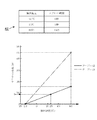
図4の上段は、テーブル42の一例を示している。温度センサ41による検出温度が−20℃、25℃、60℃であるときに夫々オフセット時間を0秒、9秒、15秒として設定している。ここでは後述の評価試験の試験結果に基づいてオフセット時間を設定している。前記検出温度が−20℃〜25℃の間及び25℃〜60℃の間であったときは、例えばこれらの温度範囲において夫々検出温度とオフセット時間との間に比例関係があるものとし、前記検出温度及び当該比例関係に基づいてオフセット時間が決定される。言い換えると、図4の下段の実線のグラフから、前記検出温度に対応するオフセット時間を読み出して決定することになる。なお、このグラフの横軸、縦軸は夫々前記検出温度(単位:℃)、オフセット時間(単位:秒)として設定されている。
The upper part of FIG. 4 shows an example of the table 42. When the temperature detected by the
テーブル43では、例えば検出温度が−20℃、60℃であるときにオフセット時間を0秒、45秒として設定している。前記検出温度が−20℃〜60℃の間であるときは、テーブル42を用いる場合と同様、例えばこれらの温度範囲において夫々検出温度とオフセット時間との間に比例関係があるものとし、前記検出温度及び当該比例関係に基づいてオフセット時間が決定される。つまり、図4の下段の鎖線のグラフから、前記検出温度に対応するオフセット時間を読み出して決定することになる。各テーブル42、43の検出温度と、オフセット時間との対応関係については、周波数シンセサイザ1の特性に応じて予め実験を行うことによって、例えば周波数シンセサイザ1の個体ごとに決められる。 In the table 43, for example, when the detected temperature is −20 ° C. and 60 ° C., the offset time is set to 0 seconds and 45 seconds. When the detected temperature is between −20 ° C. and 60 ° C., as in the case of using the table 42, for example, it is assumed that there is a proportional relationship between the detected temperature and the offset time in these temperature ranges. The offset time is determined based on the temperature and the proportional relationship. That is, the offset time corresponding to the detected temperature is read and determined from the chain line graph in the lower part of FIG. The correspondence relationship between the detected temperatures of the tables 42 and 43 and the offset time is determined, for example, for each individual frequency synthesizer 1 by performing an experiment in advance according to the characteristics of the frequency synthesizer 1.
続いて、周波数シンセサイザ1の電源投入時における動作を説明する。先ず、周波数シンセサイザ1のユーザが当該シンセサイザ1の電源を投入すると、OCXO20においてヒータ回路部3のトランジスタ33のコレクタ電流がしきい値以下であるか否かが判断される。ここでは発振回路2が置かれている雰囲気は室温であり、設定温度は当該室温よりも高いものとする。即ち、前記コレクタ電流はしきい値よりも高いと判断される。そして、OCXO20は恒温槽内が設定温度に向けて昇温中であると判断されたことを示すオーブンアラーム信号(論理信号「L」)を、制御回路4に出力する。
Next, an operation when the frequency synthesizer 1 is turned on will be described. First, when the user of the frequency synthesizer 1 turns on the power of the synthesizer 1, it is determined in the
この論理信号の受信に並行して制御回路4は、温度センサ41の出力に基づいてOCXO20が設けられる雰囲気の温度を検出する。さらにこの検出動作に並行して、検波回路16を介して入力された外部基準信号の振幅が許容範囲に収まっているか否かを判定する。ここでは、前記振幅が許容範囲に収まっていると判定されたものとする。
In parallel with the reception of the logic signal, the control circuit 4 detects the temperature of the atmosphere in which the
制御回路4が、PLL−IC11とループフィルタ13とを接続するようにスイッチ12を動作させ、外部基準信号がPLL−IC11及びループフィルタ13を介してOCXO20に入力されて、当該OCXO20が発振する。またOCXO20の出力が、PLL−IC51及びループフィルタ52を介してVCO53に入力されてVCO53も発振し、その発振出力がAMP54で増幅されて上位装置へと出力される。このように出力がなされることに並行して、制御回路4は、前記温度センサ41により検出された温度とテーブル42とに基づいて、オフセット時間を決定する。また、上位装置に対して周波数シンセサイザ1の周波数が安定していないことを示す出力不安定ステータス信号を出力する。
The control circuit 4 operates the
OCXO20、VCO53を含む各PLLがロックされ、そのようにロックされたことを示す信号が制御回路4から上位装置に出力される。また、OCXO20の恒温槽内の温度が上昇して設定温度に近づくと、トランジスタ33のコレクタ電流が下がり始める。そして、前記コレクタ電流がしきい値以下になると(図3中t)、OCXO20において恒温槽内の昇温が完了したと判断されて、OCXO20からオーブンアラーム信号に代わりオーブンアラーム解除信号(論理信号「H」)が出力される。
Each PLL including the
制御回路4は、オーブンアラーム解除信号を受信した後、決定したオフセット時間待機する。この待機している間にOCXO20からの出力は安定し、それによって周波数シンセサイザ1から上位装置への出力も安定する。そして、前記オーブンアラーム信号を受信してからオフセット時間が経過すると、制御回路4は当該周波数シンセサイザ1の周波数が安定したものとして、出力不安定ステータス信号に代わり出力安定ステータス信号を出力する。この出力安定ステータス信号を受信することによって、上位装置は、周波数シンセサイザ1からの出力を用いて、その運用が開始される。なお、このステータス信号が出力されたときに、例えば既に電源が投入されている上位装置が自動的にシンセサイザ1の周波数を用いるように動作するように構成されていてもよいし、前記ステータス信号が出力されたときに、上位装置の電源が投入されて上位装置の運用が開始されるようにしても良い。また、前記ステータス信号が出力されたときに、ユーザが当該上位装置の電源を投入するようにしてもよい。
The control circuit 4 waits for the determined offset time after receiving the oven alarm release signal. During this waiting time, the output from the
検波された外部基準信号の振幅が許容範囲外と判定された場合について、許容範囲内と判定された場合との差異点を中心に述べる。このように許容範囲外と判定されたときには、制御回路4は、固定電圧供給端子14とループフィルタ13とが接続されるようにスイッチ12を動作させる。固定電圧信号がループフィルタ13を介してOCXO20に供給されて当該OCXO20が発振し、それによってVCO53も発振する。制御回路4は、温度センサ41により検出された温度と、テーブル43とに基づいて、オフセット時間を決定する。以降は、外部基準信号が入力された場合と同様に、オーブンアラーム解除信号が出力された時点から前記オフセット時間が経過すると、出力安定ステータス信号が出力される。
The difference between the case where the amplitude of the detected external reference signal is determined to be outside the allowable range and the case where the amplitude is determined to be within the allowable range will be mainly described. Thus, when it is determined that the value is outside the allowable range, the control circuit 4 operates the
この周波数シンセサイザ1によれば、電源投入後、ヒータ回路部3によりOCXO20の恒温槽内の雰囲気の温度が設定温度になったことを示すオーブンアラーム解除信号が制御回路4に出力された後、電源投入時に温度センサ41により検出されるOCXO20の周囲の雰囲気の温度と、テーブル42または43とに基づいて決定したオフセット時間が経過した後に、制御回路4が上位装置に対して周波数シンセサイザ1の出力周波数が安定したことを示す出力安定ステータス信号を出力する。従って、実際にOCXO20の出力周波数、ひいては前記周波数シンセサイザ1の出力周波数が安定してから、前記出力安定ステータス信号が出力されるまでの時間のずれを抑えることができる。従って、周波数シンセサイザ1の出力を利用する上位装置の動作が不安定になることを抑え、且つ当該上位装置の運用効率を高くすることができる。さらに、OCXO20を動作させるために周波数シンセサイザ1に入力される入力信号に応じて、テーブル42、43のうち適切なテーブルのデータが使用されるため、前記時間のずれをより確実に抑えることができる。
According to the frequency synthesizer 1, after the power is turned on, the
周波数が安定することを、例えば周波数偏差が−0.1ppm〜+0.1ppmの範囲に収束するとしたが、この周波数偏差の値は、装置に要求される性能によって異なる。例えば、周波数偏差が−1ppm〜+1ppmの範囲に収束したり、−0.01ppm〜+0.01ppmの範囲に収束したときに周波数が安定しているものとして、前記オフセット時間を設定してもよい。また、OCXO20の発熱により当該OCXO20が設けられる雰囲気の温度が変化するため、温度センサ41により前記雰囲気の温度を検出するのは、電源投入時とする。ただし、ヒータ回路部3の性能によっては電源投入後、昇温するまでに長い時間がかかる場合がある。即ち、電源投入時とは、電源を投入した瞬間だけを指すのではなく、当該瞬間から実質的に温度センサ41による検出温度が変化しない期間も含まれる。例えば、電源投入直後に、温度センサ41による温度検出値が当該電源投入直後から1℃上昇するまでの期間も電源投入時に含まれる。
For example, the frequency deviation is converged to a range of −0.1 ppm to +0.1 ppm, and the value of the frequency deviation varies depending on performance required for the apparatus. For example, the offset time may be set on the assumption that the frequency is stable when the frequency deviation converges to a range of -1 ppm to +1 ppm or when the frequency deviation converges to a range of -0.01 ppm to +0.01 ppm. Further, since the temperature of the atmosphere in which the
ところで、OCXO20の温度に対する周波数特性は、水晶振動子21の温度に対する周波数特性に依存するので、オフセット時間を決定するために温度センサにより検出される温度は、水晶振動子21により近い雰囲気の温度であることが好ましい。即ち、上記の例では電源投入時には恒温槽の内外は同様の温度であるものとして、温度センサ41により恒温槽の外部の温度を検出しているが、そのようにする代わりに、温度センサ41を恒温槽の内部に設けて恒温槽の内部の温度を検出するようにしてもよい。それによって、より確実に前記出力安定ステータス信号を出力するタイミングと、実際に出力周波数が安定するタイミングとのずれを抑えることができる。また、前記ヒータ回路部3のサーミスタ31が、温度センサ41の役割を有するようにしてもよい。つまり、例えば電源投入時のトランジスタ33のコレクタ電流に基づいて、制御回路4が恒温槽内の温度を検出できるようにしてもよい。
By the way, since the frequency characteristic with respect to the temperature of the
上記の例では外部基準信号の異常の有無について振幅を検出することにより判定してスイッチ12の切り替えを行っているが、このような構成に限られない。例えば外部基準信号の電圧を検出し、その検出電圧に基づいて異常の有無を判定し、スイッチ12の切り替えを行ってもよい。
In the above example, whether or not the external reference signal is abnormal is determined by detecting the amplitude, and the
(評価試験1)
ここで、本発明の知見を得るに至った評価試験について説明する。この評価試験では、試験用の周波数シンセサイザを用いた。この試験用の周波数シンセサイザにおいては、テーブル42、43及び温度センサ41が設けられていない。そして、OCXO20からオーブンアラーム解除信号が出力されると、制御回路4は、周波数シンセサイザ1の発振周波数が安定したものとして速やかにステータス信号を出力する。そのような差異を除いて、試験用の周波数シンセサイザは周波数シンセサイザ1と同様に構成されている。
(Evaluation Test 1)
Here, the evaluation test that has resulted in the knowledge of the present invention will be described. In this evaluation test, a test frequency synthesizer was used. In the test frequency synthesizer, the tables 42 and 43 and the
評価試験1−1として、試験用の周波数シンセサイザを−20℃の雰囲気に設置し、電源を投入した。そして、電源投入からオーブンアラーム解除信号が出力されるまでの時間(オーブンアラーム解除時間とする)を測定した。また、周波数偏差をモニタし、この周波数偏差が電源投入後から−0.1ppm〜+0.1ppmとなるまでの時間を測定した。評価試験1−2として、試験用の周波数シンセサイザを25℃の雰囲気に設置した他は評価試験1−1と同様に試験を行った。評価試験1−3として、試験用の周波数シンセサイザを60℃の雰囲気に設置した他は評価試験1−1と同様に試験を行った。これら評価試験1−1〜1−3では、試験用の周波数シンセサイザを外部基準信号に同期させた。 As evaluation test 1-1, a test frequency synthesizer was installed in an atmosphere of −20 ° C., and the power was turned on. Then, the time from when the power was turned on until the oven alarm release signal was output (the oven alarm release time) was measured. Further, the frequency deviation was monitored, and the time until the frequency deviation became −0.1 ppm to +0.1 ppm after the power was turned on was measured. As evaluation test 1-2, a test was performed in the same manner as evaluation test 1-1 except that a test frequency synthesizer was installed in an atmosphere of 25 ° C. As evaluation test 1-3, a test was performed in the same manner as evaluation test 1-1 except that a test frequency synthesizer was installed in an atmosphere of 60 ° C. In these evaluation tests 1-1 to 1-3, the test frequency synthesizer was synchronized with the external reference signal.
図5は、モニタした周波数偏差(単位:ppm)と、電源投入時からの経過時間(単位:秒)との関係を示したグラフであり、横軸、縦軸に夫々経過時間、周波数偏差を夫々設定している。評価試験1−1、1−2、1−3の結果を鎖線、点線、実線で夫々示している。評価試験1−1〜1−3の全てにおいて、グラフに示すように、時間が経過するにつれて発振周波数は安定している。 FIG. 5 is a graph showing the relationship between the monitored frequency deviation (unit: ppm) and the elapsed time since the power was turned on (unit: seconds). The horizontal axis and the vertical axis show the elapsed time and frequency deviation, respectively. Each is set. The results of evaluation tests 1-1, 1-2, and 1-3 are shown by chain lines, dotted lines, and solid lines, respectively. In all of the evaluation tests 1-1 to 1-3, as shown in the graph, the oscillation frequency is stable as time elapses.
図6は、図5のグラフにおいて周波数偏差が−1.0ppm〜+1.0ppmである範囲を拡大して示している。この図6のグラフ中にて、オーブンアラーム解除信号が出力された時点を白丸のプロットで示している。また、周波数偏差が−0.1ppm〜+0.1ppmに収束した時点を黒丸のプロットで示している。評価試験1−1、1−2、1−3において、前記オーブンアラーム解除時間は夫々170秒、75秒、23秒であり、オーブンアラーム解除信号が出力されたときの周波数偏差は夫々0.04ppm、-0.01ppm、-0.09ppmであった。また、評価試験1−1、1−2、1−3において、電源投入時から周波数偏差が−0.1ppm〜+0.1ppmに収束するまでの時間(収束時間)は、夫々161秒、84秒、38秒であった。 FIG. 6 shows an enlarged range in which the frequency deviation is −1.0 ppm to +1.0 ppm in the graph of FIG. 5. In the graph of FIG. 6, the time point when the oven alarm cancel signal is output is indicated by a white circle. In addition, the time points when the frequency deviation converges to −0.1 ppm to +0.1 ppm are indicated by black circle plots. In the evaluation tests 1-1, 1-2, and 1-3, the oven alarm release time is 170 seconds, 75 seconds, and 23 seconds, respectively, and the frequency deviation when the oven alarm release signal is output is 0.04 ppm, respectively. -0.01 ppm and -0.09 ppm. In evaluation tests 1-1, 1-2, and 1-3, the time from when the power is turned on until the frequency deviation converges to −0.1 ppm to +0.1 ppm (convergence time) is 161 seconds and 84 seconds, respectively. It was 38 seconds.
従って評価試験1−1、1−2、1−3において、前記収束時間−オーブンアラーム解除時間を計算すると、夫々−9秒、9秒、15秒である。即ち、この時間差に相当する分をオーブンアラーム解除信号が出力されてからのオフセットとして、前記出力安定ステータス信号が出力されるタイミングを制御することで、周波数シンセサイザ1の出力周波数が安定してから、出力安定ステータス信号が出力されるまでの時間のずれを抑えることができることになる。 Therefore, in the evaluation tests 1-1, 1-2, and 1-3, the convergence time-oven alarm release time is calculated to be -9 seconds, 9 seconds, and 15 seconds, respectively. That is, the amount corresponding to this time difference is set as an offset from the output of the oven alarm release signal, and the timing at which the output stability status signal is output is controlled to stabilize the output frequency of the frequency synthesizer 1, A time lag until the output stable status signal is output can be suppressed.
周波数シンセサイザ1のテーブル42のオフセット時間は、この評価試験1−1〜1−3に基づいて設定している。評価試験1−3において前記収束時間とオーブンアラーム解除時間との時間差は−9秒であるが、制御回路4はOCXO20からオーブンアラーム解除信号を受信してから、前記ステータス信号を出力するため、テーブル42において温度センサ41の検出温度が−20℃であるときのオフセット時間は0秒に設定している。ただし、より確実に周波数が安定した状態で上位装置を運用するために、このように実験を行ってオフセット時間を決定する場合、前記収束時間−オーブンアラーム解除時間よりも若干長い時間をオフセット時間とすることも有効である。
The offset time of the table 42 of the frequency synthesizer 1 is set based on the evaluation tests 1-1 to 1-3. In evaluation test 1-3, the time difference between the convergence time and the oven alarm release time is −9 seconds, but the control circuit 4 receives the oven alarm release signal from the
(評価試験2)
評価試験2−1として、上記の試験用の周波数シンセサイザを60℃の雰囲気に設置し、電源投入後の周波数偏差をモニタした。この評価試験2−1では外部基準信号に前記周波数シンセサイザを同期させた。また、外部基準信号を用いる代わりに固定電圧信号を用いて評価試験2−2を行った。この評価試験2−2では、そのように入力信号が異なる他は、評価試験2−1と同様の条件で実験を行った。
(Evaluation test 2)
As the evaluation test 2-1, the frequency synthesizer for the above test was installed in an atmosphere of 60 ° C., and the frequency deviation after power-on was monitored. In this evaluation test 2-1, the frequency synthesizer was synchronized with an external reference signal. Also, evaluation test 2-2 was performed using a fixed voltage signal instead of using an external reference signal. In this evaluation test 2-2, an experiment was performed under the same conditions as in the evaluation test 2-1, except that the input signal was different.
図7は、評価試験2−1、2−2の結果を示すグラフであり、図5、図6のグラフと同様に、横軸に電源投入時からの経過時間、縦軸に周波数偏差を夫々設定している。評価試験2−1の結果を点線のグラフで、評価試験2−2の結果を実線のグラフで夫々示している。OCXO20の周波数の可変範囲は例えば−2ppm〜+2ppmであり、評価試験2−1では電源投入後、速やかにOCXO20は外部基準信号に同期できることがグラフから分かる。そして、評価試験2−1においては、オーバーシュートもなく、周波数が安定するまでに要する時間は評価試験2−2よりも短い。この評価試験2−1、2−2から、上記の周波数シンセサイザ1のように外部基準信号の供給の有無に従って、テーブル42、43のうちの一方を選択してオフセット時間を決定することが有効であることが分かる。
FIG. 7 is a graph showing the results of the evaluation tests 2-1 and 2-2. Like the graphs of FIGS. 5 and 6, the horizontal axis represents the elapsed time since power-on, and the vertical axis represents the frequency deviation. It is set. The result of the evaluation test 2-1 is indicated by a dotted line graph, and the result of the evaluation test 2-2 is indicated by a solid line graph. The variable range of the frequency of the
続いて、周波数シンセサイザ6について図8を参照しながら説明する。この周波数シンセサイザ6は、n個(nは整数)の信号生成部60を含む。各信号生成部60は互いに同様に構成され、PLL−IC61、フィルタ62、VCO63、減衰器64、増幅器65、及びフィルタ66がこの順に接続されて構成される。図8では、信号生成部60を互いに区別して示すために、便宜上信号生成部60の数字の後に1〜nの符号を付して示し、信号生成部601、602・・・60nとして示している。そして、これら信号生成部601〜60nを構成する上記の各部についても同様に、61〜66の数字の後に信号生成部に付した1〜nの符号を付して示し、信号生成部601、602・・・60nのいずれを構成しているかを示している。
Next, the
VCO63の出力はPLL−IC61に帰還される。それによって、PLL−IC61、フィルタ62及びVCO63はPLLを構成している。各信号生成部601、602・・・60nは互いに異なる帯域の周波数を出力できるように構成され、これら信号生成部601、602・・・60nのフィルタ661、662・・・66nは出力帯域選択部67に接続されている。この出力帯域選択部67により、信号生成部601、602・・・60nのうちのいずれか一つの出力が出力端子68に供給される。また、周波数シンセサイザ6は、制御部71及び電源部72を備えている。制御部71は、制御回路4と同様に各PLL−ICにデータを出力する。また、前記出力帯域選択部67を制御し、どの信号生成部60のデータを出力するかを決定する。電源部72は、周波数シンセサイザ6の各部に電力を供給する。
The output of the VCO 63 is fed back to the PLL-IC 61. Thereby, the PLL-IC 61, the filter 62, and the VCO 63 constitute a PLL. Each of the
図9に示すように、周波数シンセサイザ6は、既述の信号生成部60、帯域選択部67、制御部71及び電源部72を構成する回路部品73が、基板74上に配置されて構成される。この基板74上にケース75が設けられ、このケース75は、厚板の下面に複数の凹部が形成されて構成される。この凹部に前記回路部品73が収納される。ケース75において、このように1つの凹部を形成し、回路部品73の側周を囲む側壁81及び回路部品73の上側を覆う上壁82をシールドブロック7と記載する。つまり、ケース75には複数のシールドブロック7が形成され、各回路部品73は、各シールドブロック7により区画されている。
As shown in FIG. 9, the
例えば前記図8には、1つの点線の枠で1つのシールドブロック7に含まれる周波数シンセサイザ6の構成要素を示している。この例では各信号生成部60は、互いに異なるシールドブロック7に収納されている。また、信号生成部60において、PLL−IC61、フィルタ62及びVCO63が一つのシールドブロック7に、減衰器64、増幅器65及びフィルタ66が他のシールドブロック7に収納されている。制御部71、電源部72、出力帯域選択部67は互いに独立したシールドブロック7に収納されている。
For example, FIG. 8 shows the components of the
基板74と側壁81との間には、当該側壁81に沿って導電性のガスケット83が設けられる。シールドブロック7内に各回路部品73が収納されることで、一のシールドブロック7に格納される回路部品73のノイズが、他のシールドブロック7に格納される回路部品73に影響し、スプリアスが発生することを防ぐことができる。さらに、前記ガスケット83を設けることにより、このようなノイズの他のブロック7への影響をより確実に抑えることができる。ケース75の構造上、基板74とケース75との接触性が低く、回路部品73の密閉性が低い場合であっても、このようにガスケット83を設けることで密閉性を高くすることができる。また、ガスケット83としては熱伝導性が比較的高いものを用い、前記シールドブロック7内の放熱性を高めてもよい。図中84は、側壁81の下端部に設けられた孔であり、基板74に対してケース75をネジ止めするために用いられる。
A
上記のシールドブロック7を設けて、各回路部品73を区画することにより、各シールドブロック7内で発生した不要なノイズが他のブロック7の信号に結合することが抑えられる。特に、特開2007-267375号公報に記載されるように、発振装置において制御電圧が印加される制御端子にノイズが印加されると、スプリアスが発生しやすいが、このようなノイズの印加が抑えられることにより、各信号生成部60で夫々不要波が発生することが抑えられる。結果として、周波数シンセサイザ6からの出力周波数が安定する。
By providing the
図10にはシールドブロック7の他の例を示しており、このシールドブロック7の側壁81の下端部には段差が設けられている。この段差によって、側壁81には低壁81Aと、高壁81Bとが形成される。高壁81Bには前記孔84が設けられ、低壁81Aには前記ガスケット83が設けられる。シールドブロック7を基板74に取り付けるときには、ガスケット83が基板74により押し潰され、高壁81Bは基板74に接触することができ、上記のように高壁81Bをネジ止めすることができる。つまり、側壁81に段差を設けることにより、ガスケット83の厚さによって当該側壁81が基板74から浮き上がることを防ぐことができる。
FIG. 10 shows another example of the
シールドブロック7については、他の発振装置にも適用することができる。例えば上記の周波数シンセサイザ1に適用してもよい。具体的には、例えばOCXO20とVCO53とを別々のシールドブロック7に収納してお互いの出力が干渉することを防ぐことができる。さらに、前記特開2007-267375号公報の発振装置にシールドブロック7を適用してもよい。
The
1 周波数シンセサイザ
2 発振回路
20 OCXO
21 水晶振動子
3 ヒータ回路部
14 固定電圧供給端子
4 制御回路
41 温度センサ
42、43 テーブル
1 Frequency synthesizer 2
21
Claims (3)
前記圧電振動子が設けられる雰囲気の温度を設定温度に維持するためのヒータと、
前記雰囲気の温度を検出して当該検出温度に対応する信号を出力する温度センサと、
電源投入後、前記温度センサから前記ヒータにより前記雰囲気の温度が前記設定温度になったことを示す第1の検出信号を受信した後、前記発振回路から出力される発振周波数が安定したことを外部に報知する制御回路と、
電源投入時に前記温度センサから前記制御回路に出力される第2の検出信号と、前記制御回路が前記第1の検出信号を受信してから前記報知を行うまでの遅延時間との対応関係について、前記制御回路が当該対応関係に基づいて前記報知を行うことができるように記憶する記憶部と、
を備えたことを特徴とする発振装置。 An oscillation circuit using a piezoelectric vibrator;
A heater for maintaining the temperature of the atmosphere in which the piezoelectric vibrator is provided at a set temperature;
A temperature sensor that detects the temperature of the atmosphere and outputs a signal corresponding to the detected temperature;
After turning on the power, after receiving a first detection signal indicating that the temperature of the atmosphere has reached the set temperature by the heater from the temperature sensor, it is confirmed that the oscillation frequency output from the oscillation circuit has become stable. A control circuit for informing,
Regarding the correspondence between the second detection signal output from the temperature sensor to the control circuit when the power is turned on and the delay time from when the control circuit receives the first detection signal until the notification is performed, A storage unit that stores the control circuit so that the notification can be performed based on the correspondence;
An oscillation device comprising:
前記基準信号の異常の有無を検出するための検出部と、
を備え、
前記制御回路は、前記検出部の検出結果に従って、切り替え部の動作を制御することを特徴とする請求項1記載の発振装置。 A switching unit for switching a control signal output to the oscillation circuit between a reference signal and a spare signal for replacement of the reference signal;
A detection unit for detecting the presence or absence of abnormality of the reference signal;
With
The oscillation device according to claim 1, wherein the control circuit controls an operation of the switching unit according to a detection result of the detection unit.
前記制御回路は、前記基準信号が前記発振回路に供給されるときに前記第1の対応関係に基づいて前記報知信号を出力し、前記予備信号が前記発振回路に供給されるときに前記第2の対応関係に基づいて前記報知信号を出力することを特徴とする請求項2記載の発振装置。 The correspondence relationship includes a first correspondence relationship and a second correspondence relationship different from each other,
The control circuit outputs the notification signal based on the first correspondence when the reference signal is supplied to the oscillation circuit, and the second signal when the preliminary signal is supplied to the oscillation circuit. The oscillation device according to claim 2, wherein the notification signal is output based on the correspondence relationship.
Priority Applications (1)
| Application Number | Priority Date | Filing Date | Title |
|---|---|---|---|
| JP2013064280A JP6172989B2 (en) | 2013-03-26 | 2013-03-26 | Oscillator |
Applications Claiming Priority (1)
| Application Number | Priority Date | Filing Date | Title |
|---|---|---|---|
| JP2013064280A JP6172989B2 (en) | 2013-03-26 | 2013-03-26 | Oscillator |
Publications (2)
| Publication Number | Publication Date |
|---|---|
| JP2014192578A true JP2014192578A (en) | 2014-10-06 |
| JP6172989B2 JP6172989B2 (en) | 2017-08-02 |
Family
ID=51838509
Family Applications (1)
| Application Number | Title | Priority Date | Filing Date |
|---|---|---|---|
| JP2013064280A Active JP6172989B2 (en) | 2013-03-26 | 2013-03-26 | Oscillator |
Country Status (1)
| Country | Link |
|---|---|
| JP (1) | JP6172989B2 (en) |
Cited By (2)
| Publication number | Priority date | Publication date | Assignee | Title |
|---|---|---|---|---|
| CN109474272A (en) * | 2017-09-07 | 2019-03-15 | 江汉大学 | A kind of temporal frequency signal source with synchronization signal output |
| US10374613B2 (en) | 2016-03-25 | 2019-08-06 | Seiko Epson Corporation | Oscillator, electronic apparatus, and vehicle |
Citations (4)
| Publication number | Priority date | Publication date | Assignee | Title |
|---|---|---|---|---|
| JPH0541675A (en) * | 1990-10-31 | 1993-02-19 | Nec Corp | Radio transmitter-receiver |
| JP2006191327A (en) * | 2005-01-05 | 2006-07-20 | Epson Toyocom Corp | Thin high stable piezoelectric oscillator |
| JP2007189471A (en) * | 2006-01-13 | 2007-07-26 | Nec Saitama Ltd | Warmup method of quartz resonator with thermostatic chamber of mobile communication base station device, and mobile communication base station device |
| JP2009159013A (en) * | 2007-12-25 | 2009-07-16 | Nippon Dempa Kogyo Co Ltd | Oscillation frequency control circuit |
-
2013
- 2013-03-26 JP JP2013064280A patent/JP6172989B2/en active Active
Patent Citations (4)
| Publication number | Priority date | Publication date | Assignee | Title |
|---|---|---|---|---|
| JPH0541675A (en) * | 1990-10-31 | 1993-02-19 | Nec Corp | Radio transmitter-receiver |
| JP2006191327A (en) * | 2005-01-05 | 2006-07-20 | Epson Toyocom Corp | Thin high stable piezoelectric oscillator |
| JP2007189471A (en) * | 2006-01-13 | 2007-07-26 | Nec Saitama Ltd | Warmup method of quartz resonator with thermostatic chamber of mobile communication base station device, and mobile communication base station device |
| JP2009159013A (en) * | 2007-12-25 | 2009-07-16 | Nippon Dempa Kogyo Co Ltd | Oscillation frequency control circuit |
Cited By (2)
| Publication number | Priority date | Publication date | Assignee | Title |
|---|---|---|---|---|
| US10374613B2 (en) | 2016-03-25 | 2019-08-06 | Seiko Epson Corporation | Oscillator, electronic apparatus, and vehicle |
| CN109474272A (en) * | 2017-09-07 | 2019-03-15 | 江汉大学 | A kind of temporal frequency signal source with synchronization signal output |
Also Published As
| Publication number | Publication date |
|---|---|
| JP6172989B2 (en) | 2017-08-02 |
Similar Documents
| Publication | Publication Date | Title |
|---|---|---|
| JP5086479B2 (en) | Oscillator | |
| US20130127551A1 (en) | Crystal reference oscillator for navigation applications | |
| US8653901B2 (en) | Oscillator and control circuit thereof | |
| US11513010B2 (en) | Temperature monitoring | |
| US20140210563A1 (en) | Crystal controlled oscillator and oscillating device | |
| JP2015046704A (en) | Crystal oscillator | |
| JP6548411B2 (en) | Oscillator | |
| JP2008160677A (en) | Oscillation frequency control circuit | |
| JP6172989B2 (en) | Oscillator | |
| JP2008311884A (en) | Oscillation frequency control method, and oscillator | |
| JP5970275B2 (en) | High stability oscillator | |
| JP2015089084A (en) | Oscillator | |
| US9281822B2 (en) | Oscillator | |
| JP5040864B2 (en) | Electronics | |
| JP2008258710A (en) | Temperature compensation piezoelectric oscillator, and temperature compensating method thereof | |
| JP2009290379A (en) | Oscillator | |
| US20150054590A1 (en) | Oven controlled crystal oscillator | |
| JP6286962B2 (en) | Output signal generator | |
| JP2021136642A (en) | Oscillator | |
| JP2011035487A (en) | Oscillator device | |
| JP2001257531A (en) | Crystal oscillator | |
| JP5117823B2 (en) | Highly stable oscillator with temperature chamber | |
| JP5213845B2 (en) | Temperature compensated crystal oscillator | |
| JP2013058898A (en) | Oscillation device | |
| JP2015126249A (en) | Oscillation device |
Legal Events
| Date | Code | Title | Description |
|---|---|---|---|
| A621 | Written request for application examination |
Free format text: JAPANESE INTERMEDIATE CODE: A621 Effective date: 20160113 |
|
| A977 | Report on retrieval |
Free format text: JAPANESE INTERMEDIATE CODE: A971007 Effective date: 20161031 |
|
| A131 | Notification of reasons for refusal |
Free format text: JAPANESE INTERMEDIATE CODE: A131 Effective date: 20161129 |
|
| A521 | Request for written amendment filed |
Free format text: JAPANESE INTERMEDIATE CODE: A523 Effective date: 20170110 |
|
| TRDD | Decision of grant or rejection written | ||
| A01 | Written decision to grant a patent or to grant a registration (utility model) |
Free format text: JAPANESE INTERMEDIATE CODE: A01 Effective date: 20170606 |
|
| A61 | First payment of annual fees (during grant procedure) |
Free format text: JAPANESE INTERMEDIATE CODE: A61 Effective date: 20170704 |
|
| R150 | Certificate of patent or registration of utility model |
Ref document number: 6172989 Country of ref document: JP Free format text: JAPANESE INTERMEDIATE CODE: R150 |
|
| R250 | Receipt of annual fees |
Free format text: JAPANESE INTERMEDIATE CODE: R250 |
|
| R250 | Receipt of annual fees |
Free format text: JAPANESE INTERMEDIATE CODE: R250 |
|
| R250 | Receipt of annual fees |
Free format text: JAPANESE INTERMEDIATE CODE: R250 |
|
| R250 | Receipt of annual fees |
Free format text: JAPANESE INTERMEDIATE CODE: R250 |
|
| R250 | Receipt of annual fees |
Free format text: JAPANESE INTERMEDIATE CODE: R250 |