JP2014190894A - Infrared sensor - Google Patents
Infrared sensor Download PDFInfo
- Publication number
- JP2014190894A JP2014190894A JP2013067855A JP2013067855A JP2014190894A JP 2014190894 A JP2014190894 A JP 2014190894A JP 2013067855 A JP2013067855 A JP 2013067855A JP 2013067855 A JP2013067855 A JP 2013067855A JP 2014190894 A JP2014190894 A JP 2014190894A
- Authority
- JP
- Japan
- Prior art keywords
- absorption
- film
- layer
- absorption film
- infrared
- Prior art date
- Legal status (The legal status is an assumption and is not a legal conclusion. Google has not performed a legal analysis and makes no representation as to the accuracy of the status listed.)
- Granted
Links
- 238000010521 absorption reaction Methods 0.000 claims abstract description 318
- 239000010410 layer Substances 0.000 claims abstract description 145
- 239000011241 protective layer Substances 0.000 claims abstract description 67
- 239000000463 material Substances 0.000 claims abstract description 50
- 239000000758 substrate Substances 0.000 claims abstract description 49
- 239000012528 membrane Substances 0.000 claims abstract description 42
- 239000011368 organic material Substances 0.000 claims abstract description 35
- 230000005540 biological transmission Effects 0.000 claims description 12
- 238000006243 chemical reaction Methods 0.000 claims description 5
- 238000004132 cross linking Methods 0.000 claims description 3
- 206010034972 Photosensitivity reaction Diseases 0.000 claims 2
- 230000036211 photosensitivity Effects 0.000 claims 2
- 230000035945 sensitivity Effects 0.000 abstract description 13
- 230000006866 deterioration Effects 0.000 abstract description 5
- 239000011248 coating agent Substances 0.000 abstract 1
- 238000000576 coating method Methods 0.000 abstract 1
- 238000003475 lamination Methods 0.000 abstract 1
- 239000010408 film Substances 0.000 description 295
- 238000000034 method Methods 0.000 description 56
- 239000010409 thin film Substances 0.000 description 43
- 230000008569 process Effects 0.000 description 42
- 238000000605 extraction Methods 0.000 description 35
- 230000000694 effects Effects 0.000 description 31
- 230000000052 comparative effect Effects 0.000 description 25
- 238000001514 detection method Methods 0.000 description 16
- 238000005033 Fourier transform infrared spectroscopy Methods 0.000 description 15
- 229910052751 metal Inorganic materials 0.000 description 14
- 239000002184 metal Substances 0.000 description 14
- 238000000206 photolithography Methods 0.000 description 14
- 230000001681 protective effect Effects 0.000 description 14
- VYPSYNLAJGMNEJ-UHFFFAOYSA-N Silicium dioxide Chemical compound O=[Si]=O VYPSYNLAJGMNEJ-UHFFFAOYSA-N 0.000 description 13
- BASFCYQUMIYNBI-UHFFFAOYSA-N platinum Chemical compound [Pt] BASFCYQUMIYNBI-UHFFFAOYSA-N 0.000 description 12
- 230000004044 response Effects 0.000 description 11
- 238000002834 transmittance Methods 0.000 description 11
- 230000015572 biosynthetic process Effects 0.000 description 10
- 230000007423 decrease Effects 0.000 description 9
- 239000010931 gold Substances 0.000 description 8
- 238000005530 etching Methods 0.000 description 7
- 239000007789 gas Substances 0.000 description 7
- 239000004642 Polyimide Substances 0.000 description 6
- 230000002745 absorbent Effects 0.000 description 6
- 239000002250 absorbent Substances 0.000 description 6
- PCHJSUWPFVWCPO-UHFFFAOYSA-N gold Chemical compound [Au] PCHJSUWPFVWCPO-UHFFFAOYSA-N 0.000 description 6
- 229910052737 gold Inorganic materials 0.000 description 6
- 238000001020 plasma etching Methods 0.000 description 6
- 229920001721 polyimide Polymers 0.000 description 6
- 235000012239 silicon dioxide Nutrition 0.000 description 6
- 239000000377 silicon dioxide Substances 0.000 description 6
- 239000000126 substance Substances 0.000 description 6
- 230000008859 change Effects 0.000 description 5
- 230000007613 environmental effect Effects 0.000 description 5
- 238000004544 sputter deposition Methods 0.000 description 5
- 238000004519 manufacturing process Methods 0.000 description 4
- 238000000059 patterning Methods 0.000 description 4
- 229910052697 platinum Inorganic materials 0.000 description 4
- 238000002310 reflectometry Methods 0.000 description 4
- 229920002050 silicone resin Polymers 0.000 description 4
- 239000010936 titanium Substances 0.000 description 4
- OKTJSMMVPCPJKN-UHFFFAOYSA-N Carbon Chemical compound [C] OKTJSMMVPCPJKN-UHFFFAOYSA-N 0.000 description 3
- KDLHZDBZIXYQEI-UHFFFAOYSA-N Palladium Chemical compound [Pd] KDLHZDBZIXYQEI-UHFFFAOYSA-N 0.000 description 3
- 229910052799 carbon Inorganic materials 0.000 description 3
- 238000010586 diagram Methods 0.000 description 3
- 238000001312 dry etching Methods 0.000 description 3
- 230000005611 electricity Effects 0.000 description 3
- 239000000945 filler Substances 0.000 description 3
- 238000005259 measurement Methods 0.000 description 3
- 239000007769 metal material Substances 0.000 description 3
- 230000035699 permeability Effects 0.000 description 3
- 229920005989 resin Polymers 0.000 description 3
- 239000011347 resin Substances 0.000 description 3
- 230000003068 static effect Effects 0.000 description 3
- VXZBYIWNGKSFOJ-UHFFFAOYSA-N 2-[4-[5-(2,3-dihydro-1H-inden-2-ylamino)pyrazin-2-yl]pyrazol-1-yl]-1-(2,4,6,7-tetrahydrotriazolo[4,5-c]pyridin-5-yl)ethanone Chemical compound C1C(CC2=CC=CC=C12)NC=1N=CC(=NC=1)C=1C=NN(C=1)CC(=O)N1CC2=C(CC1)NN=N2 VXZBYIWNGKSFOJ-UHFFFAOYSA-N 0.000 description 2
- 229910020630 Co Ni Inorganic materials 0.000 description 2
- 229910002440 Co–Ni Inorganic materials 0.000 description 2
- XUIMIQQOPSSXEZ-UHFFFAOYSA-N Silicon Chemical compound [Si] XUIMIQQOPSSXEZ-UHFFFAOYSA-N 0.000 description 2
- 229910052782 aluminium Inorganic materials 0.000 description 2
- XAGFODPZIPBFFR-UHFFFAOYSA-N aluminium Chemical compound [Al] XAGFODPZIPBFFR-UHFFFAOYSA-N 0.000 description 2
- QVGXLLKOCUKJST-UHFFFAOYSA-N atomic oxygen Chemical compound [O] QVGXLLKOCUKJST-UHFFFAOYSA-N 0.000 description 2
- 239000002131 composite material Substances 0.000 description 2
- 239000000470 constituent Substances 0.000 description 2
- 239000013078 crystal Substances 0.000 description 2
- 230000003247 decreasing effect Effects 0.000 description 2
- 238000011161 development Methods 0.000 description 2
- 230000006872 improvement Effects 0.000 description 2
- 229910044991 metal oxide Inorganic materials 0.000 description 2
- 150000004706 metal oxides Chemical class 0.000 description 2
- 239000003960 organic solvent Substances 0.000 description 2
- 229910052760 oxygen Inorganic materials 0.000 description 2
- 239000001301 oxygen Substances 0.000 description 2
- 239000011148 porous material Substances 0.000 description 2
- 229910052710 silicon Inorganic materials 0.000 description 2
- 239000010703 silicon Substances 0.000 description 2
- 239000002904 solvent Substances 0.000 description 2
- 230000001629 suppression Effects 0.000 description 2
- 229910052721 tungsten Inorganic materials 0.000 description 2
- 238000001039 wet etching Methods 0.000 description 2
- ZRPAUEVGEGEPFQ-UHFFFAOYSA-N 2-[4-[2-(2,3-dihydro-1H-inden-2-ylamino)pyrimidin-5-yl]pyrazol-1-yl]-1-(2,4,6,7-tetrahydrotriazolo[4,5-c]pyridin-5-yl)ethanone Chemical compound C1C(CC2=CC=CC=C12)NC1=NC=C(C=N1)C=1C=NN(C=1)CC(=O)N1CC2=C(CC1)NN=N2 ZRPAUEVGEGEPFQ-UHFFFAOYSA-N 0.000 description 1
- JVKRKMWZYMKVTQ-UHFFFAOYSA-N 2-[4-[2-(2,3-dihydro-1H-inden-2-ylamino)pyrimidin-5-yl]pyrazol-1-yl]-N-(2-oxo-3H-1,3-benzoxazol-6-yl)acetamide Chemical compound C1C(CC2=CC=CC=C12)NC1=NC=C(C=N1)C=1C=NN(C=1)CC(=O)NC1=CC2=C(NC(O2)=O)C=C1 JVKRKMWZYMKVTQ-UHFFFAOYSA-N 0.000 description 1
- KRHYYFGTRYWZRS-UHFFFAOYSA-M Fluoride anion Chemical compound [F-] KRHYYFGTRYWZRS-UHFFFAOYSA-M 0.000 description 1
- 229910021578 Iron(III) chloride Inorganic materials 0.000 description 1
- ZOKXTWBITQBERF-UHFFFAOYSA-N Molybdenum Chemical compound [Mo] ZOKXTWBITQBERF-UHFFFAOYSA-N 0.000 description 1
- 206010037660 Pyrexia Diseases 0.000 description 1
- 230000005678 Seebeck effect Effects 0.000 description 1
- 229910052581 Si3N4 Inorganic materials 0.000 description 1
- 229910004298 SiO 2 Inorganic materials 0.000 description 1
- BOTDANWDWHJENH-UHFFFAOYSA-N Tetraethyl orthosilicate Chemical compound CCO[Si](OCC)(OCC)OCC BOTDANWDWHJENH-UHFFFAOYSA-N 0.000 description 1
- RTAQQCXQSZGOHL-UHFFFAOYSA-N Titanium Chemical compound [Ti] RTAQQCXQSZGOHL-UHFFFAOYSA-N 0.000 description 1
- 239000000956 alloy Substances 0.000 description 1
- 229910045601 alloy Inorganic materials 0.000 description 1
- 238000000137 annealing Methods 0.000 description 1
- 238000003491 array Methods 0.000 description 1
- 239000012298 atmosphere Substances 0.000 description 1
- 230000008901 benefit Effects 0.000 description 1
- 239000006229 carbon black Substances 0.000 description 1
- 239000000919 ceramic Substances 0.000 description 1
- 238000003486 chemical etching Methods 0.000 description 1
- 239000003795 chemical substances by application Substances 0.000 description 1
- 238000005229 chemical vapour deposition Methods 0.000 description 1
- 230000007797 corrosion Effects 0.000 description 1
- 238000005260 corrosion Methods 0.000 description 1
- 238000000151 deposition Methods 0.000 description 1
- 239000006185 dispersion Substances 0.000 description 1
- 238000006073 displacement reaction Methods 0.000 description 1
- 238000005516 engineering process Methods 0.000 description 1
- 238000011156 evaluation Methods 0.000 description 1
- 230000002349 favourable effect Effects 0.000 description 1
- NBVXSUQYWXRMNV-UHFFFAOYSA-N fluoromethane Chemical compound FC NBVXSUQYWXRMNV-UHFFFAOYSA-N 0.000 description 1
- 239000011521 glass Substances 0.000 description 1
- 230000017525 heat dissipation Effects 0.000 description 1
- 230000020169 heat generation Effects 0.000 description 1
- 238000010438 heat treatment Methods 0.000 description 1
- 229910001385 heavy metal Inorganic materials 0.000 description 1
- 239000011810 insulating material Substances 0.000 description 1
- 238000009413 insulation Methods 0.000 description 1
- 239000012212 insulator Substances 0.000 description 1
- 150000002500 ions Chemical class 0.000 description 1
- 229910052741 iridium Inorganic materials 0.000 description 1
- GKOZUEZYRPOHIO-UHFFFAOYSA-N iridium atom Chemical compound [Ir] GKOZUEZYRPOHIO-UHFFFAOYSA-N 0.000 description 1
- RBTARNINKXHZNM-UHFFFAOYSA-K iron trichloride Chemical compound Cl[Fe](Cl)Cl RBTARNINKXHZNM-UHFFFAOYSA-K 0.000 description 1
- 239000011159 matrix material Substances 0.000 description 1
- 230000008018 melting Effects 0.000 description 1
- 238000002844 melting Methods 0.000 description 1
- 150000002739 metals Chemical class 0.000 description 1
- 239000000203 mixture Substances 0.000 description 1
- 229910052750 molybdenum Inorganic materials 0.000 description 1
- 239000011733 molybdenum Substances 0.000 description 1
- 125000002524 organometallic group Chemical group 0.000 description 1
- 230000003647 oxidation Effects 0.000 description 1
- 238000007254 oxidation reaction Methods 0.000 description 1
- 229910052763 palladium Inorganic materials 0.000 description 1
- 231100000572 poisoning Toxicity 0.000 description 1
- 230000000607 poisoning effect Effects 0.000 description 1
- 229920000642 polymer Polymers 0.000 description 1
- 239000000843 powder Substances 0.000 description 1
- 238000012545 processing Methods 0.000 description 1
- 239000010453 quartz Substances 0.000 description 1
- 230000005855 radiation Effects 0.000 description 1
- 229910052594 sapphire Inorganic materials 0.000 description 1
- 239000010980 sapphire Substances 0.000 description 1
- HQVNEWCFYHHQES-UHFFFAOYSA-N silicon nitride Chemical compound N12[Si]34N5[Si]62N3[Si]51N64 HQVNEWCFYHHQES-UHFFFAOYSA-N 0.000 description 1
- 238000004528 spin coating Methods 0.000 description 1
- 238000000992 sputter etching Methods 0.000 description 1
- 229910052715 tantalum Inorganic materials 0.000 description 1
- GUVRBAGPIYLISA-UHFFFAOYSA-N tantalum atom Chemical compound [Ta] GUVRBAGPIYLISA-UHFFFAOYSA-N 0.000 description 1
- 229910052719 titanium Inorganic materials 0.000 description 1
- 238000012546 transfer Methods 0.000 description 1
- WFKWXMTUELFFGS-UHFFFAOYSA-N tungsten Chemical compound [W] WFKWXMTUELFFGS-UHFFFAOYSA-N 0.000 description 1
- 239000010937 tungsten Substances 0.000 description 1
- 238000007740 vapor deposition Methods 0.000 description 1
- XLYOFNOQVPJJNP-UHFFFAOYSA-N water Substances O XLYOFNOQVPJJNP-UHFFFAOYSA-N 0.000 description 1
Images


Landscapes
- Photometry And Measurement Of Optical Pulse Characteristics (AREA)
- Radiation Pyrometers (AREA)
Abstract
Description
本発明は、赤外線センサに関する。 The present invention relates to an infrared sensor.
赤外線センサは従来より温度センサや、変位を熱量とする様々な応用センサとして開発され、小型で安価なセンサとして使用されている。近年では薄膜、MEMS技術を用いる事により、さらに小型化、高感度化が進んでおり、従来では検知できないほどの微少な熱量を検知できるようになったことによりさらなるアプリケーションの多様化が進み、高速応答のガスセンサや、アレイ化による人感センサなどにも応用されるようになった。 Infrared sensors have been developed as temperature sensors and various applied sensors that use displacement as heat, and are used as small and inexpensive sensors. In recent years, the use of thin film and MEMS technology has led to further miniaturization and higher sensitivity, and since it has become possible to detect minute amounts of heat that cannot be detected in the past, further diversification of applications has progressed. It has come to be applied to response gas sensors and human sensors using arrays.
赤外線を検知し、それを信号に変換しセンシングする手法は、例えばゼーベック効果を使用した、サーモパイルであったり、材料の温度による抵抗変化を使用した、白金抵抗体や、サーミスタなどが上げられる。いずれの方式においても熱容量を極小化することにより赤外線に対する感度が上昇し、非接触にて物質の温度を測定できたり、微小な温度変化を検知することが可能になったが、さらなる感度向上の為には極微小な熱量を拡散させず瞬時に捉えることが必要となり、各高感度赤外線センサにおいては赤外線を吸収する赤外線吸収膜を備えているセンサが多く見られるようになった。 As a method for sensing infrared rays and converting them into signals, for example, a thermopile using the Seebeck effect, or a platinum resistor or thermistor using a resistance change depending on the temperature of the material can be used. In both methods, the sensitivity to infrared rays has increased by minimizing the heat capacity, and it has become possible to measure the temperature of a substance in a non-contact manner and detect minute temperature changes. In order to achieve this, it is necessary to capture a very small amount of heat instantaneously without diffusing, and in each high-sensitivity infrared sensor, many sensors having an infrared absorption film that absorbs infrared rays have been seen.
赤外線吸収膜としては、金黒膜が一般的に知られており、赤外線吸収効率もほぼ100%に近く、材料としては有効であるが、この材料はほぼ粉に近いため吸収膜自体の機械的強度が無く、形成後に容易に壊れる為、メンブレン領域を持つ薄膜型センサにおいては一番強度が弱くなるであろうメンブレン領域に対応するキャビティ形成後に形成せざるを得ず、かつ所望のサイズにパターニングしなければならない為、フォトリソ工程とそのフォトリソを剥離する工程とを通すことにより、肝心のメンブレン領域の構造物が破壊され、歩留りが低下しコスト高になってしまうという問題がある。 As an infrared absorbing film, a gold black film is generally known, and the infrared absorption efficiency is almost 100%, which is effective as a material. However, since this material is almost a powder, the mechanical property of the absorbing film itself Since there is no strength and it breaks easily after formation, a thin film type sensor with a membrane region must be formed after forming a cavity corresponding to the membrane region where the strength will be weakest, and patterning to the desired size Therefore, there is a problem that the structure of the essential membrane region is destroyed by passing through the photolithography process and the process of peeling the photolithography, the yield is lowered, and the cost is increased.
有機膜はそれ自体が赤外線吸収効果をもつ為、有機物を赤外線を吸収膜として利用する方法は有効である。金属黒化膜と比較して軽い為メンブレン領域の構造物の歩留りも向上する。しかし、近年の赤外線センサの様々な用途を考慮すると赤外線吸収膜はセンサ素子の最外層となるため、使用用途に応じた特性や環境耐性も考慮しなければならない。 Since an organic film itself has an infrared absorption effect, a method of using an organic substance as an infrared absorption film is effective. Since it is lighter than the metal blackening film, the yield of structures in the membrane region is improved. However, considering various uses of infrared sensors in recent years, the infrared absorbing film is the outermost layer of the sensor element, and thus characteristics and environmental resistance depending on the use application must be taken into consideration.
有機物吸収膜は赤外線吸収特性向上の為、赤外線を吸収するフィラーを添加し、かつ厚く形成することにより吸収効果を向上させたり、多孔質化による空洞効果を赤外線吸収に利用したりすることで金黒膜と同等の吸収効果を得ることができる。しかし、近年多様化する赤外線センサの用途で、例えば高速応答性が必要になるセンサとして使用したい場合は吸収膜を厚く形成することはメンブレン領域の熱容量の増大を招き、結果応答速度が劣化してしまう。又、多孔質化による空洞効果を利用する場合は吸収膜自体は薄く形成することが可能であるが、例えばガスセンサ等に使用する場合はセンサ素子を気密封止できないため、孔質が被毒化し徐々にセンサ感度が低下する問題が考えられる。 In order to improve the infrared absorption characteristics of the organic substance absorption film, it is possible to improve the absorption effect by adding a filler that absorbs infrared rays and forming it thick, or by utilizing the cavity effect due to the porous structure for infrared absorption. An absorption effect equivalent to that of the black film can be obtained. However, in the application of infrared sensors that have been diversified in recent years, for example, when it is desired to be used as a sensor that requires high-speed response, forming a thick absorption film causes an increase in the heat capacity of the membrane region, resulting in a deterioration in response speed. End up. In addition, when using the cavity effect due to the porous structure, the absorption film itself can be formed thin. However, when used for a gas sensor or the like, for example, the sensor element cannot be hermetically sealed. There may be a problem that the sensor sensitivity gradually decreases.
上記問題を解決する為に、例えば特許3928856号のように無機物である金属多孔質膜を形成する手法がある。多孔質膜はその空洞効果により赤外線吸収効率を高めるため、高効率の赤外線吸収効果をもつ。またこの手法で形成された多孔質膜は無機膜である為、薄膜プロセスの耐性は高く、メンブレン領域に対応するキャビティ形成前に吸収膜構造を形成することが可能である為、メンブレン領域の構造物の歩留り向上も確保でき、結果センサを安価に製造できる利点をもつ。 In order to solve the above problem, there is a method of forming a metal porous film which is an inorganic substance as disclosed in, for example, Japanese Patent No. 3928856. Since the porous film increases the infrared absorption efficiency by the cavity effect, it has a highly efficient infrared absorption effect. In addition, since the porous film formed by this method is an inorganic film, it is highly resistant to thin film processes, and it is possible to form an absorption film structure before forming a cavity corresponding to the membrane area. The improvement in the yield of the object can be ensured, and the resulting sensor can be manufactured at low cost.
又、特開平09−288010号公報の様に孔質SiО2膜、及び有機膜との組み合わせも有効と思われる。孔質シリカや有機膜自体も金黒やカーボンブラックほどではないが、赤外線吸収効果は期待でき、厚く形成することによって十分な赤外線吸収効果が得られる。またこの2つの材料も薄膜プロセス耐性が高い為生産性も十分といえる。
A combination with a
特許文献1では、金属多孔質による赤外線吸収効果を利用している。吸収効果は高いのだが、密度の高い金属材料を使用するため、たとえ多孔質で形成しても、主となるメンブレン領域の構造物に対して重量が重くなる。吸収膜は受光した赤外線熱量を拡散させない為に可能な限りメンブレン領域の内部に形成することが望ましいので重量がある金属多孔質膜を保持する為のメンブレン領域の強度が必要となり、結果メンブレン領域の内部に存在する保護膜の厚みが厚くなり、熱容量が大きくなってしまうという懸念がある。又、ミクロンオーダーの金属膜を表面よりエッチングするには表面濡れ性の影響を大きく受ける為、プロセス過程におけるバラツキが懸念される。エッチング液が吸収膜底面まで浸透しない場合はその底面で赤外線が反射してしまい、プロセス安定性の難易度は比較的高くなってしまうことが懸念される。さらにセンサ素子として考えると金属他孔質膜は素子の最表面に形成されるため、被毒や腐食により、センサの使用環境によっては使用できないという問題がある。 In patent document 1, the infrared absorption effect by a metal porous is utilized. Although the absorption effect is high, since a metal material having a high density is used, even if it is made of a porous material, it is heavier than the main structure of the membrane region. It is desirable that the absorption film be formed inside the membrane region as much as possible in order not to diffuse the received infrared heat, so the strength of the membrane region is necessary to hold the heavy metal porous membrane, and as a result, the membrane region There is a concern that the thickness of the protective film present inside increases and the heat capacity increases. In addition, etching a micron-order metal film from the surface is greatly affected by surface wettability, so there is a concern about variations in the process. If the etching solution does not penetrate to the bottom surface of the absorption film, infrared rays are reflected on the bottom surface, and there is a concern that the difficulty of process stability becomes relatively high. Further, when considered as a sensor element, the metal or other porous film is formed on the outermost surface of the element, so that there is a problem that it cannot be used depending on the sensor use environment due to poisoning or corrosion.
特許文献2では、赤外線を吸収する有機材料を用い、赤外線吸収効果が高いフィラーを添加することによりセンサ感度の向上と共に、プロセス耐性のある材料を選択することでセンサ特性と生産性の向上が見込まれる。しかし、有機材料の赤外線透過特性は材料により異なり、さらには吸収効果の高いフィラー、例えばカーボン等の分散プロセスやフォトリソプロセスも母材となる有機材料により難易度が変化する為、多様化する赤外線センサの環境耐性に対応する為には、それぞれの使用状況下において最適な有機材料と吸収膜形成プロセスを開発しなければならない。さらには有機材料で最も赤外線吸収効果の得られる多孔質化は吸収膜が最外層にあると余分な水分や、環境ガスを吸着してしまう為、好ましくない。
In
上記の問題は最外層に保護層を形成することでも解決できるが保護層自体もセンサ全体の熱容量に寄与してしまう為、例えば赤外線の吸収効果の高い材料を用いたり、保護層をメンブレン領域の外部まで形成してしまうと、保護層で吸収した熱量を感熱膜に伝える前に基板側に逃がしてしまい、結果センサの出力感度が劣化するという問題がある。 The above problem can be solved by forming a protective layer on the outermost layer, but the protective layer itself also contributes to the heat capacity of the entire sensor.For example, a material having a high infrared absorption effect is used, or the protective layer is used in the membrane region. If it is formed to the outside, the amount of heat absorbed by the protective layer escapes to the substrate before it is transmitted to the heat sensitive film, resulting in a problem that the output sensitivity of the sensor deteriorates.
上記の問題点を解決する為、本発明では、高感度を維持し、かつ、赤外線吸収膜の劣化を低減することが可能な赤外線センサを提供することを目的課題とする。 In order to solve the above problems, an object of the present invention is to provide an infrared sensor capable of maintaining high sensitivity and reducing deterioration of the infrared absorption film.
上記目的を達成するために、本発明は、基板と、基板内部に形成されたキャビティと、キャビティに対応したメンブレン領域内に形成された感熱素子の上部に形成された母材が第1の有機材料である吸収膜吸収層と、吸収膜吸収層上に形成されるとともに、吸収膜吸収層を被覆する第2の有機材料である吸収膜保護層とを有し、吸収膜吸収層および吸収膜保護層の積層方向と直交する方向において、吸収膜保護層の端部がメンブレン領域の内部に形成された赤外線センサとする。 In order to achieve the above object, according to the present invention, a substrate, a cavity formed inside the substrate, and a base material formed on an upper part of a thermal element formed in a membrane region corresponding to the cavity are first organic. An absorption film absorption layer that is a material, and an absorption film protection layer that is a second organic material that is formed on the absorption film absorption layer and covers the absorption film absorption layer. In the direction orthogonal to the stacking direction of the protective layer, an infrared sensor in which an end portion of the absorbing film protective layer is formed inside the membrane region is used.
吸収膜吸収層を被覆する第2の有機材料である吸収膜保護層の端部がメンブレン領域の内部に形成されているので、吸収膜吸収層の劣化を低減することが可能であるとともに、吸収膜保護層がメンブレン領域の外部まで存在する場合と比較して高感度とすることが可能である。 Since the end portion of the absorption film protective layer, which is the second organic material covering the absorption film absorption layer, is formed inside the membrane region, it is possible to reduce deterioration of the absorption film absorption layer and absorb The sensitivity can be increased as compared with the case where the membrane protective layer exists outside the membrane region.
本発明は、吸収膜保護層は吸収膜吸収層と同等か、それ以上の赤外線透過特性を有していても良く、吸収膜保護層と吸収膜吸収層との積層構造における赤外線反射特性は、吸収膜保護層および吸収膜吸収層の各々の赤外線反射特性に対し、同等かそれ以下であることとしても良い。 In the present invention, the absorption film protective layer may have an infrared transmission characteristic equal to or higher than that of the absorption film absorption layer, and the infrared reflection characteristic in the laminated structure of the absorption film protection layer and the absorption film absorption layer is: It is good also as being equivalent or less with respect to each infrared reflection characteristic of an absorption film protective layer and an absorption film absorption layer.
本発明は、吸収膜保護層が吸収膜吸収層の形状をトレースする形で形成されていても良い。 In the present invention, the absorption film protective layer may be formed so as to trace the shape of the absorption film absorption layer.
本発明は、第1の有機材料は架橋反応により硬化するとともに、感光性を有する有機材料であっても良い。 In the present invention, the first organic material may be cured by a crosslinking reaction and may be a photosensitive organic material.
本発明は、基板上に形成された感熱素子と、感熱素子の上部に形成された母材が第1の有機材料である吸収膜吸収層と、吸収膜吸収層上に形成されるとともに、吸収膜吸収層を被覆する第2の有機材料である吸収膜保護層とを有し、吸収膜保護層は吸収膜吸収層と同等か、それ以上の赤外線透過特性を有することを特徴とした赤外線センサとしても良い。 The present invention provides a thermal element formed on a substrate, an absorption film absorption layer in which a base material formed on the thermal element is a first organic material, and an absorption film absorption layer. An infrared sensor characterized by having an absorption film protective layer that is a second organic material covering the film absorption layer, and the absorption film protection layer has an infrared transmission characteristic equal to or higher than that of the absorption film absorption layer It is also good.
本発明によれば、高感度を維持し、かつ、赤外線吸収膜の劣化を低減することが可能な赤外線センサを提供することが可能である。 ADVANTAGE OF THE INVENTION According to this invention, it is possible to provide the infrared sensor which can maintain high sensitivity and can reduce deterioration of an infrared rays absorption film.
以下、図面を参照しながら本発明の好適な実施形態について説明する。なお、本発明は以下の実施形態に限定されるものではない。また以下に記載した構成要素には、当業者が容易に想定できるもの、実質的に同一のものが含まれる。さらに以下に記載した構成要素は、適宜組み合わせることができる。 Hereinafter, preferred embodiments of the present invention will be described with reference to the drawings. In addition, this invention is not limited to the following embodiment. The constituent elements described below include those that can be easily assumed by those skilled in the art and those that are substantially the same. Furthermore, the constituent elements described below can be appropriately combined.
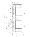
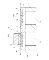
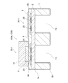
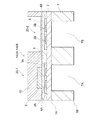
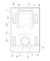
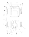
図1は、本実施形態の感熱素子を有する薄膜サーミスタ素子(20−1、20−2)の基本構成を示す平面図である。図2は、図1に示す薄膜サーミスタ素子(20−1、20−2)をA−A´線に沿って切断した断面図である。 FIG. 1 is a plan view showing a basic configuration of a thin film thermistor element (20-1, 20-2) having a thermal element of the present embodiment. FIG. 2 is a cross-sectional view of the thin film thermistor element (20-1, 20-2) shown in FIG. 1 cut along the line AA ′.
薄膜サーミスタ素子(20−1、20−2)は、基板1、絶縁膜2、2つの一対の取り出し電極(3A、3B)、サーミスタ薄膜(4A、4B)、保護膜6、取り出し電極(3A、3B)露出部上に形成された電極PAD(5A、5B)から構成され、所定の間隔をおいて形成される一対の取り出し電極(3A、3B)と、これらの取り出し電極(3A、3B)上および取り出し電極(3A、3B)間に成膜されるサーミスタ薄膜(4A、4B)とで構成されている。なお、感熱素子は、2つの一対の取り出し電極(3A、3B)、サーミスタ薄膜(4A、4B)を指す。
The thin film thermistor elements (20-1, 20-2) include a substrate 1, an insulating
基板1は、第1の主面1A、及び、その裏面である第2の主面1Bを有しており、少なくとも第1の主面1Aには絶縁膜2が形成されている。基板1の材質としては、適度な機械的強度を有し、且つエッチング等の微細加工に適した材質であればよく、特に限定されるものではないが、例えば、シリコン(Si)単結晶基板、サファイア単結晶基板、セラミックス基板、石英基板、ガラス基板等が好適である。絶縁膜2としては、適度な機械的強度を有し、且つ、公知の薄膜プロセスで容易に成膜できるものであればよく、特に限定されるものではないが、例えば、Si酸化膜、Si窒化膜等が好適である。
The substrate 1 has a first
また、基板1には、薄膜サーミスタ素子(20−1、20−2)が配置される位置に、より具体的には、サーミスタ薄膜(4A、4B)が配置される位置に対応してキャビティ(7A、7B)が形成される。キャビティ(7A、7B)は、第2の主面1B側から第1の主面1A側に向けて基板内部に凹部を有している。凹部は絶縁膜2が完全に露出していることが好ましいが熱容量が大きく増加することがなければ除去残りがあってもよい。なお、熱容量とは、所定の周波数を有する赤外線などのエネルギー源を材料が吸収することにより発生する熱エネルギーの比率を指す。つまり、材料の重量が増加すれば(例えば、膜厚が厚くなる)熱容量が増加し、同一のエネルギーに対して発熱速度は低下する。
Further, in the substrate 1, cavities (corresponding to positions where the thermistor thin films (4A, 4B) are arranged are arranged at positions where the thin film thermistor elements (20-1, 20-2) are arranged. 7A, 7B) are formed. The cavity (7A, 7B) has a concave portion inside the substrate from the second
絶縁膜2の上に一対の取り出し電極(3A、3B)が形成され、一対の取り出し電極(3A、3B)上および取り出し電極(3A、3B)間にサーミスタ薄膜(4A、4B)が形成される。また、サーミスタ薄膜(4A、4B)を被覆して外気から遮蔽するための保護膜6が形成されている。なお、保護膜6はサーミスタ薄膜(4A、4B)を外気から遮断する必要が無い構成であったり、吸収膜吸収層9、赤外線反射膜8および吸収膜保護層10が絶縁物で、サーミスタ薄膜(4A、4B)と導電が無い状態であれば必須ではない。取り出し電極(3A、3B)の材質としては、サーミスタ薄膜(4A、4B)の成膜工程や熱処理工程等に耐え得る耐熱性を有し、且つ、適度な伝導性を有する比較的高融点の材質が好ましく、例えば、モリブデン(Mo)、白金(Pt)、金(Au)、タングステン(W)、タンタル(Ta)、パラジウム(Pd)、イリジウム(Ir)、又はこれらの金属を2種類以上含む合金等が好適である。また電気信号を取り出すためには取り出し電極(3A、3B)に接続された電極PAD(5A、5B)が各々の取り出し電極(3A、3B)に接続されるように形成される。電極PAD(5A、5B)の材質としては、ワイヤーボンドやフリップチップボンディング等の電気的接続が容易な材質、例えば、アルミニウム(Al)、Au等が好適である。
A pair of extraction electrodes (3A, 3B) is formed on the insulating
薄膜サーミスタ素子(20−1)上には、保護膜6上に赤外線を吸収する吸収膜吸収層9が形成されている。吸収膜吸収層9はスピンコーターで基板1の第1の主面1A上に全面に塗布され、ベーク処理を用いて仮硬化した後、フォトリソグラフィの工程により露光、現像され、所望の形状にパターニングされる。あらかじめポア剤等を添加することによりアニーリング時やベーク時に吸収膜吸収層を多孔質化させても良い。なお、吸収膜吸収層9は、母材が第1の有機材料からなり、所望の形状にパターニング可能であれば副成分として赤外線を吸収する材料が含まれていても良い。ここで、副成分は、50wt%未満であれば良い。また、第1の有機材料は一種類とは限らず、所望の形状にパターニングされる有機材料全体を指す。
On the thin film thermistor element (20-1), an absorption
吸収膜吸収層9上には吸収膜保護層10が形成される。吸収膜保護層10はスピンコーターで基板1の第1の主面1A上に全面に塗布され、ベーク処理を用いて仮硬化した後、フォトリソグラフィの工程により露光、現像され、所望の形状にパターニングされる。ここで、吸収膜吸収層9の上面および側面である段差部は吸収膜保護層10によって、被覆されている。つまり、吸収膜吸収層9の形状を被覆する形で、吸収膜吸収層9の形状よりも大きく所望の形状にパターニングされる。また、吸収膜保護層10は吸収膜吸収層9よりも赤外線吸収効果の小さい有機材料が選択されている。このような材料選択と厚み、面積の大きさの選択は本来の吸収膜吸収層9の赤外線吸収特性を損なわないことを目的とする。吸収膜保護層10が吸収膜吸収層9より効果的な赤外線吸収効果をもつ材料であれば、吸収膜保護層10と吸収膜吸収層9とを合算した熱容量が増加するので、同一エネルギーに対する発熱速度は低下してしまうので、センサとしての応答速度は低下する。さらに、吸収膜保護層10が吸収した赤外線吸収による発生した熱量は、吸収膜保護層10とサーミスタ薄膜4A間の距離が吸収膜吸収層9とサーミスタ薄膜4A間の距離より長くなるため、サーミスタ薄膜4Aに伝達するまでの時間が長くなり、センサとしての応答速度はさらに低下する。又、吸収膜保護層10が吸収膜吸収層9を被覆することなく、吸収膜吸収層9より小さくパターニングされると、耐薬品に対する保護層としての役目を果たさない。
An absorption film
最後に基板1の第2の主面1Bをエッチングしてキャビティ(7A、7B)を形成する。ここで、キャビティ(7A、7B)に対応した領域をメンブレン領域とする。メンブレン領域は、キャビティ(7A、7B)上の基板1の第1の主面1Aの法線方向に存在する構造物を含む領域である。なお、本実施形態では感熱素子は検知素子感熱膜4Aおよび一対の取り出し電極3Aを指すものであるが、これに限るものではなく、検知素子感熱膜4Aはサーミスタ薄膜と異なる材料を使用してもよい。キャビティ7Aは吸収膜吸収層9と吸収膜保護層10の積層構造よりも基板の第1の主面1Aを法線とする平面で見た場合に、大きく形成される。また、吸収膜保護層10の端部がキャビティ7Aの上部、すなわちメンブレン領域の内部に存在することにより、赤外線吸収により発生した熱量をキャビティ7Aの外部に伝達しにくいようにすることが可能となる。よって、吸収膜吸収層9と吸収膜保護層10の積層構造内部に効果的に赤外線吸収により発生した熱量を閉じ込めることによって、赤外線に対して高感度なセンサを実現する効果が得られる。なお、サーミスタ薄膜(4A、4B)の端部は、対応するキャビティ(7A、7B)の上部、すなわちメンブレン領域の内部に存在してもよく、キャビティ(7A、7B)の外部に存在してもよい。また、取り出し電極(3A、3B)露出部のそれぞれの中心を結ぶ直線と概ね直交する方向の取り出し電極(3A、3B)のそれぞれの端部は対応するキャビティ(7A、7B)の上部、すなわちメンブレン領域の内部に存在してもよく、キャビティ(7A、7B)の外部に存在してもよい。
Finally, the second
(実施例)
本実施形態に基づく本実施例の、薄膜サーミスタ素子(20−1、20−2)の製造方法について説明する。薄膜サーミスタ素子(20−1、20−2)は赤外線センサ20として使用するため、2つのメンブレン領域のそれぞれに対応して検知側素子(20−1)と、参照側素子(20−2)とが隣接して形成される。検知側素子(20−1)とは赤外線を吸収し、発生した熱量を電気信号として検知する素子で本実施形態の吸収膜吸収層9と吸収膜保護層10の膜積層構造が形成される。又、参照側素子(20−2)は検知側素子(20−1)との比較の為、赤外線を反射する赤外線反射膜8が形成される。それぞれの素子の赤外線照射による変化量の差をブリッジ回路として出力とする赤外線センサ20となる。すなわち、参照側素子(20−2)は赤外線を反射するので実質的に環境温度を検知し、検知側素子(20−1)は環境温度と赤外線吸収とによる温度を検知するので、ブリッジ回路によって実質的に赤外線による変化量を求めることが可能となっている。
(Example)
The manufacturing method of the thin film thermistor element (20-1, 20-2) of this example based on this embodiment will be described. Since the thin film thermistor elements (20-1, 20-2) are used as the
図1と図2に示すように、基板1として、基板表面の面方位が(100)である(100)Si基板を用意し、基板1の第1の主面1Aに絶縁膜2としてSi酸化膜を成膜する。Si酸化膜を成膜するには、例えば、熱酸化法等を適用すればよい。絶縁膜2の膜厚は、基板1との絶縁性が確保される程度に調整すればよく、例えば、0.1μm〜1.0μm程度が好適である。本実施例では絶縁膜2として、二酸化珪素膜を0.5μm形成した。
As shown in FIG. 1 and FIG. 2, a (100) Si substrate having a substrate surface orientation of (100) is prepared as a substrate 1, and Si oxide is formed as an insulating
次に、第1の主面1A上の絶縁膜2上に一対の取り出し電極(3A、3B)を形成する。一対の取り出し電極(3A、3B)を形成するには、例えば、スパッタ法等を用いて絶縁膜2上に150nm〜600nm程度の一対の取り出し電極(3A、3B)となる金属薄膜(3A、3B)を堆積し、フォトリソグラフィ工程によってエッチングマスクを形成し、反応性イオンエッチングやイオンミリング等のドライエッチングでこの金属薄膜(3A、3B)を所定の電極形状に加工して、取り出し電極(3A、3B)を形成する。なお、金属薄膜である一対の取り出し電極(3A、3B)と絶縁膜2との間の密着性を高めるには、チタン(Ti)等の密着層を5〜10nm程度介在させるのが好ましい。本実施例では取り出し電極(3A、3B)としてPt/Ti膜を使用した。Ptはスパッタ法にて0.1μm形成し、密着層として、二酸化珪素と相性の良い、Tiを選択した。なお、Ptはスパッタ法にて100nm形成した。この後、ドライエッチングを用いて、一対の取り出し電極(3A、3B)を形成した。ここで、後述する取り出し電極(3A、3B)露出部のそれぞれの中心を結ぶ直線と概ね直交する方向の取り出し電極(3A、3B)のそれぞれの端部が、対応するキャビティ(7A、7B)の上部に存在するように形成した。
Next, a pair of extraction electrodes (3A, 3B) is formed on the insulating
次に、サーミスタ薄膜(4A、4B)としての複合金属酸化膜(4A、4B)を、スパッタ法により取り出し電極(3A、3B)上に堆積し、ウェットエッチングにより複合金属酸化膜(4A、4B)を所定形状にパターニングする。ここで、サーミスタ薄膜(4A、4B)は一対の取り出し電極(3A、3B)上の一部および一対の取り出し電極(3A、3B)間の一部に連続した形状でパターニングする。また、サーミスタ薄膜(4A、4B)の端部が対応するキャビティ(7A、7B)の外部に存在するようにパターニングした。すなわち、一対の取り出し電極(3A、3B)間に電圧を印加することにより発生する電流はサーミスタ薄膜(4A、4B)に流れる。本実施例では、基板温度600℃、成膜圧力1.0Pa、RFパワー200Wのスパッタ条件でArガスを用い、Mn−Co−Ni系酸化物を取り出し電極(3A、3B)上に0.4μm堆積した。次に、塩化第二鉄水溶液を用いたウェットエッチングで所定形状に加工し、焼成炉を用いてMn−Co−Ni系酸化物膜に大気雰囲気で600℃で2時間の熱処理を施した。 Next, a composite metal oxide film (4A, 4B) as a thermistor thin film (4A, 4B) is deposited on the extraction electrode (3A, 3B) by sputtering, and the composite metal oxide film (4A, 4B) by wet etching. Is patterned into a predetermined shape. Here, the thermistor thin film (4A, 4B) is patterned in a shape that is continuous with a part on the pair of extraction electrodes (3A, 3B) and a part between the pair of extraction electrodes (3A, 3B). Further, the thermistor thin films (4A, 4B) were patterned so that the end portions existed outside the corresponding cavities (7A, 7B). That is, current generated by applying a voltage between the pair of extraction electrodes (3A, 3B) flows through the thermistor thin film (4A, 4B). In this example, Ar gas is used under sputtering conditions of a substrate temperature of 600 ° C., a film forming pressure of 1.0 Pa, and an RF power of 200 W, and Mn—Co—Ni-based oxide is extracted to 0.4 μm on the electrodes (3A, 3B). Deposited. Next, it was processed into a predetermined shape by wet etching using an aqueous ferric chloride solution, and the Mn—Co—Ni-based oxide film was heat-treated at 600 ° C. for 2 hours in an air atmosphere using a baking furnace.
保護膜6として二酸化珪素膜を形成する。保護膜6としては二酸化珪素や窒化珪素等、絶縁性、耐湿性を有する膜であれば良い。本実施例では、テトラエトキシシランという有機金属材料を用いたTEOS−CVD法により、0.4μmの膜厚で二酸化珪素を基板全面に成膜した。
A silicon dioxide film is formed as the
次に検知側素子(20−1)上に吸収膜吸収層9をスピンコートにより塗布した。本実施例では3000rpm、30秒にて膜厚1.4μmで形成した。材料はネガ型感光性樹脂にカーボンが含まれる市販レジスト、ブラックマトリクスレジストを用いた。カーボンの含有量は10wt%であった。ベーク処理を用いて仮硬化した後、フォトリソグラフィの工程により露光、現像し、基板1の主面1Aの法線と直交する方向で、一対の取り出し電極(3A、3B)の電極間を完全に覆うようにパターニングした。
Next, the absorption
次に検知側素子(20−1)上に吸収膜保護層10をスピンコートにより塗布した。本実施例では3000rpm、30秒にて膜厚3.0μmで形成した。材料は市販されているポリイミド感光性樹脂を使用した。ベーク処理を用いて仮硬化した後、フォトリソグラフィの工程により露光、現像し、吸収膜吸収層9を完全に覆い、かつその端部がメンブレン領域の内部に存在するようにパターニングした。パターニング後に220℃120分のベークを行い完全硬化させた。
Next, the absorbing film
このとき、図15に示されるように赤外線センサ150は、吸収膜吸収層9および吸収膜保護層10が概ね円状または楕円状であり、かつ、基板1の第1の主面1Aの法線から見た場合に一対の取り出し電極3A間の一部と重なる形状で形成された場合である実施例2、及び、図16に示されるように赤外線センサ160は、吸収膜吸収層9および吸収膜保護層10が十字状であり、かつ、基板1の主面1Aの法線から見た場合に一対の取り出し電極3A間の一部と重なる形状で形成された場合である実施例3のように、吸収膜保護層10の形状が吸収膜吸収層9の形状をトレースする形で全面を覆うように形成することにより、収膜吸収層9が吸収した赤外線により発生する熱量のサーミスタ薄膜4A以外への放熱を低減することが可能となり、最適の感度となる。ここで、トレースする大きさは製造上のマージンを考慮して吸収膜保護層10の端部を可能な限り吸収膜吸収層9と近づけることが好ましい。通常、マージンは1μm以上10μm以下である。
At this time, as shown in FIG. 15, in the
さらに、選択する材料としては、吸収膜保護層10は吸収膜吸収層9よりも大きい赤外線透過特性を有することが好ましい。また、吸収膜保護層10と吸収膜吸収層9は、それらの積層構造における赤外線反射特性が吸収膜保護層10と吸収膜吸収層9の各々の赤外線反射特性に対し、同等かそれ以下の赤外線反射特性を持つことが好ましい。このように選択することにより最適な応答速度が得られる。以下に説明する。
Furthermore, as a material to be selected, it is preferable that the absorption film
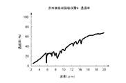
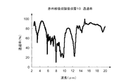
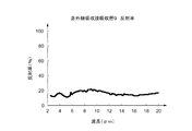
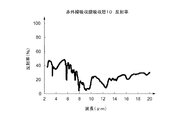
図7に吸収膜吸収層9、図8に吸収膜保護層10のFT―IR、いわゆるフーリエ変換型赤外分光法で評価した赤外線透過率の結果である。グラフの横軸は赤外線の波長(μm)、縦軸は透過率(%)を示す。つまり、図7、図8においては、透過率が低い程、赤外線の吸収効果が高いといえる。本実施例は、吸収膜吸収層9と吸収膜保護層10の主成分が有機材料であるため、ある特定の波長領域において特異的な透過率の減少が見られるが、図からみて明らかなように吸収膜保護層10のFT―IRの透過率は吸収膜吸収層9のFT―IRの透過率より大きいことがわかる。つまり、吸収膜保護層10側から入射する赤外線に対して、吸収膜保護層10は吸収膜吸収層9に対して赤外線の透過を阻害しない材料が選定されていることがわかる。これをデータで示すと、図9になる。図9は吸収膜吸収層9と吸収膜保護層10の第2の積層構造のFT―IRの透過特性であるが、図7と図9を比較しても大きく透過特性が変化していないことがわかる。従って、吸収膜吸収層9が赤外線を効率良く吸収することになりさらに、吸収膜保護層10が存在することにより、吸収膜保護層10が吸収膜吸収層9であると仮定した場合と比較して赤外線に対する熱容量の増加が低減されているので、赤外線吸収により発生する熱量をサーミスタ薄膜4に伝達することが可能となり、応答速度が速くなる。
FIG. 7 shows the results of infrared transmittance evaluated by FT-IR, that is, so-called Fourier transform infrared spectroscopy, of the absorbing
又、吸収膜保護層10の第2の有機材料は赤外線センサ20が使用される環境に応じて有機材料の種類を選択できるが、有機材料の種類によって材料の熱伝導率が異なり、熱伝導率の高い材料を使用した場合は赤外線からの熱を逃がしやすくする為、熱伝導率が低い材料を使用した場合より赤外線センサ20の出力が低下することが考えられる。しかし、吸収膜保護層10の端部をメンブレン領域の内部に形成することにより材料の熱伝導率による赤外線センサ20出力の低下を最小限に抑えることができる。本実施例1では熱伝導率が0.2(W/℃)のポリイミドを使用したが、実施例4として熱伝導率が5.0(W/℃)のシリコーン樹脂系材料を用い、形状、薄膜製作プロセスの条件は実施例1と同じにした赤外線センサ200を製作した。なお、シリコーン樹脂系材料は、膜厚3.0μmで形成した。また、FT―IRの赤外線透過率が実施例1のポリイミド感光性樹脂とほぼ同等となる材料を選択した。
The second organic material of the absorption film
図10、図11、図12はそれぞれ吸収膜吸収層9、吸収膜保護層10、吸収膜吸収層9と吸収膜保護層10の積層構造のFT―IRの反射特性である。図10、図11の各々のFT―IRの反射率と図12の積層構造の反射率を比較して積層構造の反射率が各々の反射率より小さくなるように積層構造が形成されていることがわかる。ここで、積層構造の反射率が小さくなっているので、吸収膜吸収層9が吸収した赤外線を吸収膜保護層10から外部に放出する割合を低減することが可能となっている。従って、高感度となる。さらに、吸収膜保護層10は吸収膜吸収層9よりも大きい赤外線透過特性を有する構成とすれば、より赤外線を効率よく吸収し、サーミスタ薄膜4に近い吸収膜吸収層9から赤外線吸収により発生する熱量をサーミスタ薄膜4に伝達することが可能となるので、より応答速度が速くなる。
10, 11, and 12 show the FT-IR reflection characteristics of the absorption
次に参照素子(20−2)上に赤外線反射膜8を形成した。反射膜材料は白金を使用し、リフトオフ法により所望の形状に形成した。赤外線反射膜8は赤外線センサ20内に入射した赤外線を感熱膜(4−B)に伝熱させないことが目的となる。ここで、赤外線反射膜8を基板2に垂直1の第1の主面1Aに垂直方向に投影した面は感熱膜(4−B)を全面で覆うことが好ましい。赤外線反射膜8側から入射する入射赤外線に対して感熱膜が反応しないことで、周囲温度の測定が可能になる。また、検知素子(20−1)の感熱膜(4−A)は赤外線および周囲温度により抵抗値が変化するので、感熱膜(4−B)と抵抗値に差が発生しその差を検出することで、赤外線を検知する赤外線センサ20となる。そのため、赤外線反射膜8に使用する材料は一般的に赤外線を効率よく反射する金属材料が使用され、中でも赤外線反射効率が良い白金が選択されることが多い。又、赤外線反射膜8として赤外線反射材料を用いても若干の温度上昇は発生するが赤外線反射膜8をメンブレン領域の外部まで形成することで、赤外線反射膜8の温度上昇を基板1に逃がすことができる点で好ましい。
Next, the infrared
次に、吸収膜保護層6の一部を反応性ドライエッチングにより除去し取り出し電極(3A、3B)露出部を形成し、取り出し電極(3A、3B)露出部上に電極PAD(5A、5B)をリフトオフ法により形成した。電極PAD(5A、5B)の材料はアルミニウム(Al)を使用した。ここで、電極PAD(5A、5B)はメンブレン領域の外部に形成した。
Next, a part of the absorption film
赤外線反射膜8及び電極PAD(5A、5B)の形成は吸収膜吸収層9と吸収膜保護層10を形成した後に行われる。理由は以下の通りである。第1に仮に、吸収膜吸収層9を形成する前に電極PAD(5A、5B)が絶縁膜2上に存在すると、金属PAD(5A、5B)と吸収膜吸収層9の母材である第1の有機材料が静電気力により密着し、吸収膜吸収層9の形成が困難になる。第2に、仮に、吸収膜保護層10を形成する前に赤外線反射膜8及び金属PAD(5A、5B)を形成すると、各プロセスにおけるフォトリソグラフィの剥離工程で使用する有機溶剤に吸収膜吸収層9の材料が耐えられない場合がある。
The infrared
最後に、基板1の第2の主面1B側に、フォトリソグラフィ工程によってエッチングマスクを形成した後、フッ化物系ガスを用いたD−RIE法等の反応性イオンエッチングによって、基板1を第2の主面1Bに対して垂直に深堀し、キャビティ(7A、7B)を開口する。D−RIE法とは、C4F8ガスを用いて反応抑止膜(フルオロカーボン系ポリマー)をキャビティ(7A、7B)の側壁に堆積させることにより、主としてFラジカルによる化学的なサイドエッチングを抑制するためのプラズマデポジション工程と、SF6ガスを用いてFラジカルによる基板1の化学的エッチングとFイオンによる反応抑止膜の物理的エッチングとにより、基板1を略垂直に異方性エッチングするためのプラズマエッチング工程とを交互に繰り返して基板1を深堀する方法である。
Finally, an etching mask is formed on the second
(評価)
以下に示す実施例及び比較例の赤外線センサについて、赤外線量を推定するための赤外線量に相当する出力電圧の測定を行った。出力電圧を得るための回路として、実施例の赤外線センサ20および比較例の赤外線センサについて図17に示す検知素子(20−1)と参照素子(20−2)とを含むフルブリッジ回路を用いた。以下に説明する。
(Evaluation)
For the infrared sensors of Examples and Comparative Examples shown below, the output voltage corresponding to the amount of infrared for estimating the amount of infrared was measured. As a circuit for obtaining an output voltage, a full bridge circuit including the detection element (20-1) and the reference element (20-2) shown in FIG. 17 was used for the
図17に示すフルブリッジ回路は、第1の基準抵抗R1の一端と抵抗THsを有する検知素子(20−1)の一端が接続され、第2の基準抵抗R1の他端が基準電位電源に接続され、抵抗THsを有する検知素子(20−1)の他端がGnd電位に接続され、第2の基準抵抗R2の一端と抵抗THrを有する参照素子(20−2)の一端が接続され、第2の基準抵抗R2の他端が基準電圧電源に接続され、抵抗THrを有する参照素子(20−2)の他端がGnd電位に接続され、第1の基準抵抗R1と抵抗THs有する検知素子(20−1)とのそれぞれの一端同士が接続された第1の接続P1から第1の出力電圧を出力し、第2の基準抵抗R2と抵抗THrを有する参照素子(20−2)とのそれぞれの一端同士が接続された第2の接続P2から第2の出力電圧を出力する。ここで、検知素子(20−1)と参照素子(20−2)とに対する外部からの赤外線吸収より発生する熱量以外の熱的影響を等しくする方が好ましい。このような抵抗差を利用した検知には、ハーフブリッジ回路もしくはフルブリッジ回路を用いる事が多いが、本実施例においては赤外線量に相当する出力電圧を得る部位に、フルブリッジ回路を用いる事が好ましい。 In the full bridge circuit shown in FIG. 17, one end of the first reference resistor R1 and one end of the sensing element (20-1) having the resistor THs are connected, and the other end of the second reference resistor R1 is connected to the reference potential power source. The other end of the sensing element (20-1) having the resistance THs is connected to the Gnd potential, one end of the second reference resistance R2 and one end of the reference element (20-2) having the resistance THr are connected, The other end of the second reference resistor R2 is connected to the reference voltage power source, the other end of the reference element (20-2) having the resistor THr is connected to the Gnd potential, and the sensing element having the first reference resistor R1 and the resistor THs ( The first output voltage is output from the first connection P1 in which one end of each of the reference elements 20-1) and 20-2) is connected to each of the reference element (20-2) having the second reference resistance R2 and the resistance THr. Second connection where one end of each is connected 2 and outputs a second output voltage. Here, it is preferable to equalize the thermal effects other than the amount of heat generated by infrared absorption from the outside with respect to the detection element (20-1) and the reference element (20-2). For detection using such a resistance difference, a half-bridge circuit or a full-bridge circuit is often used, but in this embodiment, a full-bridge circuit may be used for a portion that obtains an output voltage corresponding to the amount of infrared rays. preferable.
ここで、第1および第2の基準抵抗(R1、R2)の形状、組成を揃えることで、検知素子(20−1)の抵抗THsと参照素子(20−2)の抵抗THrとにおける外部からの赤外線吸収以により発生する熱量以外の熱的影響をほぼ等しくする事が出来る。 Here, by aligning the shape and composition of the first and second reference resistors (R1, R2), the resistance THs of the sensing element (20-1) and the resistance THr of the reference element (20-2) are externally applied. Thermal effects other than the amount of heat generated by the absorption of infrared rays can be made almost equal.
赤外線量に相当する出力電圧Pは、第1の接続点P1からの第1の出力電圧VP1と第2の接続点P2からの出力電圧VP2の電圧の差すなわち差電圧で得られる。検知素子(20−1)の抵抗THsと第1の基準抵抗R1との第1の接続点P1における第1の出力電圧VP1は赤外線量に応じて値が変化する。つまり検知素子(20−1)の抵抗THsが赤外線を受けたことによる温度上昇より伴い、抵抗が減少することにより第1の出力電圧VP1は小さくなる。一方参照素子(20−2)の抵抗THrと第2の抵抗R2との第2の接続点における第2の出力電圧VP2は赤外線からの影響はほとんど受けず、参照素子(20−2)の抵抗THrが赤外線以外の周囲温度の変化および放熱しきれない赤外線からのわずかな影響を伴った変化を示すことになる。従って、第1の出力電圧VP1と第2の出力電圧VP2の電圧の差すなわち差電圧、すなわち出力電圧Pは赤外線以外の周囲温度の影響を低減した赤外線量を示すことになり、出力電圧Pが大きいほど感度が良いことを示す。検知素子(20−1)と参照素子(20−2)は薄膜サーミスタであり、上述したように検知素子(20−1)と参照素子(20−2)とを隣接で配置した構造の赤外線温度センサ20である。
Output voltage P corresponding to the amount of infrared radiation is obtained at first the first and the output voltage V P1 second voltage difference or voltage difference between the output voltage V P2 from the connection point P2 from the connection point P1. The value of the first output voltage V P1 at the first connection point P1 between the resistance THs of the detection element (20-1) and the first reference resistance R1 changes according to the amount of infrared rays. That is, as the resistance THs of the detection element (20-1) receives the infrared rays, the first output voltage V P1 decreases as the resistance decreases as the temperature increases. While the second output voltage V P2 in resistance THr and the second connection point between the second resistor R2 of the reference element (20-2) is almost not undergo the influence of the infrared, the reference element (20-2) The resistance THr shows a change with a slight influence from an infrared ray that cannot be radiated and a change in ambient temperature other than the infrared ray. Therefore, the difference between the first output voltage V P1 and the second output voltage V P2 , that is, the difference voltage, that is, the output voltage P indicates the amount of infrared rays in which the influence of the ambient temperature other than infrared rays is reduced. It shows that a sensitivity is so good that P is large. The sensing element (20-1) and the reference element (20-2) are thin film thermistors, and as described above, the infrared temperature of the structure in which the sensing element (20-1) and the reference element (20-2) are arranged adjacent to each other. This is a
赤外線量の測定方法としては、所定温度に保持した赤外線温度センサ20に、実施例1から実施例3および以下に示す比較例について所定の赤外線を与えた時の、基準電圧Vcc(基準電圧電源の電圧)を印可した回路の第1の出力電圧VP1、第2の出力電圧VP2を測定する。
As a method for measuring the amount of infrared rays, the reference voltage Vcc (of the reference voltage power supply) when a predetermined infrared ray was applied to the
具体的には、検知素子(20−1)と参照素子(20−2)の2つの素子を隣接で配置した赤外線センサ20の温度を25℃に保ち、表面温度40℃に設定した測定対象としての平面黒体表面から5cm離して設置した時の、平面黒体の表面温度に対応する各測定点の電位すなわち第1の出力電圧VP1、第2の出力電圧VP2を測定した。
Specifically, as a measurement object in which the temperature of the
実施例1と実施例4の赤外線センサ(20、200)の出力特性を比較すると、吸収膜保護層10に0.2(W/℃)の熱伝導率をもつ第2の有機材料を使用した実施例1のセンサ出力と比較して吸収膜保護層10に5.0(W/℃)の熱伝導率をもつ第2の有機材料を使用した実施例4のセンサ出力は15%程低い結果となった。この出力差は吸収膜保護層10の熱伝導率の違いによるものであるが、熱伝導率が25倍異なる材料を使用しても、出力は15%程しか下がらない理由は、吸収膜保護層10の端部をメンブレン領域の内部に形成することで、赤外線から得た熱量を基板側にほとんど逃がすこと無く、感熱膜に伝えることができたためと考えられる。つまり、高感度となっている。
When the output characteristics of the infrared sensors (20, 200) of Example 1 and Example 4 are compared, the second organic material having a thermal conductivity of 0.2 (W / ° C.) is used for the absorbing film
(比較例1)
本実施例の効果を比較するために、図3に示すように、吸収膜吸収層9と吸収膜保護層10以外の構造を同じにして、吸収膜吸収層9と吸収膜保護層10を形成しない赤外線センサ30を製作して出力を実施例1と比較した。その結果を図6に示す。実施例1と比較して出力電圧Pが60%低下して40%となった。吸収膜吸収層9と吸収膜保護層10を形成しない状態と比較することにより、実際に吸収膜吸収層9と吸収膜保護層10の赤外線吸収効果がわかる。
(Comparative Example 1)
In order to compare the effects of the present embodiment, as shown in FIG. 3, the structure other than the absorption
(比較例2)
実施例の効果を比較するために、図4に示すように、吸収膜吸収層9と吸収膜保護層10以外の構造を同じにして、赤外線吸収膜として一般的に使用されている金黒膜を形成し、赤外線センサ40の出力を実施例1と比較した。金黒膜は低圧状態の蒸着法にて形成した。その結果を図6に示す。実施例1と比較して出力電圧Pが17%低下して83%となった。この結果より、一般的な吸収膜の金黒膜と比較しても同等以上の出力を得られていることがわかる。なお、金黒膜の膜厚は出力電圧Pが最大となる条件、すなわち、FT―IRで評価した赤外線透過率が最小となる3μmとした。
(Comparative Example 2)
In order to compare the effects of the examples, as shown in FIG. 4, a gold black film generally used as an infrared absorption film with the same structure except for the absorption
(比較例3)
本実施例の効果を比較するために、図5に示すように、吸収膜吸収層9を形成した後、吸収膜保護層10を赤外線吸収膜吸収層9と同じ材料で形成した。すなわち、吸収膜保護層10と吸収膜吸収層9の赤外線透過特性を同等にして赤外線吸収膜を形成した赤外線センサ50を製作して、図17に示すブリッジ回路にて出力特性及び、熱容量の増大による懸念項目のひとつである赤外線に対する応答速度を実施例1と比較した。結果を図6に示す。結果、出力電圧Pに関しては赤外線透過特性が同等になる為、ほぼ同等の結果であったが、全体の熱容量が増加したこと、および、入射した赤外線の吸収により吸収膜保護層10で発生した熱量が薄膜サーミスタに到達する時間が長くなるので赤外線に対する反応速度、すなわちセンサの応答速度が10%程悪化することがわかる。
(Comparative Example 3)
In order to compare the effects of this example, as shown in FIG. 5, after the absorption
(比較例4)
本実施例の効果を比較するために、図13に示すように、吸収膜保護層10をメンブレン領域の外部まで形成した。又、赤外線センサの多様性を考慮し、最外層膜となる吸収膜保護層10の熱伝導率による違いによる特性を比較する為、比較的に熱伝導率の小さい材料、今回は熱伝導率0.2(W/m℃)の有機材料、具体的にはポリイミドを使用し、他の構成は実施例1と同じにして赤外線センサ130Aを形成し、出力を実施例1と比較した。その結果を図18に示す。吸収膜保護層10をメンブレン領域の外部まで形成すると、吸収膜保護層10から基板1に赤外線吸収により発生する熱量の一部が逃げてしまう為、出力は本実施例1の95%ほどとなった。
(Comparative Example 4)
In order to compare the effects of the present example, as shown in FIG. 13, the absorbing film
(比較例5)
本実施例の効果を比較するために、図14に示すように、吸収膜保護層10を素子全面に形成した。尚、赤外線反射膜8を有する参照素子(20−2)上は入射する赤外線を反射する役目をもたせなければならない為、検知素子感熱膜4Bが存在するエリアのみフォトリソグラフィ工程により吸収膜保護層10を除去した。又、赤外線センサの多様性を考慮し、最外層膜となる吸収膜保護層10の熱伝導率による違いによる特性を比較する為、比較的に熱伝導率の小さい材料、今回は熱伝導率0.2(W/m℃)の有機材料、具体的にはポリイミドを使用し、他の構成は実施例1と同じにして赤外線センサ140Aを形成し、出力を実施例1と比較した。その結果を図18に示す。吸収膜保護層10をメンブレン領域の外部まで形成すると、吸収膜保護層10から基板1に赤外線吸収により発生する熱量の一部が逃げてしまう為、出力は本実施例1の93%ほどとなった。
(Comparative Example 5)
In order to compare the effects of this example, as shown in FIG. 14, an absorption film
(比較例6)
本実施例の効果を比較するために、図13に示すように、吸収膜保護層10をメンブレン領域の外部まで形成した。又、赤外線センサの多様性を考慮し、最外層膜となる吸収膜保護層10の熱伝導率による違いによる特性を比較する為、熱伝導率5.0(W/m℃)をもつシリコーン樹脂系材料を使用し、他の構成は同じにして赤外線センサ130Bを形成し、出力を実施例1と比較した。その結果を図18に示す。吸収膜保護層10をメンブレン領域の外部まで形成すると、吸収膜保護層10から基板1に赤外線吸収のより発生する熱量の一部が逃げてしまう現象は同じであるが、比較例4と比較して熱伝導率の影響を受けやすくなっていることがわかる。出力は本実施例1の41%ほどとなった。
(Comparative Example 6)
In order to compare the effects of the present example, as shown in FIG. 13, the absorbing film
(比較例7)
本実施例の効果を比較するために、図14に示すように、吸収膜保護層10を素子全面に形成した。尚、赤外線反射膜8を有する参照素子(20−2)上は入射する赤外線を反射する役目をもたせなければならない為、検知素子感熱膜4Bが存在するエリアのみフォトリソグラフィ工程により吸収膜保護層10を除去した。又、赤外線センサの多様性を考慮し、最外層膜となる吸収膜保護層10の熱伝導率による違いによる特性を比較する為、比較例4、比較例5で用いたポリイミドに対して吸水耐性があるが、熱伝導率が高い材料特性、熱伝導率5.0(W/m℃)をもつシリコーン樹脂系材料を使用し、他の構成は同じにして赤外線センサ140Bを形成し、出力を実施例1と比較した。その結果を図18に示す。吸収膜保護層10をメンブレン領域の外部まで形成すると、吸収膜保護層10から基板1に赤外線吸収により発生する熱量の一部が逃げてしまう現象は同じであるが、比較例5と比較して熱伝導率の影響を受けやすくなっていることがわかる。出力は本実施例1の39%ほどとなった。
(Comparative Example 7)
In order to compare the effects of this example, as shown in FIG. 14, an absorption film
(比較例8)
実施例の効果を比較するために、吸収膜吸収層9と吸収膜保護層10を、他の構造を同じにした状態で薄膜形成工程でのプロセス耐性を比較した。まず、薄膜形成工程における最終の工程、つまり、絶縁膜2を残存させ、かつ基板にキャビティ(7A、7B)を形成した後に吸収膜吸収層9の形成を試みたが、形成時にメンブレン領域の構造物が全て破壊されてしまった(比較例8−1)。次に保護層6を開口し、取り出し電極(3A、3B)露出部を形成し、露出部上に電極PAD(5A、5B)形成後、すなわち保護層6および絶縁膜2を残存させ、かつ基板にキャビティ(7A、7B)を形成する直前に吸収膜吸収層9を形成したが、電極PAD(5A、5B)は金属であり、ウェファー上には絶縁膜2の中に島状に点在する為、静電気を帯びてしまう。その静電気が絶縁材料である吸収膜吸収層9と強固に密着し、吸収膜吸収層9のパターニング形成後も電極PAD(5A、5B)形成後の吸収膜吸収層9が残ってしまった為、電気信号の導通がとれずこれも素子形成できなかった(比較例8−2)。これはその一つ前の工程である赤外線反射膜工程でも金属反射膜との密着により同じ結果となった(比較例8−3)。最後に保護膜6形成直後に吸収膜吸収層9のみを本実施例と同じ薄膜形成工程にて形成したが、この工程の後の赤外線反射膜形成工程にてフォトリソ工程のレジスト剥離に使用する有機溶剤にて吸収膜が無くなってしまった(比較例8−4)。一連の工程順序を図19に、素子形成不具合結果を図20に示す。
(Comparative Example 8)
In order to compare the effects of the examples, the process resistance in the thin film forming step was compared in the state where the absorption
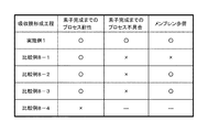
比較例8−4の問題は吸収膜吸収層9と吸収膜保護層10の積層構造により解決された。比較例8−1〜比較例8−3に示すように吸収膜吸収層9は最表面に金属が形成される前に形成することが最善である。吸収膜吸収層9形成の最適なプロセス位置は、取り出し電極(3A、3B)が保護膜6で完全に覆われている状態である。この状態であれば、ウェファー上は保護膜6で全面覆われており、金属材料の露出がない。すなわち、局部的な静電気は発生していない。しかし、この後のプロセスでは電極PAD(5A、5b)、赤外線反射膜8が取り出し電極(3A、3B)と同様に、絶縁膜上に島状に点在することになり、好ましくない。即ち、本実施例においては保護膜6形成直後に吸収膜吸収層9を形成することが最適となる。しかし、吸収膜吸収層9のみではその後の薄膜プロセス、例えば電極PAD(5A、5B)の形成や赤外線反射膜8の形成時に使用する有機溶剤、及び酸素プラズマ工程に耐えることができない。この問題は耐溶剤性、耐酸素プラズマ性のある有機材料を選択した吸収膜保護層10で吸収膜吸収層9を完全に覆うことで解決できる。そして吸収膜保護層10の端部をメンブレン領域の内部に形成することにより、実施例で示した通り、センサ出力の劣化も起きないのである。
The problem of Comparative Example 8-4 was solved by the laminated structure of the absorption
赤外線センサとして多種多様のアプリケーションに利用することができる。 It can be used for a wide variety of applications as an infrared sensor.
1 シリコン基板
2 絶縁膜
3A 検知素子取出電極
3B 参照素子取出電極
4A 検知素子感熱膜
4B 参照素子感熱膜
5A 検知素子電極PAD
5B 参照素子電極PAD
6 保護膜
7A 検知素子キャビティ
7B 参照素子キャビティ
8 赤外線反射膜
9 吸収膜吸収層
10 吸収膜保護層
20 赤外線センサ
20−1 検知素子
20−2 参照素子
DESCRIPTION OF SYMBOLS 1
5B Reference element electrode PAD
6
Claims (9)
前記基板内部に形成されたキャビティと、
前記キャビティに対応したメンブレン領域内に形成された感熱素子の上部に形成された母材が第1の有機材料である吸収膜吸収層と、
前記吸収膜吸収層上に形成されるとともに、前記吸収膜吸収層を被覆する第2の有機材料である吸収膜保護層とを有し、
前記吸収膜吸収層および前記吸収膜保護層の積層方向と直交する方向において、前記吸収膜保護層の端部が前記メンブレン領域の内部に形成された赤外線センサ。 A substrate,
A cavity formed in the substrate;
An absorption film absorption layer in which a base material formed on an upper part of a thermal element formed in a membrane region corresponding to the cavity is a first organic material;
An absorption film protective layer that is formed on the absorption film absorption layer and is a second organic material covering the absorption film absorption layer;
An infrared sensor in which an end portion of the absorption film protective layer is formed inside the membrane region in a direction orthogonal to a stacking direction of the absorption film absorption layer and the absorption film protection layer.
Priority Applications (1)
| Application Number | Priority Date | Filing Date | Title |
|---|---|---|---|
| JP2013067855A JP6142618B2 (en) | 2013-03-28 | 2013-03-28 | Infrared sensor |
Applications Claiming Priority (1)
| Application Number | Priority Date | Filing Date | Title |
|---|---|---|---|
| JP2013067855A JP6142618B2 (en) | 2013-03-28 | 2013-03-28 | Infrared sensor |
Publications (2)
| Publication Number | Publication Date |
|---|---|
| JP2014190894A true JP2014190894A (en) | 2014-10-06 |
| JP6142618B2 JP6142618B2 (en) | 2017-06-07 |
Family
ID=51837271
Family Applications (1)
| Application Number | Title | Priority Date | Filing Date |
|---|---|---|---|
| JP2013067855A Expired - Fee Related JP6142618B2 (en) | 2013-03-28 | 2013-03-28 | Infrared sensor |
Country Status (1)
| Country | Link |
|---|---|
| JP (1) | JP6142618B2 (en) |
Cited By (2)
| Publication number | Priority date | Publication date | Assignee | Title |
|---|---|---|---|---|
| WO2018110310A1 (en) * | 2016-12-14 | 2018-06-21 | 浜松ホトニクス株式会社 | Light detector |
| JP2018096877A (en) * | 2016-12-14 | 2018-06-21 | 浜松ホトニクス株式会社 | Photodetector |
Families Citing this family (1)
| Publication number | Priority date | Publication date | Assignee | Title |
|---|---|---|---|---|
| JP7164837B2 (en) * | 2020-02-21 | 2022-11-02 | Tdk株式会社 | pressure sensor |
Citations (8)
| Publication number | Priority date | Publication date | Assignee | Title |
|---|---|---|---|---|
| JPH05203487A (en) * | 1992-01-27 | 1993-08-10 | Matsushita Electric Works Ltd | Infrared light detector element |
| JPH06137938A (en) * | 1992-10-23 | 1994-05-20 | Matsushita Electric Works Ltd | Infrared detecting element |
| JPH09318454A (en) * | 1996-05-25 | 1997-12-12 | Horiba Ltd | Pyroelectric infrared ray thin film element |
| JP2006071601A (en) * | 2004-09-06 | 2006-03-16 | Denso Corp | Infrared sensor, infrared type gas detector, and infrared ray source |
| JP2008134113A (en) * | 2006-11-28 | 2008-06-12 | Hioki Ee Corp | Infrared sensor, and manufacturing method of infrared sensor |
| JP2008232896A (en) * | 2007-03-22 | 2008-10-02 | Toyohashi Univ Of Technology | Thin film infrared detecting element, and manufacturing method therefor |
| US20090250613A1 (en) * | 2008-04-07 | 2009-10-08 | University Of South Carolina | Chemically-Selective Detector and Methods Relating Thereto |
| JP2012008068A (en) * | 2010-06-28 | 2012-01-12 | Seiko Epson Corp | Pyroelectric detector, pyroelectric detection device, and electronic apparatus |
-
2013
- 2013-03-28 JP JP2013067855A patent/JP6142618B2/en not_active Expired - Fee Related
Patent Citations (8)
| Publication number | Priority date | Publication date | Assignee | Title |
|---|---|---|---|---|
| JPH05203487A (en) * | 1992-01-27 | 1993-08-10 | Matsushita Electric Works Ltd | Infrared light detector element |
| JPH06137938A (en) * | 1992-10-23 | 1994-05-20 | Matsushita Electric Works Ltd | Infrared detecting element |
| JPH09318454A (en) * | 1996-05-25 | 1997-12-12 | Horiba Ltd | Pyroelectric infrared ray thin film element |
| JP2006071601A (en) * | 2004-09-06 | 2006-03-16 | Denso Corp | Infrared sensor, infrared type gas detector, and infrared ray source |
| JP2008134113A (en) * | 2006-11-28 | 2008-06-12 | Hioki Ee Corp | Infrared sensor, and manufacturing method of infrared sensor |
| JP2008232896A (en) * | 2007-03-22 | 2008-10-02 | Toyohashi Univ Of Technology | Thin film infrared detecting element, and manufacturing method therefor |
| US20090250613A1 (en) * | 2008-04-07 | 2009-10-08 | University Of South Carolina | Chemically-Selective Detector and Methods Relating Thereto |
| JP2012008068A (en) * | 2010-06-28 | 2012-01-12 | Seiko Epson Corp | Pyroelectric detector, pyroelectric detection device, and electronic apparatus |
Cited By (6)
| Publication number | Priority date | Publication date | Assignee | Title |
|---|---|---|---|---|
| WO2018110310A1 (en) * | 2016-12-14 | 2018-06-21 | 浜松ホトニクス株式会社 | Light detector |
| JP2018096877A (en) * | 2016-12-14 | 2018-06-21 | 浜松ホトニクス株式会社 | Photodetector |
| WO2018110309A1 (en) * | 2016-12-14 | 2018-06-21 | 浜松ホトニクス株式会社 | Light detector |
| JP2018096878A (en) * | 2016-12-14 | 2018-06-21 | 浜松ホトニクス株式会社 | Photosensor |
| US10852194B2 (en) | 2016-12-14 | 2020-12-01 | Hamamatsu Photonics K.K. | Light detector |
| US11255730B2 (en) | 2016-12-14 | 2022-02-22 | Hamamatsu Photonics K.K. | Light detector |
Also Published As
| Publication number | Publication date |
|---|---|
| JP6142618B2 (en) | 2017-06-07 |
Similar Documents
| Publication | Publication Date | Title |
|---|---|---|
| US10782275B2 (en) | Semiconductor hydrogen sensor and manufacturing method thereof | |
| US7892488B2 (en) | Thermal liquid flow sensor and method of forming same | |
| US10197520B2 (en) | Integrated circuit with sensor and method of manufacturing such an integrated circuit | |
| CN101443635A (en) | Thermal mass gas flow sensor and method of forming same | |
| JP4590764B2 (en) | Gas sensor and manufacturing method thereof | |
| JP6142618B2 (en) | Infrared sensor | |
| US11435310B2 (en) | Humidity sensor | |
| CN106093138B (en) | Pass through the manufacturing method and sensor of the sensor of metal oxide detection gas | |
| JP5609919B2 (en) | Micro heater element | |
| KR100917792B1 (en) | Fabricating method for Micro Heater Having Reflection Thin Film and the same | |
| JP5672742B2 (en) | Infrared temperature sensor | |
| JP2009289838A (en) | Method of manufacturing sensor device | |
| JPH0590646A (en) | Thermopile type infrared sensor and its manufacture | |
| JP2007067398A (en) | Metal contact system for pressure sensor using semiconductor exposed to severe chemical and thermal environment as base | |
| WO2009145373A1 (en) | Packaging substrate and gas sensing device having the same, and method for manufacturing the same | |
| JP6003605B2 (en) | Infrared detector | |
| JP5821462B2 (en) | Infrared absorbing film and infrared detecting element using the same | |
| JP5803435B2 (en) | Infrared temperature sensor | |
| JP6340967B2 (en) | Gas sensor | |
| US8183111B1 (en) | Method of fabricating conductive electrodes on the front and backside of a thin film structure | |
| KR20190009918A (en) | A semiconductor gas sensor | |
| JP6155998B2 (en) | Infrared temperature sensor | |
| JPH06213707A (en) | Infrared sensor | |
| JP6245036B2 (en) | Infrared detector | |
| TWI836324B (en) | Microelectromechanical infrared sensing appartus and fabrication method thereof |
Legal Events
| Date | Code | Title | Description |
|---|---|---|---|
| A621 | Written request for application examination |
Free format text: JAPANESE INTERMEDIATE CODE: A621 Effective date: 20151214 |
|
| A977 | Report on retrieval |
Free format text: JAPANESE INTERMEDIATE CODE: A971007 Effective date: 20161125 |
|
| A131 | Notification of reasons for refusal |
Free format text: JAPANESE INTERMEDIATE CODE: A131 Effective date: 20161129 |
|
| A521 | Request for written amendment filed |
Free format text: JAPANESE INTERMEDIATE CODE: A523 Effective date: 20170116 |
|
| TRDD | Decision of grant or rejection written | ||
| A01 | Written decision to grant a patent or to grant a registration (utility model) |
Free format text: JAPANESE INTERMEDIATE CODE: A01 Effective date: 20170411 |
|
| A61 | First payment of annual fees (during grant procedure) |
Free format text: JAPANESE INTERMEDIATE CODE: A61 Effective date: 20170424 |
|
| R150 | Certificate of patent or registration of utility model |
Ref document number: 6142618 Country of ref document: JP Free format text: JAPANESE INTERMEDIATE CODE: R150 |
|
| LAPS | Cancellation because of no payment of annual fees |