JP2014178238A - Measurement device and measurement method - Google Patents
Measurement device and measurement method Download PDFInfo
- Publication number
- JP2014178238A JP2014178238A JP2013052982A JP2013052982A JP2014178238A JP 2014178238 A JP2014178238 A JP 2014178238A JP 2013052982 A JP2013052982 A JP 2013052982A JP 2013052982 A JP2013052982 A JP 2013052982A JP 2014178238 A JP2014178238 A JP 2014178238A
- Authority
- JP
- Japan
- Prior art keywords
- circuit
- measurement
- current
- switching
- output
- Prior art date
- Legal status (The legal status is an assumption and is not a legal conclusion. Google has not performed a legal analysis and makes no representation as to the accuracy of the status listed.)
- Granted
Links
- 238000005259 measurement Methods 0.000 title claims abstract description 158
- 238000000691 measurement method Methods 0.000 title claims abstract description 7
- 238000006243 chemical reaction Methods 0.000 claims abstract description 38
- 238000001514 detection method Methods 0.000 claims description 56
- 239000000284 extract Substances 0.000 claims description 2
- 230000009466 transformation Effects 0.000 claims description 2
- 238000012986 modification Methods 0.000 description 23
- 230000004048 modification Effects 0.000 description 23
- 238000012545 processing Methods 0.000 description 22
- 238000000034 method Methods 0.000 description 14
- 238000010586 diagram Methods 0.000 description 13
- 230000008569 process Effects 0.000 description 13
- 239000011162 core material Substances 0.000 description 7
- 230000005540 biological transmission Effects 0.000 description 6
- 230000008859 change Effects 0.000 description 6
- 230000000052 comparative effect Effects 0.000 description 6
- 238000012544 monitoring process Methods 0.000 description 5
- 230000007423 decrease Effects 0.000 description 2
- 238000003306 harvesting Methods 0.000 description 2
- 230000002093 peripheral effect Effects 0.000 description 2
- 238000004804 winding Methods 0.000 description 2
- 229910000976 Electrical steel Inorganic materials 0.000 description 1
- 239000003990 capacitor Substances 0.000 description 1
- 238000004891 communication Methods 0.000 description 1
- 238000013461 design Methods 0.000 description 1
- 230000000694 effects Effects 0.000 description 1
- 230000005669 field effect Effects 0.000 description 1
- 238000007689 inspection Methods 0.000 description 1
- 239000000463 material Substances 0.000 description 1
- 238000010248 power generation Methods 0.000 description 1
- 230000009467 reduction Effects 0.000 description 1
- 239000007787 solid Substances 0.000 description 1
- 238000012795 verification Methods 0.000 description 1
- 229910000859 α-Fe Inorganic materials 0.000 description 1
Images


Classifications
-
- G—PHYSICS
- G01—MEASURING; TESTING
- G01R—MEASURING ELECTRIC VARIABLES; MEASURING MAGNETIC VARIABLES
- G01R15/00—Details of measuring arrangements of the types provided for in groups G01R17/00 - G01R29/00, G01R33/00 - G01R33/26 or G01R35/00
- G01R15/14—Adaptations providing voltage or current isolation, e.g. for high-voltage or high-current networks
- G01R15/18—Adaptations providing voltage or current isolation, e.g. for high-voltage or high-current networks using inductive devices, e.g. transformers
-
- G—PHYSICS
- G01—MEASURING; TESTING
- G01R—MEASURING ELECTRIC VARIABLES; MEASURING MAGNETIC VARIABLES
- G01R19/00—Arrangements for measuring currents or voltages or for indicating presence or sign thereof
-
- G—PHYSICS
- G01—MEASURING; TESTING
- G01R—MEASURING ELECTRIC VARIABLES; MEASURING MAGNETIC VARIABLES
- G01R19/00—Arrangements for measuring currents or voltages or for indicating presence or sign thereof
- G01R19/0092—Arrangements for measuring currents or voltages or for indicating presence or sign thereof measuring current only
-
- G—PHYSICS
- G01—MEASURING; TESTING
- G01R—MEASURING ELECTRIC VARIABLES; MEASURING MAGNETIC VARIABLES
- G01R21/00—Arrangements for measuring electric power or power factor
Abstract
Description
本発明は、計測装置および計測方法であって、電流を計測する計測回路を備え、かつ、その電流を電源として利用する計測装置および計測方法に関する。 The present invention relates to a measurement device and a measurement method, which relate to a measurement device and a measurement method that include a measurement circuit that measures current and uses the current as a power source.
従来より、CT(Current Transformer)によって電流を取り出し、その電流を計測する計測装置が存在する。このような計測装置は、たとえば電気設備の消費電力を計測するために用いられる。 2. Description of the Related Art Conventionally, there is a measuring device that takes out current by CT (Current Transformer) and measures the current. Such a measuring device is used, for example, to measure the power consumption of an electrical facility.
特開2002−131344号公報(特許文献1)および特開2010−55356号公報(特許文献2)では、このような装置において、CTの出力電流を電源として利用することが開示されている。これにより、装置の配線が不要となるため、電気設備ごとに消費電力を細かく計測することができる。 Japanese Patent Application Laid-Open No. 2002-131344 (Patent Document 1) and Japanese Patent Application Laid-Open No. 2010-55356 (Patent Document 2) disclose that such an apparatus uses the output current of CT as a power source. Thereby, since wiring of an apparatus becomes unnecessary, power consumption can be measured finely for every electric equipment.
しかしながら、電流を計測する計測回路が電源回路と接続されている場合、電源回路と接続されていない場合よりも電流の計測精度が低下してしまう。 However, when the measurement circuit that measures current is connected to the power supply circuit, the current measurement accuracy is lower than when the measurement circuit is not connected to the power supply circuit.
本発明は、上記のような課題を解決するためになされたものであって、その目的は、精度良く電流を計測することのできる計測装置および計測方法を提供することである。 The present invention has been made to solve the above-described problems, and an object of the present invention is to provide a measuring apparatus and a measuring method capable of accurately measuring a current.
この発明のある局面に従う計測装置は、物理量を電流に変換するための物理量変換部と、物理量変換部の出力電流を計測する計測回路と、計測回路の出力を入力とする電源回路と、計測回路の出力を電源回路に入力する回路を構成する第1の状態と、計測回路の出力を物理量変換部に直接入力する回路を構成する第2の状態とを切替える回路切替手段と、電源回路によって駆動され、回路切替手段の制御を行う切替制御手段とを備える。切替制御手段は、待機時に回路切替手段を第1の状態となるように制御し、計測時には回路切替手段を第2の状態となるように制御することを特徴とする。 A measuring device according to an aspect of the present invention includes a physical quantity conversion unit for converting a physical quantity into a current, a measurement circuit that measures an output current of the physical quantity conversion unit, a power supply circuit that receives the output of the measurement circuit, and a measurement circuit Circuit switching means for switching between a first state that configures a circuit that inputs the output of the power supply circuit to the power supply circuit and a second state that configures a circuit that directly inputs the output of the measurement circuit to the physical quantity converter, and is driven by the power supply circuit Switching control means for controlling the circuit switching means. The switching control means controls the circuit switching means to be in a first state during standby, and controls the circuit switching means to be in a second state during measurement.
この発明の他の局面に従う計測装置は、物理量を電流に変換し、交流電流を取り出すための接続部を含む物理量変換部と、それぞれが接続部に流れる交流電流を直流電流に整流するための第1および第2の整流回路と、第1の整流回路における接地側の第1の整流素子のアノード側、および、第2の整流回路における接地側の第2の整流素子のアノード側の少なくとも一方に接続される検出部を含む、物理量変換部の出力電流を計測するための計測回路と、第1および第2の整流回路の出力を入力とする電源回路と、第1および第2の整流回路の出力を電源回路に入力する回路を構成する第1の状態と、計測回路の出力を物理量変換部に直接入力する回路を構成する第2の状態とを切替える回路切替手段と、電源回路によって駆動され、回路切替手段の制御を行う切替制御手段とを備える。切替制御手段は、待機時に回路切替手段を第1の状態となるように制御し、計測時には回路切替手段を第2の状態となるように制御することを特徴とする。 A measuring apparatus according to another aspect of the present invention includes a physical quantity conversion unit including a connection unit for converting a physical quantity into a current and taking out an alternating current, and a first unit for rectifying the alternating current flowing through the connection unit into a direct current. At least one of the first and second rectifier circuits, the anode side of the first rectifier element on the ground side in the first rectifier circuit, and the anode side of the second rectifier element on the ground side in the second rectifier circuit A measurement circuit for measuring the output current of the physical quantity conversion unit, including a connected detection unit, a power supply circuit that receives the outputs of the first and second rectifier circuits, and a first rectifier circuit and a second rectifier circuit. Driven by the power supply circuit, circuit switching means for switching between a first state constituting a circuit for inputting the output to the power supply circuit and a second state constituting a circuit for directly inputting the output of the measurement circuit to the physical quantity converter ,circuit And a switching control means for controlling the exchange unit. The switching control means controls the circuit switching means to be in a first state during standby, and controls the circuit switching means to be in a second state during measurement.
この発明のさらに他の局面に従う計測装置は、物理量を電流に変換し、交流電流を取り出すための接続部を含む物理量変換部と、物理量変換部による変換後の出力電流を直流電流に整流するための整流回路と、整流回路と並列接続され、物理量変換部の出力電流を計測する計測回路と、整流回路の出力を入力とする電源回路と、整流回路の出力を電源回路に入力する回路を構成する第1の状態と、計測回路の出力を物理量変換部に直接入力する回路を構成する第2の状態とを切替える回路切替手段と、電源回路によって駆動され、回路切替手段の制御を行う切替制御手段とを備える。切替制御手段は、待機時に回路切替手段を第1の状態となるように制御し、計測時には回路切替手段を第2の状態となるように制御することを特徴とする。 A measuring device according to still another aspect of the present invention converts a physical quantity into a current and rectifies an output current converted by the physical quantity conversion section into a direct current, including a physical quantity conversion section including a connection section for taking out an alternating current. Rectifier circuit, a measurement circuit that is connected in parallel with the rectifier circuit and measures the output current of the physical quantity converter, a power supply circuit that receives the output of the rectifier circuit, and a circuit that inputs the output of the rectifier circuit to the power supply circuit Circuit switching means for switching between a first state to be performed and a second state constituting a circuit for directly inputting the output of the measurement circuit to the physical quantity converter, and switching control driven by the power supply circuit to control the circuit switching means Means. The switching control means controls the circuit switching means to be in a first state during standby, and controls the circuit switching means to be in a second state during measurement.
この発明のさらに他の局面に従う計測方法は、電流を計測するための計測方法であって、物理量を電流に変換する変換ステップと、待機時に、計測回路の出力を電源回路に入力する回路を構成する第1の状態と計測回路の出力を物理量変換部に直接入力する回路を構成する第2の状態とを切替えるための回路切替部を、第1の状態となるように制御することで、変換ステップによる変換後の出力電流を電源回路に供給するステップと、待機時以外の期間に、回路切替部を第2の状態となるように制御することで、変換ステップによる変換後の出力電流を計測するステップとを含む。 A measurement method according to still another aspect of the present invention is a measurement method for measuring a current, and includes a conversion step for converting a physical quantity into a current and a circuit for inputting the output of the measurement circuit to a power supply circuit during standby. The circuit switching unit for switching between the first state to be switched and the second state constituting the circuit that directly inputs the output of the measurement circuit to the physical quantity conversion unit is controlled so as to be in the first state. Measuring the output current after conversion in the conversion step by supplying the output current after conversion in the step to the power supply circuit and controlling the circuit switching unit to be in the second state in a period other than the standby time Including the step of.
本発明によれば、精度良く電流を計測することができる。 According to the present invention, current can be measured with high accuracy.
本発明の実施の形態について図面を参照しながら詳細に説明する。なお、図中同一または相当部分には同一符号を付してその説明は繰返さない。 Embodiments of the present invention will be described in detail with reference to the drawings. In the drawings, the same or corresponding parts are denoted by the same reference numerals and description thereof will not be repeated.
<実施の形態1>
本実施の形態に係る計測装置は、物理量を電流に変換し、その電流を電源として利用する。電流への変換は、たとえば変流器としてのCTによって行われる。CTは、電力線に流れる電流を所定の変流比により変換して取り出す。この場合、物理量は電力である。
<
The measuring apparatus according to the present embodiment converts a physical quantity into a current and uses the current as a power source. Conversion to current is performed by CT as a current transformer, for example. The CT converts the current flowing through the power line with a predetermined current transformation ratio and takes it out. In this case, the physical quantity is electric power.
はじめに、本実施の形態に係る計測装置の概略構成について説明する。 First, a schematic configuration of the measurement apparatus according to the present embodiment will be described.
(概略構成について)
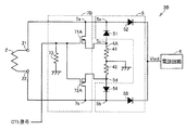
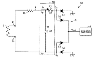
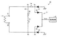
図1は、本発明の実施の形態1に係る計測装置1の構成図である。図1を参照して、計測装置1は、少なくとも、電力線9に流れる電流を計測する。本実施の形態に係る計測装置1は、電力線9に流れる電流を計測することで、電力線9を介して供給される電気設備における消費電力を計測する。計測装置1は、CT2と、CT2の二次側回路3として、計測回路4と、整流回路5と、電源回路6と、切替回路7とを備える。また、計測装置1は、CT2の二次側回路3に接続される監視部10をさらに備える。
(About schematic configuration)
FIG. 1 is a configuration diagram of a
CT2は、電力線1に流れる一次側電流Ifを二次側電流に変換し、1対の端子(接続部)21,22から取り出す。このようにして、CT2は、計測対象となる電流を抽出する。計測回路4は、CT2からの出力電流Isを計測する。計測回路4は、出力電流Isを検出するための検出部として、たとえば抵抗器40を含む。以下、この抵抗器を「検出抵抗器40」という。整流回路5は、交流電流である出力電流Isを直流電流に整流する。本実施の形態では、整流回路5は、検出抵抗器40の後段に設けられているが、検出抵抗器40の前段に設けてもよい。この場合、検出抵抗器40は、整流回路5により整流された電流を検出する。
The
電源回路6は、整流された直流電流を入力し、その電流を電源として使用する。電源回路6は、充電器61とDC/DCコンバータ62とを含む。充電器61は、たとえばキャパシタであるとするが、二次電池などであってもよい。DC/DCコンバータ62は、充電器61からの直流電圧を所定レベルに変換し、監視部10に電源を供給する。電源回路6の構成は、このような構成に限定されず、たとえば、充電器61の前段にコンバータなどが介在していてもよい。
The
切替回路7は、本実施の形態では、検出抵抗器40と整流回路5との接続部分に設けられる。切替回路7は、計測回路4と電源回路6とを電気的に接続および遮断する。つまり、切替回路7は、計測回路4の出力を電源回路5に入力する回路を構成する第1の状態と、計測回路4の出力をCT2に直接入力する回路を構成する第2の状態とを切替える。なお、本実施の形態において「直接入力する」とは、整流回路5および電源回路6を通ることなく入力することを意味している。したがって、第2の状態においては、計測回路4とCT2との間で電流の閉ループが形成される。切替回路7の詳細については後述する。
In the present embodiment, the switching circuit 7 is provided at a connection portion between the
監視部10は、電圧を検出するための電圧検出部11と、各種演算処理を実行する制御装置であるMPU(Micro-Processing Unit)12と、無線I/F(interface)13とを含む。監視部10の各部は、電源回路6によって駆動される。
The
電圧検出部11は、検出抵抗器40の両端の電位差を検出する。電圧検出部11には、電圧信号を増幅するためのオペアンプ(図示せず)、および、入力した電圧信号をデジタル信号に変換するためのA/D(Analog-to-Digital)コンバータ(図示せず)が含まれるものとする。電圧検出部11は、検出した電圧信号をMPU12に出力する。
The
MPU12は、CT2からの出力電流Isを計測する制御を行う。本実施の形態では、MPU12は、その機能構成として、電流を計測するための処理を実行する計測処理部121と、切替回路7の切替制御を行う切替制御部122とを含む。計測処理部121は、電圧検出部11から得られた電圧信号に基づいて、電気設備における消費電力を計算する。切替制御部122の具体的な制御についても後述する。
The
無線I/F13は、図示しない外部装置(コンピュータ)との間で無線通信を実行する。たとえば、無線I/F13は、計測処理部121による計測データを外部装置に送信する。
The wireless I /
本実施の形態に係る二次側回路3の詳細な説明に先立ち、一般的な二次側回路の構成について説明する。
Prior to detailed description of the
(一般的な二次側回路の構成について)
図17は、一般的な二次側回路103の構成を示す図である。図17を参照して、二次側回路103は、図1の二次側回路3と比較すると、切替回路7を含まない。二次側回路103において、CT2の一方の端子21は、検出抵抗器40(計測回路4)を介して整流回路5の一端5aに接続されている。CT2の他方の端子22は、整流回路5の他端5bに接続されている。整流回路5は、4つの整流素子51〜54で構成される。以下の説明において、一端5a側の2つの整流素子51,52で構成される回路を第1の整流回路、他端5b側の2つの整流素子53,54で構成される回路を第2の整流回路ともいう。
(General secondary circuit configuration)
FIG. 17 is a diagram showing a configuration of a general
このような二次側回路103の場合、電源回路6の入力側電圧(以下「電源電圧」という)Voutにより、CT2の一方の端子21に電圧負荷が加わる。そうすると、その電圧負荷によりCT2の変換特性(電流出力特性)に影響が出て、出力電流Isは理想値よりも減少する。つまり、電源電圧Voutが飽和電圧に達していなくても、端子21側に電圧負荷が加わることで、出力電流Isが低下してしまう。理想値とは、整流回路5と電源回路6が含まれていない、後述の図4に示すような二次側回路における出力電流の値に等しい。
In the case of such a
一方で、CT2が変換特性の優れたものである場合、電源電圧Voutの飽和電圧も大きくなるため、そのような影響が出にくい。したがって、図17のような二次側回路103によって電流を計測する場合、CT2としては、変換特性の優れたものを選定しておく必要がある。
On the other hand, when CT2 has an excellent conversion characteristic, the saturation voltage of the power supply voltage Vout also increases, so that such an effect is difficult to occur. Therefore, when the current is measured by the
図18は、一般的な二次側回路103を用いた場合の、CT2の出力電流の影響を示すグラフである。図18には、縦軸にCT2の出力電流Isの実効値(単位:uA)、横軸に電源電圧Vout(単位:V)をとったグラフが示されている。このグラフにおいて、ラインL100が理想出力を示し、ラインL101が変換特性の劣るCT(以下「第1のCT」という)の出力を示し、ラインL102が変換特性の良いCT(以下「第2のCT」という)を示している。第1のCTとしては、コア材質:ケイ素鋼、コア断面積:20mm2、コア周長さ:110mm、二次側巻数:3000巻のものが用いられている。第2のCTとしては、コア材質:フェライト、コア断面積:54.24mm2、コア周長さ:119.8mm、二次側巻数:3000巻のものが用いられている。つまり、第2のCTは、第1のCTよりも、コアの磁気抵抗が低く、かつ、大型である。また、これらは材質も異なる。そのため、第2のCTは、第1のCTよりも高価である。
FIG. 18 is a graph showing the influence of the output current of CT2 when the general
図18のラインL101に示されるように、第1のCTでは、電源電圧Voutが0Vであっても出力電流Isは理想値よりもかなり低い値となっている。ここで、第1のCTを用いた場合の、電源回路6に含まれる充電器61(図1)の充電特性を図19に示す。図19のグラフにおいて、ラインL201〜L204は、それぞれ、一次側電流Ifが2A、3A、4A、5Aである場合の充電器61の充電特性を示している。これらの図から分かるように、一般的な二次側回路103に第1のCTを用いた場合、計測精度を保証することはできない。
As indicated by the line L101 in FIG. 18, in the first CT, the output current Is is considerably lower than the ideal value even when the power supply voltage Vout is 0V. Here, FIG. 19 shows the charging characteristics of the charger 61 (FIG. 1) included in the
一方で、図18のラインL102に示されるように、第2のCTでは、電源電圧Voutが低い間は、出力電流Isは理想値に近い。しかしながら、第2のCTであっても、電源電圧Voutが高くなるにつれて、出力電流Isと理想値との差が広がっている。したがって、一般的な二次側回路103に第2のCTを用いた場合でも、精度良く電流(電力)を計測できないことが分かる。
On the other hand, as indicated by the line L102 in FIG. 18, in the second CT, the output current Is is close to the ideal value while the power supply voltage Vout is low. However, even in the second CT, the difference between the output current Is and the ideal value increases as the power supply voltage Vout increases. Therefore, it can be seen that even when the second CT is used for the general
そこで、本実施の形態では、間隔を置いて計測を行い、かつ、計測時には整流回路5および電源回路6を計測回路4から切り離すこととする。本実施の形態に係る二次側回路3の構成について、以下に詳細に説明する。
Therefore, in this embodiment, measurement is performed at intervals, and the
(本実施の形態に係る二次側回路について)
再び図1を参照して、本実施の形態に係る二次側回路3では、切替回路7が、検出部4の電流出力端側において、整流回路5に並列接続されている。したがって、CT2の一方の端子21は、検出抵抗器40を介して切替回路7の一端7aおよび整流回路5の一端5aに接続されている。CT2の他方の端子22は、切替回路7の他端7bおよび整流回路5の他端5bに接続されている。
(Secondary side circuit according to this embodiment)
Referring to FIG. 1 again, in
本実施の形態では、切替回路7は、1対のスイッチング素子として、同一極性のp型FET(Field effect transistor)71,72を含む。交流を±両方でoffするために、同一極性のFET71,72を逆向きに配置している。FET71のソースは、切替回路7の一端7aに接続されている。FET71のソースは、FET72のソースに接続されているとともに、所定電圧Vpull_upが供給されている。FET72のドレインは、切替回路7の他端7bに接続されている。FET72のゲートには、抵抗器73を介して所定電圧Vpull_upが与えられている。FET71,72のゲートには、MPU12の切替制御部122からの制御信号(CTL信号)が与えられる。なお、切替回路7は、3以上のスイッチング素子を含んでいてもよい。
In the present embodiment, switching circuit 7 includes p-type FETs (Field effect transistors) 71 and 72 having the same polarity as a pair of switching elements. The
FET71,72が非導通とされることで、計測回路4と電源回路6とが電気的に接続され、FET71,72が導通とされることで、計測回路4と電源回路6とが電気的に遮断される。FET71,72の制御は、MPU12の切替制御部122によって行われる。
When the
ここで、切替制御部122の制御に応じた出力電流Isの経路について説明する。本実施の形態において、計測時にFET71,72が導通され、少なくとも待機時にFET71,72が非導通とされる。なお、計測時とは、計測処理部121による計測処理が実行されている期間、すなわち電圧検出部11により検出抵抗器40の電圧が検出されている期間を表わす。また、待機時とは、少なくとも計測時を除外した期間である。本実施の形態では、計測データの処理時も待機時に含まれることとする。計測データの処理には、計測データの送信処理や、計測データの記録処理が含まれる。
Here, the path of the output current Is according to the control of the switching
図2は、本発明の実施の形態1に係る二次側回路3において、電力供給時の出力電流Isの経路を示す図である。図3は、本発明の実施の形態1に係る二次側回路3において、計測時の出力電流Isの経路を示す図である。
FIG. 2 is a diagram illustrating a path of the output current Is during power supply in the
図1および図2を参照して、切替制御部122は、待機時には、切替回路7のFET71,72をoff(非導通)としている。この場合、切替回路7の一端7aおよび他端7bは絶縁されるため、計測回路4(検出抵抗器40)を通った出力電流Isは、整流回路5へと流れる。したがって、充電器61は、整流回路5により整流された直流電流によって充電される。この場合の二次側回路3は、図17に示したような一般的な二次側回路103と同等の回路構成となる。
Referring to FIGS. 1 and 2, switching
一方、図1および図3を参照して、切替制御部122は、計測時には、切替回路7のFET71,72をon(導通)とする制御信号を出力する。この場合、切替回路7の一端7aおよび他端7bは電気的に接続される。ここで、FET71,72の接続部に印加する所定電圧Vpull_upは、接地電位(0V)と電源電圧Voutとの間で定められている。これにより、FET71,72が検出抵抗器40の電流出力端に接続される接点7aの電圧は、接地電位(0V)と電源電圧Voutとの間の値となるため、整流回路5の4つの整流素子(ダイオード)51〜54全てに、逆バイアス電圧がかかる。そのため、検出抵抗器40を通った出力電流Isは、整流回路5側へは流れずに、切替回路7の他端7bへと流れる。この場合の二次側回路3は、図4に示したような、電源回路6を有さない単純な計測回路104と同等の回路構成となる。電流計測が終わると、切替制御部122は、切替回路7のFET71,72を再びoffとする制御信号を出力する。
On the other hand, referring to FIGS. 1 and 3, switching
(動作について)
このような切替制御部122による切替制御を含む計測装置1の動作について説明する。
(About operation)
The operation of the measuring
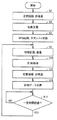
図5は、本発明の実施の形態1に係る計測装置1が実行する計測処理を示すフローチャートである。図5に示す計測処理は、MPU12が記憶部(図示せず)に格納されたプログラムを実行することで実現される。
FIG. 5 is a flowchart showing a measurement process executed by the
図1および図5を参照して、切替制御部122は、はじめ、切替回路7を非導通としている(ステップS2)。CT2が電力線9に取付けられ、出力電流Isが取り出されると、電源回路6の充電器61に対して初期充電が開始される(ステップS4)。その後、MPU12が起動されスタンバイ状態となる(ステップS6)。なお、ここでのスタンバイ状態は、MPU12におけるスタンバイ状態を意味しており、切替制御における待機状態(待機時)とは一致しない。
With reference to FIG. 1 and FIG. 5, the switching
MPU12がスタンバイ状態となると、計測処理のために、切替制御部122は、切替回路7を導通させる(ステップS8)。つまり、FET71,72のゲートにON信号を送信する。これにより、図3に示されるように、出力電流Isは、電源回路6(充電器61)側へ流れず計測回路4内を流れる。切替回路7が導通状態とされると、MPU12の計測処理部121は、計測処理を開始する(ステップS10)。計測処理部121による計測処理は、たとえば一定時間行われる。
When the
計測処理が終わると、切替制御部122は、切替回路7を再び非導通とする(ステップS12)。つまり、FET71,72のゲートにOFF信号を送信する。これにより、図2に示されるように、出力電流Isは、電源回路6側へ流れる。
When the measurement process ends, the switching
計測処理部121は、ステップS10での計測処理に基づく計測データを、外部装置に送信する(ステップS14)。具体的には、計測データが、無線I/F13を経由して外部装置に送信される。送信処理が終わると、MPU12は再びスタンバイ状態となる。
The
スタンバイ状態となってから、たとえば一定時間が経過すると(ステップS16にてYES)、ステップS8に戻り、上記処理が繰返される。なお、本実施の形態では、計測処理(ステップS10)の度に、計測データの送信(ステップS14)を行うこととしたが、たとえば所定回数ごとに計測データを送信してもよい。その場合、計測データは、自装置の記憶部(図示せず)、または、着脱可能な記録媒体(図示せず)に記録されており、計測データを送信する際に、記録された計測データが読み出されればよい。 If, for example, a certain period of time elapses after entering the standby state (YES in step S16), the process returns to step S8 and the above process is repeated. In the present embodiment, the measurement data is transmitted (step S14) every time the measurement process is performed (step S10). However, the measurement data may be transmitted every predetermined number of times, for example. In that case, the measurement data is recorded in a storage unit (not shown) of the device itself or a removable recording medium (not shown), and when the measurement data is transmitted, the recorded measurement data is It only has to be read out.
上述のように、本実施の形態によれば、計測時にのみ、切替回路7が導通とされ、その結果、二次側回路3は上述の「第2の状態」とされる。一方、待機時(本実施の形態では非計測時)には、切替回路7が非導通とされるため、二次側回路3は上述の「第1の状態」とされる。
As described above, according to the present embodiment, the switching circuit 7 is rendered conductive only during measurement, and as a result, the
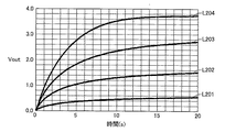
図6は、本発明の実施の形態1に係る計測装置1の第1の動作結果を示す図である。図7は、本発明の実施の形態1に係る計測装置1の第2の動作結果を示す図である。第1の動作結果には、CT2が、上記第1のCTで実装された場合における、各動作時の電源電圧Voutの変化が時間軸に沿って表わされている。第2の動作結果には、CT2が、上記第2のCTで実装された場合における、各動作時の電源電圧Voutの変化が時間軸に沿って表わされている。
FIG. 6 is a diagram showing a first operation result of the measuring
図6および図7における期間T1には、初期充電(図5のステップS4)の際の電圧変化が示されている。期間T2には、MPU12の起動(図5のステップS6)の際の電圧変化が示されている。期間T3には、計測処理および送信処理(図5のステップS10およびS14)が行なわれている際の電圧変化が示されている。期間T4には、MPU12がスタンバイ状態(図5のステップS16)の際の電圧変化が示されている。
In a period T1 in FIGS. 6 and 7, the voltage change during the initial charging (step S4 in FIG. 5) is shown. In the period T2, a voltage change at the time of starting the MPU 12 (step S6 in FIG. 5) is shown. In the period T3, a voltage change during the measurement process and the transmission process (steps S10 and S14 in FIG. 5) is shown. In the period T4, the voltage change when the
図6および図7に示されるように、計測処理および送信処理によって、電源電圧Voutは急降下する。しかしながら、一定期間(T4)充電を行うことで、CT2として第1のCTおよび第2のCTのどちらを用いたとしても、その後の計測処理および送信処理も適切に実行できる。このように、本実施の形態では、切替回路7を低消費電力のFET71,72で実現することで、上述のような切替制御を行っても電源回路6への電力供給に影響を与えることなく必要な処理(計測処理、送信処理など)を行うことができる。
As shown in FIGS. 6 and 7, the power supply voltage Vout rapidly drops due to the measurement process and the transmission process. However, by performing charging for a certain period (T4), the subsequent measurement process and transmission process can be appropriately executed regardless of which of the first CT and the second CT is used as CT2. As described above, in the present embodiment, the switching circuit 7 is realized by the
(検証結果)
最後に、上記動作による計測データの信頼性についての検証結果を示す。
(inspection result)
Finally, the verification result about the reliability of the measurement data by the said operation | movement is shown.
図8は、本発明の実施の形態1に係る計測装置1、および、比較例1,2における計測装置それぞれの計測誤差を示すグラフである。比較例1は、二次側回路が図17に示した回路103であり、かつ、CT2を第1のCTで実装した計測装置である。比較例2は、二次側回路が図17に示した回路103であり、かつ、CT2を第2のCTで実装した計測装置である。本実施の形態では、CT2が第1のCTで実装されている。
FIG. 8 is a graph showing measurement errors of the
図8には、横軸に電源電圧Vout(V)、縦軸に計測誤差(%)をとったグラフが示されている。計測誤差は、図4に示したような計測回路104での計測値(理想値)との誤差を示す。計測回路104は、計測回路4の後段に整流回路5および電源回路6を含まない構成である。図8において、比較例1での計測誤差がラインL11上に示され、比較例2での計測誤差がラインL12上に示されている。また、本実施形態での計測誤差がラインL10上に示されている。
FIG. 8 shows a graph in which the horizontal axis represents the power supply voltage Vout (V) and the vertical axis represents the measurement error (%). The measurement error indicates an error from a measurement value (ideal value) in the
切替回路7を含まない二次側回路103の場合、上述のように、出力電流Isに影響が出る。したがって、ラインL11に示されるように、変換特性の良くない第1のCTの場合、電源電圧Voutが0Vの時点であっても、誤差は70%を超えてしまう。また、ラインL12に示されるように、変換特性の良い第2のCTの場合でも、電源電圧Voutが上昇するにつれて誤差は上昇し、飽和電圧付近では、誤差は10%近くになる。
In the case of the
これに対し、ラインL10に示されるように、本実施の形態に係る計測装置1によれば、CT2を、変換特性の良くない第1のCTで実装した場合でも、電源電圧に関わらず測定誤差はほぼ0%であることが分かる。このように、本実施の形態によれば、CT2の変換特性にかかわらず、精度良く電流を計測することができる。その結果、装置の小型化およびコストダウンを図ることができる。
On the other hand, as shown by the line L10, according to the
<実施の形態2>
上記実施の形態1では、切替回路7を1対のp型FETにより実現したが、n型FETにより実現することもできる。以下に、実施の形態1との相違点のみ説明する。
<
In the first embodiment, the switching circuit 7 is realized by a pair of p-type FETs, but may be realized by an n-type FET. Only differences from the first embodiment will be described below.
図9は、本発明の実施の形態2に係る二次側回路3Aの構成を示す図である。図9において、図1に示した二次側回路3と同じ構成については、同じ符号を付してある。したがって、それらについての説明は繰り返さない。なお、以降の実施形態においても同様とする。
FIG. 9 is a diagram showing a configuration of the
図9を参照して、本実施の形態では、二次側回路3Aには、実施の形態1における切替回路7に代えて切替回路7Aが含まれる。切替回路7Aが接続される位置は、実施の形態1と同じである。
Referring to FIG. 9, in the present embodiment, switching
切替回路7Aは、同一極性の1対のn型FET71A,72Aを含む。FET71Aのドレインは、切替回路7の一端7aに接続されている。FET71のソースは、FET72のソースに接続されているとともに、所定電圧Vpull_downが供給されている。FET72Aのドレインは、切替回路7の他端7bに接続されている。FET72Aのゲートには、所定電圧Vpull_downが与えられている。FET71A,72Aのゲートには、MPU12の切替制御部122からの制御信号が与えられる。FET72Aのゲートには、抵抗器73を介して制御信号が与えられる。
The
本実施の形態においても、FET71A,72Aの接続部に印加する所定電圧Vpull_downは、接地電位(0V)と電源電圧Voutとの間で定められている。
Also in the present embodiment, the predetermined voltage Vpull_down applied to the connection part of the
なお、実施の形態1,2では、スイッチング素子として、p型またはn型のFETを採用したが、FETに限らずバイポーラトランジスタなどを採用してもよい。 In the first and second embodiments, the p-type or n-type FET is used as the switching element. However, the present invention is not limited to the FET, and a bipolar transistor or the like may be used.
<実施の形態3>
本実施の形態では、二次側回路において、検出抵抗器が接地電位と整流素子との間にある構成について説明する。ただし、この場合も、切替回路は、計測回路(検出抵抗器)と整流回路との接続部分に設けられる。以下に、実施の形態1との相違点のみ説明する。
<
In this embodiment, a configuration in which the detection resistor is between the ground potential and the rectifying element in the secondary side circuit will be described. However, also in this case, the switching circuit is provided at a connection portion between the measurement circuit (detection resistor) and the rectifier circuit. Only differences from the first embodiment will be described below.
図10は、本発明の実施の形態3に係る二次側回路3Bの構成を示す図である。図10を参照して、本実施の形態では、二次側回路3Bは、実施の形態1の計測回路4および切替回路7それぞれに代えて、計測回路4Aおよび切替回路7Bを含む。
FIG. 10 is a diagram illustrating a configuration of the secondary side circuit 3B according to the third embodiment of the present invention. Referring to FIG. 10, in the present embodiment, secondary circuit 3B includes
計測回路4Aは、整流素子51のアノード側5cに接続される検出抵抗器41と、整流素子54のアノード側5dに接続される検出抵抗器42とを含む。整流素子51は、第1の整流回路における接地側のダイオードである。整流素子54は、第2の整流回路における接地側のダイオードである。つまり、検出抵抗器41,42は、ともに一端が接地される。
The
本実施の形態では、電圧検出部11(図1)によって、検出抵抗器41,42それぞれの電圧が検出される。MPU12の計測処理部121(図1)は、それぞれの電圧に基づいて電力を計測する。なお、検出抵抗器41,42としては、計測時の電圧が電源電圧Voutを越えないものが選定されているものとする。
In the present embodiment, the voltages of the
切替回路7Bには、n型の2つのFET71A,72Aが含まれている。FET71Aは、CT2の端子21と、整流素子51のアノード側5cすなわち検出抵抗器41の他端との間に接続されている。FET72Aは、CT2の端子22と、整流素子54のアノード側5dすなわち検出抵抗器42の他端との間に接続されている。FET71A,72Aのゲートには、制御信号が与えられる。また、本実施の形態では、FET71A,72Aのゲートと接地間には、抵抗器73が接続されている。
The
本実施の形態においても、切替制御部122(図1)は、非計測時にFET71A,72Aを非導通とし、計測時にFET71A,72Aを導通状態とする。これにより、非計測時には、二次側回路3Bは、第1および第2の整流回路の出力を電源回路6に入力する回路を構成する状態とされる。また、計測時には、計測回路4Aの出力をCT2に直接入力する回路を構成する状態とされる。
Also in the present embodiment, the switching control unit 122 (FIG. 1) sets the
本実施の形態では、CT2の端子21と整流回路5の入力端子5aとの間に計測回路4Aが存在しない。そのため、非計測時にFET71A,72Aが非導通とされている場合、検出抵抗器41,42に高電圧が印加されないため、計測回路4Aを保護することができる。
In the present embodiment, there is no
(変形例)
実施の形態3では、計測回路4Aに、一端が接地された2つの検出抵抗器41,42を含めたが、いずれか一方のみを含んでいてもよい。この場合の二次側回路3Cを図11に示す。
(Modification)
In the third embodiment, the
図11を参照して、本変形例では、計測回路4Bに、たとえば、上記した検出抵抗器41のみが含まれている。この場合、電圧検出部11(図1)は、実施の形態1と同様に、検出抵抗器41の電圧のみを検出すればよい。
Referring to FIG. 11, in the present modification, for example, only the
なお、図10および図11では、切替回路7Bがn型のFET71A,72Aで実現された例が示されているが、p型FETなど他のスイッチング素子で実現してもよい。
10 and 11 show an example in which the
<実施の形態4>
上記実施の形態1〜3では、切替回路がスイッチング素子により実現されたが、スイッチング素子に限定されず、アナログスイッチや、ソリッドステートリレーによって実現されてもよい。本実施の形態では、切替回路をアナログスイッチで実現した場合の二次側回路の構成について説明する。
<
In the first to third embodiments, the switching circuit is realized by the switching element. However, the switching circuit is not limited to the switching element, and may be realized by an analog switch or a solid state relay. In this embodiment, the configuration of the secondary circuit when the switching circuit is realized by an analog switch will be described.
図12および図13は、本発明の実施の形態4に係る二次側回路3Dの構成を示す図である。図12および図13には、それぞれ、非計測時および計測時の出力電流Isの経路が示されている。
12 and 13 are diagrams showing the configuration of the
図12および図13を参照して、本実施の形態では、二次側回路3Dは、実施の形態1の切替回路7に代えて、切替回路7Cを含む。切替回路7Cは、2つのスイッチ74,75を含む。スイッチ75は、検出抵抗器40の電流出力端側において、整流回路5と並列接続されている。スイッチ74は、スイッチ75の検出抵抗器40側の端子7aよりも後段側において、検出抵抗器40と直列接続されている。より具体的には、スイッチ74,75は、一端が検出抵抗器40の電流出力端側(端子7a)に接続される。スイッチ74の他端は、整流回路5の一端5aに接続されている。スイッチ75の他端は、CT2の端子22と整流回路5の他端5bとの間(端子7b)に接続される。
12 and 13, in the present embodiment,
図12に示されるように、非計測時には、切替制御部122(図1)によって、スイッチ75がoffされ、スイッチ74がonされる。これにより、端子7aおよび端子7b間は絶縁され、端子7aおよび整流回路の一端5a間は電気的に接続される。したがって、出力電流Isは、整流回路5側にのみ流れ、電源回路6に電力が供給される。
As shown in FIG. 12, at the time of non-measurement, the
これに対し、図13に示されるように、計測時には、スイッチ75がonされ、スイッチ74がoffされる。これにより、端子7aおよび端子7b間は電気的に接続され、端子7aおよび整流回路の一端5a間は絶縁される。したがって、出力電流Isは、整流回路5へは流れず、計測回路4のみを流れる。
On the other hand, as shown in FIG. 13, at the time of measurement, the
なお、本実施の形態のように、切替回路を1対のアナログスイッチで実現する場合、スイッチを動作させるために電源が必要となる。したがって、本実施の形態に係る計測装置は、スイッチの動作用に、たとえば一次電池(図示せず)などを別途搭載していることが望ましい。 Note that when the switching circuit is realized by a pair of analog switches as in this embodiment, a power source is required to operate the switches. Therefore, it is desirable that the measuring apparatus according to the present embodiment is separately mounted with a primary battery (not shown), for example, for the operation of the switch.
(変形例1)
実施の形態4では、電力供給時(非計測時)にも、出力電流Isが検出抵抗器を通過する構成であったが、電力供給時には、検出抵抗器を通過しない構成としてもよい。
(Modification 1)
In the fourth embodiment, the output current Is passes through the detection resistor even when power is supplied (not measured). However, the configuration may be such that the detection current does not pass through when the power is supplied.
図14は、本発明の実施の形態4の変形例1に係る二次側回路3Eの構成を示す図である。図14を参照して、本変形例では、検出抵抗器40が整流回路5と並列接続されている。並列回路の一端および他端をそれぞれ端子8a,8bとして示している。この場合、スイッチ74は、端子8aと整流回路5の一端5aとの間に接続されている。スイッチ75は、並列回路において、検出抵抗器40の電流出力端側に直列接続されている。
FIG. 14 is a diagram showing a configuration of
切替制御部122(図1)による切替制御は、実施の形態4と同じである。その結果、二次側回路3Eは、非計測時に、整流回路5の出力を電源回路6に入力する回路を構成する状態とされる。また、計測時に、計測回路4Cの出力をCT2に直接入力する回路を構成する状態とされる。
The switching control by the switching control unit 122 (FIG. 1) is the same as that in the fourth embodiment. As a result, the
(変形例2)
また、上記変形例1のように、検出抵抗器40を整流回路5と並列接続する場合、図15のような構成としてもよい。
(Modification 2)
Further, when the
図15は、本発明の実施の形態4の変形例2に係る二次側回路3Fの構成を示す図である。図15を参照して、本変形例では、スイッチ74の位置が図14とは異なる。本変形例では、検出抵抗器40とスイッチ75との間の接続点8cに、所定電圧Vpull_upが供給されており、その電圧供給経路上に、スイッチ74が接続されている。
FIG. 15 is a diagram showing a configuration of
この場合、切替制御部122(図1)は、非計測時に、スイッチ74,75をoffし、計測時に、スイッチ74,75をonする。ここでも、電圧Vpull_upは、接地電位(0V)と電源回路6への出力電圧Voutとの間で定められている。これにより、整流回路5の4つの整流ダイオード51〜54全てに逆バイアス電圧がかかる。そのため、計測時には、出力電流Isは、端子8aを経由して検出抵抗器40側にのみ流れる。
In this case, the switching control unit 122 (FIG. 1) turns off the
(変形例3)
あるいは、検出抵抗器40を整流回路5と並列接続する場合、図16のような構成としてもよい。
(Modification 3)
Alternatively, when the
図16は、本発明の実施の形態4の変形例3に係る二次側回路3Gの構成を示す図である。図16を参照して、本変形例では、スイッチ74の位置が図15とは異なる。本変形例でも、検出抵抗器40とスイッチ75との間の接続点8cに、所定電圧Vpull_upが供給されている。スイッチ74は、並列回路において、検出抵抗器40の電流入力端側に直列接続されている。この場合のスイッチ74a,75の切替制御は、上記変形例2と同様である。
FIG. 16 is a diagram showing a configuration of a
以上説明したように、各実施形態および各変形例では、計測時に計測回路(検出抵抗器)から電源回路が電気的に切り離されるため、計測精度を向上させることができる。したがって、物理量を電流に変換する素子として小型かつ磁気抵抗の高いCTを1つ搭載するだけで、電流の計測と電力供給とを適切に行うことができる。その結果、計測装置の小型化およびコストダウンを図ることができる。 As described above, in each embodiment and each modification, since the power supply circuit is electrically disconnected from the measurement circuit (detection resistor) at the time of measurement, the measurement accuracy can be improved. Therefore, current measurement and power supply can be appropriately performed only by mounting one small CT having a high magnetic resistance as an element for converting a physical quantity into a current. As a result, it is possible to reduce the size and cost of the measuring device.
なお、各実施形態および各変形例では、CTによって電力が電流に変換される例を示したが限定的ではない。たとえば、エナジーハーベスト(環境発電)などによって、他の物理量が電流に変換されてもよい。計測対象の物理量としては、たとえば、i)風力量、ii)水力量、iii)熱量、iv)照度、などが挙げられる。これらの場合、図1に示した計測処理部121は、計測回路にて電流または電圧を検出し、各物理量を計測(演算)する。物理量が、i)風力量およびii)水力量の場合、変換素子としてはモータが採用される。物理量が、iii)熱量の場合、変換素子としてはペルチェ素子が採用される。物理量が、iv)照度の場合、変換素子としては光電素子が採用される。
In each embodiment and each modification, an example in which electric power is converted into current by CT has been described, but the present invention is not limited thereto. For example, other physical quantities may be converted into current by energy harvesting (energy harvesting) or the like. Examples of the physical quantity to be measured include i) wind quantity, ii) hydraulic quantity, iii) heat quantity, iv) illuminance, and the like. In these cases, the
変換素子が上記のような場合であっても、発電量に対し、相対的に後段の電源電圧が高くなる場合に計測精度に影響を及ぼすことがある。より具体的には、変換素子がモータの場合、電源電圧により、モータの回転に不要なトルクがかかり出力が低下してしまうことがある。また、変換素子がペルチェ素子および光電素子の場合、CTの場合と同様に、電源電圧により、素子間に発生した電圧に応じた電流が出力されなくなることがある。そのため、使用可能な素子が限られ、製品設計の自由度が大きく制限されることがあった。しかし、上記各実施の形態および各変形例のような二次側回路を用いることで、使用可能な素子が限定されることがなくなる。したがって、いずれの場合であっても、計測装置の小型化やコストダウンを図ることができる。 Even in the case where the conversion element is as described above, the measurement accuracy may be affected when the power supply voltage in the subsequent stage is relatively high with respect to the power generation amount. More specifically, when the conversion element is a motor, an unnecessary torque may be applied to the rotation of the motor due to the power supply voltage, and the output may decrease. Further, when the conversion element is a Peltier element or a photoelectric element, the current corresponding to the voltage generated between the elements may not be output due to the power supply voltage, as in the case of CT. Therefore, usable elements are limited, and the degree of freedom in product design may be greatly limited. However, by using the secondary side circuit as in each of the above embodiments and modifications, usable elements are not limited. Therefore, in any case, it is possible to reduce the size and cost of the measuring device.
今回開示された実施の形態はすべての点で例示であって制限的なものではないと考えられるべきである。本発明の範囲は上記した説明ではなくて特許請求の範囲によって示され、特許請求の範囲と均等の意味および範囲内でのすべての変更が含まれることが意図される。 The embodiment disclosed this time should be considered as illustrative in all points and not restrictive. The scope of the present invention is defined by the terms of the claims, rather than the description above, and is intended to include any modifications within the scope and meaning equivalent to the terms of the claims.
1 計測装置、2 CT(変流器)、3,3A,3B,3C,3D,3E,3F,3G 二次側回路、4,4A,4B,104 計測回路、5 整流回路、6 電源回路、7,7A,7B,7C 切替回路、9 電力線、10 監視部、11 電圧検出部、12 MPU、13 無線I/F、40,41,42 検出抵抗器、51,52,53,54 整流素子、61 充電器、62 DC/DCコンバータ、71,71A,72,72A FET、73 抵抗器、121 計測処理部、122 切替制御部。 1 measurement device, 2 CT (current transformer), 3, 3A, 3B, 3C, 3D, 3E, 3F, 3G secondary side circuit, 4, 4A, 4B, 104 measurement circuit, 5 rectifier circuit, 6 power supply circuit, 7, 7A, 7B, 7C switching circuit, 9 power line, 10 monitoring unit, 11 voltage detection unit, 12 MPU, 13 wireless I / F, 40, 41, 42 detection resistor, 51, 52, 53, 54 rectifying element, 61 charger, 62 DC / DC converter, 71, 71A, 72, 72A FET, 73 resistor, 121 measurement processing unit, 122 switching control unit.
Claims (11)
前記物理量変換部の出力電流を計測する計測回路と、
前記計測回路の出力を入力とする電源回路と、
前記計測回路の出力を前記電源回路に入力する回路を構成する第1の状態と、前記計測回路の出力を前記物理量変換部に直接入力する回路を構成する第2の状態とを切替える回路切替手段と、
前記電源回路によって駆動され、前記回路切替手段の制御を行う切替制御手段とを備え、
前記切替制御手段は、待機時に前記回路切替手段を前記第1の状態となるように制御し、計測時には前記回路切替手段を前記第2の状態となるように制御することを特徴とする、計測装置。 A physical quantity converter for converting a physical quantity into an electric current;
A measurement circuit for measuring an output current of the physical quantity converter;
A power supply circuit that receives the output of the measurement circuit;
Circuit switching means for switching between a first state constituting a circuit for inputting the output of the measurement circuit to the power supply circuit and a second state constituting a circuit for directly inputting the output of the measurement circuit to the physical quantity converter When,
A switching control unit that is driven by the power supply circuit and controls the circuit switching unit;
The switching control means controls the circuit switching means to be in the first state during standby, and controls the circuit switching means to be in the second state during measurement. apparatus.
前記物理量変換部による変換後の出力電流を直流電流に整流するための整流回路をさらに備える、請求項1に記載の計測装置。 The output current of the physical quantity converter is alternating current,
The measuring device according to claim 1, further comprising a rectifier circuit for rectifying the output current after conversion by the physical quantity converter into a direct current.
前記計測回路は、電流を検出するための検出部を含み、
前記検出部の電流入力端は、前記接続部の一方に接続され、
前記整流回路は、前記検出部の電流出力端側に接続され、
前記回路切替手段は、前記検出部の電流出力端側と前記整流回路との間に接続されている、請求項2に記載の計測装置。 The physical quantity conversion unit includes a connection unit for taking out an alternating current,
The measurement circuit includes a detection unit for detecting current,
The current input terminal of the detection unit is connected to one of the connection units,
The rectifier circuit is connected to a current output end side of the detection unit,
The measurement device according to claim 2, wherein the circuit switching unit is connected between a current output end side of the detection unit and the rectifier circuit.
それぞれが前記接続部に流れる交流電流を直流電流に整流するための第1および第2の整流回路と、
前記第1の整流回路における接地側の第1の整流素子のアノード側、および、前記第2の整流回路における接地側の第2の整流素子のアノード側の少なくとも一方に接続される検出部を含む、前記物理量変換部の出力電流を計測するための計測回路と、
前記第1および第2の整流回路の出力を入力とする電源回路と、
前記第1および第2の整流回路の出力を前記電源回路に入力する回路を構成する第1の状態と、前記計測回路の出力を前記物理量変換部に直接入力する回路を構成する第2の状態とを切替える回路切替手段と、
前記電源回路によって駆動され、前記回路切替手段の制御を行う切替制御手段とを備え、
前記切替制御手段は、待機時に前記回路切替手段を前記第1の状態となるように制御し、計測時には前記回路切替手段を前記第2の状態となるように制御することを特徴とする、計測装置。 A physical quantity converter including a connection for converting a physical quantity into an electric current and taking out an alternating current;
First and second rectifier circuits each for rectifying an alternating current flowing through the connecting portion into a direct current;
A detector connected to at least one of an anode side of the first rectifier element on the ground side in the first rectifier circuit and an anode side of the second rectifier element on the ground side in the second rectifier circuit; , A measurement circuit for measuring the output current of the physical quantity converter,
A power supply circuit having inputs of outputs of the first and second rectifier circuits;
A first state that configures a circuit that inputs the outputs of the first and second rectifier circuits to the power supply circuit, and a second state that configures a circuit that directly inputs the output of the measurement circuit to the physical quantity converter Circuit switching means for switching between,
A switching control unit that is driven by the power supply circuit and controls the circuit switching unit;
The switching control means controls the circuit switching means to be in the first state during standby, and controls the circuit switching means to be in the second state during measurement. apparatus.
前記物理量変換部による変換後の出力電流を直流電流に整流するための整流回路と、
前記整流回路と並列接続され、前記物理量変換部の出力電流を計測する計測回路と、
前記整流回路の出力を入力とする電源回路と、
前記整流回路の出力を前記電源回路に入力する回路を構成する第1の状態と、前記計測回路の出力を前記物理量変換部に直接入力する回路を構成する第2の状態とを切替える回路切替手段と、
前記電源回路によって駆動され、前記回路切替手段の制御を行う切替制御手段とを備え、
前記切替制御手段は、待機時に前記回路切替手段を前記第1の状態となるように制御し、計測時には前記回路切替手段を前記第2の状態となるように制御することを特徴とする、計測装置。 A physical quantity converter including a connection for converting a physical quantity into an electric current and taking out an alternating current;
A rectifier circuit for rectifying the output current after conversion by the physical quantity converter into a direct current;
A measurement circuit connected in parallel with the rectifier circuit and measuring an output current of the physical quantity converter;
A power supply circuit having the output of the rectifier circuit as an input;
Circuit switching means for switching between a first state constituting a circuit for inputting the output of the rectifier circuit to the power supply circuit and a second state constituting a circuit for directly inputting the output of the measurement circuit to the physical quantity converter When,
A switching control unit that is driven by the power supply circuit and controls the circuit switching unit;
The switching control means controls the circuit switching means to be in the first state during standby, and controls the circuit switching means to be in the second state during measurement. apparatus.
物理量を電流に変換する変換ステップと、
待機時に、計測回路の出力を電源回路に入力する回路を構成する第1の状態と前記計測回路の出力を前記物理量変換部に直接入力する回路を構成する第2の状態とを切替えるための回路切替部を、前記第1の状態となるように制御することで、前記変換ステップによる変換後の出力電流を前記電源回路に供給するステップと、
前記待機時以外の期間に、前記回路切替部を前記第2の状態となるように制御することで、前記変換ステップによる変換後の出力電流を計測するステップとを含む、計測方法。 A measurement method for measuring current,
A conversion step for converting a physical quantity into an electric current;
A circuit for switching between a first state constituting a circuit for inputting the output of the measurement circuit to the power supply circuit and a second state constituting a circuit for directly inputting the output of the measurement circuit to the physical quantity converter during standby Supplying the output current after conversion in the conversion step to the power supply circuit by controlling the switching unit to be in the first state;
Measuring the output current after the conversion in the conversion step by controlling the circuit switching unit to be in the second state during a period other than the standby time.
Priority Applications (6)
| Application Number | Priority Date | Filing Date | Title |
|---|---|---|---|
| JP2013052982A JP6171429B2 (en) | 2013-03-15 | 2013-03-15 | Measuring device and measuring method |
| EP14762751.7A EP2975416B1 (en) | 2013-03-15 | 2014-01-22 | Measuring apparatus and measuring method |
| US14/776,840 US9945887B2 (en) | 2013-03-15 | 2014-01-22 | Measuring apparatus and measuring method |
| CN201480012921.8A CN105026940B (en) | 2013-03-15 | 2014-01-22 | measuring device and measuring method |
| KR1020157024796A KR101750644B1 (en) | 2013-03-15 | 2014-01-22 | Measuring apparatus and measuring method |
| PCT/JP2014/051186 WO2014141746A1 (en) | 2013-03-15 | 2014-01-22 | Measuring apparatus and measuring method |
Applications Claiming Priority (1)
| Application Number | Priority Date | Filing Date | Title |
|---|---|---|---|
| JP2013052982A JP6171429B2 (en) | 2013-03-15 | 2013-03-15 | Measuring device and measuring method |
Publications (2)
| Publication Number | Publication Date |
|---|---|
| JP2014178238A true JP2014178238A (en) | 2014-09-25 |
| JP6171429B2 JP6171429B2 (en) | 2017-08-02 |
Family
ID=51536423
Family Applications (1)
| Application Number | Title | Priority Date | Filing Date |
|---|---|---|---|
| JP2013052982A Active JP6171429B2 (en) | 2013-03-15 | 2013-03-15 | Measuring device and measuring method |
Country Status (6)
| Country | Link |
|---|---|
| US (1) | US9945887B2 (en) |
| EP (1) | EP2975416B1 (en) |
| JP (1) | JP6171429B2 (en) |
| KR (1) | KR101750644B1 (en) |
| CN (1) | CN105026940B (en) |
| WO (1) | WO2014141746A1 (en) |
Cited By (6)
| Publication number | Priority date | Publication date | Assignee | Title |
|---|---|---|---|---|
| JP2017138213A (en) * | 2016-02-04 | 2017-08-10 | アルプス電気株式会社 | Self-power-fed current sensor |
| US10951059B2 (en) | 2017-03-15 | 2021-03-16 | Omron Corporation | Harmonic detection system |
| KR20210052175A (en) * | 2019-10-29 | 2021-05-10 | (주)화인파워엑스 | power supply device of current transformer for wireless online monitoring system |
| US11125798B2 (en) | 2017-03-15 | 2021-09-21 | Omron Corporation | Power distribution network monitoring system and power distribution network monitoring device |
| US11156641B2 (en) | 2017-03-15 | 2021-10-26 | Omron Corporation | Power distribution network monitoring system for detecting abnormalities |
| US11499994B2 (en) | 2017-03-15 | 2022-11-15 | Omron Corporation | Power distribution network monitoring system and power distribution network monitoring device |
Families Citing this family (3)
| Publication number | Priority date | Publication date | Assignee | Title |
|---|---|---|---|---|
| CN106330300B (en) * | 2015-06-30 | 2018-11-27 | 菲尼萨公司 | Idle state detection circuit, idle state detection method and active optical fiber cable |
| KR102575279B1 (en) * | 2016-08-05 | 2023-09-06 | 주식회사 아모센스 | Stabilizing power apparatus and electromagnetic inductive power supply system including thereof |
| TWI780791B (en) * | 2021-06-25 | 2022-10-11 | 台達電子工業股份有限公司 | Current detection circuit and current detection method of the same |
Citations (4)
| Publication number | Priority date | Publication date | Assignee | Title |
|---|---|---|---|---|
| JPH1075323A (en) * | 1996-06-26 | 1998-03-17 | Oki Electric Ind Co Ltd | Polarity inversion detection circuit, slow polarity inversion detection circuit, bell signal detection circuit, constant current circuit used for them, pulse edge detection circuit, constant current on/off switch circuit, pulse fall edge detection circuit, monostable multivibrator, pulse width extension circuit, control power supply circuit and high voltage detection circuit |
| JP2002131344A (en) * | 2000-10-27 | 2002-05-09 | Fuji Electric Co Ltd | Electric current measurement device |
| JP2010055356A (en) * | 2008-08-28 | 2010-03-11 | Toyo Electric Mfg Co Ltd | Facility data collection system |
| US20110291488A1 (en) * | 2010-05-28 | 2011-12-01 | Namwook Paik | System for self-powered, wireless monitoring of electrical current, power and energy |
Family Cites Families (12)
| Publication number | Priority date | Publication date | Assignee | Title |
|---|---|---|---|---|
| US3260976A (en) * | 1964-06-30 | 1966-07-12 | Gen Electric | Current transformer |
| US4196387A (en) * | 1978-04-17 | 1980-04-01 | Tokyo Shibaura Denki Kabushiki Kaisha | Apparatus for measuring output DC current of rectifier devices |
| JP3306706B2 (en) | 1998-08-20 | 2002-07-24 | 株式会社井上電機製作所 | Current measuring device |
| ATE294397T1 (en) | 2000-10-13 | 2005-05-15 | Primarion Inc | SYSTEM AND METHOD FOR CURRENT MEASUREMENT |
| JP3475943B2 (en) * | 2001-06-29 | 2003-12-10 | サンケン電気株式会社 | Switching power supply |
| US7626378B1 (en) * | 2006-06-21 | 2009-12-01 | Fest Otto P | Signal powered A.C. current transformer electronic measuring circuit |
| WO2009096073A1 (en) * | 2008-01-28 | 2009-08-06 | Murata Manufacturing Co., Ltd. | Dc-dc converter |
| CN201392362Y (en) * | 2009-03-20 | 2010-01-27 | 北京普源精电科技有限公司 | Electric current measurement device |
| KR101153504B1 (en) * | 2010-09-30 | 2012-06-12 | 한국전력공사 | Electronic watt-hour meter managing multiple input signal and method of calculating watt-hour |
| JP5528999B2 (en) * | 2010-12-15 | 2014-06-25 | 株式会社アドバンテスト | Test equipment |
| US20130151184A1 (en) * | 2011-12-07 | 2013-06-13 | Infineon Technologies Austria Ag | Meter Device |
| CN103376344B (en) * | 2012-04-20 | 2016-03-30 | 台达电子工业股份有限公司 | Current sensing means and electric energy quality compensation system |
-
2013
- 2013-03-15 JP JP2013052982A patent/JP6171429B2/en active Active
-
2014
- 2014-01-22 EP EP14762751.7A patent/EP2975416B1/en active Active
- 2014-01-22 WO PCT/JP2014/051186 patent/WO2014141746A1/en active Application Filing
- 2014-01-22 US US14/776,840 patent/US9945887B2/en active Active
- 2014-01-22 CN CN201480012921.8A patent/CN105026940B/en not_active Expired - Fee Related
- 2014-01-22 KR KR1020157024796A patent/KR101750644B1/en active IP Right Grant
Patent Citations (4)
| Publication number | Priority date | Publication date | Assignee | Title |
|---|---|---|---|---|
| JPH1075323A (en) * | 1996-06-26 | 1998-03-17 | Oki Electric Ind Co Ltd | Polarity inversion detection circuit, slow polarity inversion detection circuit, bell signal detection circuit, constant current circuit used for them, pulse edge detection circuit, constant current on/off switch circuit, pulse fall edge detection circuit, monostable multivibrator, pulse width extension circuit, control power supply circuit and high voltage detection circuit |
| JP2002131344A (en) * | 2000-10-27 | 2002-05-09 | Fuji Electric Co Ltd | Electric current measurement device |
| JP2010055356A (en) * | 2008-08-28 | 2010-03-11 | Toyo Electric Mfg Co Ltd | Facility data collection system |
| US20110291488A1 (en) * | 2010-05-28 | 2011-12-01 | Namwook Paik | System for self-powered, wireless monitoring of electrical current, power and energy |
Cited By (7)
| Publication number | Priority date | Publication date | Assignee | Title |
|---|---|---|---|---|
| JP2017138213A (en) * | 2016-02-04 | 2017-08-10 | アルプス電気株式会社 | Self-power-fed current sensor |
| US10951059B2 (en) | 2017-03-15 | 2021-03-16 | Omron Corporation | Harmonic detection system |
| US11125798B2 (en) | 2017-03-15 | 2021-09-21 | Omron Corporation | Power distribution network monitoring system and power distribution network monitoring device |
| US11156641B2 (en) | 2017-03-15 | 2021-10-26 | Omron Corporation | Power distribution network monitoring system for detecting abnormalities |
| US11499994B2 (en) | 2017-03-15 | 2022-11-15 | Omron Corporation | Power distribution network monitoring system and power distribution network monitoring device |
| KR20210052175A (en) * | 2019-10-29 | 2021-05-10 | (주)화인파워엑스 | power supply device of current transformer for wireless online monitoring system |
| KR102270285B1 (en) | 2019-10-29 | 2021-06-28 | (주)화인파워엑스 | power supply device of current transformer for wireless online monitoring system |
Also Published As
| Publication number | Publication date |
|---|---|
| US20160025778A1 (en) | 2016-01-28 |
| EP2975416A1 (en) | 2016-01-20 |
| KR20150119158A (en) | 2015-10-23 |
| CN105026940A (en) | 2015-11-04 |
| JP6171429B2 (en) | 2017-08-02 |
| EP2975416A4 (en) | 2017-03-01 |
| EP2975416B1 (en) | 2020-03-11 |
| KR101750644B1 (en) | 2017-06-23 |
| CN105026940B (en) | 2017-08-25 |
| WO2014141746A1 (en) | 2014-09-18 |
| US9945887B2 (en) | 2018-04-17 |
Similar Documents
| Publication | Publication Date | Title |
|---|---|---|
| JP6171429B2 (en) | Measuring device and measuring method | |
| US7385380B2 (en) | Switching power supply | |
| JP5516286B2 (en) | Current voltage detection circuit and current control circuit | |
| US8847665B2 (en) | Semiconductor device and method of controlling analog switch | |
| CN107290581B (en) | Current detection circuit of switch circuit and switch circuit | |
| KR20160130222A (en) | Boost converter with peak inductor current control | |
| WO2014072383A1 (en) | Absolute value current-sensing circuit for step-down dc-to-dc converters with integrated power stage | |
| CN109217675A (en) | Power conversion device and synchronous rectification circuit thereof | |
| JP7014565B2 (en) | Secondary battery monitoring device and failure diagnosis method | |
| US10461632B1 (en) | Current sensing for bridgeless PFC converters | |
| US20130328540A1 (en) | Buck switching regulator and control circuit thereof | |
| US20140098582A1 (en) | Bridge rectifier circuit | |
| JP2002252980A (en) | Current transformer input type power unit | |
| JP5211866B2 (en) | Current control circuit | |
| JP7068858B2 (en) | Switching power supply | |
| US20130119957A1 (en) | Bi-directional Switching Regulator and Control Circuit Thereof | |
| JP5954256B2 (en) | Control method | |
| JP5225170B2 (en) | Protection control device | |
| JP7055030B2 (en) | Current detector and switching power supply | |
| JP2020014286A (en) | Power supply device | |
| JP2012156659A (en) | Current detection circuit | |
| KR20140033577A (en) | Switching mode converter providing safe bootstrapping enabling system on chip and method for controlling thereof | |
| US10962574B2 (en) | Current sense apparatus and method | |
| US20230318446A1 (en) | Power factor correction | |
| Du et al. | A monolithic CMOS synchronous Buck converter with a fast and low-cost current sensing scheme |
Legal Events
| Date | Code | Title | Description |
|---|---|---|---|
| A621 | Written request for application examination |
Free format text: JAPANESE INTERMEDIATE CODE: A621 Effective date: 20160304 |
|
| A131 | Notification of reasons for refusal |
Free format text: JAPANESE INTERMEDIATE CODE: A131 Effective date: 20161129 |
|
| A521 | Request for written amendment filed |
Free format text: JAPANESE INTERMEDIATE CODE: A523 Effective date: 20161205 |
|
| TRDD | Decision of grant or rejection written | ||
| A01 | Written decision to grant a patent or to grant a registration (utility model) |
Free format text: JAPANESE INTERMEDIATE CODE: A01 Effective date: 20170606 |
|
| A61 | First payment of annual fees (during grant procedure) |
Free format text: JAPANESE INTERMEDIATE CODE: A61 Effective date: 20170619 |
|
| R150 | Certificate of patent or registration of utility model |
Ref document number: 6171429 Country of ref document: JP Free format text: JAPANESE INTERMEDIATE CODE: R150 |
|
| R250 | Receipt of annual fees |
Free format text: JAPANESE INTERMEDIATE CODE: R250 |