JP2014123735A - ナノ素子設計用仮想実験装置およびナノ素子の設計のための仮想実験方法 - Google Patents
ナノ素子設計用仮想実験装置およびナノ素子の設計のための仮想実験方法 Download PDFInfo
- Publication number
- JP2014123735A JP2014123735A JP2013262911A JP2013262911A JP2014123735A JP 2014123735 A JP2014123735 A JP 2014123735A JP 2013262911 A JP2013262911 A JP 2013262911A JP 2013262911 A JP2013262911 A JP 2013262911A JP 2014123735 A JP2014123735 A JP 2014123735A
- Authority
- JP
- Japan
- Prior art keywords
- virtual
- experimental
- virtual experimental
- nanodevice
- design
- Prior art date
- Legal status (The legal status is an assumption and is not a legal conclusion. Google has not performed a legal analysis and makes no representation as to the accuracy of the status listed.)
- Pending
Links
Images
Classifications
-
- G—PHYSICS
- G06—COMPUTING OR CALCULATING; COUNTING
- G06F—ELECTRIC DIGITAL DATA PROCESSING
- G06F30/00—Computer-aided design [CAD]
- G06F30/30—Circuit design
- G06F30/36—Circuit design at the analogue level
- G06F30/367—Design verification, e.g. using simulation, simulation program with integrated circuit emphasis [SPICE], direct methods or relaxation methods
-
- H—ELECTRICITY
- H10—SEMICONDUCTOR DEVICES; ELECTRIC SOLID-STATE DEVICES NOT OTHERWISE PROVIDED FOR
- H10P—GENERIC PROCESSES OR APPARATUS FOR THE MANUFACTURE OR TREATMENT OF DEVICES COVERED BY CLASS H10
- H10P74/00—Testing or measuring during manufacture or treatment of wafers, substrates or devices
-
- G—PHYSICS
- G06—COMPUTING OR CALCULATING; COUNTING
- G06F—ELECTRIC DIGITAL DATA PROCESSING
- G06F30/00—Computer-aided design [CAD]
- G06F30/30—Circuit design
-
- G—PHYSICS
- G06—COMPUTING OR CALCULATING; COUNTING
- G06F—ELECTRIC DIGITAL DATA PROCESSING
- G06F30/00—Computer-aided design [CAD]
- G06F30/20—Design optimisation, verification or simulation
-
- G—PHYSICS
- G06—COMPUTING OR CALCULATING; COUNTING
- G06F—ELECTRIC DIGITAL DATA PROCESSING
- G06F2111/00—Details relating to CAD techniques
- G06F2111/14—Details relating to CAD techniques related to nanotechnology
Landscapes
- Engineering & Computer Science (AREA)
- Physics & Mathematics (AREA)
- Computer Hardware Design (AREA)
- Theoretical Computer Science (AREA)
- General Physics & Mathematics (AREA)
- General Engineering & Computer Science (AREA)
- Geometry (AREA)
- Evolutionary Computation (AREA)
- Microelectronics & Electronic Packaging (AREA)
- Management, Administration, Business Operations System, And Electronic Commerce (AREA)
- Architecture (AREA)
- Software Systems (AREA)
- Physical Vapour Deposition (AREA)
Abstract
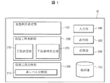
【解決手段】ナノ素子の設計のための仮想実験物質を決定する仮想試片決定部100と、仮想試片決定部で決定された仮想実験物質に一つ以上の工程を適用する仮想工程実験部200、および仮想工程実験部で仮想実験物質に適用されたそれぞれの工程結果を分析する仮想工程分析部300と、を含む、ナノ素子設計用仮想実験装置10を含む。仮想工程分析部は、工程結果を、一つ以上の粒子レベルを基準として分析する多レベル分析部をさらに含む。
【選択図】図1
Description
100 仮想試片決定部
200 仮想工程実験部
210 工程決定部
220 工程条件決定部
300 仮想工程分析部
310 多レベル分析部
400 入力部
500 表示部
600 通信部
700 格納部
Claims (18)
- ナノ素子の設計のための仮想実験物質を決定する仮想試片決定部と、
前記仮想試片決定部で決定された仮想実験物質に一つ以上の工程を適用する仮想工程実験部と、
前記仮想工程実験部で前記仮想実験物質に適用されたそれぞれの工程結果を分析する仮想工程分析部と、
を含む、ナノ素子設計用仮想実験装置。 - 前記仮想工程分析部は、前記工程結果を、一つ以上の粒子レベルを基準として分析する多レベル分析部をさらに含む、請求項1に記載のナノ素子設計用仮想実験装置。
- 前記多レベル分析部は、前記工程結果を量子力学計算に基づいた電子レベル、原子間のポテンシャルを用いて古典力学的計算を行う分子レベル、および連続体レベルで分析する、請求項2に記載のナノ素子設計用仮想実験装置。
- 前記仮想工程実験部は、前記仮想実験物質に適用する一つ以上の工程の種類、回数、または順序を決定する工程決定部をさらに含む、請求項1または2に記載のナノ素子設計用仮想実験装置。
- 前記仮想工程実験部は、前記仮想実験物質に適用する一つ以上の工程条件を変更する工程条件決定部をさらに含む、請求項1または2に記載のナノ素子設計用仮想実験装置。
- 前記仮想試片決定部は、
仮想実験物質のうちのウェハー基板の材料、初期厚さ、結晶方向、または初期ドーピング、
実験領域の大きさおよび位置、
メッシュ(mesh)のレゾリューション(resolution)および特性、
のうちの少なくともいずれか一つを決定する、請求項1に記載のナノ素子設計用仮想実験装置。 - 前記工程は、アニーリング、酸化、拡散、蒸着、注入(Implantation)、露光、エッチング、CMP(Chemical Mechanical Planarization)、ALD(atomic layer deposition)、スパッタリングのうちのいずれか一つである、請求項1に記載のナノ素子設計用仮想実験装置。
- 前記工程条件は、温度、圧力、不純物調節のうちのいずれか一つである、請求項5に記載のナノ素子設計用仮想実験装置。
- 前記仮想工程分析部は、電子構造、電流−電圧分布、原子力電子顕微鏡(Atomic−Force Microscope、AFM)、RDF、ストレス(Stress)を分析する、請求項1に記載のナノ素子設計用仮想実験装置。
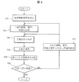
- ナノ素子の設計のための仮想実験物質を決定する段階と、
前記決定された仮想実験物質に一つ以上の工程を適用する段階と、
前記仮想実験物質に適用されたそれぞれの工程結果を分析する段階と、
を含む、ナノ素子の設計のための仮想実験方法。 - 前記工程結果を分析する段階は、前記工程結果を、一つ以上の粒子レベルを基準として分析する段階をさらに含む、請求項10に記載のナノ素子の設計のための仮想実験方法。
- 前記粒子レベルを基準として分析する段階は、前記工程結果を電子レベル、分子レベル、および連続体レベルで分析する、請求項11に記載のナノ素子の設計のための仮想実験方法。
- 前記一つ以上の工程を適用する段階は、前記仮想実験物質に適用する一つ以上の工程の種類、回数、または順序を決定する段階をさらに含む、請求項10または11に記載のナノ素子の設計のための仮想実験方法。
- 前記一つ以上の工程を適用する段階は、前記仮想実験物質に適用する一つ以上の工程条件を決定する段階をさらに含む、請求項10または11に記載のナノ素子の設計のための仮想実験方法。
- 前記仮想実験物質を決定する段階は、
仮想実験物質のうちのウェハー基板の材料、初期厚さ、結晶方向、または初期ドーピング、
実験領域の大きさおよび位置、
メッシュ(mesh)のレゾリューション(resolution)および特性、
のうちの少なくともいずれか一つを決定する段階をさらに含む、請求項10に記載のナノ素子の設計のための仮想実験方法。 - 前記工程は、アニーリング、酸化、拡散、蒸着、注入(Implantation)、露光、エッチング、CMP(Chemical Mechanical Planarization)、ALD(atomic layer deposition)、スパッタリング(Sputtering)のうちのいずれか一つである、請求項10に記載のナノ素子の設計のための仮想実験方法。
- 前記工程条件は、温度、圧力、不純物調節のうちの一つである、請求項14に記載のナノ素子の設計のための仮想実験方法。
- 前記仮想実験物質を決定する段階は、電子構造、電流−電圧分布、原子力電子顕微鏡(Atomic−Force Microscope、AFM)、RDF、ストレス(stress)を分析する段階をさらに含む、請求項10に記載のナノ素子の設計のための仮想実験方法。
Applications Claiming Priority (2)
| Application Number | Priority Date | Filing Date | Title |
|---|---|---|---|
| KR1020120150554A KR101474331B1 (ko) | 2012-12-21 | 2012-12-21 | 나노 소자 설계용 다차원 가상 실험 장치 및 그 방법 |
| KR10-2012-0150554 | 2012-12-21 |
Publications (1)
| Publication Number | Publication Date |
|---|---|
| JP2014123735A true JP2014123735A (ja) | 2014-07-03 |
Family
ID=50112657
Family Applications (1)
| Application Number | Title | Priority Date | Filing Date |
|---|---|---|---|
| JP2013262911A Pending JP2014123735A (ja) | 2012-12-21 | 2013-12-19 | ナノ素子設計用仮想実験装置およびナノ素子の設計のための仮想実験方法 |
Country Status (4)
| Country | Link |
|---|---|
| US (1) | US20140180645A1 (ja) |
| EP (1) | EP2746974A3 (ja) |
| JP (1) | JP2014123735A (ja) |
| KR (1) | KR101474331B1 (ja) |
Cited By (1)
| Publication number | Priority date | Publication date | Assignee | Title |
|---|---|---|---|---|
| JP2024529329A (ja) * | 2021-07-22 | 2024-08-06 | シージェイ チェルジェダン コーポレイション | テンプレートベースの結晶化工程モデル生成装置およびその方法 |
Families Citing this family (9)
| Publication number | Priority date | Publication date | Assignee | Title |
|---|---|---|---|---|
| WO2015048509A1 (en) | 2013-09-26 | 2015-04-02 | Synopsys, Inc. | First principles design automation tool |
| US10489212B2 (en) | 2013-09-26 | 2019-11-26 | Synopsys, Inc. | Adaptive parallelization for multi-scale simulation |
| US20160162625A1 (en) | 2013-09-26 | 2016-06-09 | Synopsys, Inc. | Mapping Intermediate Material Properties To Target Properties To Screen Materials |
| US10417373B2 (en) | 2013-09-26 | 2019-09-17 | Synopsys, Inc. | Estimation of effective channel length for FinFETs and nano-wires |
| US10516725B2 (en) | 2013-09-26 | 2019-12-24 | Synopsys, Inc. | Characterizing target material properties based on properties of similar materials |
| US9836563B2 (en) | 2013-09-26 | 2017-12-05 | Synopsys, Inc. | Iterative simulation with DFT and non-DFT |
| KR102208433B1 (ko) * | 2014-08-21 | 2021-01-27 | 삼성전자주식회사 | 적어도 하나 이상의 통신 방식을 선택하기 위한 방법 및 장치 |
| US10078735B2 (en) | 2015-10-30 | 2018-09-18 | Synopsys, Inc. | Atomic structure optimization |
| US10734097B2 (en) | 2015-10-30 | 2020-08-04 | Synopsys, Inc. | Atomic structure optimization |
Citations (10)
| Publication number | Priority date | Publication date | Assignee | Title |
|---|---|---|---|---|
| JPH05267421A (ja) * | 1992-03-17 | 1993-10-15 | Hitachi Ltd | 半導体デバイスシミュレーション方法 |
| JPH09306967A (ja) * | 1996-05-16 | 1997-11-28 | Ricoh Co Ltd | 半導体シミュレーション装置および半導体シミュレーション方法 |
| JP2001185713A (ja) * | 1999-12-22 | 2001-07-06 | Nec Corp | デバイスシミュレーション方法 |
| JP2005340340A (ja) * | 2004-05-25 | 2005-12-08 | Renesas Technology Corp | 半導体シミュレーション装置および半導体シミュレーション方法 |
| JP2007103919A (ja) * | 2005-09-07 | 2007-04-19 | Seiko Epson Corp | シミュレーション装置、シミュレーション方法、シミュレーションプログラム、記録媒体、及び半導体装置 |
| JP2007134574A (ja) * | 2005-11-11 | 2007-05-31 | Canon Inc | シミュレーション方法及びその装置、プログラム、記憶媒体 |
| WO2008015835A1 (en) * | 2006-08-01 | 2008-02-07 | Nec Corporation | Method, device, and program for simulating nano-substance in electric field |
| WO2008075642A1 (ja) * | 2006-12-18 | 2008-06-26 | Nec Corporation | 半導体装置及びその製造方法 |
| JP2011192787A (ja) * | 2010-03-15 | 2011-09-29 | Toshiba Corp | 半導体記憶装置 |
| JP2011211127A (ja) * | 2010-03-31 | 2011-10-20 | Tokyo Institute Of Technology | ナノワイヤトランジスタ及びその製造方法 |
Family Cites Families (2)
| Publication number | Priority date | Publication date | Assignee | Title |
|---|---|---|---|---|
| JP2000195766A (ja) * | 1998-12-25 | 2000-07-14 | Toshiba Corp | シミュレ―ション装置、シミュレ―ション方法、シミュレ―ションプログラムを格納した記録媒体および固体電子装置の製造方法 |
| JP4047581B2 (ja) | 2001-12-12 | 2008-02-13 | 社団法人化学工学会 | 材料設計支援方法ならびにそのシステム |
-
2012
- 2012-12-21 KR KR1020120150554A patent/KR101474331B1/ko not_active Expired - Fee Related
-
2013
- 2013-12-11 US US14/103,165 patent/US20140180645A1/en not_active Abandoned
- 2013-12-12 EP EP13196981.8A patent/EP2746974A3/en not_active Withdrawn
- 2013-12-19 JP JP2013262911A patent/JP2014123735A/ja active Pending
Patent Citations (10)
| Publication number | Priority date | Publication date | Assignee | Title |
|---|---|---|---|---|
| JPH05267421A (ja) * | 1992-03-17 | 1993-10-15 | Hitachi Ltd | 半導体デバイスシミュレーション方法 |
| JPH09306967A (ja) * | 1996-05-16 | 1997-11-28 | Ricoh Co Ltd | 半導体シミュレーション装置および半導体シミュレーション方法 |
| JP2001185713A (ja) * | 1999-12-22 | 2001-07-06 | Nec Corp | デバイスシミュレーション方法 |
| JP2005340340A (ja) * | 2004-05-25 | 2005-12-08 | Renesas Technology Corp | 半導体シミュレーション装置および半導体シミュレーション方法 |
| JP2007103919A (ja) * | 2005-09-07 | 2007-04-19 | Seiko Epson Corp | シミュレーション装置、シミュレーション方法、シミュレーションプログラム、記録媒体、及び半導体装置 |
| JP2007134574A (ja) * | 2005-11-11 | 2007-05-31 | Canon Inc | シミュレーション方法及びその装置、プログラム、記憶媒体 |
| WO2008015835A1 (en) * | 2006-08-01 | 2008-02-07 | Nec Corporation | Method, device, and program for simulating nano-substance in electric field |
| WO2008075642A1 (ja) * | 2006-12-18 | 2008-06-26 | Nec Corporation | 半導体装置及びその製造方法 |
| JP2011192787A (ja) * | 2010-03-15 | 2011-09-29 | Toshiba Corp | 半導体記憶装置 |
| JP2011211127A (ja) * | 2010-03-31 | 2011-10-20 | Tokyo Institute Of Technology | ナノワイヤトランジスタ及びその製造方法 |
Cited By (2)
| Publication number | Priority date | Publication date | Assignee | Title |
|---|---|---|---|---|
| JP2024529329A (ja) * | 2021-07-22 | 2024-08-06 | シージェイ チェルジェダン コーポレイション | テンプレートベースの結晶化工程モデル生成装置およびその方法 |
| JP7635462B2 (ja) | 2021-07-22 | 2025-02-25 | シージェイ チェルジェダン コーポレイション | テンプレートベースの結晶化工程モデル生成装置およびその方法 |
Also Published As
| Publication number | Publication date |
|---|---|
| US20140180645A1 (en) | 2014-06-26 |
| EP2746974A3 (en) | 2017-08-09 |
| EP2746974A2 (en) | 2014-06-25 |
| KR20140091086A (ko) | 2014-07-21 |
| KR101474331B1 (ko) | 2014-12-18 |
Similar Documents
| Publication | Publication Date | Title |
|---|---|---|
| KR101474331B1 (ko) | 나노 소자 설계용 다차원 가상 실험 장치 및 그 방법 | |
| Smidstrup et al. | QuantumATK: an integrated platform of electronic and atomic-scale modelling tools | |
| Chang et al. | Design rules for self-assembled block copolymer patterns using tiled templates | |
| Wang et al. | Experimental realization of an extended Fermi-Hubbard model using a 2D lattice of dopant-based quantum dots | |
| Jeong et al. | Bridging TCAD and AI: Its application to semiconductor design | |
| Braatz et al. | Perspectives on the design and control of multiscale systems | |
| Maassen et al. | Quantum transport modeling from first principles | |
| Wolkow et al. | Silicon atomic quantum dots enable beyond-CMOS electronics | |
| Walter et al. | Hexagons are the bestagons: design automation for silicon dangling bond logic | |
| Wagner | Quantum Monte Carlo for Ab Initio calculations of energy‐relevant materials | |
| Weitzer et al. | Expanding FEBID-Based 3D-Nanoprinting toward Closed High-Fidelity Nanoarchitectures | |
| Spetzler et al. | The role of vacancy dynamics in two‐dimensional memristive devices | |
| Stuyck et al. | CMOS compatibility of semiconductor spin qubits | |
| WO2005103944A1 (en) | A nano molecular modeling method | |
| Hwang et al. | Giant renormalization of dopant impurity levels in 2D semiconductor MoS2 | |
| Han et al. | Acceleration of three-dimensional device simulation with the 3D convolutional neural network | |
| JPWO2008015835A1 (ja) | 電界下のナノ物質シミュレーション方法と装置並びにプログラム | |
| Tang et al. | Deep-learning electronic structure calculations | |
| Hasan et al. | beyond the surface—exploring the complexities of 2D materials with density functional theory | |
| Yam et al. | A multi-scale modeling of junctionless field-effect transistors | |
| Glavin et al. | Quantum materials manufacturing | |
| Macucci et al. | Status and perspectives of nanoscale device modelling | |
| Mittal et al. | Using energy landscapes to predict the properties of thin films | |
| Boero et al. | First-principles molecular dynamics methods: an overview | |
| Song et al. | One-dimensional topological phase and tunable soliton states in atomic nanolines on Si (001) surface |
Legal Events
| Date | Code | Title | Description |
|---|---|---|---|
| A131 | Notification of reasons for refusal |
Free format text: JAPANESE INTERMEDIATE CODE: A131 Effective date: 20150210 |
|
| A521 | Request for written amendment filed |
Free format text: JAPANESE INTERMEDIATE CODE: A523 Effective date: 20150428 |
|
| A131 | Notification of reasons for refusal |
Free format text: JAPANESE INTERMEDIATE CODE: A131 Effective date: 20150825 |
|
| A521 | Request for written amendment filed |
Free format text: JAPANESE INTERMEDIATE CODE: A523 Effective date: 20151125 |
|
| A02 | Decision of refusal |
Free format text: JAPANESE INTERMEDIATE CODE: A02 Effective date: 20160209 |