JP2014107594A - Image pick-up device and imaging apparatus - Google Patents
Image pick-up device and imaging apparatus Download PDFInfo
- Publication number
- JP2014107594A JP2014107594A JP2012256839A JP2012256839A JP2014107594A JP 2014107594 A JP2014107594 A JP 2014107594A JP 2012256839 A JP2012256839 A JP 2012256839A JP 2012256839 A JP2012256839 A JP 2012256839A JP 2014107594 A JP2014107594 A JP 2014107594A
- Authority
- JP
- Japan
- Prior art keywords
- pixel
- parallax
- image
- opening
- width
- Prior art date
- Legal status (The legal status is an assumption and is not a legal conclusion. Google has not performed a legal analysis and makes no representation as to the accuracy of the status listed.)
- Pending
Links
Images


Abstract
Description
本発明は、撮像素子および撮像装置に関する。 The present invention relates to an imaging element and an imaging apparatus.
単一の撮影光学系を用いて、互いに視差を有する左右の視差画像を一度の撮影で生成する撮像装置が知られている。当該撮像装置においては、撮像素子に配列された全ての画素の右半分または左半分は遮光部材により遮光されている。
[先行技術文献]
[特許文献]
[特許文献1] 特開2003−7994号公報
[特許文献2] 特開2011−197278号公報
2. Description of the Related Art There is known an imaging apparatus that generates left and right parallax images having parallax with a single shooting using a single shooting optical system. In the imaging apparatus, the right half or the left half of all the pixels arranged in the imaging element is shielded from light by the light shielding member.
[Prior art documents]
[Patent Literature]
[Patent Document 1] JP 2003-7994 A [Patent Document 2] JP 2011-197278 A
撮像素子は、遮光部材により遮光されている画素(視差画素)に加えて、遮光部材により遮光されていない画素(視差なし画素)を含む場合がある。左右に視差を生じさせる場合には、視差画素においては、遮光部材により制限された入射光束を受光する受光領域の水平方向の幅は、垂直方向の幅より短い場合が多い。一方、視差なし画素においては、遮光部材により制限されていない入射光束を受光する受光領域の水平方向の幅は、垂直方向の幅と同一である場合が多い。このように視差画素と視差なし画素とで受光領域の形状が異なる場合には、左右の視差画像と視差なし画像とでボケの出かたが異なるという問題がある。 The imaging device may include pixels (non-parallax pixels) that are not shielded by the light shielding member in addition to pixels (parallax pixels) that are shielded by the light shielding member. When parallax is generated on the left and right, in the parallax pixels, the horizontal width of the light receiving region that receives the incident light beam limited by the light blocking member is often shorter than the vertical width. On the other hand, in non-parallax pixels, the horizontal width of the light receiving region that receives an incident light beam that is not limited by the light shielding member is often the same as the vertical width. As described above, when the shape of the light receiving region is different between the parallax pixel and the non-parallax pixel, there is a problem that the blurring is different between the left and right parallax images and the non-parallax image.
本発明の第1の態様における撮像素子は、1つの光学系の入射光束に対して、基準方向の視点を生み出す開口マスクを備えた視差なし画素と、左方向の視点を生み出す開口マスクを備えた左視差画素と、右方向の視点を生み出す開口マスクを備えた右視差画素の少なくとも3種類の画素を持つ画素配列からなる撮像素子であって、視差なし画素の開口マスクの垂直開口幅が水平開口幅より狭い。 The imaging device according to the first aspect of the present invention includes a non-parallax pixel including an aperture mask that generates a viewpoint in the reference direction and an aperture mask that generates a viewpoint in the left direction with respect to an incident light beam of one optical system. An imaging device comprising a pixel array having at least three types of pixels, that is, a left parallax pixel and a right parallax pixel having an aperture mask that generates a right viewpoint, and a vertical aperture width of an aperture mask of a pixel with no parallax is a horizontal aperture Narrower than width.
本発明の第2の態様における撮像素子は、1つの光学系の入射光束に対して、基準方向の視点を生み出すマイクロレンズと開口マスクを備えた視差なし画素と、左方向の視点を生み出すマイクロレンズと開口マスクを備えた左視差画素と、右方向の視点を生み出すマイクロレンズと開口マスクを備えた右視差画素の少なくとも3種類の画素を持つ画素配列からなる撮像素子であって、視差なし画素のマイクロレンズの集光特性を垂直方向が水平方向より少なくなるように非等方な形に変形する。 The imaging device according to the second aspect of the present invention includes a microlens that generates a viewpoint in a reference direction and a non-parallax pixel including an aperture mask, and a microlens that generates a viewpoint in the left direction with respect to an incident light beam of one optical system. And an imaging device having a pixel array having at least three types of pixels: a left parallax pixel having an aperture mask, a microlens that generates a right viewpoint, and a right parallax pixel having an aperture mask. The condensing characteristic of the microlens is deformed into an anisotropic shape so that the vertical direction is less than the horizontal direction.
本発明の第3の態様における撮像装置は、上記の撮像素子と、光路途中に円形の絞りを備える1つの光学系とを備える。 An imaging device according to a third aspect of the present invention includes the above-described imaging device and one optical system including a circular diaphragm in the middle of the optical path.
本発明の第4の態様における撮像素子は、被写体光束を受光する第1受光領域が、画素中心に対して第1軸方向に偏位した位置に設定された偏位画素と、被写体光束を受光する第2受光領域が、画素中心に対して偏位していない位置に設定された非偏位画素とを備え、第1受光領域における第1軸方向の第1領域幅は、第1軸方向に直交する第2軸方向の第2領域幅よりも短く、第2受光領域における第1軸方向の第1領域幅は、第2軸方向の第2領域幅より長い。 The imaging device according to the fourth aspect of the present invention receives a deviated pixel in which a first light receiving region for receiving a subject luminous flux is set at a position displaced in the first axis direction with respect to the pixel center, and the subject luminous flux. The second light receiving area includes non-deviation pixels set at positions not deviated with respect to the pixel center, and the first area width in the first axis direction of the first light receiving area is the first axis direction. The first region width in the first axis direction in the second light receiving region is longer than the second region width in the second axis direction.
本発明の第5の態様における撮像素子は、第1マイクロレンズにより集光された被写体光束を受光する第1受光領域が、画素中心に対して第1軸方向に偏位した位置に設定された偏位画素と、第2マイクロレンズにより集光された被写体光束を受光する第2受光領域が、画素中心に対して偏位していない位置に設定された非偏位画素とを備え、第1受光領域における第1軸方向の第1領域幅は、第1軸方向に直交する第2軸方向の第2領域幅よりも短く、第2マイクロレンズの第1軸方向に対応する方向の入射光量は、第1軸方向に直交する第2軸方向に対応する方向の入射光量より多い。 In the imaging device according to the fifth aspect of the present invention, the first light receiving region for receiving the subject light beam condensed by the first microlens is set at a position displaced in the first axis direction with respect to the pixel center. A displacement pixel, and a second light-receiving region that receives the subject light beam collected by the second microlens is provided with a non-deviation pixel that is set at a position that is not displaced with respect to the pixel center. The first region width in the first axis direction in the light receiving region is shorter than the second region width in the second axis direction orthogonal to the first axis direction, and the incident light amount in the direction corresponding to the first axis direction of the second microlens. Is greater than the amount of incident light in the direction corresponding to the second axis direction orthogonal to the first axis direction.
本発明の第6の態様における撮像装置は、上記の撮像素子と、撮像素子に導く被写体光束を調整する円形絞りを有する1つの光学系とを備える。 An image pickup apparatus according to a sixth aspect of the present invention includes the above-described image pickup element and one optical system having a circular diaphragm that adjusts a subject light beam guided to the image pickup element.
以下、発明の実施の形態を通じて本発明を説明するが、以下の実施形態は特許請求の範囲にかかる発明を限定するものではない。また、実施形態の中で説明されている特徴の組み合わせの全てが発明の解決手段に必須であるとは限らない。 Hereinafter, the present invention will be described through embodiments of the invention, but the following embodiments do not limit the invention according to the claims. In addition, not all the combinations of features described in the embodiments are essential for the solving means of the invention.
撮像装置の一形態である本実施形態に係るデジタルカメラは、1つのシーンについて複数の視点数の画像を一度の撮影により生成できるように構成されている。互いに視点の異なるそれぞれの画像を視差画像と呼ぶ。本実施形態においては、特に、右目と左目に対応する2つの視点による右視差画像と左視差画像を生成する場合について説明する。本実施形態におけるデジタルカメラは、基準方向の視点として中央視点による視差のない視差なし画像も、視差画像と共に生成できる。 The digital camera according to the present embodiment, which is one form of the imaging device, is configured to generate images with a plurality of viewpoints for one scene by one shooting. Each image having a different viewpoint is called a parallax image. In the present embodiment, a case where a right parallax image and a left parallax image from two viewpoints corresponding to the right eye and the left eye are generated will be described. The digital camera according to the present embodiment can generate a parallax-free image with no parallax from the central viewpoint as the viewpoint in the reference direction together with the parallax image.
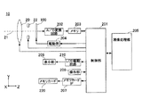
図1は、本発明の実施形態に係るデジタルカメラ10の構成を説明する図である。デジタルカメラ10は、撮影光学系としての撮影レンズ20を備え、光軸21に沿って入射する被写体光束を撮像素子100へ導く。撮影レンズ20は、デジタルカメラ10に対して着脱できる交換式レンズであっても構わない。デジタルカメラ10は、撮像素子100、制御部201、A/D変換回路202、メモリ203、駆動部204、画像処理部205、メモリカードIF207、操作部208、表示部209およびLCD駆動回路210を備える。
FIG. 1 is a diagram illustrating the configuration of a
なお、図示するように、撮像素子100へ向かう光軸21に平行な方向をZ軸プラス方向と定め、Z軸と直交する平面において紙面手前へ向かう方向をX軸プラス方向、紙面上方向をY軸プラス方向と定める。以降のいくつかの図においては、図1の座標軸を基準として、それぞれの図の向きがわかるように座標軸を表示する。
As shown in the figure, the direction parallel to the
撮影レンズ20は、複数の光学レンズ群から構成され、シーンからの被写体光束をその焦点面近傍に結像させる。なお、図1では撮影レンズ20を説明の都合上、瞳近傍に配置された仮想的な1枚のレンズで代表して表している。絞り22は円形絞りであり、光軸21に沿って瞳近傍に配置されている。
The taking
撮像素子100は、撮影レンズ20の焦点面近傍に配置されている。撮像素子100は、二次元的に複数の光電変換素子が配列された、例えばCCD、CMOSセンサ等のイメージセンサである。撮像素子100は、駆動部204によりタイミング制御されて、受光面上に結像された被写体像を画像信号に変換してA/D変換回路202へ出力する。また、撮像素子100は、視差画素と視差なし画素を含む。視差画素は、被写体光束を受光する受光領域が画素中心に対してX軸方向に偏位した位置に設定される画素である。受光領域が偏位している点に着目すると、視差画素を偏位画素ということもできる。一方、視差なし画素は、受光領域が画素中心に対して偏位していない位置に設定される画素である。受光領域が偏位していない点に着目すると、視差なし画素を非偏位画素ということもできる。なお、左視点の視差画素を視差Lt画素、右視点の視差画素を視差Rt画素、視差なし画素をN画素と記す場合もある。また、左視点の視差画像を視差Lt画像、右視点の視差画像を視差Rt画像、視差なし画像をN画像と記す場合もある。
The
A/D変換回路202は、撮像素子100が出力する画像信号をデジタル画像信号に変換してメモリ203へ出力する。画像処理部205は、メモリ203をワークスペースとして種々の画像処理を施し、画像データを生成する。
The A /
画像処理部205は、他にも選択された画像フォーマットにしたがって画像データを調整するなどの画像処理一般の機能も担う。生成された画像データは、LCD駆動回路210により表示信号に変換され、表示部209に表示される。また、メモリカードIF207に装着されているメモリカード220に記録される。
The
制御部201は、デジタルカメラ10を統合的に制御する。例えば、設定された絞り値に応じて絞り22の開口を調整し、AF評価値に応じて撮影レンズ20を光軸方向に進退させる。また、撮影レンズ20の位置を検出して、撮影レンズ20の焦点距離、フォーカスレンズ位置を把握する。さらに、駆動部204に対してタイミング制御信号を送信し、撮像素子100から出力される画像信号が画像処理部205で画像データに処理されるまでの一連の撮像制御を管理する。
The
操作部208は、ユーザの操作を受け付けて制御部201へ指示を伝達する受付部の一部として機能する。操作部208は、撮影開始指示を受け付けるシャッタボタン等、複数の操作部材を含む。
The
<視差画素とボケ特性>
次に、視差Lt画素および視差Rt画素が受光する場合のデフォーカスの概念を説明する。まず、視差なし画素におけるデフォーカスの概念について簡単に説明する図である。図2は、視差なし画素におけるデフォーカスの概念を説明する図である。図2(a)で示すように、被写体である物点が焦点位置に存在する場合、レンズ瞳を通って撮像素子受光面に到達する被写体光束は、対応する像点の画素を中心として急峻な光強度分布を示す。すなわち、レンズ瞳を通過する有効光束の全体を受光する視差なし画素が像点近傍に配列されていれば、像点に対応する画素の出力値が最も大きく、周辺に配列された画素の出力値は急激に低下する。
<Parallax pixel and blur characteristics>
Next, the concept of defocusing when the parallax Lt pixel and the parallax Rt pixel receive light will be described. First, it is a figure explaining simply the concept of defocus in a pixel without parallax. FIG. 2 is a diagram for explaining the concept of defocusing in a non-parallax pixel. As shown in FIG. 2A, when an object point that is a subject exists at the focal position, the subject luminous flux that reaches the image sensor light receiving surface through the lens pupil is steep with the pixel at the corresponding image point as the center. The light intensity distribution is shown. That is, if non-parallax pixels that receive the entire effective luminous flux that passes through the lens pupil are arranged in the vicinity of the image point, the output value of the pixel corresponding to the image point is the largest, and the output value of the pixels arranged in the vicinity Drops rapidly.
一方、図2(b)に示すように、撮像素子受光面から遠ざかる方向に、物点が焦点位置からずれると、被写体光束は、物点が焦点位置に存在する場合に比べて、撮像素子受光面においてなだらかな光強度分布を示す。すなわち、対応する像点の画素における出力値が低下する上に、より周辺画素まで出力値を有する分布を示す。 On the other hand, as shown in FIG. 2B, when the object point deviates from the focal position in the direction away from the light receiving surface of the image sensor, the subject luminous flux is received by the image sensor compared to the case where the object point exists at the focus position. It shows a gentle light intensity distribution on the surface. That is, the output value at the pixel of the corresponding image point is lowered, and a distribution having output values up to the peripheral pixels is shown.
図2(c)に示すように、さらに物点が焦点位置からずれると、被写体光束は、撮像素子受光面においてよりなだらかな光強度分布を示す。すなわち、対応する像点の画素における出力値がさらに低下する上に、より周辺画素まで出力値を有する分布を示す。 As shown in FIG. 2C, when the object point further deviates from the focal position, the subject luminous flux exhibits a gentler light intensity distribution on the image sensor light receiving surface. In other words, the output value at the pixel of the corresponding image point further decreases, and a distribution having output values up to the surrounding pixels is shown.
図2(d)に示すように、撮像素子受光面に近づく方向に、物点が焦点位置からずれた場合にも、撮像素子受光面から遠ざかる方向に物点がずれた場合と同じような光強度分布を示す。 As shown in FIG. 2D, when the object point is shifted from the focal position in the direction approaching the image sensor light receiving surface, the same light as when the object point is shifted in the direction away from the image sensor light receiving surface. The intensity distribution is shown.
図3は、視差画素におけるデフォーカスの概念を説明する図である。視差Lt画素および視差Rt画素は、レンズ瞳の部分領域としてそれぞれ光軸対象に設定された2つの視差仮想瞳のいずれかから到達する被写体光束を受光する。本明細書において、単一のレンズ瞳における互いに異なる仮想瞳から到達する被写体光束を受光することによって視差画像を撮像する方式を単眼瞳分割撮像方式という。 FIG. 3 is a diagram for explaining the concept of defocusing in the parallax pixels. The parallax Lt pixel and the parallax Rt pixel receive the subject luminous flux that arrives from one of the two parallax virtual pupils set as the optical axis target as a partial region of the lens pupil. In this specification, a method of capturing a parallax image by receiving subject light fluxes that arrive from different virtual pupils in a single lens pupil is referred to as a monocular pupil division imaging method.
図3(a)で示すように、被写体である物点が焦点位置に存在する場合、いずれの視差仮想瞳を通った被写体光束であっても、対応する像点の画素を中心として急峻な光強度分布を示す。像点付近に視差Lt画素が配列されていれば、像点に対応する画素の出力値が最も大きく、周辺に配列された画素の出力値が急激に低下する。また、像点付近に視差Rt画素が配列されていても、像点に対応する画素の出力値が最も大きく、周辺に配列された画素の出力値が急激に低下する。すなわち、被写体光束がいずれの視差仮想瞳を通過しても、像点に対応する画素の出力値が最も大きく、周辺に配列された画素の出力値が急激に低下する分布を示し、それぞれの分布は互いに一致する。 As shown in FIG. 3 (a), when an object point that is a subject exists at the focal position, steep light centering on the pixel of the corresponding image point, regardless of the parallax virtual pupil, regardless of the parallax virtual pupil. The intensity distribution is shown. If the parallax Lt pixels are arranged in the vicinity of the image point, the output value of the pixel corresponding to the image point is the largest, and the output value of the pixels arranged in the vicinity rapidly decreases. Further, even when the parallax Rt pixels are arranged in the vicinity of the image point, the output value of the pixel corresponding to the image point is the largest, and the output value of the pixels arranged in the vicinity rapidly decreases. That is, even if the subject luminous flux passes through any parallax virtual pupil, the output value of the pixel corresponding to the image point is the largest, and the output value of the pixels arranged in the vicinity rapidly decreases. Match each other.
一方、図3(b)に示すように、撮像素子受光面から遠ざかる方向に、物点が焦点位置からずれると、物点が焦点位置に存在した場合に比べて、視差Lt画素が示す光強度分布のピークは、像点に対応する画素から一方向に離れた位置に現れ、かつその出力値は低下する。また、出力値を有する画素の幅も広がる。すなわち、撮像素子受光面の水平方向に対して点像の広がりを有することになるので、ボケ量は増す。視差Rt画素が示す光強度分布のピークは、像点に対応する画素から、視差Lt画素における一方向とは逆向きかつ等距離に離れた位置に現れ、同様にその出力値は低下する。また、同様に出力値を有する画素の幅も広がる。すなわち、物点が焦点位置に存在した場合に比べてなだらかとなった同一の光強度分布が、互いに等距離に離間して現れる。視差Lt画素および視差Rt画素が示す光強度分布のピーク間のずれ量は、視差量に相当する。 On the other hand, as shown in FIG. 3B, when the object point deviates from the focal position in the direction away from the light receiving surface of the image sensor, the light intensity indicated by the parallax Lt pixel is greater than when the object point exists at the focal position. The distribution peak appears at a position away from the pixel corresponding to the image point in one direction, and its output value decreases. In addition, the width of the pixel having the output value is increased. That is, since the point image spreads in the horizontal direction of the light receiving surface of the image sensor, the amount of blur increases. The peak of the light intensity distribution indicated by the parallax Rt pixel appears at a position away from the pixel corresponding to the image point in the opposite direction to the one direction in the parallax Lt pixel and at an equal distance, and the output value similarly decreases. Similarly, the width of the pixel having the output value is increased. That is, the same light intensity distribution that is gentler than that in the case where the object point exists at the focal position appears at an equal distance from each other. The shift amount between the peaks of the light intensity distribution indicated by the parallax Lt pixel and the parallax Rt pixel corresponds to the parallax amount.
また、図3(c)に示すように、さらに物点が焦点位置からずれると、図3(b)の状態に比べて、さらになだらかとなった同一の光強度分布が、より離間して現れる。点像の広がりがより大きくなるので、ボケ量は増す。また、視差Lt画素および視差Rt画素が示す光強度分布のピーク間のずれも大きくなっているので、視差量も増す。つまり、物点が焦点位置から大きくずれる程、ボケ量と視差量が増すと言える。 Further, as shown in FIG. 3C, when the object point further deviates from the focal position, the same light intensity distribution that is more gentle than the state of FIG. 3B appears further apart. . Since the spread of the point image becomes larger, the amount of blur increases. In addition, since the deviation between the peaks of the light intensity distribution indicated by the parallax Lt pixel and the parallax Rt pixel is large, the parallax amount is also increased. In other words, it can be said that the more the object point deviates from the focal position, the more the amount of blur and the amount of parallax increase.
図3(d)に示すように、撮像素子受光面に近づく方向に、物点が焦点位置からずれた場合には、図3(c)の状態とは逆に、視差Rt画素が示す光強度分布のピークは、像点に対応する画素から上記一方向に離れた位置に現れる。視差Lt画素が示す光強度分布のピークは、視差Rt画素における一方向とは逆向きに離れた位置に現れる。すなわち、物点のずれの方向に応じて、視差Lt画素および視差Rt画素が示す光強度分布のピークが、像点に対応する画素からどちらの方向に離れた位置に現れるかが決まる。 As shown in FIG. 3D, when the object point deviates from the focal position in the direction approaching the light receiving surface of the image sensor, the light intensity indicated by the parallax Rt pixel is opposite to the state of FIG. The distribution peak appears at a position away from the pixel corresponding to the image point in the one direction. The peak of the light intensity distribution indicated by the parallax Lt pixel appears at a position away from the one direction in the parallax Rt pixel. That is, it is determined in which direction the peak of the light intensity distribution indicated by the parallax Lt pixel and the parallax Rt pixel appears in the direction away from the pixel corresponding to the image point according to the direction of deviation of the object point.
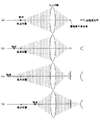
図2で説明した光強度分布の変化と、図3で説明した光強度分布の変化をそれぞれグラフ化すると、図4のように表される。図4は、視差なし画素と視差画素の光強度分布を示す図である。図において、横軸は画素位置を表し、中心位置が像点に対応する画素位置である。縦軸は各画素の出力値を表し、この出力値は実質的に光強度に比例するので、図においては光強度として示す。 When the change of the light intensity distribution explained in FIG. 2 and the change of the light intensity distribution explained in FIG. 3 are respectively graphed, they are expressed as shown in FIG. FIG. 4 is a diagram illustrating the light intensity distribution of the non-parallax pixel and the parallax pixel. In the figure, the horizontal axis represents the pixel position, and the center position is the pixel position corresponding to the image point. The vertical axis represents the output value of each pixel. Since this output value is substantially proportional to the light intensity, it is shown as the light intensity in the figure.
なお、上述のように、撮像素子受光面に近づく方向に、物点が焦点位置からずれた場合も、撮像素子受光面から遠ざかる方向に物点がずれた場合と同じような光強度分布を示すので、図において、撮像素子受光面に近づく方向にずれた場合の光強度分布の変化を省略している。撮像素子受光面に近づく方向に、物点が焦点位置からずれた場合の視差Lt画素および視差Rt画素が示す光強度分布のピークについても、撮像素子受光面から遠ざかる方向に物点がずれた場合の視差Lt画素および視差Rt画素が示す光強度分布のピークと同様であるので、省略している。 As described above, when the object point deviates from the focal position in the direction approaching the image sensor light receiving surface, the same light intensity distribution as when the object point deviates in the direction away from the image sensor light receiving surface is shown. Therefore, in the figure, the change in the light intensity distribution when the image sensor is shifted in the direction approaching the light receiving surface of the image sensor is omitted. When the object point deviates in the direction away from the image sensor light receiving surface with respect to the peak of the light intensity distribution indicated by the parallax Lt pixel and the parallax Rt pixel when the object point deviates from the focal position in the direction approaching the image sensor light receiving surface. Since it is the same as the peak of the light intensity distribution indicated by the parallax Lt pixel and the parallax Rt pixel, it is omitted.
図4(a)は、図2で説明した光強度分布の変化を表すグラフである。分布曲線1801は、図2(a)に対応する光強度分布を表し、最も急峻な様子を示す。分布曲線1802は、図2(b)に対応する光強度分布を表し、また、分布曲線1803は、図2(c)に対応する光強度分布を表す。分布曲線1801に比較して、徐々にピーク値が下がり、広がりを持つ様子がわかる。
FIG. 4A is a graph showing changes in the light intensity distribution described in FIG. A
図4(b)は、図3で説明した光強度分布の変化を表すグラフである。分布曲線1804と分布曲線1805は、それぞれ図3(b)の視差Lt画素の光強度分布と視差Rt画素の光強度分布を表す。図からわかるように、これらの分布は中心位置に対して線対称の形状を成す。また、これらを足し合わせた合成分布曲線1806は、図3(b)に対して同等のデフォーカス状態である図2(b)の分布曲線1802と相似形状を示す。
FIG. 4B is a graph showing changes in the light intensity distribution described in FIG. A
分布曲線1807と分布曲線1808は、それぞれ図3(c)の視差Lt画素の光強度分布と視差Rt画素の光強度分布を表す。図からわかるように、これらの分布も中心位置に対して線対称の形状を成す。また、これらを足し合わせた合成分布曲線1809は、図3(c)に対して同等のデフォーカス状態である図2(c)の分布曲線1803と相似形状を示す。なお、図3(d)の視差Lt画素の光強度分布と視差Rt画素の光強度分布は、図3(c)の視差Lt画素の光強度分布と視差Rt画素の光強度分布の位置を入れ替えた関係になるので、それぞれ分布曲線1808と分布曲線1807に相当する。
A
図5は、視差画素の種類が2つである場合における開口部104の開口形状を説明する図である。図5(a)は、視差Lt画素の開口部104lの形状と、視差Rt画素の開口部104rの形状とが、視差なし画素(N画素)の開口部104nの形状を中心線322で分割したそれぞれの形状と同一である例を示している。つまり、図5(a)では、視差なし画素の開口部104nの面積は、視差Lt画素の開口部104lの面積と視差Rt画素の開口部104rの面積の和になっている。本実施形態においては、視差なし画素の開口部104nを全開口の開口部といい、開口部104lおよび開口部104rを半開口の開口部という。ここでは、半開口の開口部において、紙面横方向(水平方向)と紙面縦方向(垂直方向)との比は、1:2である。開口部が光電変換素子の中央に位置する場合に、当該開口部が基準方向に向いているという。視差Lt画素の開口部104lおよび視差Rt画素の開口部104rは、それぞれ対応する光電変換素子の中心(画素中心)を通る仮想的な中心線322に対して、互いに反対方向に偏位している。したがって、視差Lt画素の開口部104lおよび視差Rt画素の開口部104rはそれぞれ、中心線322に対する一方向、当該一方向とは反対の他方向に視差を生じさせる。
FIG. 5 is a diagram illustrating the opening shape of the
図5(b)は、図5(a)で示した各開口部を有する画素において、撮像素子受光面から遠ざかる方向に、物点が焦点位置からずれた場合の光強度分布を示す。図中において、横軸は画素位置を表し、中心位置が像点に対応する画素位置である。また、曲線Ltは図5(b)の分布曲線1804、曲線Rtは図5(b)の分布曲線1805にそれぞれ相当する。曲線Nは視差なし画素に対応しており、図5(b)の合成分布曲線1806と相似形状を示す。また、それぞれの開口部104n、開口部104l、開口部104rは、開口絞りとしての機能を発揮する。したがって、開口部104l(開口部104r)の倍の面積を持つ開口部104nを有する視差なし画素が捉える被写体像のボケ幅は、図5(b)の合成分布曲線1806で示される、視差Lt画素と視差Rt画素を足し合わせた曲線のボケ幅と同程度となる。
FIG. 5B shows the light intensity distribution when the object point is shifted from the focal position in the direction away from the light receiving surface of the image sensor in the pixel having each opening shown in FIG. In the figure, the horizontal axis represents the pixel position, and the center position is the pixel position corresponding to the image point. The curve Lt corresponds to the
図5(c)は、図5(a)で示した各開口部を有する画素において、撮像素子受光面に近づく方向に、物点が焦点位置からずれた場合の光強度分布を示す。図において、横軸は画素位置を表し、中心位置が像点に対応する画素位置である。図5(c)の曲線Lt、曲線Rtは、開口部104nを有する視差なし画素が捉える被写体像のボケ幅が視差Lt画素と視差Rt画素を足し合わせた曲線のボケ幅と同程度となるという関係を維持しつつ、図5(b)の曲線Lt、曲線Rtに対して位置関係が逆転している。
FIG. 5C shows the light intensity distribution when the object point is deviated from the focal position in the direction approaching the image sensor light receiving surface in the pixel having each opening shown in FIG. In the figure, the horizontal axis represents the pixel position, and the center position is the pixel position corresponding to the image point. Curves Lt and Rt in FIG. 5C indicate that the blur width of the subject image captured by the non-parallax pixel having the
<被写界深度と非対称ボケ>
次に、被写界深度とボケの非対称性との関係について説明する。図5(b)、(c)からも明らかなように、非合焦域では、視差画素が捉える被写体像のボケ幅は、視差なし画素が捉える被写体像のボケ幅よりも狭い。これは、図5(a)の視差画素の開口マスクによって実質的にレンズの入射光束が右半分と左半分に絞られていることを意味する。換言すると、単一のレンズ瞳に左右2つの仮想瞳が生じているといえる。すなわち、視差画素の開口マスクにおける開口面積は、レンズの絞りの効果と同等の役割を果たす。
<Depth of field and asymmetric blur>
Next, the relationship between the depth of field and the blur asymmetry will be described. As is clear from FIGS. 5B and 5C, in the out-of-focus region, the blur width of the subject image captured by the parallax pixels is narrower than the blur width of the subject image captured by the non-parallax pixels. This means that the incident light flux of the lens is substantially reduced to the right half and the left half by the aperture mask of the parallax pixel in FIG. In other words, it can be said that two left and right virtual pupils are generated in a single lens pupil. That is, the aperture area in the aperture mask of the parallax pixel plays a role equivalent to the effect of the lens diaphragm.
一般に、レンズを絞ると被写界深度の深い画像が撮像される。視差画素における開口マスクの開口は、水平方向に短く垂直方向に長い。したがって、縦線などの水平方向に周波数成分を持つ被写体に対しては深い被写界深度の画像が撮像されるのに対し、横線などの垂直方向に周波数成分を持つ被写体に対しては浅い被写界深度の画像が撮像される。 Generally, when the lens is squeezed, an image with a deep depth of field is captured. The opening of the opening mask in the parallax pixel is short in the horizontal direction and long in the vertical direction. Therefore, an image with a deep depth of field is captured for a subject having a frequency component in the horizontal direction such as a vertical line, while a shallow subject is captured for a subject having a frequency component in the vertical direction such as a horizontal line. An image with a depth of field is captured.
図6は、ボケの非対称性を説明するための図である。例えば、図6(a)のような正方形のパッチの被写体を撮像すると、合焦域では、図6(a)のような被写体像が得られる。図6(b)では、左視差画素と右視差画素が捉えた被写体像を合わせて示している。非合焦域では、図6(b)に示すような水平方向のボケが少ない、縦線が横線よりもシャープに見える被写体像が撮像される。すなわち、視差画素における開口マスクの開口が水平方向と垂直方向で非対称性なので、被写体像の水平方向と垂直方向でボケが非対称性になっている。これは、ボケの非等方性ということもできる。 FIG. 6 is a diagram for explaining blur asymmetry. For example, when a subject having a square patch as shown in FIG. 6A is imaged, a subject image as shown in FIG. 6A is obtained in the in-focus area. FIG. 6B shows the subject image captured by the left parallax pixel and the right parallax pixel together. In the out-of-focus area, a subject image in which the vertical line is less sharp and the horizontal line is sharper than the horizontal line as shown in FIG. 6B is captured. That is, since the opening of the opening mask in the parallax pixel is asymmetric in the horizontal direction and the vertical direction, the blur is asymmetric in the horizontal direction and the vertical direction of the subject image. This can also be referred to as blur anisotropy.
図6(b)の左目用の被写体像と右目用の被写体像を重ね合わせて表示し、3D画像から2D画像を得たとすると、2D画像には水平方向のシャープなボケに起因した2線ボケのような、あまり好ましくないボケが生じることもある(図6(c))。 If the subject image for the left eye and the subject image for the right eye in FIG. 6B are superimposed and displayed and a 2D image is obtained from the 3D image, the 2D image has a two-line blur caused by sharp blur in the horizontal direction. Such an unfavorable blur may occur (FIG. 6C).
図7は、視差画像および視差なし画像と、被写界深度との関係を示す図である。具体的には、図7は、撮像素子100の画素ピッチをa[mm]として、周波数がf[本/mm]にあるような被写体像の縞模様チャートを撮像したときの縦線縞模様チャートとそれを90°回転して撮像したときの横線縞模様チャートのMTF(Modulation Transfer Function)特性の被写体距離依存性を示す図である。縦軸は、MTFを示し、横軸は、デジタルカメラ10からの距離dを示す。MTF分布は、合焦位置の光軸付近のMTFを1とした場合に、縞模様チャートを合焦位置から前後させるとどのように減衰するかを表す。図7(a)は、視差なし画像(N画像)における一定周波数の被写体像の被写体距離に関する縦線縞模様チャートと横線縞模様チャートのMTF分布を示す。
FIG. 7 is a diagram illustrating a relationship between the parallax image and the non-parallax image and the depth of field. Specifically, FIG. 7 shows a vertical stripe pattern chart when a stripe pattern chart of a subject image having a frequency of f [lines / mm] is captured with the pixel pitch of the
図7(a)に示すように、視差なし画像では、縦線縞模様チャートと横線縞模様チャートのMTF分布は一致している。図7(b)は、視差画像(視差Lt画像および視差Rt画像)における一定周波数の被写体像の被写体距離に関する縦線縞模様チャートと横線縞模様チャートのMTF分布を示す。図7(b)に示す横線縞模様チャートのMTF分布は、図7(a)に示す横線縞模様チャートのMTF分布に一致する。一方、図7(b)に示す縦線縞模様チャートのMTF分布は、図7(a)に示す縦線縞模様チャートのMTF分布に比べてコントラストの高い区間が広く分布し、被写界深度が深いことが読み取れる。換言すると、縞模様チャートを合焦位置から前後させると、視差画像では、横線縞模様チャートと横線縞模様チャートとでコントラストが異なっている。これが先ほど図6で示したボケの非対称性を生み出している。図7では、視差なし画像と視差画像との間の被写界深度の違いを示したが、視差画像内の垂直方向と水平方向との間の被写界深度の違いと捉えることもできる。 As shown in FIG. 7A, in the non-parallax image, the MTF distributions of the vertical line stripe pattern chart and the horizontal line stripe pattern chart match. FIG. 7B shows the MTF distribution of the vertical line stripe pattern chart and the horizontal line stripe pattern chart relating to the object distance of the subject image having a constant frequency in the parallax images (the parallax Lt image and the parallax Rt image). The MTF distribution of the horizontal stripe pattern chart shown in FIG. 7B matches the MTF distribution of the horizontal stripe pattern chart shown in FIG. On the other hand, the MTF distribution of the vertical stripe pattern chart shown in FIG. 7 (b) is widely distributed in sections with higher contrast than the MTF distribution of the vertical stripe pattern chart shown in FIG. 7 (a), and the depth of field. It can be read that is deep. In other words, when the striped chart is moved back and forth from the in-focus position, in the parallax image, the horizontal line striped chart and the horizontal line striped chart have different contrasts. This produces the blur asymmetry shown in FIG. In FIG. 7, the difference in depth of field between the parallax image and the parallax image is shown, but it can also be regarded as a difference in depth of field between the vertical direction and the horizontal direction in the parallax image.
<視差画素の開口形状と視差なし画素の開口形状>
上述したように、視差画素においては、開口マスクの開口部の水平方向の開口幅(すなわち受光領域の水平方向の領域幅)は、垂直方向の開口幅(すなわち受光領域の垂直方向の領域幅)の1/2になっている。したがって、水平方向の被写界深度は深く、結果としてボケがつきにくい。一方、垂直方向の被写界深度は浅く、結果としてボケがつきやすい。視差なし画素においては、開口部の水平方向と垂直方向の比は、1:1である。水平方向と垂直方向とで被写界深度に差は生じない。以上のことから、視差画素と視差なし画素では、開口マスクの開口部の形状が異なる、すなわち受光領域の形状が異なることにより、ボケの出かたが異なることがわかる。本実施形態においては、光学系を何ら変更することなく、視差画像で生じる被写界深度の非対称性によるボケの非対称性を低減する。視差画素の他に視差なし画素が混在している画素配列の場合には、視差なし画素に工夫を加えることにより、ボケの非対称性を低減できる。すなわち、視差なし画素の集光特性を水平方向と垂直方向の間で非対称にし、かつ、視差画素の非対称性とは逆の方向に非対称化することによって、画像全体として中和する効果を狙う。視差画素に入射する光束の非対称性と視差なし画素に入射する光束の非対称性を、撮像素子が捉えた画像信号として吐き出し、画像処理によって混合することによって中和される。したがって、撮像素子単独の設計変更のみでボケの対称化が図れる。
<Opening shape of parallax pixel and opening shape of non-parallax pixel>
As described above, in the parallax pixel, the horizontal opening width of the opening of the opening mask (that is, the horizontal width of the light receiving area) is the vertical opening width (that is, the vertical width of the light receiving area). It is 1/2 of. Accordingly, the depth of field in the horizontal direction is deep, and as a result, blurring is difficult to occur. On the other hand, the depth of field in the vertical direction is shallow, and as a result, blurring tends to occur. In the non-parallax pixel, the ratio of the horizontal direction to the vertical direction of the opening is 1: 1. There is no difference in depth of field between the horizontal direction and the vertical direction. From the above, it can be seen that the parallax pixel and the non-parallax pixel have different shapes of blur due to different shapes of the openings of the aperture mask, that is, different shapes of the light receiving regions. In the present embodiment, the blur asymmetry due to the depth of field asymmetry that occurs in the parallax image is reduced without changing the optical system. In the case of a pixel array in which non-parallax pixels are mixed in addition to parallax pixels, blur asymmetry can be reduced by devising the non-parallax pixels. That is, it aims at the effect of neutralizing the entire image by making the light condensing characteristics of the non-parallax pixels asymmetric between the horizontal direction and the vertical direction and asymmetric in the direction opposite to the asymmetry of the parallax pixels. The asymmetry of the luminous flux incident on the parallax pixel and the asymmetry of the luminous flux incident on the non-parallax pixel are neutralized by being discharged as an image signal captured by the image sensor and mixed by image processing. Therefore, blurring can be symmetrized only by changing the design of the image sensor alone.
視差画像のボケのアンバランスを低減する方法として2つの方法が考えられる。2つの方法について図8を用いて説明する。図8は、視差なし画素の構成を説明する図である。1つ目の方法は、図8(a)に示すように、視差なし画素の開口部104nの開口形状を水平方向が長辺、垂直方向が短辺となるようにとることである。これにより、視差なし画素の受光領域における水平方向の領域幅は、垂直方向の領域幅より長くなる。ここで、開口部104nの開口形状が横長形状となるものの、開口部104nは画素中心に対して偏位していない位置に設定されている。したがって、開口形状が横長形状となる開口部104nを有する画素は視差なし画素である。長辺aと短辺bの比を、視差画素の開口マスクの開口部における開口の非対称性を相殺するために、下記の通りとする。
a:b=1:1−v
ここで、vは視差画素の開口形状の関数として表されるパラメータである。より詳細には、開口部104nの垂直方向において全開口からの縮小幅を示すパラメータである。また、詳しくは後述するが、vは視差画素の密度の関数としても表される。
Two methods are conceivable as a method for reducing the blur imbalance of the parallax image. The two methods will be described with reference to FIG. FIG. 8 is a diagram illustrating the configuration of a pixel without parallax. In the first method, as shown in FIG. 8A, the opening shape of the
a: b = 1: 1-v
Here, v is a parameter expressed as a function of the aperture shape of the parallax pixel. More specifically, it is a parameter indicating a reduction width from all openings in the vertical direction of the
2つ目の方法は、図8(b)に示すように、視差なし画素の開口部104nの開口形状は全開口のまま、マイクロレンズ101の集光特性を変化させることである。具体的には、垂直方向の集光特性が水平方向の集光特性より悪くなるように、すなわち水平方向が長軸、垂直方向が短軸となるようにマイクロレンズ101を変形し、垂直方向のほうが水平方向よりも実質的に開口を狭めた効果を得る。換言すると、水平方向の入射光量が垂直方向の入射光量より多くなるようマイクロレンズ101を形成する。マイクロレンズ101を上視すると、通常の円形から楕円形に変形したことになる。長軸径をa、短軸径をbとすると、楕円形状を表す式は下記になる。
視差なし画素の開口マスクの開口形状を非対称にする場合に、どのように開口部の長辺aと短辺bの比を決定すべきか説明する。本実施形態においては、視差画像のボケのアンバランスの改善と、視差なし画像のボケのバランスの悪化とのバランスを考慮して、視差なし画素の開口形状を設定する。ここで、後述する視差変調によって視差画像を生成するにあたり、視差なし画像のボケは最終的に生成される高解像度の視差画像のボケに反映される。したがって、本実施形態においては、視差画素と視差なし画素の密度比に応じて視差なし画素の開口形状を設定するとよい。例えば、視差なし画素が視差画素に対して支配的であれば、視差画像のボケは最終的に生成される高解像度の視差画像全体に対する影響が小さいので、視差なし画素が視差画素に対して支配的になるほど、視差なし画素の開口部の長軸と短軸の比を1に近づける。すなわち、全開口に近づける。これにより、視差なし画像のボケのバランスの悪化を小幅に留めつつ、視差画像のボケのアンバランスを改善できる。 A description will be given of how to determine the ratio of the long side a to the short side b of the aperture when the aperture shape of the aperture mask of the non-parallax pixel is asymmetric. In the present embodiment, the aperture shape of the non-parallax pixel is set in consideration of the balance between the blur imbalance of the parallax image and the deterioration of the blur balance of the non-parallax image. Here, when a parallax image is generated by parallax modulation, which will be described later, a blur of a non-parallax image is reflected in a blur of a high-resolution parallax image that is finally generated. Therefore, in this embodiment, it is preferable to set the opening shape of the non-parallax pixel according to the density ratio of the parallax pixel and the non-parallax pixel. For example, if the non-parallax pixel is dominant over the parallax pixel, the blur of the parallax image has little influence on the overall high-resolution parallax image that is finally generated, so the non-parallax pixel dominates the parallax pixel. The closer the ratio of the major axis to the minor axis of the opening of the pixel without parallax is, the closer it is to 1. That is, it approaches the full opening. Accordingly, it is possible to improve the blur imbalance of the parallax image while keeping the deterioration of the blur of the parallax-free image small.
逆に、視差画素が視差なし画素に対して支配的であれば、視差画像のボケは最終的に生成される高解像度の視差画像全体に対する影響が大きいので、視差画素が視差なし画素に対して支配的になるほど、視差なし画素の開口部の長軸と短軸の比を一定の限界値2:1に近づける。すなわち、意味のある範囲で開口部を閉じる。つまり、視差画素を90°回転させた矩形形状が限界点である。これにより、視差画像のボケのアンバランスを大幅に改善しつつ、視差なし画像のボケのバランスの悪化を抑制できる。 On the other hand, if the parallax pixel is dominant over the non-parallax pixel, the blur of the parallax image has a great influence on the entire high-resolution parallax image that is finally generated. As it becomes more dominant, the ratio of the major axis to the minor axis of the aperture of the non-parallax pixel is brought closer to the constant limit value 2: 1. That is, the opening is closed within a meaningful range. That is, the limit point is a rectangular shape obtained by rotating a parallax pixel by 90 °. Thereby, it is possible to suppress the deterioration of the blur balance of the non-parallax image while greatly improving the blur imbalance of the parallax image.
以上のように、視差画素と視差なし画素の密度比に基づいて視差なし画素の開口形状を設定することにより、視差変調処理により視差画像を生成するにあたって、ボケのアンバランスが改善された視差画像を得ることができる。その結果、より自然なボケの視差画像を得ることができる。なお、ここでは、視差なし画素の開口マスクの開口形状を非対称化する場合について説明したが、マイクロレンズの集光特性を非対称化する場合に付いても同様のことがいえる。 As described above, by setting the aperture shape of the non-parallax pixel based on the density ratio of the parallax pixel and the non-parallax pixel, the parallax image with improved blur imbalance when generating the parallax image by the parallax modulation processing Can be obtained. As a result, a more natural blurred parallax image can be obtained. Although the case where the aperture shape of the aperture mask of the non-parallax pixel is asymmetrical has been described here, the same can be said for the case where the condensing characteristic of the microlens is asymmetrical.
次に、撮像素子100の構成の一例について説明する。図9は、撮像素子100の構成を説明するための図である。図9は、視差なし画素の開口マスクの開口形状を非対称化する構成について示す。図9(a)は、複数の画素が画素領域にマトリックス状に配列されている様子を示す。図9(b)、(c)は、撮像素子100の一部を拡大した様子を概念的に表している。特に図9(b)は、X軸方向に隣接する3つの画素の断面図(A−A断面)を示す。図9(c)は、Y軸方向に隣接する3つの画素の断面図(B−B断面)を示す。図9(b)、(c)では、視差Lt画素、視差なし画素、視差Rt画素が隣接して配列されているとして説明する。なお、ここでは、視差Lt画素に対応する開口部を開口部104l、視差Rt画素に対応する開口部を開口部104r、視差なし画素に対応する開口部を開口部104nと記し、特にこれらを区別しない場合には単に開口部104と記す。
Next, an example of the configuration of the
図9(b)、(c)に示すように、撮像素子100は、被写体側から順に、マイクロレンズ101、カラーフィルタ102、開口マスク103、配線層105および光電変換素子108が配列されて構成されている。光電変換素子108は、入射する光を電気信号に変換するフォトダイオードにより構成される。光電変換素子108は、基板109の表面に二次元的に複数配列されている。
As shown in FIGS. 9B and 9C, the
光電変換素子108により変換された画像信号、光電変換素子108を制御する制御信号等は、配線層105に設けられた配線106を介して送受信される。また、各光電変換素子108に一対一に対応して設けられ、二次元的に繰り返し配列された開口部104を有する開口マスク103が、配線層105に接して設けられている。
An image signal converted by the
開口部104lおよび開口部104rは、対応する光電変換素子108ごとに画素中心に対してX軸方向に偏位されて、相対的な位置が厳密に定められている。開口部104lおよび開口部104rにより、対応する光電変換素子108が被写体光束を受光する受光領域が設定される。これにより、光電変換素子108が受光する被写体光束に視差が生じる。
The opening 104l and the opening 104r are displaced in the X-axis direction with respect to the pixel center for each corresponding
一方、開口部104nは、画素中心に対して偏位していない。開口部104nにより、対応する光電変換素子108が被写体光束を受光する受光領域が設定される。開口部104nが画素中心に対して偏位していないので、光電変換素子108が受光する被写体光束に視差が生じない。開口マスク103は、各光電変換素子108に対応して別個独立に配列してもよいし、カラーフィルタ102の製造プロセスと同様に複数の光電変換素子108に対して一括して形成してもよい。
On the other hand, the
カラーフィルタ102は、開口マスク103上に設けられている。カラーフィルタ102は、各光電変換素子108に対して特定の波長帯域を透過させるように着色された、光電変換素子108のそれぞれに一対一に対応して設けられるフィルタである。カラー画像を出力するには、互いに異なる少なくとも2種類のカラーフィルタが配列されればよいが、より高画質のカラー画像を取得するには3種類以上のカラーフィルタを配列するとよい。例えば赤色波長帯を透過させる赤フィルタ(Rフィルタ)、緑色波長帯を透過させる緑フィルタ(Gフィルタ)、および青色波長帯を透過させる青フィルタ(Bフィルタ)を格子状に配列するとよい。カラーフィルタは原色RGBの組合せのみならず、YCMの補色フィルタの組合せであってもよい。
The
マイクロレンズ101は、カラーフィルタ102上に設けられている。マイクロレンズ101は、入射する被写体光束のより多くを光電変換素子108へ導くための集光レンズである。マイクロレンズ101は、光電変換素子108のそれぞれに一対一に対応して設けられている。マイクロレンズ101の形状は、視差Lt画素、視差Rt画素、視差なし画素のそれぞれにおいて同一である。マイクロレンズ101は、撮影レンズ20の瞳中心と光電変換素子108の相対的な位置関係を考慮して、より多くの被写体光束が光電変換素子108に導かれるようにその光軸がシフトされていることが好ましい。さらには、開口マスク103の開口部104の位置と共に、後述の特定の被写体光束がより多く入射するように配置位置が調整されてもよい。
The
なお、集光効率、光電変換効率がよいイメージセンサの場合は、マイクロレンズ101を設けなくてもよい。また、裏面照射型イメージセンサの場合は、配線層105が光電変換素子108とは反対側に設けられる。また、開口マスク103の開口部104に色成分を持たせれば、カラーフィルタ102と開口マスク103を一体的に形成することもできる。なお、白黒画像信号を出力すればよい場合にはカラーフィルタ102は設けない。
Note that in the case of an image sensor with good light collection efficiency and photoelectric conversion efficiency, the
また、本実施形態においては、開口マスク103と配線106を別体として設けているが、開口マスク103の機能を配線106が担ってもよい。すなわち、規定される開口形状を配線106により形成し、当該開口形状により入射光束を制限して特定の部分光束のみを光電変換素子108へ導く。この場合、開口形状を形成する配線106は、配線層105のうち最も光電変換素子108側であることが好ましい。
In the present embodiment, the
また、開口マスク103は、光電変換素子108に重ねて設けられる透過阻止膜によって形成されてもよい。この場合、開口マスク103は、例えば、SiN膜とSiO2膜を順次積層して透過阻止膜とし、開口部104に相当する領域をエッチングで除去して形成される。さらに、なお、光電変換素子108そのものの水平方向の領域幅と垂直方向の領域幅の比が異なるよう当該光電変換素子108を形成することにより、水平方向の領域幅と垂直方向の領域幅とが異なる受光領域を形成することもできる。
Further, the
図10は、撮像素子100の構成を説明するための図である。図10は、視差なし画素のマイクロレンズの集光特性を非対称化する構成について示す。図10(a)は、複数の画素が画素領域にマトリックス状に配列されている様子を示す。図10(b)、(c)は、撮像素子100の一部を拡大した様子を概念的に表している。図10(b)は、X軸方向に隣接する3つの画素の断面図(A−A断面)を示す。図10(c)は、Y軸方向に隣接する3つの画素の断面図(B−B断面)を示す。ここでは、視差なし画素の構成に着目して説明する。視差画素の構成は、図9に示す撮像素子と同様である。
FIG. 10 is a diagram for explaining the configuration of the
図10(b)、(c)に示すように、視差なし画素のマイクロレンズ101nの集光特性を非対称化する場合には、対応する光電変換素子108上には、全開口の開口マスク103が存在する。図10(b)に示すように、視差なし画素のマイクロレンズ101nのX軸方向の開口幅は、開口部104nのX軸方向の開口幅より広い。したがって、対応する光電変換素子108は、X軸方向の全体に亘って被写体光束を受光できる。一方、図10(c)に示すように、視差なし画素のマイクロレンズ101nのY軸方向の開口幅は、開口部104nのY軸方向の幅より狭い。したがって、対応する光電変換素子108は、Y軸方向の全体に亘って被写体光束を受光することはできず、マイクロレンズ101nのY軸方向の開口幅に対応する領域でのみ被写体光束を受光できる。マイクロレンズ101nの作用により、光電変換素子108においてY軸方向の開口幅がX軸方向の開口幅より狭い受光領域が設定される。
As shown in FIGS. 10B and 10C, when the light condensing characteristics of the
<視差画素と視差なし画素の密度比、および視差なし画素の開口形状>
図11は、画素配列の比較例を示す図である。図11に示す撮像素子300は、図の太線で示す2×2画素のパターン310を基本格子とする。パターン310において、左上の画素および右下の画素に視差Lt画素が割り当てられている。左下の画素および右上の画素に視差Rt画素が割り当てられている。ここでは、撮像素子300は、モノクロセンサである。図11に示す撮像素子300の配列は、N:Lt:Rt=0:1:1である。つまり、図11に示す撮像素子300は、視差画素のみが配列された撮像素子である。
<Density ratio of parallax pixel and non-parallax pixel, and aperture shape of non-parallax pixel>
FIG. 11 is a diagram illustrating a comparative example of pixel arrangement. The
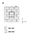
続いて、視差画素と視差なし画素が混在する撮像素子の画素配列について図12〜図14を用いて説明する。図12〜図14では、視差なし画素の開口部の開口形状を調整する場合について示している。なお、マイクロレンズを変形する場合には、視差なし画素の開口マスクとして全開口の開口マスクを用いればよい。図12は、本実施形態の画素配列の一例を示す図である。図12に示す撮像素子100は、図の太線で示す2×2画素のパターン110を基本格子とする。パターン110において、左上の画素および右下の画素に視差なし画素が割り当てられている。また、左下の画素に視差Lt画素が割り当てられ、右上の画素に視差Rt画素が割り当てられている。ここでは、撮像素子100は、モノクロセンサである。図12に示す撮像素子100の配列は、N:Lt:Rt=2:1:1である。
Next, a pixel arrangement of an image sensor in which parallax pixels and non-parallax pixels are mixed will be described with reference to FIGS. 12 to 14 show a case where the opening shape of the opening of the pixel without parallax is adjusted. Note that, when the microlens is deformed, an opening mask with all openings may be used as an opening mask for pixels without parallax. FIG. 12 is a diagram illustrating an example of a pixel array of the present embodiment. The
図13は、本実施形態の画素配列のバリエーションを示す図である。図13に示す撮像素子100は、隣接する8画素×8画素のパターン110を基本格子とする。パターン110は、2×2の4画素を基本単位とするベイヤー配列を、Y軸方向に4つ、X軸方向に4つ含む。なお、図示するように、ベイヤー配列においては、左上画素と右下画素に緑フィルタ(Gフィルタ)、左下画素に青フィルタ(Bフィルタ)、右上画素に赤フィルタ(Rフィルタ)が配される。
FIG. 13 is a diagram illustrating a variation of the pixel arrangement of the present embodiment. The
パターン110内の画素をPIJで表す。例えば、左上画素はP11であり、右上画素はP81である。図に示すように、視差画素は以下のように配列されている。
Pixels in the
P11…視差Lt画素+Gフィルタ(=G(Lt))
P51…視差Rt画素+Gフィルタ(=G(Rt))
P32…視差Lt画素+Bフィルタ(=B(Lt))
P72…視差Rt画素+Bフィルタ(=B(Rt))
P23…視差Rt画素+Rフィルタ(=R(Rt))
P63…視差Lt画素+Rフィルタ(=R(Lt))
P44…視差Rt画素+Gフィルタ(=G(Rt))
P84…視差Lt画素+Gフィルタ(=G(Lt))
P15…視差Rt画素+Gフィルタ(=G(Rt))
P55…視差Lt画素+Gフィルタ(=G(Lt))
P36…視差Rt画素+Bフィルタ(=B(Rt))
P76…視差Lt画素+Bフィルタ(=B(Lt))
P27…視差Lt画素+Rフィルタ(=R(Lt))
P67…視差Rt画素+Rフィルタ(=R(Rt))
P48…視差Lt画素+Gフィルタ(=G(Lt))
P88…視差Rt画素+Gフィルタ(=G(Rt))
他の画素は視差なし画素であり、視差無し画素+Rフィルタ、視差なし画素+Gフィルタ、視差無し画素+Bフィルタのいずれかである。ここでは、撮像素子100は、カラーセンサである。図13に示す撮像素子100の配列は、N:Lt:Rt=6:1:1である。
P 11 : Parallax Lt pixel + G filter (= G (Lt))
P 51 ... Parallax Rt pixel + G filter (= G (Rt))
P 32 ... Parallax Lt pixel + B filter (= B (Lt))
P 72 ... Parallax Rt pixel + B filter (= B (Rt))
P 23 ... Parallax Rt pixel + R filter (= R (Rt))
P 63 ... Parallax Lt pixel + R filter (= R (Lt))
P 44 ... Parallax Rt pixel + G filter (= G (Rt))
P 84 ... parallax Lt pixel + G filter (= G (Lt))
P 15 ... Parallax Rt pixel + G filter (= G (Rt))
P 55 ... Parallax Lt pixel + G filter (= G (Lt))
P 36 ... Parallax Rt pixel + B filter (= B (Rt))
P 76 ... Parallax Lt pixel + B filter (= B (Lt))
P 27 ... Parallax Lt pixel + R filter (= R (Lt))
P 67 ... Parallax Rt pixel + R filter (= R (Rt))
P 48 ... Parallax Lt pixel + G filter (= G (Lt))
P 88 ... Parallax Rt pixel + G filter (= G (Rt))
The other pixels are non-parallax pixels, and are any of the non-parallax pixel + R filter, the non-parallax pixel + G filter, and the non-parallax pixel + B filter. Here, the
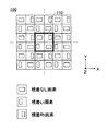
図14は、本実施形態の画素配列のバリエーションを示す図である。図14に示す撮像素子100は、隣接する8画素×8画素のパターン110を基本格子とする。パターン110は、2×2の4画素を基本単位とするベイヤー配列を、Y軸方向に4つ、X軸方向に4つ含む。また、図に示すように、視差画素は以下のように配列されている。
FIG. 14 is a diagram showing variations of the pixel arrangement of the present embodiment. The
P11…視差Lt画素+Gフィルタ(=G(Lt))
P51…視差Rt画素+Gフィルタ(=G(Rt))
P32…視差Lt画素+Bフィルタ(=B(Lt))
P63…視差Rt画素+Rフィルタ(=R(Rt))
P15…視差Rt画素+Gフィルタ(=G(Rt))
P55…視差Lt画素+Gフィルタ(=G(Lt))
P76…視差Rt画素+Bフィルタ(=B(Rt))
P27…視差Lt画素+Rフィルタ(=R(Lt))
他の画素は視差なし画素であり、視差無し画素+Rフィルタ、視差なし画素+Gフィルタ、視差無し画素+Bフィルタのいずれかである。ここでは、撮像素子100は、カラーセンサである。図14に示す撮像素子100の配列は、N:Lt:Rt=14:1:1である。
P 11 : Parallax Lt pixel + G filter (= G (Lt))
P 51 ... Parallax Rt pixel + G filter (= G (Rt))
P 32 ... Parallax Lt pixel + B filter (= B (Lt))
P 63 ... Parallax Rt pixel + R filter (= R (Rt))
P 15 ... Parallax Rt pixel + G filter (= G (Rt))
P 55 ... Parallax Lt pixel + G filter (= G (Lt))
P 76 ... Parallax Rt pixel + B filter (= B (Rt))
P 27 ... Parallax Lt pixel + R filter (= R (Lt))
The other pixels are non-parallax pixels, and are any of the non-parallax pixel + R filter, the non-parallax pixel + G filter, and the non-parallax pixel + B filter. Here, the
図13においては、撮像素子100の全体でみた場合に、視差画素は、Gフィルタを有する第1群と、Rフィルタを有する第2群と、Bフィルタを有する第3群のいずれかに区分され、パターン110には、それぞれの群に属する視差Lt画素および視差Rt画素が少なくとも1つは含まれる。図の例のように、これらの視差画素および視差なし画素のそれぞれが、パターン110内においてできるだけ等方性を有して配置されるとよい。なお、視差画素および視差なし画素が混合して配置されているので、一見ランダムに配置されるように見える。等方性を有して配置されることにより、色成分ごとの空間分解能に偏りを生じさせることなく、視差画素の出力としてRGBのカラー情報を取得することができるので、高品質な視差画像データが得られる。
In FIG. 13, the parallax pixels are divided into one of a first group having a G filter, a second group having an R filter, and a third group having a B filter when viewed from the
以上のそれぞれの配列において、視差なし画素の開口部の開口形状は、如何なる長方形状(矩形形状)をとればよいか説明する。それぞれの配列において視差画素の密度が異なるので、非対称ボケの影響度合いも異なると推察される。非対称ボケの影響度合いは、後の各実施形態で説明する画像処理を通して、中間的に生成される2D画像におけるボケで測定するものとする。なぜならば、後述する視差変調という画像処理を通して最終的に生成される3D画像は、右目用画像と左目用画像を単純に重ね合わせて表示すると中間的に生成された2D画像と同じ状態に見えるからである。 In each of the above arrangements, a description will be given of what rectangular shape (rectangular shape) the opening shape of the opening portion of the non-parallax pixel should be. Since the density of parallax pixels is different in each array, it is assumed that the degree of influence of asymmetric blur is also different. It is assumed that the degree of influence of asymmetric blur is measured by blur in a 2D image generated intermediately through image processing described in each embodiment below. This is because a 3D image that is finally generated through image processing called parallax modulation, which will be described later, appears to be the same state as an intermediately generated 2D image when a right-eye image and a left-eye image are simply superimposed and displayed. It is.
全画素数に占める視差画素の総数の割合(視差画素の密度)がδで表される場合に、視差なし画素の開口部における垂直方向の変形割合vをδの関数として表す。ただし、視差画素の密度は、互いに同数の左視差画素と右視差画素の和であり、視差なし画素と左視差画素と右視差画素の密度比が下記の(式1)で表されるとする。 When the ratio of the total number of parallax pixels in the total number of pixels (density of parallax pixels) is represented by δ, the deformation ratio v in the vertical direction at the opening of the pixel without parallax is represented as a function of δ. However, the density of the parallax pixels is the sum of the same number of the left parallax pixels and the right parallax pixels, and the density ratio of the non-parallax pixels, the left parallax pixels, and the right parallax pixels is expressed by the following (Formula 1). .
N:Lt:Rt=1−δ : δ/2 : δ/2 (式1)
上述した中間的に生成される2D画像を生成するにあたって、以下の実施形態で述べる画像処理では、視差なし画素の画素値と視差画素の画素値を密度比に応じて混合する処理を行う。これにより、全ての画素でサンプリングした空間情報を最大限に生かすことができる。実際には、画像処理部205は、撮像素子100の画素配列順にその出力値(画素値)が羅列されたRAW元画像データを受け取り、複数のプレーンデータに分離するプレーン分離処理を実行する。プレーンデータとは、同一に特徴付けられた画素グループごとに分離して寄せ集められた画像データである。画像処理部205は、まず視差画素の画素値を除去して、空格子とする。そして、空格子となった画素値を、周辺の視差なし画素の画素値を用いて補間処理により算出する。これにより、空格子が埋められたN画像を生成する。
N: Lt: Rt = 1−δ: δ / 2: δ / 2 (Formula 1)
In generating the above-described intermediately generated 2D image, in the image processing described in the following embodiment, a process of mixing the pixel value of the non-parallax pixel and the pixel value of the parallax pixel according to the density ratio is performed. Thereby, the spatial information sampled by all the pixels can be utilized to the maximum extent. In practice, the
同様に、画像処理部205は、撮像素子100の全出力値から左視差画素の画素値以外の画素値を除去して空格子とする。そして、空格子となった画素値を、周辺の左視差画素の画素値を用いて補間処理により算出する。これにより、空格子が埋められたLt画像を生成する。さらに画像処理部205は、撮像素子100の全出力値から右視差画素の画素値以外の画素値を除去して空格子とする。そして、空格子となった画素値を、周辺の右視差画素の画素値を用いて補間処理により算出する。これにより、空格子が埋められたRt画像を生成する。その後、Lt画像とRt画像の平均画像を生成すると、当該平均画像も別な空間情報を備えた視差なし画像を表している。したがって、N画像と、Lt画像とRt画像の平均画像の2種類の視差なし画像を混合して、新たに1つに統合した視差なし画像N'を生成する。これを各画素位置上で行う。ここでは、視差画素密度に応じた相乗平均をとる例を示す。これは後述するローカル・ゲインバランス補正と呼ばれる処理ステップで行う。
Similarly, the
これを模式的に表すと密度比δの関数で表すことができる(式2)。
中間2D画像を視差画素の密度の関数として生成するので、δの極限値、すなわち、δ→1の場合には視差画素のみで作成した画像となり、δ→0の場合には視差なし画素のみで作成した画像となる。この極限状態で、視差なし画素の開口部の開口形状a:bが如何なる値を採るべきかを考察すると、δの関数として表す場合の出発点の境界条件が与えられる。
This can be schematically expressed as a function of the density ratio δ (Formula 2).
Since an intermediate 2D image is generated as a function of the density of parallax pixels, the limit value of δ, that is, an image created only with parallax pixels when δ → 1, and only with no parallax pixels when δ → 0. It will be the created image. Considering what value the aperture shape a: b of the aperture of the non-parallax pixel should take in this limit state, the boundary condition of the starting point when expressed as a function of δ is given.
δ→1の場合には視差画素のみで構成されるので、視差なし画素が存在しない。したがって、視差なし画素による補正はできない。δ→0の場合には視差なし画素のみで構成されるので、通常の2D専用センサと同等になり、視差なし画素の開口形状を変形する必要はない。したがって、v=0である。これは他が如何なる条件になろうとも常に成り立っていなければならない。したがって、v=0∝δと置くことができる。つまり、δが0の近傍において、vはδに比例する。δ=0の場合にはv=0となる。 In the case of δ → 1, since it is composed only of parallax pixels, there is no non-parallax pixel. Accordingly, correction using non-parallax pixels is not possible. In the case of δ → 0, it is composed only of pixels without parallax, so it is equivalent to a normal 2D dedicated sensor, and there is no need to change the aperture shape of pixels without parallax. Therefore, v = 0. This must always be true no matter what the other conditions are. Therefore, v = 0 置 く δ can be set. That is, when δ is near 0, v is proportional to δ. When δ = 0, v = 0.
次に、視差画素が半開口の状態から、水平方向に開口を広げた場合に、視差画素の開口形状の関数として視差なし画素の開口形状の変形割合vを表す場合について説明する。図15は、視差画素の開口マスクの開口形状を説明する図である。視差Lt画素の開口部104lは、中心線322から右側に幅uだけ延伸している。一方、視差Rt画素の開口部104rは、中心線322から左側に幅uだけ延伸している。視差画素の開口部は、(式3)で表すことができる。
Next, a case where the deformation ratio v of the aperture shape of the non-parallax pixel is expressed as a function of the aperture shape of the parallax pixel when the aperture is expanded in the horizontal direction from the state where the parallax pixel is a half aperture will be described. FIG. 15 is a diagram illustrating the opening shape of the opening mask of the parallax pixels. The opening 104l of the parallax Lt pixel extends from the
水平開口幅:垂直開口幅=((1/2)+u):1 (式3)
この場合においても、まず初めに極限状態が如何なる境界条件を与えるかを考察する。視差画素の開口が全開口にまで広がる極限u→1/2を想定する。この場合には、視差画素は視差なし画素として扱うことができるので、全てが視差なし画素となる。したがって、視差画素の密度に関係なく任意のδに対して、常に視差なし画素を変形する必要はない。つまり、v=0となる。これは他が如何なる条件を採ろうとも常に成り立っていなければならないので、v=0∝((1/2)−u)と置くことができる。
Horizontal opening width: Vertical opening width = ((1/2) + u): 1 (Formula 3)
Even in this case, first, the boundary condition given by the extreme state is considered. Assume the limit u → 1/2 where the opening of the parallax pixel extends to the entire opening. In this case, since the parallax pixels can be handled as non-parallax pixels, all of them are non-parallax pixels. Therefore, it is not always necessary to transform a non-parallax pixel for an arbitrary δ regardless of the density of the parallax pixel. That is, v = 0. Since this must always hold regardless of other conditions, v = 0 置 く ((1/2) −u) can be set.
以上をまとめると、(式4)、(式5)、(式6)となる。
δ=1の場合 補正不能 (式4)
δ=0の場合 常にv=0∝δ (式5)
任意のδに対して、u=1/2の場合 常にv=0∝((1/2)−u) (式6)
以上から、(式7)を導くことができる。
v∝δ((1/2)−u) (式7)
In summary, (Expression 4), (Expression 5), and (Expression 6) are obtained.
When δ = 1 Correction not possible (Formula 4)
When δ = 0, always v = 0∝δ (Formula 5)
For any δ, when u = 1/2, v = 0 = ((1/2) −u) (Equation 6)
From the above, (Equation 7) can be derived.
v ∝δ ((1/2) −u) (Formula 7)
vがδと((1/2)−u)と比例関係にあることがわかったので、次にその比例係数を決めて絶対量を表現する。絶対量を表現するにあたって、視差画素が半開口の状態u=0で構成される単純な場合を考察するのがよい。更に、視差画素の密度がδ=1/2である図12に示されるN:Lt:Rt=2:1:1の配列を考える。図12の一方のN画素がLt画素の非対称ボケを補正し、他方のN画素がRt画素の非対称ボケを補正する役割を担うと仮定すると、N:Lt:Rt=1−δ : δ/2 : δ/2であるので一般的に(式8)に示す関係が導かれる。
v=δ/2 (式8)
図12〜図14で示す画素配列の場合に、視差なし画素の変形割合vは如何なる値を採るかを以下に示す。
Since it was found that v is proportional to δ and ((1/2) -u), the proportionality coefficient is then determined to express the absolute quantity. In expressing the absolute quantity, it is better to consider the simple case where the parallax pixel is configured with a half-open state u = 0. Further, consider an array of N: Lt: Rt = 2: 1: 1 shown in FIG. 12 where the density of parallax pixels is δ = 1/2. Assuming that one N pixel in FIG. 12 corrects the asymmetric blur of the Lt pixel and the other N pixel plays a role of correcting the asymmetric blur of the Rt pixel, N: Lt: Rt = 1−δ: δ / 2 : Since δ / 2, the relationship shown in (Expression 8) is generally derived.
v = δ / 2 (Formula 8)
In the case of the pixel arrangement shown in FIGS. 12 to 14, it is shown below what value the deformation ratio v of the non-parallax pixel takes.
図12に示したように、N:Lt:Rt=2:1:1、すなわちδ=1/2の場合には、(式9)となる。
V=1/4 (式9)
図13に示したように、N:Lt:Rt=6:1:1、すなわちδ=1/4の場合には、(式10)となる。
V=1/8 (式10)
図14に示したように、N:Lt:Rt=14:1:1、すなわちδ=1/8の場合には、(式11)となる。
V=1/16 (式11)
As shown in FIG. 12, when N: Lt: Rt = 2: 1: 1, that is, δ = 1/2, (Equation 9) is obtained.
V = 1/4 (Formula 9)
As shown in FIG. 13, when N: Lt: Rt = 6: 1: 1, that is, δ = 1/4, (Equation 10) is obtained.
V = 1/8 (Formula 10)
As shown in FIG. 14, when N: Lt: Rt = 14: 1: 1, that is, δ = 1/8, (Equation 11) is obtained.
V = 1/16 (Formula 11)
上記(式7)においてu=0の場合に(式8)が成り立つので、比例定数は1であることがわかる。一般式として(式12)を導出できる。
v=δ×((1/2)−u) (式12)
したがって、視差なし画素の開口マスクにおける矩形形状の長辺と短辺の比a:b、あるいはマイクロレンズの楕円形状の長軸径と短軸径の比a:bは次のように表すことができる。
a:b=1:1−δ×((1/2)−u) (式13)
(式13)は、uが負の領域についても成り立つ。つまり、|u|<1/2である。また、0<δ<1である。
Since (Expression 8) is established when u = 0 in the above (Expression 7), it can be seen that the proportionality constant is 1. (Formula 12) can be derived as a general formula.
v = δ × ((1/2) −u) (Formula 12)
Therefore, the ratio a: b of the long side and the short side of the rectangular shape in the aperture mask of the pixel without parallax, or the ratio a: b of the major axis diameter to the minor axis diameter of the elliptical shape of the microlens can be expressed as follows. it can.
a: b = 1: 1−δ × ((1/2) −u) (Formula 13)
(Equation 13) also holds for a region where u is negative. That is, | u | <1/2. Also, 0 <δ <1.
u=0の場合において、図12〜図14で示す画素配列の場合のaとbの比を示す。
図12に示したように、N:Lt:Rt=2:1:1、すなわちδ=1/2の場合には、(式14)となる。
a:b=1:1−1/4=4:3 (式14)
図13に示したように、N:Lt:Rt=6:1:1、すなわちδ=1/4の場合には、(式15)となる。
a:b=1:1−1/8=8:7 (式15)
図14に示したように、N:Lt:Rt=14:1:1、すなわちδ=1/8の場合には、(式16)となる。
a:b=1:1−1/16=16:15 (式16)
In the case of u = 0, the ratio of a and b in the pixel array shown in FIGS.
As shown in FIG. 12, when N: Lt: Rt = 2: 1: 1, that is, δ = 1/2, (Equation 14) is obtained.
a: b = 1: 1-1 / 4 = 4: 3 (Formula 14)
As shown in FIG. 13, when N: Lt: Rt = 6: 1: 1, that is, δ = 1/4, (Equation 15) is obtained.
a: b = 1: 1-1 / 8 = 8: 7 (Formula 15)
As shown in FIG. 14, when N: Lt: Rt = 14: 1: 1, that is, δ = 1/8, (Equation 16) is obtained.
a: b = 1: 1-1 / 16 = 16: 15 (Formula 16)
<実施形態1>
ここでは、撮像素子100の配列として図12で示した配列を採用する。すなわち、撮像素子100はモノクロセンサであり、撮像素子100の配列は、N:Lt:Rt=2:1:1である。視差なし画素の構成は、次のどちらか1つを採る。すなわち、開口部の長辺と短辺の比がa:b=4:3である開口マスクを用いるか、長軸径と短軸径の比がa:b=4:3となる楕円形状に集光特性を変形したマイクロレンズを用いるか、のいずれかである。以下にそうして撮像された画像データを現像する画像処理を示す。画像処理の手順は、およそ以下の通りである。
<
Here, the arrangement shown in FIG. 12 is adopted as the arrangement of the
1)視差多重化モザイク画像データ入力
2)視差モザイク画像のグローバル・ゲインバランス補正
3)仮の視差画像の生成
4)左右の局所照度分布補正による視差なし基準画像の生成
(ローカル・ゲインバランス補正)
5)実際の視差画像の生成
6)出力空間への変換
以下、順に説明する。
1) Input of parallax multiplexed mosaic image data 2) Global gain balance correction of parallax mosaic image 3) Generation of temporary parallax image 4) Generation of parallax-free reference image by left and right local illuminance distribution correction (local gain balance correction)
5) Generation of actual parallax image 6) Conversion to output space Hereinafter, description will be made in order.
1)視差多重化モザイク画像データ入力
図12の視差が多重化された単板式モノクロのモザイク画像をM(x,y)で表す。階調はA/D変換によって出力された線形階調であるものとする。
1) Input of parallax multiplexed mosaic image data A single-panel monochrome mosaic image in which the parallax of FIG. 12 is multiplexed is represented by M (x, y). It is assumed that the gradation is a linear gradation output by A / D conversion.
便宜的にモザイク画像M(x,y)の内、視差なし画素の信号面をNmosaic(x,y)、左視差画素の信号面をLtmosaic(x,y)、右視差画素の信号面をRtmosaic(x,y)、と表すことにする。 For convenience, in the mosaic image M (x, y), the non-parallax pixel signal surface is N mosaic (x, y), the left parallax pixel signal surface is L mosaic (x, y), and the right parallax pixel signal surface. Is expressed as Rt mosaic (x, y).
こうして視差なし画素が1つのゲイン係数で、左視差画素が1つのゲイン係数で、右視差画素が1つのゲイン係数で補正されたモザイク画像をM'(x,y)として出力する。 Thus, a mosaic image in which the non-parallax pixel is corrected with one gain coefficient, the left parallax pixel with one gain coefficient, and the right parallax pixel with one gain coefficient is output as M ′ (x, y).
3)仮の視差画像の生成
空間周波数解像度の低い分解能である仮の左視差画像と、空間周波数解像度の低い分解能である仮の右視差画像を生成する。左視差画素ばかりを集めた信号面内の単純平均補間を行う。近接して存在する画素値を用いて、距離の比に応じて線形補間を行う。同様に、右視差画素ばかりを集めた信号面内の単純平均補間を行う。同様に、視差なし画素ばかりを集めた信号面内の単純平均補間を行う。すなわち、Ltmosaic(x,y)からLt(x,y)を、Rtmosaic(x,y)からRt(x,y)を、Nmosaic(x,y)からN(x,y)を生成する。仮の視差なし画像をN(x,y)、仮の左視差画像をLt(x,y)、仮の右視差画像をRt(x,y)と表す。なお、仮の視差なし画像N(x,y)を生成する場合には、信号面内での方向判定を導入して高精細に行うのがよい。
3) Generation of temporary parallax image A temporary left parallax image having a low spatial frequency resolution and a temporary right parallax image having a low spatial frequency resolution are generated. Simple average interpolation is performed in the signal plane that collects only the left parallax pixels. Linear interpolation is performed according to the distance ratio using pixel values that are close to each other. Similarly, simple average interpolation is performed in the signal plane in which only the right parallax pixels are collected. Similarly, simple average interpolation is performed in the signal plane in which only non-parallax pixels are collected. That is, generation Lt mosaic (x, y) from Lt (x, y) and, Rt mosaic (x, y) from the Rt (x, y) and, N mosaic (x, y) from the N (x, y) and To do. A temporary non-parallax image is represented as N (x, y), a temporary left parallax image is represented as Lt (x, y), and a temporary right parallax image is represented as Rt (x, y). When generating a temporary non-parallax image N (x, y), it is preferable to introduce a direction determination in the signal plane and perform it with high definition.
4)左右の照度分布補正による視差なし基準画像の生成
(ローカル・ゲインバランス補正)
次にステップ1で行ったグローバル・ゲイン補正と同様の考え方で、画素単位のローカル・ゲイン補正を行うことによって、まず画面内の左視差画素と画面内の右視差画素の照度を合わせる。この操作によって左右間の視差を消滅させる。その上で左右平均をとった信号面と視差なし画素の撮像信号面との間でさらに照度を合わせる。そうして、全ての画素でゲイン整合のとれた新しい視差なしの基準画像面を作成する。これは平均値と置き換えることと等価であり、視差の消滅した中間画像面が出来上がる。これをN(x,y)と書くことにする。
4) Generation of parallax-free reference images by correcting left and right illuminance distribution (local gain balance correction)
Next, by performing local gain correction in units of pixels in the same manner as the global gain correction performed in
5)実際の視差画像の生成
ステップ3で生成した解像力の低い仮の左視差画像Lt(x,y)とステップ5で中間処理として生成した解像力の高い視差なしのモノクロ画像N(x,y)を用いて、実際に出力する解像力の高い左視差のモノクロ画像Lt'(x,y)を生成する。同様に、ステップ3で生成した解像力の低い仮の右視差画像Rt(x,y)とステップ5で中間処理として生成した解像力の高い視差なしのモノクロ画像N(x,y)を用いて、実際に出力する解像力の高い右視差のカラー画像Rt'(x,y)を生成する。
5) Generation of actual parallax image Temporary left parallax image Lt (x, y) generated in step 3 and low-resolution monochrome image N (x, y) generated as intermediate processing in step 5 Is used to generate a left-parallax monochrome image Lt ′ (x, y) with high resolving power that is actually output. Similarly, using the temporary right parallax image Rt (x, y) generated in step 3 with low resolution and the monochrome image N (x, y) without parallax generated as intermediate processing in step 5 with actual resolution, A right parallax color image Rt ′ (x, y) with high resolving power is generated.
視差なしのモノクロ画像は、全開口のボケ幅と一致する被写体像を形成している。したがって、比を一定に保つ視差変調の分母には、左視点像と右視点像の相加平均による全開口のボケ幅を持った像を基準点にとり、視差変調後の左右の画像が再度、半開口のボケ幅をもつ像となるように変調を加える。 A monochrome image without parallax forms a subject image that matches the blur width of the entire aperture. Therefore, in the denominator of the parallax modulation that keeps the ratio constant, an image with the blur width of the full aperture by the arithmetic mean of the left viewpoint image and the right viewpoint image is taken as a reference point, and the left and right images after the parallax modulation are again Modulation is applied so that the image has a half-aperture blur width.
6)出力色空間への変換
こうして得られた高解像な視差なしの中間モノクロ画像N(x,y)と高解像の左視差のモノクロ画像Lt'(x,y)、高解像の右視差のモノクロ画像Rt'(x,y)のそれぞれを適当なガンマ変換を行って出力空間の画像として出力する。
6) Conversion to output color space The high-resolution non-parallax intermediate monochrome image N (x, y) and the high-resolution left-parallax monochrome image Lt ′ (x, y) obtained in this way Each right-parallax monochrome image Rt ′ (x, y) is subjected to appropriate gamma conversion and output as an output space image.
<実施形態2>
ここでは、撮像素子100の配列として図14で示した配列を採用する。すなわち、撮像素子100はカラーセンサであり、撮像素子100の配列は、N:Lt:Rt=14:1:1である。視差なし画素の構成は、次のどちらか1つを採る。すなわち、開口部の長辺と短辺の比がa:b=16:15となる開口マスクを用いるか、長軸と短軸の比がa:b=16:15となる楕円形状に集光特性を変形したマイクロレンズを用いるか、のいずれかである。以下にそうして撮像された画像データを現像する画像処理を示す。画像処理の手順は、およそ以下の通りである。
<
Here, the arrangement shown in FIG. 14 is adopted as the arrangement of the
1)色・視差多重化モザイク画像データ入力
2)色・視差モザイク画像のグローバル・ゲインバランス補正
3)仮の視差画像の生成
4)左右の局所照度分布補正による視差なし色モザイク画像の生成
(ローカル・ゲインバランス補正)
5)視差なし基準画像の生成
6)実際の視差画像の生成
7)出力色空間への変換
以下、順に説明する。
1) Color / parallax multiplexed mosaic image data input 2) Global gain balance correction of color / parallax mosaic image 3) Temporary parallax image generation 4) Generation of parallax-free color mosaic image by right and left local illuminance distribution correction (Local・ Gain balance correction
5) Generation of reference image without parallax 6) Generation of actual parallax image 7) Conversion to output color space
1)色・視差多重化モザイク画像データ入力
図14の色と視差の多重化された単板式モザイク画像をM(x,y)で表す。階調はA/D変換によって出力された線形階調であるものとする。
1) Color / Parallax Multiplexed Mosaic Image Data Input A single-panel mosaic image in which the color and parallax in FIG. 14 are multiplexed is represented by M (x, y). It is assumed that the gradation is a linear gradation output by A / D conversion.
便宜的にモザイク画像M(x,y)の内、R成分の視差なし画素の信号面をRN_mosaic(x,y)、R成分の左視差画素の信号面をRLt_mosaic(x,y)、R成分の右視差画素の信号面をRRt_mosaic(x,y)、G成分の左視差画素の信号面をGN_mosaic(x,y)、G成分の視差なし画素の信号面をGLt_mosaic(x,y)、G成分の右視差画素の信号面をGRt_mosaic(x,y)、B成分の視差なし画素の信号面をBN_mosaic(x,y)、B成分の左視差画素の信号面をBLt_mosaic(x,y)、B成分の右視差画素の信号面をBRt_mosaic(x,y)と表すことにする。 Convenience of the mosaic image M (x, y), a signal surface of parallax without the R component pixel R N_mosaic (x, y), a signal surface of the left parallax pixels of the R component R Lt_mosaic (x, y), the signal surface of the right parallax pixels of the R component R Rt_mosaic (x, y), a signal surface of the left parallax pixels of the G component G N_mosaic (x, y), a signal surface of parallax without the G component pixel G Lt_mosaic (x , Y), the signal surface of the right parallax pixel of G component is GRt_mosaic (x, y), the signal surface of the non- parallax pixel of B component is BN_mosaic (x, y), and the signal surface of the left parallax pixel of B component is Let B Lt_mosaic (x, y) and the signal surface of the B component right parallax pixel be B Rt_mosaic (x, y).
こうして視差なし画素が1つのゲイン係数で、左視差画素が1つのゲイン係数で、右視差画素が1つのゲイン係数で補正されたモザイク画像をM'(x,y)として出力する。 Thus, a mosaic image in which the non-parallax pixel is corrected with one gain coefficient, the left parallax pixel with one gain coefficient, and the right parallax pixel with one gain coefficient is output as M ′ (x, y).
3)仮の視差画像の生成
空間周波数解像度の低い分解能である仮の左視差画像と、空間周波数解像度の低い分解能である仮の右視差画像を生成する。左視差画素ばかりを集めたG色面内の単純平均補間を行う。近接して存在する画素値を用いて、距離の比に応じて線形補間を行う。同様に、右視差画素ばかりを集めたG色面内の単純平均補間を行う。同様に、視差なし画素ばかりを集めたG色面内の単純平均補間を行う。同様の処理をR,G,Bの各々について行う。すなわち、RLt_mosaic(x,y)からRLt(x,y)を、RRt_mosaic(x,y)からRRt(x,y)を、RN_mosaic(x,y)からRN(x,y)を、GLt_mosaic(x,y)からGLt(x,y)を、GRt_mosaic(x,y)からGRt(x,y)を、GN_mosaic(x,y)からGN(x,y)を、BLt_mosaic(x,y)からBLt(x,y)を、BRt_mosaic(x,y)からBRt(x,y)を、BN_mosaic(x,y)からBN(x,y)を生成する。
3) Generation of temporary parallax image A temporary left parallax image having a low spatial frequency resolution and a temporary right parallax image having a low spatial frequency resolution are generated. Simple average interpolation is performed in the G color plane where only the left parallax pixels are collected. Linear interpolation is performed according to the distance ratio using pixel values that are close to each other. Similarly, simple average interpolation in the G color plane in which only the right parallax pixels are collected is performed. Similarly, simple average interpolation in the G color plane in which only non-parallax pixels are collected is performed. Similar processing is performed for each of R, G, and B. That is, R Lt_mosaic (x, y) to R Lt (x, y), R Rt_mosaic (x, y) to R Rt (x, y), and R N_mosaic (x, y) to R N (x, y) ) and, G Lt_mosaic (x, y) from the G Lt (x, a y), G Rt_mosaic (x, G Rt the (x, y) from y), G N_mosaic (x, y) from G N (x, y), B Lt_mosaic (x, y) to B Lt (x, y), B Rt_mosaic (x, y) to B Rt (x, y), B N_mosaic (x, y) to B N (x, y) , Y).
ここで、仮のR成分の視差なし画像をRN(x,y)、仮のG成分の視差なし画像をGN(x,y)、仮のB成分の視差なし画像をBN(x,y)、仮のR成分の左視差画像をRLt(x,y)、仮のG成分の左視差画像をGLt(x,y)、仮のB成分の左視差画像をBLt(x,y)で表す。同様に、仮のR成分の右視差画像をRRt(x,y)、仮のG成分の右視差画像をGRt(x,y)、仮のB成分の右視差画像をBRt(x,y)で表す。なお、仮の視差なし画像RN(x,y)、GN(x,y)、BN(x,y)を生成する場合には、信号面内での方向判定を導入して高精細に行うのがよい。 Here, the temporary R component non-parallax image is R N (x, y), the temporary G component non-parallax image is G N (x, y), and the temporary B component non-parallax image is B N (x , Y), the left parallax image of the temporary R component is R Lt (x, y), the left parallax image of the temporary G component is G Lt (x, y), and the left parallax image of the temporary B component is B Lt ( x, y). Similarly, the right parallax image of the temporary R component is R Rt (x, y), the right parallax image of the temporary G component is G Rt (x, y), and the right parallax image of the temporary B component is B Rt (x , Y). In the case of generating temporary non-parallax images R N (x, y), G N (x, y), and B N (x, y), high-definition is introduced by introducing direction determination in the signal plane. Good to do.
4)左右の照度分布補正による視差なし色モザイク画像の生成
(ローカル・ゲインバランス補正)
次にステップ1で行ったグローバル・ゲイン補正と同様の考え方で、画素単位のローカル・ゲイン補正を行うことによって、まず画面内の左視差画素と画面内の右視差画素の照度を合わせる。この操作によって左右間の視差を消滅させる。その上で左右平均をとった信号面と視差なし画素の撮像信号面との間でさらに照度を合わせる。以上により、全ての画素でゲイン整合のとれた新しいBayer面を作成する。これは平均値と置き換えることと等価であり、視差の消滅したBayer面が出来上がる。これをMN(x,y)と書くことにする。
4) Generation of parallax-free color mosaic image by correcting left and right illumination distribution (local gain balance correction)
Next, by performing local gain correction in units of pixels in the same manner as the global gain correction performed in
なお、視差なし画素の開口マスクは全開口である。したがって、左右間で視差消滅させた被写体像のボケ幅を全開口のボケ幅と一致させる目的で相加平均を用いる。これにより、左右間の視差を消滅させる。 Note that the aperture mask of the non-parallax pixel is a full aperture. Therefore, an arithmetic average is used in order to make the blur width of the subject image whose parallax disappeared between the left and right coincide with the blur width of the entire aperture. This eliminates the parallax between the left and right.
さらに、左右間で視差消滅させた信号面と視差なし画素の撮像信号面との間で平均をとる操作は、両者が既に同じボケ幅の被写体像に揃えられているので、そのボケ幅を保存する必要がある。したがって、この場合には共通に相乗平均をとらなければならない。ここで、視差画素の数は視差なし画素の数より少ない。加えて、視差画像の解像力は、視差なし画像の解像力より低い。したがって、視差なし画素の画素値と左右の視差画素の平均値とに対する重みの配分を均等にすると、得られる画像の解像力は、視差画像の解像力の影響により全体として低下する。よって、視差なし画像の解像力に可能な限り近づける工夫が必要になる。そこで、撮像素子上の画素配列における視差なし画素と視差画素の密度比を考慮に入れて相乗平均をとるとよい。具体的には、実施形態2で用いた視差なし画素(N)と左視差画素(Lt)と右視差画素(Rt)の比は、N:Lt:Rt=14:1:1、すなわち、N:(Lt+Rt)=7:1であるので、視差なし画素には7/8乗の重みを、視差画素には1/8乗の重みを与えて、密度の高い視差なし画素を重視した配分とする。以下にそれらの具体式を挙げる。 Furthermore, the operation to take the average between the signal plane where the parallax disappeared between the left and right and the imaging signal plane of the non-parallax pixel is already aligned with the subject image of the same blur width, so the blur width is saved. There is a need to. Therefore, in this case, a common geometric average must be taken. Here, the number of parallax pixels is smaller than the number of non-parallax pixels. In addition, the resolution of the parallax image is lower than the resolution of the image without parallax. Therefore, if the distribution of weights is evenly distributed between the pixel value of the non-parallax pixel and the average value of the left and right parallax pixels, the resolution of the obtained image decreases as a whole due to the influence of the resolution of the parallax image. Therefore, it is necessary to devise as close as possible to the resolution of an image without parallax. Therefore, it is preferable to take a geometric average in consideration of the density ratio between the non-parallax pixels and the parallax pixels in the pixel array on the image sensor. Specifically, the ratio of the non-parallax pixel (N), the left parallax pixel (Lt), and the right parallax pixel (Rt) used in the second embodiment is N: Lt: Rt = 14: 1: 1, that is, N : (Lt + Rt) = 7: 1, so that the 7 / 8th power is given to the non-parallax pixels and the 1 / 8th power is given to the parallax pixels, and the distribution is focused on the high density non-parallax pixels. To do. The specific formulas are given below.
5)視差なし基準画像の生成
公知のBayer補間技術を行う。例として、本出願人と同一発明者のUSP7957588(WO2006/006373)やUSP8259213に示される補間アルゴリズムがある。
5) Generation of reference image without parallax A known Bayer interpolation technique is performed. As an example, there are interpolation algorithms shown in USP7957588 (WO2006 / 006373) and USP8259213 which are the same inventors as the present applicant.
6)実際の視差画像の生成
ステップ3で生成した解像力の低い仮の左視差のカラー画像RLt(x,y)、GLt(x,y)、BLt(x,y)とステップ5で中間処理として生成した解像力の高い視差なしのカラー画像RN(x,y)、GN(x,y)、BN(x,y)を用いて、実際に出力する解像力の高い左視差のカラー画像R'Lt(x,y)、G'Lt(x,y)、B'Lt(x,y)を生成する。同様に、ステップ3で生成した解像力の低い仮の右視差のカラー画像RRt(x,y)、GRt(x,y)、BRt(x,y)とステップ5で中間処理として生成した解像力の高い視差なしのカラー画像RN(x,y)、GN(x,y)、BN(x,y)を用いて、実際に出力する解像力の高い右視差のカラー画像R'Rt(x,y)、G'Rt(x,y)、B'Rt(x,y)を生成する。
6) Real parallax image generation Temporary left parallax color images R Lt (x, y), G Lt (x, y), B Lt (x, y) generated in step 3 and in step 5 Using the color images R N (x, y), G N (x, y), and B N (x, y) with high resolving power generated as intermediate processing, the left parallax with high resolving power that is actually output is output. Color images R ′ Lt (x, y), G ′ Lt (x, y), and B ′ Lt (x, y) are generated. Similarly, the provisional right parallax color images R Rt (x, y), G Rt (x, y), B Rt (x, y) generated in step 3 and intermediate processing in step 5 are generated. Using the color images R N (x, y), G N (x, y), and B N (x, y) without parallax with high resolving power, the color image R ′ Rt with high resolving power actually output is output. (X, y), G ′ Rt (x, y), and B ′ Rt (x, y) are generated.
視差なし画素の開口マスクは全開口である。したがって、視差変調の方式として相加平均を基準点にとる方式を採用することにより、視差画像のボケ幅を伝達しつつ、N画像と(Lt画像+Rt画像)/2のボケ幅の違いを補正するような視差変調効果を得る。 The aperture mask of the non-parallax pixel is a full aperture. Therefore, by adopting a method in which an arithmetic mean is used as a reference point as a method of parallax modulation, the blur width of the N image and (Lt image + Rt image) / 2 is reduced while transmitting the blur width of the parallax image. A parallax modulation effect to be corrected is obtained.
ここで、例えば高解像な左視差画像R'Ltを生成するにあたって、視差変調を行う場合も、撮像素子の画素配列における各視差画素同士の間でのRGBの密度比を考慮に入れた相乗平均をとる。すなわち、左視差画素同士の間ではR:G:B=1:2:1であり、右視差画素同士の間でもR:G:B=1:2:1であるので、R成分による視差変調に1/4乗の重みを、G成分による視差変調に1/2乗の重みを、B成分による視差変調に1/4乗の重みを与えて、密度の高いG成分による視差変調を重視した配分をとる。具体的には、以下の式を用いて高解像な左視差画像R'Lt、G'Lt、B'Ltと高解像な右視差画像R'Rt、G'Rt、B'Rtを算出する。 Here, for example, when generating the high-resolution left parallax image R ′ Lt , even when parallax modulation is performed, the synergy considering the density ratio of RGB between the parallax pixels in the pixel array of the image sensor is taken into consideration. Take the average. That is, since R: G: B = 1: 2: 1 between the left parallax pixels and R: G: B = 1: 2: 1 between the right parallax pixels, the parallax modulation by the R component is performed. Giving a weight of ¼ power, a weight of ½ power to parallax modulation by G component, and a weight of ¼ power to parallax modulation by B component, giving importance to parallax modulation by high density G component Take distribution. Specifically, high-resolution left parallax images R ′ Lt , G ′ Lt , B ′ Lt and high-resolution right parallax images R ′ Rt , G ′ Rt , B ′ Rt are calculated using the following equations. To do.
7)出力色空間への変換
こうして得られた高解像な視差なしの中間カラー画像RN(x,y)、GN(x,y)、BN(x,y)と高解像の左視差のカラー画像RLt(x,y)、GLt(x,y)、BLt(x,y)、高解像の右視差のカラー画像RRt(x,y)、GRt(x,y)、BRt(x,y)のそれぞれをセンサの分光特性のカメラRGBから標準的なsRGB色空間へ色マトリックス変換とガンマ変換を行って出力色空間の画像として出力する。
7) Conversion to output color space The high-resolution intermediate color images R N (x, y), G N (x, y), and B N (x, y) obtained in this way and high resolution Left parallax color images R Lt (x, y), G Lt (x, y), B Lt (x, y), High resolution right parallax color images R Rt (x, y), G Rt (x , Y), B Rt (x, y) are subjected to color matrix conversion and gamma conversion from the camera RGB having the spectral characteristics of the sensor to the standard sRGB color space, and output as an image in the output color space.
なお、撮像素子100の配列として図13で示した配列、すなわちN:Lt:Rt=6:1:1の配列を採用する場合には、視差なし画素の構成は、次のどちらか1つを採る。すなわち、開口部の長辺と短辺の比がa:b=8:7となる開口マスクを用いるか、長軸と短軸の比がa:b=8:7となる楕円形状に集光特性を変形したマイクロレンズを用いるか、の何れかである。現像処理は実施形態2と同様の手続きを経るので説明は省略する。ただし、ローカル・ゲインバランス補正の場合のN画像とLt画像とRt画像の混合割合が、視差画素の密度の変化に伴って変える必要がある。
Note that when the array shown in FIG. 13 is used as the array of the
以上の実施形態では、左右に視差をつける例を示したが、撮像素子と光学系を同時に90度回転すれば、上下視差の撮像系の実施形態となる。45度回転すれば斜め視差の撮像系の実施形態となる。 In the above embodiment, an example in which parallax is applied to the left and right has been described. However, if the image sensor and the optical system are simultaneously rotated by 90 degrees, an embodiment of an imaging system with vertical parallax is obtained. If it rotates 45 degrees, it will become embodiment of the imaging system of diagonal parallax.
特許文献2に示されるような、画素が正方形ではないハニカム構造であっても、N画素とLt画素とRt画素が混在する配列では同様の考え方が成り立つ。すなわち、左右に視差がつくように視差画素が構成されている場合は、左右視差の実施形態と同様にN画素を水平方向と垂直方向との間で視差画素と逆方向に変形する。
Even in a honeycomb structure in which pixels are not square as shown in
以上、本発明を実施の形態を用いて説明したが、本発明の技術的範囲は上記実施の形態に記載の範囲には限定されない。上記実施の形態に、多様な変更または改良を加えることが可能であることが当業者に明らかである。その様な変更または改良を加えた形態も本発明の技術的範囲に含まれ得ることが、特許請求の範囲の記載から明らかである。 As mentioned above, although this invention was demonstrated using embodiment, the technical scope of this invention is not limited to the range as described in the said embodiment. It will be apparent to those skilled in the art that various modifications or improvements can be added to the above-described embodiment. It is apparent from the scope of the claims that the embodiments added with such changes or improvements can be included in the technical scope of the present invention.
10 デジタルカメラ、20 撮影レンズ、21 光軸、22 絞り、100 撮像素子、101 マイクロレンズ、102 カラーフィルタ、103 開口マスク、104 開口部、104l 開口部、104r 開口部、104n 開口部、105 配線層、106 配線、108 光電変換素子、109 基板、110 パターン、201 制御部、202 A/D変換回路、203 メモリ、204 駆動部、205 画像処理部、207 メモリカードIF、208 操作部、209 表示部、210 LCD駆動回路、220 メモリカード、300 撮像素子、310 パターン、322 中心線、1801 分布曲線、1802 分布曲線、1803 分布曲線、1804 分布曲線、1805 分布曲線、1806 合成分布曲線、1807 分布曲線、1808 分布曲線、1809 合成分布曲線
DESCRIPTION OF
Claims (17)
前記視差なし画素の開口マスクの垂直開口幅が水平開口幅より狭い撮像素子。 A non-parallax pixel with an aperture mask that generates a reference viewpoint, a left parallax pixel with an aperture mask that generates a left viewpoint, and an aperture that generates a right viewpoint with respect to an incident light beam of one optical system An imaging device having a pixel array having at least three types of pixels of right parallax pixels provided with a mask,
An imaging device in which a vertical aperture width of an aperture mask of the non-parallax pixel is narrower than a horizontal aperture width.
前記視差なし画素と前記左視差画素と前記右視差画素との間の密度比が(1−δ):δ/2:δ/2で表される時、
前記視差なし画素の水平開口幅aと垂直開口幅bの間の開口比を
a:b=1:(1−(δ/2)),0< δ<1
に設定する請求項1に記載の撮像素子。 The left parallax pixel and the right parallax pixel each include a half-opening mask in a region where they do not overlap each other, and the non-parallax pixel includes a full-opening mask in a region where the half-opening regions overlap each other,
When the density ratio between the non-parallax pixel, the left parallax pixel, and the right parallax pixel is represented by (1-δ): δ / 2: δ / 2,
The aperture ratio between the horizontal aperture width a and the vertical aperture width b of the non-parallax pixel is a: b = 1: (1− (δ / 2)), 0 <δ <1
The imaging device according to claim 1, which is set as follows.
前記視差なし画素と前記左視差画素と前記右視差画素との間の密度比が(1−δ):δ/2:δ/2で表される時、
前記視差なし画素の水平開口幅aと垂直開口幅bの間の開口比を
a:b=1:1−δ×((1/2)−u),0< δ<1, |u|<1/2
に設定する請求項3に記載の撮像素子。 An opening mask (vertical opening width: horizontal opening width = 1: (1/2) + u) of a part of the left parallax pixel and the right parallax pixel that overlap each other with a half-opening area that does not overlap each other;
When the density ratio between the non-parallax pixel, the left parallax pixel, and the right parallax pixel is represented by (1-δ): δ / 2: δ / 2,
The aperture ratio between the horizontal aperture width a and the vertical aperture width b of the non-parallax pixel is a: b = 1: 1−δ × ((1/2) −u), 0 <δ <1, | u | < 1/2
The imaging device according to claim 3, wherein
前記視差なし画素のマイクロレンズの集光特性を垂直方向が水平方向より少なくなるように非等方な形に変形する撮像素子。 A parallax-free pixel having a microlens and an aperture mask for generating a reference viewpoint for an incident light beam of one optical system, a left-parallax pixel having a microlens and an aperture mask for generating a left viewpoint, and a right An imaging device comprising a pixel array having at least three types of pixels of a right parallax pixel having a microlens that generates a directional viewpoint and an aperture mask,
An imaging device that transforms the light condensing characteristic of the micro lens of the non-parallax pixel into an anisotropic shape so that a vertical direction is smaller than a horizontal direction.
前記視差なし画素と前記左視差画素と前記右視差画素との間の密度比が(1−δ):δ/2:δ/2で表される時、
前記視差なし画素のマイクロレンズの水平方向の入射光量aと垂直方向の入射光量bの間の比を
a:b=1:(1−(δ/2)),0< δ<1
に設定する請求項5に記載の撮像素子。 The left parallax pixel and the right parallax pixel each include a half-opening mask in a region where they do not overlap each other, and the non-parallax pixel includes a full-opening mask in a region where the half-opening regions overlap each other,
When the density ratio between the non-parallax pixel, the left parallax pixel, and the right parallax pixel is represented by (1-δ): δ / 2: δ / 2,
The ratio between the incident light amount a in the horizontal direction and the incident light amount b in the vertical direction of the micro lens of the non-parallax pixel is expressed as a: b = 1: (1− (δ / 2)), 0 <δ <1
The imaging device according to claim 5, wherein
前記視差なし画素と前記左視差画素と前記右視差画素との間の密度比が(1−δ):δ/2:δ/2で表される時、
前記視差なし画素のマイクロレンズの水平方向の入射光量aと垂直方向の入射光量bの間の比を
a:b=1:1−δ×((1/2)−u),0< δ<1, |u|<1/2
に設定する請求項7に記載の撮像素子。 An opening mask (vertical opening width: horizontal opening width = 1: (1/2) + u) of a part of the left parallax pixel and the right parallax pixel that overlap each other with a half-opening area that does not overlap each other;
When the density ratio between the non-parallax pixel, the left parallax pixel, and the right parallax pixel is represented by (1-δ): δ / 2: δ / 2,
The ratio between the incident light quantity a in the horizontal direction and the incident light quantity b in the vertical direction of the microlens of the non-parallax pixel is expressed as a: b = 1: 1−δ × ((1/2) −u), 0 <δ < 1, | u | <1/2
The imaging device according to claim 7, wherein
光路途中に円形の絞りを備える1つの光学系と
を備える撮像装置。 The imaging device according to any one of claims 1 to 8,
An image pickup apparatus including one optical system including a circular diaphragm in the middle of an optical path.
前記被写体光束を受光する第2受光領域が、前記画素中心に対して偏位していない位置に設定された非偏位画素とを備え、
前記第1受光領域における前記第1軸方向の第1領域幅は、前記第1軸方向に直交する第2軸方向の第2領域幅よりも短く、前記第2受光領域における前記第1軸方向の第1領域幅は、前記第2軸方向の第2領域幅より長い
撮像素子。 A deviated pixel in which a first light receiving region for receiving a subject luminous flux is set at a position deviated in the first axis direction with respect to the pixel center;
A second light receiving region for receiving the subject luminous flux, and a non-deviation pixel set at a position not deviated with respect to the pixel center,
The first region width in the first axial direction in the first light receiving region is shorter than the second region width in the second axial direction orthogonal to the first axial direction, and the first axial direction in the second light receiving region. The first region width of the image sensor is longer than the second region width in the second axial direction.
a:b=1:(1−(δ/2))(a:第2受光領域の第1領域幅、b:第2受光領域の第2領域幅)
の関係を満たす請求項10に記載の撮像素子。 When the density ratio of the displacement pixel and the non-deviation pixel is represented by δ: 1-δ (where 0 <δ <1),
a: b = 1: (1− (δ / 2)) (a: first region width of the second light receiving region, b: second region width of the second light receiving region)
The imaging device according to claim 10, satisfying the relationship:
a:b=1:(1−δ×((1/2)−u))(a:第2受光領域の第1領域幅、b:第2受光領域の第2領域幅)
の関係を満たす請求項10に記載の撮像素子。 The density ratio of the displacement pixel and the non-deviation pixel is represented by δ: 1-δ (where 0 <δ <1), and the second region width and the first region in the first light receiving region When the width ratio is expressed as 1: (1/2) + u (where | u | <1/2),
a: b = 1: (1−δ × ((1/2) −u)) (a: first region width of the second light receiving region, b: second region width of the second light receiving region)
The imaging device according to claim 10, satisfying the relationship:
第2マイクロレンズにより集光された被写体光束を受光する第2受光領域が、前記画素中心に対して偏位していない位置に設定された非偏位画素とを備え、
前記第1受光領域における前記第1軸方向の第1領域幅は、前記第1軸方向に直交する第2軸方向の第2領域幅よりも短く、前記第2マイクロレンズの前記第1軸方向に対応する方向の入射光量は、前記第1軸方向に直交する第2軸方向に対応する方向の入射光量より多い
撮像素子。 A deviated pixel in which a first light receiving region for receiving a subject light beam collected by the first microlens is deviated in the first axis direction with respect to the pixel center;
A second light receiving region for receiving a subject light beam collected by the second microlens, and a non-decentered pixel set at a position not deviated with respect to the pixel center,
The first region width in the first axial direction in the first light receiving region is shorter than the second region width in the second axial direction orthogonal to the first axial direction, and the first axial direction of the second microlens. The image pickup device has a larger incident light amount in a direction corresponding to 1 than an incident light amount in a direction corresponding to a second axis direction orthogonal to the first axis direction.
a:b=1:(1−(δ/2))(a:第2マイクロレンズの第1軸方向の入射光量、b:第2マイクロレンズの第2軸方向の入射光量)
を満たす請求項14に記載の撮像素子。 When the density ratio of the displacement pixel and the non-deviation pixel is represented by δ: 1-δ (where 0 <δ <1),
a: b = 1: (1− (δ / 2)) (a: incident light amount in the first axis direction of the second microlens, b: incident light amount in the second axis direction of the second microlens)
The imaging device according to claim 14, wherein:
a:b=1:(1−δ×((1/2)−u))(a:第2マイクロレンズの第1軸方向の入射光量、b:第2マイクロレンズの第2軸方向の入射光量)
を満たす請求項14に記載の撮像素子。 The density ratio of the displacement pixel and the non-deviation pixel is represented by δ: 1-δ (where 0 <δ <1), and the second region width and the first region in the first light receiving region When the width ratio is expressed as 1: (1/2) + u (where | u | <1/2),
a: b = 1: (1−δ × ((1/2) −u)) (a: incident light quantity in the first axis direction of the second microlens, b: incidence in the second axis direction of the second microlens. Light intensity)
The imaging device according to claim 14, wherein:
前記撮像素子に導く被写体光束を調整する円形絞りを有する1つの光学系と
を備える撮像装置。 The image pickup device according to any one of claims 10 to 16,
An imaging apparatus comprising: an optical system having a circular diaphragm that adjusts a subject light flux guided to the imaging element.
Priority Applications (1)
| Application Number | Priority Date | Filing Date | Title |
|---|---|---|---|
| JP2012256839A JP2014107594A (en) | 2012-11-22 | 2012-11-22 | Image pick-up device and imaging apparatus |
Applications Claiming Priority (1)
| Application Number | Priority Date | Filing Date | Title |
|---|---|---|---|
| JP2012256839A JP2014107594A (en) | 2012-11-22 | 2012-11-22 | Image pick-up device and imaging apparatus |
Publications (1)
| Publication Number | Publication Date |
|---|---|
| JP2014107594A true JP2014107594A (en) | 2014-06-09 |
Family
ID=51028753
Family Applications (1)
| Application Number | Title | Priority Date | Filing Date |
|---|---|---|---|
| JP2012256839A Pending JP2014107594A (en) | 2012-11-22 | 2012-11-22 | Image pick-up device and imaging apparatus |
Country Status (1)
| Country | Link |
|---|---|
| JP (1) | JP2014107594A (en) |
Cited By (2)
| Publication number | Priority date | Publication date | Assignee | Title |
|---|---|---|---|---|
| JP2017157804A (en) * | 2016-03-04 | 2017-09-07 | キヤノン株式会社 | Imaging apparatus |
| US10021326B2 (en) | 2015-06-11 | 2018-07-10 | Canon Kabushiki Kaisha | Solid-state image sensor including pixels for detecting focus using a difference in intensity between lights |
-
2012
- 2012-11-22 JP JP2012256839A patent/JP2014107594A/en active Pending
Cited By (5)
| Publication number | Priority date | Publication date | Assignee | Title |
|---|---|---|---|---|
| US10021326B2 (en) | 2015-06-11 | 2018-07-10 | Canon Kabushiki Kaisha | Solid-state image sensor including pixels for detecting focus using a difference in intensity between lights |
| US10187595B2 (en) | 2015-06-11 | 2019-01-22 | Canon Kabushiki Kaisha | Solid-state image sensor |
| JP2017157804A (en) * | 2016-03-04 | 2017-09-07 | キヤノン株式会社 | Imaging apparatus |
| WO2017150553A1 (en) * | 2016-03-04 | 2017-09-08 | キヤノン株式会社 | Image pickup device |
| US20180376089A1 (en) * | 2016-03-04 | 2018-12-27 | Canon Kabushiki Kaisha | Image sensing device |
Similar Documents
| Publication | Publication Date | Title |
|---|---|---|
| JP5804055B2 (en) | Image processing apparatus, image processing method, and program | |
| WO2014024495A1 (en) | Image processing device, imaging device, and control program of image processing device | |
| WO2014192300A1 (en) | Imaging element, imaging device, and image processing device | |
| JP6131545B2 (en) | Image processing apparatus, imaging apparatus, and image processing program | |
| JP6003983B2 (en) | Image processing apparatus, imaging apparatus, and image processing program | |
| WO2013136819A1 (en) | Image sensor, imaging device and imaging system | |
| WO2013161313A1 (en) | Image processing device, imaging device, and image processing program | |
| JP5979134B2 (en) | Image processing apparatus and image processing program | |
| WO2013114895A1 (en) | Imaging device | |
| JP6003575B2 (en) | Imaging device and lens unit | |
| JP5942984B2 (en) | Image processing apparatus, imaging apparatus, and image processing program | |
| JPWO2013057859A1 (en) | Image sensor | |
| JP6197316B2 (en) | Imaging device and imaging apparatus | |
| JP5978736B2 (en) | Image processing apparatus, imaging apparatus, and image processing program | |
| JPWO2013038598A1 (en) | Image pickup device, image pickup apparatus, and image processing apparatus | |
| JP5979137B2 (en) | IMAGING DEVICE AND IMAGING DEVICE CONTROL PROGRAM | |
| JP2014107594A (en) | Image pick-up device and imaging apparatus | |
| JP5887845B2 (en) | Image processing method and image processing program | |
| JP5874334B2 (en) | Image processing apparatus, imaging apparatus, image processing program, and imaging apparatus control program | |
| JP5978737B2 (en) | Image processing apparatus, imaging apparatus, and image processing program | |
| JP6476630B2 (en) | Imaging device | |
| JP5978738B2 (en) | Image processing apparatus, imaging apparatus, and image processing program | |
| JP5978735B2 (en) | Image processing apparatus, imaging apparatus, and image processing program | |
| JP6070060B2 (en) | Imaging apparatus and program | |
| JP2014085608A (en) | Imaging device |