JP2014067797A - Substrate processing apparatus, substrate processing method and semiconductor device manufacturing method - Google Patents
Substrate processing apparatus, substrate processing method and semiconductor device manufacturing method Download PDFInfo
- Publication number
- JP2014067797A JP2014067797A JP2012210759A JP2012210759A JP2014067797A JP 2014067797 A JP2014067797 A JP 2014067797A JP 2012210759 A JP2012210759 A JP 2012210759A JP 2012210759 A JP2012210759 A JP 2012210759A JP 2014067797 A JP2014067797 A JP 2014067797A
- Authority
- JP
- Japan
- Prior art keywords
- clean unit
- substrate processing
- substrate
- processing apparatus
- gas
- Prior art date
- Legal status (The legal status is an assumption and is not a legal conclusion. Google has not performed a legal analysis and makes no representation as to the accuracy of the status listed.)
- Pending
Links
Images

Abstract
Description
本発明は、半導体基板やガラス基板等の基板を処理する基板処理装置に関するものである。 The present invention relates to a substrate processing apparatus for processing a substrate such as a semiconductor substrate or a glass substrate.
ICの製造方法においてウエハに絶縁膜や金属膜等のCVD膜を形成したり不純物を拡散したりする熱処理工程には、熱処理装置が広く使用されている。
従来のこの種の基板処理装置としては、自然酸化膜がウエハに大気中の酸素(O2)によって形成されるのを防止するために、ウエハが露出した状態になる待機室に不活性ガスとしての窒素ガスを循環させるための循環路と、循環路からの窒素ガスを排出するクリーンユニットとを備えているものがある。例えば、特許文献1参照。
In this type of conventional substrate processing apparatus, in order to prevent a natural oxide film from being formed on the wafer by oxygen (O 2 ) in the atmosphere, an inert gas is provided in the standby chamber where the wafer is exposed. Some have a circulation path for circulating the nitrogen gas and a clean unit for discharging the nitrogen gas from the circulation path. For example, see Patent Document 1.
本発明は、上述した背景からなされたものであり、基板処理装置内の常にクリーン度の要求される基板処理装置内のエアー(不活性ガス)の循環が効率良く行うことができると共に、自然酸化膜の抑制や筐体内のO2濃度を短時間で下げることができ、生産性の向上につながる基板処理装置を提供及び、移載室内の澱み個所の解消、高純度不活性ガスの消費抑制、自然酸化膜の抑制、スループット向上、パーティクルの低減が可能な基板処理装置、方法の提供を目的とする。 The present invention has been made from the above-described background, and can efficiently circulate air (inert gas) in a substrate processing apparatus that always requires a cleanliness in the substrate processing apparatus, as well as natural oxidation. Providing substrate processing equipment that can reduce membranes and reduce the O 2 concentration in the housing in a short time, leading to improved productivity, eliminating starch spots in the transfer chamber, reducing consumption of high-purity inert gas, An object of the present invention is to provide a substrate processing apparatus and method capable of suppressing a natural oxide film, improving throughput, and reducing particles.
上記目的を達成するために、本発明の一態様に係る基板処理装置は、基板を処理する処理室と、該処理室に隣接する基板移載空間を構成する移載室と、前記移載室に対し吹出口から気体を吹き出すファンとフィルタから構成される第一のクリーンユニットと、前記第一のクリーンユニットの吹出口より下流側に配置されるファンとフィルタから構成される第二のクリーンユニットと、前記第一のクリーンユニットと第二のクリーンユニットに接続され、前記移載室内の雰囲気を循環させる循環経路と、を備え、前記第二のクリーンユニットから前記循環経路を通り前記気体が前記第一のクリーンユニットに戻るように構成される基板処理装置を提供することができる。 In order to achieve the above object, a substrate processing apparatus according to an aspect of the present invention includes a processing chamber for processing a substrate, a transfer chamber constituting a substrate transfer space adjacent to the processing chamber, and the transfer chamber. A first clean unit composed of a fan for blowing gas from the outlet and a filter, and a second clean unit composed of a fan and a filter arranged downstream from the outlet of the first clean unit And a circulation path that is connected to the first clean unit and the second clean unit and circulates the atmosphere in the transfer chamber, and the gas passes through the circulation path from the second clean unit. A substrate processing apparatus configured to return to the first clean unit can be provided.
さらに、本発明の他の態様に係る基板を処理する基板の処理方法であって、基板を処理する基板の処理方法であって、
基板処理室に隣接する移載室内に対し、ファンとフィルタから構成される第一のクリーンユニットから気体を吹き出すステップと、
前記気体が下流側に配置されるファンとフィルタから構成される前記第二のクリーンユニットを通過するステップと、
前記第一のクリーンユニットと第二のクリーンユニットに接続された循環経路によって、前記第二のクリーンユニットから吹き出された気体が前記循環経路を通り前記気体が前記第一のクリーンユニットに戻るステップと、
を有する基板処理方法を提供することができる。
Furthermore, a substrate processing method for processing a substrate according to another aspect of the present invention, the substrate processing method for processing a substrate,
Blowing gas from the first clean unit composed of a fan and a filter to the transfer chamber adjacent to the substrate processing chamber;
The gas passes through the second clean unit comprising a fan and a filter disposed downstream;
A gas blown out of the second clean unit through the circulation path by the circulation path connected to the first clean unit and the second clean unit; and the gas returns to the first clean unit; ,
The substrate processing method which has can be provided.
さらに、本発明の他の態様に係る基板を処理する半導体装置の製造方法であって、基板処理室に隣接する移載室内に対し、ファンとフィルタから構成される第一のクリーンユニットから気体を吹き出すステップと、前記気体が下流側に配置されるファンとフィルタから構成される前記第二のクリーンユニットを通過するステップと、前記第一のクリーンユニットと第二のクリーンユニットに接続された循環経路によって、前記第二のクリーンユニットから吹き出された気体が循環経路を通り前記気体が前記第一のクリーンユニットに戻るステップと、を有する半導体装置の製造方法を提供することができる。 Furthermore, in the method of manufacturing a semiconductor device for processing a substrate according to another aspect of the present invention, gas is supplied from a first clean unit including a fan and a filter to a transfer chamber adjacent to the substrate processing chamber. A step of blowing, a step of passing the second clean unit composed of a fan and a filter disposed on the downstream side, and a circulation path connected to the first clean unit and the second clean unit Thus, there can be provided a method of manufacturing a semiconductor device, comprising: a step in which the gas blown from the second clean unit passes through a circulation path and the gas returns to the first clean unit.
本発明に係る基板処理装置によれば、簡単な構成で基板処理装置内のエアーの循環をクリーンに効率よく行うことができる基板処理装置、基板処理方法及び半導体装置の製造方法を提供することができる。 According to the substrate processing apparatus of the present invention, it is possible to provide a substrate processing apparatus, a substrate processing method, and a semiconductor device manufacturing method capable of performing clean and efficient air circulation in the substrate processing apparatus with a simple configuration. it can.
以下、本発明を実施するための形態を図面に基づいて説明する。
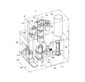
本発明を実施するための最良の形態において、基板処理装置は、一例として、半導体装置(IC)の製造方法における処理工程を実施する半導体製造装置として構成されている。尚、以下の説明では、基板処理装置として基板に酸化、拡散処理やCVD処理などを行う縦型の装置(以下、単に処理装置という)を適用した場合について述べる。図1には、本発明に適用される基板処理装置10が斜透視図を用いて示されている。また、図2には、基板処理装置10が側面透視図を用いて示されている。
Hereinafter, embodiments for carrying out the present invention will be described with reference to the drawings.
In the best mode for carrying out the present invention, as an example, the substrate processing apparatus is configured as a semiconductor manufacturing apparatus that performs processing steps in a method of manufacturing a semiconductor device (IC). In the following description, a case where a vertical apparatus (hereinafter simply referred to as a processing apparatus) that performs oxidation, diffusion processing, CVD processing, or the like is applied to the substrate as the substrate processing apparatus will be described. FIG. 1 shows a
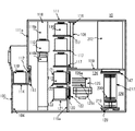
図1及び図2に示されているように、基板処理装置10は、基板として用いられるシリコン等からなるウエハ200を処理する。基板処理装置10では、ウエハ200を収納したウエハキャリアとして用いられるフープ(基板収容器、FOUPまたはポッドともいう。以下ポッドと記載する。)110が使用されている。また、基板処理装置10は、基板処理装置本体111を備えている。
As shown in FIGS. 1 and 2, the
基板処理装置本体111の正面壁111aの正面前方部にはメンテナンス可能なように設けられた開口部として用いられる正面メンテナンス口103が開設され、正面メンテナンス口103を開閉する正面メンテナンス扉104がそれぞれ建て付けられている。尚、図示しないが、上側の正面メンテナンス扉104近傍に副操作部としての副操作装置が設置される。主操作部としての主操作装置16は、背面側のメンテナンス扉近傍に配置される。
A
基板処理装置本体111の正面壁111aにはポッド搬入搬出口(基板収容器搬入搬出口)112が基板処理装置本体111の内外を連通するように開設されており、ポッド搬入搬出口112はフロントシャッタ(基板収容器搬入搬出口開閉機構)113によって開閉されるようになっている。
ポッド搬入搬出口112の正面前方側にはロードポート(基板収容器受渡し台)114が設置されており、ロードポート114はポッド110を載置されて位置合わせするように構成されている。ポッド110はロードポート114上に工程内搬送装置(図示せず)によって搬入され、ロードポート114上から搬出されるようになっている。
A pod loading / unloading port (substrate container loading / unloading port) 112 is established on the
A load port (substrate container delivery table) 114 is installed in front of the front side of the pod loading /
基板処理装置本体111内の前後方向の略中央部における上部には、回転式ポッド棚(基板収容器載置棚)105が設置されており、回転式ポッド棚105は複数個のポッド110を保管するように構成されている。すなわち、回転式ポッド棚105は垂直に立設されて水平面内で間欠回転される支柱116と、支柱116に上中下段の各位置において放射状に支持された複数枚の棚板(基板収容器載置台)117とを備えており、複数枚の棚板117はポッド110を複数個宛それぞれ載置した状態で保持するように構成されている。
A rotary pod shelf (substrate container mounting shelf) 105 is installed in an upper portion of the substrate processing apparatus
基板処理装置本体111内におけるロードポート114と回転式ポッド棚105との間には、ポッド搬送装置(基板収容器搬送装置)118が設置されており、ポッド搬送装置118は、ポッド110を保持したまま昇降可能なポッドエレベータ(基板収容器昇降機構)118aと搬送機構としてのポッド搬送機構(基板収容器搬送機構)118bとで構成されており、ポッド搬送装置118はポッドエレベータ118aとポッド搬送機構118bとの連続動作により、ロードポート114、回転式ポッド棚105、ポッドオープナ(基板収容器蓋体開閉機構)121との間で、ポッド110を搬送するように構成されている。
A pod transfer device (substrate container transfer device) 118 is installed between the
基板処理装置本体111内の前後方向の略中央部における下部には、サブ筐体119が後端にわたって構築されている。サブ筐体119の正面壁119aにはウエハ200をサブ筐体119内に対して搬入搬出するためのウエハ搬入搬出口(基板搬入搬出口)120が一対、垂直方向に上下二段に並べられて開設されており、上下段のウエハ搬入搬出口120、120には一対のポッドオープナ121、121がそれぞれ設置されている。ポッドオープナ121はポッド110を載置する載置台122、122と、ポッド110のキャップ(蓋体)を着脱するキャップ着脱機構(蓋体着脱機構)123、123とを備えている。ポッドオープナ121は載置台122に載置されたポッド110のキャップをキャップ着脱機構123によって着脱することにより、ポッド110のウエハ出し入れ口を開閉するように構成されている。
A
サブ筐体119はポッド搬送装置118や回転式ポッド棚105の設置空間から流体的に隔絶された移載室124を構成している。移載室124の前側領域にはウエハ移載機構(基板移載機構)125が設置されており、ウエハ移載機構125は、ウエハ200を水平方向に回転ないし直動可能なウエハ移載装置(基板移載装置)125a及びウエハ移載装置125aを昇降させるためのウエハ移載装置エレベータ(基板移載装置昇降機構)125bとで構成されている。図1に模式的に示されているようにウエハ移載装置エレベータ125bは耐圧基板処理装置本体111右側端部とサブ筐体119の移載室124前方領域右端部との間に設置されている。これら、ウエハ移載装置エレベータ125b及びウエハ移載装置125aの連続動作により、ウエハ移載装置125aのツイーザ(基板保持体)125cをウエハ200の載置部として、ボート(基板保持具)217に対してウエハ200を装填(チャージング)及び脱装(ディスチャージング)するように構成されている。
The
移載室124の後側領域には、ボート217を収容して待機させる待機部126が構成されている。待機部126の上方には、処理炉202が設けられている。処理炉202の下端部は、炉口シャッタ(炉口開閉機構)147により開閉されるように構成されている。
In the rear region of the
図1に模式的に示されているように、耐圧基板処理装置本体111右側端部とサブ筐体119の待機部126右端部との間にはボート217を昇降させるためのボートエレベータ(基板保持具昇降機構)115が設置されている。ボートエレベータ115の昇降台に連結された連結具としてのアーム128には蓋体としてのシールキャップ219が水平に据え付けられており、シールキャップ219はボート217を垂直に支持し、処理炉202の下端部を閉塞可能なように構成されている。
ボート217は複数本の保持部材を備えており、複数枚(例えば、50〜125枚程度)のウエハ200をその中心を揃えて垂直方向に整列させた状態で、それぞれ水平に保持するように構成されている。
As schematically shown in FIG. 1, a boat elevator (substrate holding) for raising and lowering the
The
また、図1に模式的に示されているように移載室124のウエハ移載装置エレベータ125b側及びボートエレベータ115側と反対側である左側端部には、清浄化した雰囲気もしくは不活性ガスであるクリーンエア133を供給するよう供給ファン及び防塵フィルタで構成されたクリーンユニット134が設置されており、ウエハ移載装置125aとクリーンユニット134との間には、図示はしないが、ウエハの円周方向の位置を整合させる基板整合装置としてのノッチ合わせ装置が設置されている。
Further, as schematically shown in FIG. 1, a clean atmosphere or inert gas is provided at the left end of the
クリーンユニット134から吹き出されたクリーンエア133は、ノッチ合わせ装置及びウエハ移載装置125a、待機部126にあるボート217に流通された後に、図示しないダクトにより吸い込まれて、基板処理装置本体111の外部に排気がなされるか、もしくはクリーンユニット134の吸い込み側である一次側(供給側)にまで循環され、再びクリーンユニット134によって、移載室124内に吹き出されるように構成されている。
なお、上述したクリーンエアの流れの経路を循環経路として説明する。
The clean air 133 blown out from the
The above-described clean air flow path will be described as a circulation path.
次に、本発明の基板処理装置10の動作について説明する。
図1及び図2に示されているように、ポッド110がロードポート114に供給されると、ポッド搬入搬出口112がフロントシャッタ113によって開放され、ロードポート114の上のポッド110はポッド搬送装置118によって基板処理装置本体111の内部へポッド搬入搬出口112から搬入される。
Next, the operation of the
As shown in FIGS. 1 and 2, when the
搬入されたポッド110は回転式ポッド棚105の指定された棚板117へポッド搬送装置118によって自動的に搬送されて受け渡され、一時的に保管された後、棚板117から一方のポッドオープナ121に搬送されて受け渡され、一時的に保管された後、棚板117から一方のポッドオープナ121に搬送されて載置台122に移載されるか、もしくは直接ポッドオープナ121に搬送されて載置台122に移載される。この際、ポッドオープナ121のウエハ搬入搬出口120はキャップ着脱機構123によって閉じられており、移載室124にはクリーンエア133が流通され、充満されている。例えば、移載室124にはクリーンエア133として窒素ガスが充満することにより、酸素濃度が20ppm以下と、基板処理装置本体111の内部(大気雰囲気)の酸素濃度よりも遥かに低く設定されている。
The loaded
載置台122に載置されたポッド110は、その開口側端面がサブ筐体119の正面壁119aにおけるウエハ搬入搬出口120の開口縁辺部に押し付けられるとともに、そのキャップがキャップ着脱機構123によって取り外され、ウエハ出し入れ口を開放される。
ポッド110がポッドオープナ121によって開放されると、ウエハ200はポッド110からウエハ移載装置125aのツイーザ125cによってウエハ出し入れ口を通じてピックアップされ、図示しないノッチ合わせ装置にてウエハを整合した後、移載室124の後方にある待機部126へ搬入され、ボート217に装填(チャージング)される。ボート217にウエハ200を受け渡したウエハ移載装置125aはポッド110に戻り、次のウエハをボート217に装填する。
The
When the
この一方(上段または下段)のポッドオープナ121におけるウエハ移載機構125によるウエハのボート217への装填作業中に、他方(下段または上段)のポッドオープナ121には回転式ポッド棚105から別のポッド110がポッド搬送装置118によって搬送されて移載され、ポッドオープナ121によるポッド110の開放作業が同時進行される。
During the loading operation of the wafer into the
予め指定された枚数のウエハ200がボート217に装填されると、炉口シャッタ147によって閉じられていた処理炉202の下端部が、炉口シャッタ147によって、開放される。続いて、ウエハ200群を保持したボート217はシールキャップ219がボートエレベータ115によって上昇されることにより、処理炉202内へ搬入(ローディング)されていく。
When a predetermined number of
ローディング後は、処理炉202にてウエハ200に任意の処理が実施される。
処理後は、図示しないノッチ合わせ装置でのウエハの整合工程を除き、概上述の逆の手順で、ウエハ200及びポッド110は筐体の外部へ払い出される。
After loading, arbitrary processing is performed on the
After the processing, the
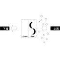
次に、図3を参照して、第一の実施形態である基板処理装置10の移載室124における循環エアーの流れについて説明する。
図3に示されるように、クリーンユニット134に供給される高純度の不活性ガスは、第一のクリーンユニット134に具備されたフィルタを通過してボート217方向へ流れる。その後、ボート217やボートエレベータ115の駆動部やウエハ移載機構(基板移載機構)125、図示しない基板搬送装置といったパーティクル等の発生源である発塵源を通過し、移載室124に設けられた第一のクリーンユニット134が設置されている側壁と対向する側壁に、設けられた小型の第二のクリーンユニット134−2、第三のクリーンユニット134−3を通過することによって、フィルタにより清浄化された不活性ガスが循環経路を通過して、第一のクリーンユニット134に戻ることにより、常にクリーンな不活性ガスが循環することとなる。このように、本発明は、循環経路中のボートやボートエレベータといった発塵源の前後(上下流)にクリーンユニットを設けることを特徴としている。
Next, the flow of circulating air in the
As shown in FIG. 3, the high purity inert gas supplied to the
なお、ここでクリーンユニット134、134−2、134−3といったクリーンユニットの構成は、図4に示すように、ファンとフィルタ部から構成されている。すべてのクリーンユニットにファンが搭載されている必要はないが、ファンがあることによって、圧力損失が少なく、正常なエアーの循環が可能となるため、ファンを有していたほうがより良い。単純にフィルタだけを循環経路に複数増やした場合には、各フィルタで圧力損失が起き、正常なエアーの循環の妨げとなってしまう。従来は、クリーンユニット134のみにファンを有しており、エアー循環路中には、他のクリーンユニットを設けていなかったが、本発明においては、循環路中のクリーンユニットにもファンを設けてあることにより、エアーの循環路中のよどみ部に残っている微小パーティクルに流れを作ることができ、フィルタリングが可能となるというメリットが生じる。
Here, the configuration of the clean units such as the
以上説明したように、本願発明の第一の実施形態は、基板処理装置の移載室内のエアーの循環路中の発塵源となるボートやボートエレベータの前後にファンとフィルタから構成されるクリーンユニットを設けた点に特徴がある。 As described above, the first embodiment of the present invention is a clean unit composed of a fan and a filter before and after a boat or a boat elevator that is a dust generation source in the air circulation path in the transfer chamber of the substrate processing apparatus. It is characterized in that a unit is provided.
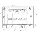
次に本発明の第二の実施形態を図5を用いて説明する。この第二の実施形態では、半導体製造装置(基板処理装置)のプラントに応用するものである。図5に示すように、プラント500は、上部クリーンユニット501と基板処理装置111と構成される下部クリーンユニット502とエアー循環路503とから構成されている。なお、上部クリーンユニット501及び下部クリーンユニット502はそれぞれ上部供給ファンと上部防塵フィルタ、及び下部供給ファンと下部防塵フィルタから構成されているものである。本実施の形態の場合も、発塵源である基板処理装置111の前後(上下流)にクリーンユニット501、502を設けることにより、プラント内のエアーの清浄度を保つことが可能となる。
Next, a second embodiment of the present invention will be described with reference to FIG. In the second embodiment, the present invention is applied to a semiconductor manufacturing apparatus (substrate processing apparatus) plant. As shown in FIG. 5, the plant 500 includes a lower
本発明によれば、高純度不活性ガスの使用量を抑えることができ、環境配慮型の省エネルギー効果が得られる。また、常にクリーン度を要求される半導体製造装置筐体内の不活性ガスの循環が効率良く行うことができると共に、自然酸化膜の抑制や基板処理装置筐体内のO2濃度を短時間で下げることができ、生産性の向上につながる効果が得られる。 According to the present invention, the amount of high-purity inert gas used can be suppressed, and an environment-friendly energy saving effect can be obtained. In addition, it is possible to efficiently circulate the inert gas in the semiconductor manufacturing apparatus casing that always requires cleanliness, and to suppress the natural oxide film and reduce the O 2 concentration in the substrate processing apparatus casing in a short time. Can be obtained, and the effect of improving productivity can be obtained.
また、本発明によれば、フィルタとファンを具備したクリーンモジュールを移載室内のエアーの循環経路に2つ以上配置し、クリーンな不活性ガスを溜まり無く効率的に循環させることによって、従来より少ない不活性ガスの供給で、常に循環効率良く、O2濃度を低減することができる。また、クリーンモジュールの数は上から下への流れや、左右方向など数は限定しない。よどみの発生する箇所にはあらかじめ循環経路へ流れるようにクリーンモジュールを配置することにより、パーティクルの除去に効果がある。 In addition, according to the present invention, two or more clean modules equipped with a filter and a fan are arranged in the air circulation path in the transfer chamber, and the clean inert gas is efficiently circulated without accumulating. By supplying a small amount of inert gas, it is possible to always reduce the O 2 concentration with good circulation efficiency. Also, the number of clean modules is not limited, such as the flow from top to bottom or the left-right direction. Placing a clean module in advance so that the stagnation occurs in the circulation path is effective in removing particles.
なお、以上は本発明の好ましい実施形態を述べたに過ぎず、本発明は上記実施形態に限定されるものではなく、その要旨を逸脱しない範囲で種々変更可能である。
例えば、本発明は、基板処理装置10として、例えば、半導体装置(IC)の製造方法を実施する半導体製造装置として説明したが、半導体製造装置だけでなくLCD装置のようなガラス基板を処理する装置にも適用することができる。
Note that the above is only a preferred embodiment of the present invention, and the present invention is not limited to the above embodiment, and various modifications can be made without departing from the scope of the present invention.
For example, although the present invention has been described as the
基板処理装置10で行われる成膜処理には、例えば、CVD、PVD、ALD、Epi、その他酸化膜、窒化膜を形成する処理、金属を含む膜を形成する処理がある。更に、アニール処理、酸化処理、拡散処理等の処理でも構わない。
また、本実施形態では、基板処理装置が縦型処理装置10であるとして記載したが、枚葉装置についても同様に適用することができ、さらに、エッチング装置、露光装置、リソグラフィ装置、塗布装置、モールド装置、現像装置、ダイシング装置、ワイヤボンディング装置、検査装置等にも同様に適用することができる。
Examples of the film forming process performed in the
In the present embodiment, the substrate processing apparatus is described as the
<本発明の好ましい態様>
以下に、本発明の好ましい態様について付記する。
<Preferred embodiment of the present invention>
Hereinafter, preferred embodiments of the present invention will be additionally described.
(付記1)
基板を処理する処理室と、
該処理室に隣接する基板移載空間を構成する移載室と、
前記移載室に対し吹出口から気体を吹き出すファンとフィルタから構成される第一のクリーンユニットと、
前記第一のクリーンユニットの吹出口より下流側に配置されるファンとフィルタから構成される第二のクリーンユニットと、
前記第一のクリーンユニットと第二のクリーンユニットに接続され、前記移載室内の雰囲気を循環させる循環経路と、を備え、
前記第二のクリーンユニットから前記循環経路を通り前記気体が前記第一のクリーンユニットに戻るように構成される基板処理装置。
(Appendix 1)
A processing chamber for processing the substrate;
A transfer chamber constituting a substrate transfer space adjacent to the processing chamber;
A first clean unit composed of a fan and a filter that blows gas from a blowout port to the transfer chamber;
A second clean unit composed of a fan and a filter disposed on the downstream side of the outlet of the first clean unit;
A circulation path connected to the first clean unit and the second clean unit and circulating the atmosphere in the transfer chamber;
A substrate processing apparatus configured to return the gas from the second clean unit through the circulation path to the first clean unit.
(付記2)
付記1に記載の基板処理装置であって、
前記第二のクリーンユニットの吹出口より下流側に配置され、前記循環経路に接続されるファンとフィンから構成される第三のクリーンユニットを有する基板処理装置。
(Appendix 2)
The substrate processing apparatus according to appendix 1, wherein
The substrate processing apparatus which has a 3rd clean unit which is arrange | positioned downstream from the blower outlet of said 2nd clean unit, and is comprised from the fan and fin which are connected to the said circulation path.
(付記3)
付記1または2に記載の基板処理装置であって、
前記第1のクリーンユニットと前記第2のクリーンユニットは前記移載室の対向する側壁にそれぞれ設けられている基板処理装置。
(Appendix 3)
The substrate processing apparatus according to appendix 1 or 2, wherein
The substrate processing apparatus, wherein the first clean unit and the second clean unit are respectively provided on opposite side walls of the transfer chamber.
(付記4)
付記1から3のいずれか1つに記載の基板処理装置を複数設置した基板処理プラントであって、
前記基板処理プラントは、プラント上部に前記基板処理装置に対し吹出口から気体を吹き出す上部供給ファンと上部防塵フィルタから構成される上部クリーンユニットと、
基板処理装置の下部に設置され、前記上部クリーンユニットより供給された気体を吸気し、方向を変えて供給する下部供給ファンと、下部防塵フィルタで構成される下部クリーンユニットを有する基板処理プラント。
(Appendix 4)
A substrate processing plant in which a plurality of substrate processing apparatuses according to any one of appendices 1 to 3 are installed,
The substrate processing plant is an upper clean unit composed of an upper supply fan and an upper dustproof filter that blows gas from a blower outlet to the substrate processing apparatus at the upper part of the plant,
A substrate processing plant having a lower clean unit, which is installed at a lower portion of a substrate processing apparatus and sucks in gas supplied from the upper clean unit and supplies the gas in a changed direction and a lower clean unit.
(付記5)
基板を処理する基板の処理方法であって、
基板処理室に隣接する移載室内に対し、ファンとフィルタから構成される第一のクリーンユニットから気体を吹き出すステップと、
前記気体が下流側に配置されるファンとフィルタから構成される前記第二のクリーンユニットを通過するステップと、
前記第二のクリーンユニットから循環経路を通り前記気体が前記第一のクリーンユニットに戻るステップと
を有する基板処理方法。
(Appendix 5)
A substrate processing method for processing a substrate, comprising:
Blowing gas from the first clean unit composed of a fan and a filter to the transfer chamber adjacent to the substrate processing chamber;
The gas passes through the second clean unit comprising a fan and a filter disposed downstream;
And a step of returning the gas to the first clean unit through a circulation path from the second clean unit.
(付記6)
付記1の基板処理装置を用いて処理する半導体装置の製造方法であって、
前記第一のクリーンユニットから気体を吹き出すステップと、
前記気体が前記発塵源を通過するステップと、
前記発塵源を通過した気体が前記第二のクリーンユニットを通過するステップと、
前記第二のクリーンユニットを通過した前記気体が前記循環経路を通り前記気体が前記第一のクリーンユニットに戻るステップと、
を有する半導体装置の製造方法。
(Appendix 6)
A method for manufacturing a semiconductor device to be processed using the substrate processing apparatus of appendix 1,
Blowing out gas from the first clean unit;
Passing the gas through the dust source;
A gas passing through the dust generation source passes through the second clean unit;
The step of passing the gas through the second clean unit through the circulation path and returning the gas to the first clean unit;
A method for manufacturing a semiconductor device comprising:
(付記7)
基板を処理する半導体装置の製造方法であって、
基板処理室に隣接する移載室内に対し、ファンとフィルタから構成される第一のクリーンユニットから気体を吹き出すステップと、
前記気体が下流側に配置されるファンとフィルタから構成される前記第二のクリーンユニットを通過するステップと、
前記第二のクリーンユニットから循環経路を通り前記気体が前記第一のクリーンユニットに戻るステップと
を有する半導体装置の製造方法。
(Appendix 7)
A method of manufacturing a semiconductor device for processing a substrate,
Blowing gas from the first clean unit composed of a fan and a filter to the transfer chamber adjacent to the substrate processing chamber;
The gas passes through the second clean unit comprising a fan and a filter disposed downstream;
And a step of returning the gas to the first clean unit through a circulation path from the second clean unit.
10 基板処理装置、
115 ボートエレベータ、
124 移載室、
134 第一のクリーンユニット、
134−2 第二のクリーンユニット、
134−3 第三のクリーンユニット、
200 ウエハ、
202 処理室、
217 ボート、
500 プラント。
10 substrate processing apparatus,
115 boat elevators,
124 Transfer room,
134 The first clean unit,
134-2 Second clean unit,
134-3 The third clean unit,
200 wafers,
202 treatment chamber,
217 boat,
500 plant.
Claims (3)
該処理室に隣接する基板移載空間を構成する移載室と、
前記移載室に対し吹出口から気体を吹き出すファンとフィルタから構成される第一のクリーンユニットと、
前記第一のクリーンユニットの吹出口より下流側に配置されるファンとフィルタから構成される第二のクリーンユニットと、
前記第一のクリーンユニットと第二のクリーンユニットに接続され、前記移載室内の雰囲気を循環させる循環経路と、を備え、
前記第二のクリーンユニットから前記循環経路を通り前記気体が前記第一のクリーンユニットに戻るように構成される基板処理装置。 A processing chamber for processing the substrate;
A transfer chamber constituting a substrate transfer space adjacent to the processing chamber;
A first clean unit composed of a fan and a filter that blows gas from a blowout port to the transfer chamber;
A second clean unit composed of a fan and a filter disposed on the downstream side of the outlet of the first clean unit;
A circulation path connected to the first clean unit and the second clean unit and circulating the atmosphere in the transfer chamber;
A substrate processing apparatus configured to return the gas from the second clean unit through the circulation path to the first clean unit.
基板処理室に隣接する移載室内に対し、ファンとフィルタから構成される第一のクリーンユニットから気体を吹き出すステップと、
前記気体が下流側に配置されるファンとフィルタから構成される前記第二のクリーンユニットを通過するステップと、
前記第一のクリーンユニットと第二のクリーンユニットに接続された循環経路によって、前記第二のクリーンユニットから吹き出された気体が前記循環経路を通り前記気体が前記第一のクリーンユニットに戻るステップと、
を有する基板処理方法。 A substrate processing method for processing a substrate, comprising:
Blowing gas from the first clean unit composed of a fan and a filter to the transfer chamber adjacent to the substrate processing chamber;
The gas passes through the second clean unit comprising a fan and a filter disposed downstream;
A gas blown out of the second clean unit through the circulation path by the circulation path connected to the first clean unit and the second clean unit; and the gas returns to the first clean unit; ,
A substrate processing method.
基板処理室に隣接する移載室内に対し、ファンとフィルタから構成される第一のクリーンユニットから気体を吹き出すステップと、
前記気体が下流側に配置されるファンとフィルタから構成される前記第二のクリーンユニットを通過するステップと、
前記第一のクリーンユニットと第二のクリーンユニットに接続された循環経路によって、前記第二のクリーンユニットから吹き出された気体が循環経路を通り前記気体が前記第一のクリーンユニットに戻るステップと、
を有する半導体装置の製造方法。
A method of manufacturing a semiconductor device for processing a substrate,
Blowing gas from the first clean unit composed of a fan and a filter to the transfer chamber adjacent to the substrate processing chamber;
The gas passes through the second clean unit comprising a fan and a filter disposed downstream;
The gas blown out of the second clean unit through the circulation path connected to the first clean unit and the second clean unit through the circulation path, and the gas returns to the first clean unit;
A method for manufacturing a semiconductor device comprising:
Priority Applications (1)
| Application Number | Priority Date | Filing Date | Title |
|---|---|---|---|
| JP2012210759A JP2014067797A (en) | 2012-09-25 | 2012-09-25 | Substrate processing apparatus, substrate processing method and semiconductor device manufacturing method |
Applications Claiming Priority (1)
| Application Number | Priority Date | Filing Date | Title |
|---|---|---|---|
| JP2012210759A JP2014067797A (en) | 2012-09-25 | 2012-09-25 | Substrate processing apparatus, substrate processing method and semiconductor device manufacturing method |
Publications (2)
| Publication Number | Publication Date |
|---|---|
| JP2014067797A true JP2014067797A (en) | 2014-04-17 |
| JP2014067797A5 JP2014067797A5 (en) | 2015-11-12 |
Family
ID=50743923
Family Applications (1)
| Application Number | Title | Priority Date | Filing Date |
|---|---|---|---|
| JP2012210759A Pending JP2014067797A (en) | 2012-09-25 | 2012-09-25 | Substrate processing apparatus, substrate processing method and semiconductor device manufacturing method |
Country Status (1)
| Country | Link |
|---|---|
| JP (1) | JP2014067797A (en) |
Cited By (3)
| Publication number | Priority date | Publication date | Assignee | Title |
|---|---|---|---|---|
| JP2017112137A (en) * | 2015-12-14 | 2017-06-22 | Tdk株式会社 | Mini-environment device |
| CN107504557A (en) * | 2017-07-14 | 2017-12-22 | 太仓诚泽网络科技有限公司 | Indoor air cleaning system |
| US11342201B2 (en) | 2019-03-28 | 2022-05-24 | SCREEN Holdings Co., Ltd. | Substrate processing apparatus |
Citations (7)
| Publication number | Priority date | Publication date | Assignee | Title |
|---|---|---|---|---|
| JPH05226456A (en) * | 1992-02-17 | 1993-09-03 | Dainippon Screen Mfg Co Ltd | Structure for mounting clean air unit of vertical substrate heat treatment device |
| JPH06302679A (en) * | 1993-04-13 | 1994-10-28 | Tokyo Electron Ltd | Material-to-be-treated conveying box and treating apparatus |
| JPH06318553A (en) * | 1993-04-30 | 1994-11-15 | Tokyo Electron Ltd | Heat treating apparatus |
| JPH07283288A (en) * | 1994-04-07 | 1995-10-27 | Tokyo Electron Ltd | Processing device |
| JPH1092760A (en) * | 1996-09-09 | 1998-04-10 | Tokyo Electron Ltd | Heat treatment device |
| JPH10267338A (en) * | 1997-03-21 | 1998-10-09 | Sanki Eng Co Ltd | Clean room |
| US20070141851A1 (en) * | 2005-12-16 | 2007-06-21 | Selen Louis J | System and method of reducing particle contamination of semiconductor substrates |
-
2012
- 2012-09-25 JP JP2012210759A patent/JP2014067797A/en active Pending
Patent Citations (7)
| Publication number | Priority date | Publication date | Assignee | Title |
|---|---|---|---|---|
| JPH05226456A (en) * | 1992-02-17 | 1993-09-03 | Dainippon Screen Mfg Co Ltd | Structure for mounting clean air unit of vertical substrate heat treatment device |
| JPH06302679A (en) * | 1993-04-13 | 1994-10-28 | Tokyo Electron Ltd | Material-to-be-treated conveying box and treating apparatus |
| JPH06318553A (en) * | 1993-04-30 | 1994-11-15 | Tokyo Electron Ltd | Heat treating apparatus |
| JPH07283288A (en) * | 1994-04-07 | 1995-10-27 | Tokyo Electron Ltd | Processing device |
| JPH1092760A (en) * | 1996-09-09 | 1998-04-10 | Tokyo Electron Ltd | Heat treatment device |
| JPH10267338A (en) * | 1997-03-21 | 1998-10-09 | Sanki Eng Co Ltd | Clean room |
| US20070141851A1 (en) * | 2005-12-16 | 2007-06-21 | Selen Louis J | System and method of reducing particle contamination of semiconductor substrates |
Cited By (3)
| Publication number | Priority date | Publication date | Assignee | Title |
|---|---|---|---|---|
| JP2017112137A (en) * | 2015-12-14 | 2017-06-22 | Tdk株式会社 | Mini-environment device |
| CN107504557A (en) * | 2017-07-14 | 2017-12-22 | 太仓诚泽网络科技有限公司 | Indoor air cleaning system |
| US11342201B2 (en) | 2019-03-28 | 2022-05-24 | SCREEN Holdings Co., Ltd. | Substrate processing apparatus |
Similar Documents
| Publication | Publication Date | Title |
|---|---|---|
| JP4763841B2 (en) | Substrate processing apparatus and semiconductor device manufacturing method | |
| JP5779957B2 (en) | Loading unit and processing system | |
| TW200816299A (en) | Liquid processing system | |
| JP2013033965A (en) | Substrate processing apparatus, substrate processing facility, and substrate processing method | |
| JP2009010009A (en) | Substrate processing apparatus and fabrication process of semiconductor device | |
| KR101400157B1 (en) | Apparatus, system and method for treating substrate | |
| TWI702383B (en) | Container mounting device, semiconductor manufacturing device, and method for controlling ambient gas in the container | |
| JP2007095879A (en) | Substrate processing equipment | |
| KR101740613B1 (en) | Substrate processing apparatus, substrate processing method, and semiconductor device manufacturing method | |
| JP2014067797A (en) | Substrate processing apparatus, substrate processing method and semiconductor device manufacturing method | |
| JP2020113746A (en) | Processing apparatus | |
| JP2009266962A (en) | Substrate processing apparatus and method for manufacturing semiconductor device | |
| JP2015167240A (en) | Substrate processing apparatus and semiconductor device manufacturing method | |
| JP5164416B2 (en) | Substrate processing apparatus, storage container transport method, and semiconductor device manufacturing method | |
| JP2004119888A (en) | Semiconductor manufacturing apparatus | |
| JP2012054392A (en) | Substrate processing apparatus and semiconductor manufacturing method | |
| JP2011243677A (en) | Substrate processing device | |
| JP2019091753A (en) | Load port device | |
| JP3856726B2 (en) | Semiconductor manufacturing equipment | |
| JP2005347667A (en) | Semiconductor fabrication device | |
| JP2011044633A (en) | Substrate processing apparatus | |
| JP2004119627A (en) | Semiconductor device manufacturing apparatus | |
| JP7209503B2 (en) | SUBSTRATE PROCESSING APPARATUS AND SUBSTRATE PROCESSING METHOD | |
| JP4322411B2 (en) | Semiconductor manufacturing equipment | |
| JP2007242789A (en) | Substrate processor |
Legal Events
| Date | Code | Title | Description |
|---|---|---|---|
| A521 | Written amendment |
Free format text: JAPANESE INTERMEDIATE CODE: A523 Effective date: 20150918 |
|
| A621 | Written request for application examination |
Free format text: JAPANESE INTERMEDIATE CODE: A621 Effective date: 20150918 |
|
| A977 | Report on retrieval |
Free format text: JAPANESE INTERMEDIATE CODE: A971007 Effective date: 20160818 |
|
| A131 | Notification of reasons for refusal |
Free format text: JAPANESE INTERMEDIATE CODE: A131 Effective date: 20160825 |
|
| A521 | Written amendment |
Free format text: JAPANESE INTERMEDIATE CODE: A523 Effective date: 20161021 |
|
| A02 | Decision of refusal |
Free format text: JAPANESE INTERMEDIATE CODE: A02 Effective date: 20161215 |