JP2014041282A - Liquid crystal display device - Google Patents
Liquid crystal display device Download PDFInfo
- Publication number
- JP2014041282A JP2014041282A JP2012184023A JP2012184023A JP2014041282A JP 2014041282 A JP2014041282 A JP 2014041282A JP 2012184023 A JP2012184023 A JP 2012184023A JP 2012184023 A JP2012184023 A JP 2012184023A JP 2014041282 A JP2014041282 A JP 2014041282A
- Authority
- JP
- Japan
- Prior art keywords
- substrate
- liquid crystal
- spacer
- crystal display
- base resin
- Prior art date
- Legal status (The legal status is an assumption and is not a legal conclusion. Google has not performed a legal analysis and makes no representation as to the accuracy of the status listed.)
- Pending
Links
Images


Classifications
-
- G—PHYSICS
- G02—OPTICS
- G02F—OPTICAL DEVICES OR ARRANGEMENTS FOR THE CONTROL OF LIGHT BY MODIFICATION OF THE OPTICAL PROPERTIES OF THE MEDIA OF THE ELEMENTS INVOLVED THEREIN; NON-LINEAR OPTICS; FREQUENCY-CHANGING OF LIGHT; OPTICAL LOGIC ELEMENTS; OPTICAL ANALOGUE/DIGITAL CONVERTERS
- G02F1/00—Devices or arrangements for the control of the intensity, colour, phase, polarisation or direction of light arriving from an independent light source, e.g. switching, gating or modulating; Non-linear optics
- G02F1/01—Devices or arrangements for the control of the intensity, colour, phase, polarisation or direction of light arriving from an independent light source, e.g. switching, gating or modulating; Non-linear optics for the control of the intensity, phase, polarisation or colour
- G02F1/13—Devices or arrangements for the control of the intensity, colour, phase, polarisation or direction of light arriving from an independent light source, e.g. switching, gating or modulating; Non-linear optics for the control of the intensity, phase, polarisation or colour based on liquid crystals, e.g. single liquid crystal display cells
- G02F1/133—Constructional arrangements; Operation of liquid crystal cells; Circuit arrangements
- G02F1/1333—Constructional arrangements; Manufacturing methods
- G02F1/1339—Gaskets; Spacers; Sealing of cells
- G02F1/13394—Gaskets; Spacers; Sealing of cells spacers regularly patterned on the cell subtrate, e.g. walls, pillars
-
- G—PHYSICS
- G02—OPTICS
- G02F—OPTICAL DEVICES OR ARRANGEMENTS FOR THE CONTROL OF LIGHT BY MODIFICATION OF THE OPTICAL PROPERTIES OF THE MEDIA OF THE ELEMENTS INVOLVED THEREIN; NON-LINEAR OPTICS; FREQUENCY-CHANGING OF LIGHT; OPTICAL LOGIC ELEMENTS; OPTICAL ANALOGUE/DIGITAL CONVERTERS
- G02F1/00—Devices or arrangements for the control of the intensity, colour, phase, polarisation or direction of light arriving from an independent light source, e.g. switching, gating or modulating; Non-linear optics
- G02F1/01—Devices or arrangements for the control of the intensity, colour, phase, polarisation or direction of light arriving from an independent light source, e.g. switching, gating or modulating; Non-linear optics for the control of the intensity, phase, polarisation or colour
- G02F1/13—Devices or arrangements for the control of the intensity, colour, phase, polarisation or direction of light arriving from an independent light source, e.g. switching, gating or modulating; Non-linear optics for the control of the intensity, phase, polarisation or colour based on liquid crystals, e.g. single liquid crystal display cells
- G02F1/133—Constructional arrangements; Operation of liquid crystal cells; Circuit arrangements
- G02F1/1333—Constructional arrangements; Manufacturing methods
- G02F1/1341—Filling or closing of cells
Abstract
Description
本発明の実施形態は、液晶表示装置に関する。 Embodiments described herein relate generally to a liquid crystal display device.
現在、一般的に用いられている液晶表示素子は、電極を有する二枚のガラス基板の間に液晶を挟持し、二枚の基板の周囲が接着剤で固定された構成をしている。 Currently, a liquid crystal display element generally used has a configuration in which a liquid crystal is sandwiched between two glass substrates having electrodes, and the periphery of the two substrates is fixed with an adhesive.
カラー型アクティブマトリクス駆動液晶表示素子は、例えば、ポリシリコン(p−Si)を半導体層とした薄膜トランジスタ(TFT)とそれに接続された表示電極と信号線電極、ゲート電極が形成されたアクティブマトリクス基板であるTFTアレイ基板と、対向電極とRGBカラーフィルタが形成された対向基板とを基板周辺に配置した接着剤にて張り合わせ、その間に液晶組成物を挟持した構成を有する。このカラー型アクティブマトリクス駆動液晶表示素子においては、この二枚の基板の両側に偏光板を挟持させ、光シャッターとして使用して、カラー画像を表示している。 The color type active matrix driving liquid crystal display element is, for example, an active matrix substrate in which a thin film transistor (TFT) using polysilicon (p-Si) as a semiconductor layer, a display electrode connected thereto, a signal line electrode, and a gate electrode are formed. A TFT array substrate and a counter substrate on which a counter electrode and an RGB color filter are formed are bonded together with an adhesive disposed around the substrate, and a liquid crystal composition is sandwiched therebetween. In this color type active matrix drive liquid crystal display element, a polarizing plate is sandwiched between both sides of the two substrates and used as an optical shutter to display a color image.
カラーフィルタの各色層の間と額縁部には遮光層が設けられており、パターニング精度に起因してや光漏れや混色が起きることを防止するため、遮光層の上に色層が乗り上げる構造になっている。 A light-shielding layer is provided between the color layers of the color filter and in the frame, and the color layer rides on the light-shielding layer to prevent light leakage and color mixing due to patterning accuracy. Yes.
二枚の基板間の距離を一定に保つためのスペーサーとして粒径の均一なプラスティックビーズ等を基板間に散在させる従来の方法に代わり、近年は、突起物を一方の基板上の形成する方法が用いられている。この方法は、スペーサーの選択的配置と高さの精度向上によるギャップ均一化に有効である。 In recent years, instead of the conventional method in which plastic beads having a uniform particle size are scattered between the substrates as a spacer for keeping the distance between the two substrates constant, there is a method of forming protrusions on one substrate. It is used. This method is effective for uniform gaps by selectively arranging spacers and improving height accuracy.
ギャップ均一化には、二枚の基板を貼り合わせる方法も重要である。 A method of bonding two substrates together is also important for uniforming the gap.
アレイ基板、対向基板のいずれか一方の液晶注入口を除く周辺部に配置した接着剤で二枚の基板を張り合わせた後に荷重をかけるか、あるいは真空にして液晶注入口から基板間の空気を抜きながら接着剤を潰しギャップを形成する方法と、いずれか一方の基板上の接着剤で囲まれた領域内に液晶を所定量滴下した状態で、二枚の基板を真空状態で貼り合わせた後に、真空状態から大気圧状態に戻し、基板間の接着剤より内側の領域と外気との圧力差によって接着剤が潰れ、基板間に所定のギャップを形成させる方法とがある。後者は滴下注入と呼ばれ、タクトタイム短縮、材料の利用効率向上、高いギャップ精度の観点から液晶注入・組立ての方式として広く普及している。 Apply the load after bonding the two substrates with the adhesive placed in the peripheral area excluding the liquid crystal injection port of either the array substrate or the counter substrate, or evacuate the air between the substrates from the liquid crystal injection port While crushing the adhesive and forming a gap, in a state where a predetermined amount of liquid crystal is dropped in a region surrounded by the adhesive on one of the substrates, after bonding the two substrates in a vacuum state, There is a method in which the vacuum state is returned to the atmospheric pressure state, the adhesive is crushed by a pressure difference between the region inside the adhesive between the substrates and the outside air, and a predetermined gap is formed between the substrates. The latter is called drop injection, and is widely used as a liquid crystal injection / assembly method from the viewpoints of shortening tact time, improving material utilization efficiency, and high gap accuracy.
後者の製造方法において、一般に接着剤領域には、スペーサーが配置されている。これにより、真空状態から大気圧状態に戻した際に接着剤部の過度な潰れを防ぐことができ、表示領域へのセル歪を抑制することができる。 In the latter manufacturing method, a spacer is generally disposed in the adhesive region. Thereby, when the vacuum state is returned to the atmospheric pressure state, excessive crushing of the adhesive portion can be prevented, and cell distortion to the display region can be suppressed.
この滴下する液晶量のバラツキや、セル内容積のバラツキが想定され、液晶過多もしくは過少の場合に表示不良が発生する。 A variation in the amount of liquid crystal to be dropped and a variation in the internal volume of the cell are assumed, and a display defect occurs when the liquid crystal is excessive or insufficient.
特に液晶過多の場合は、アレイ基板と対向基板を貼り合わせた際のセル形状を反映した表示不良が発生する。 In particular, when the liquid crystal is excessive, a display defect reflecting the cell shape when the array substrate and the counter substrate are bonded together occurs.
例えば、表示領域に対して、接着剤の領域のセル厚が十分に厚い場合、セル断面は鼓型となる。液晶過多の場合は、セルが厚い領域に液晶が溜まるため、周辺ギャップムラ(周辺部が黄色く色付く)として視認される。一方、接着剤領域が潰れセルが薄くなっている場合、セルは太鼓腹型となる。液晶過多の場合は、表示領域に液晶が溜まりムラとして視認される。やや液晶が過多の場合でも、セルを立てた状態で加温した場合に、中央部の液晶が自重により下側に移動して溜まり、下辺部近傍がムラ(重力ムラ)として視認される。 For example, when the cell thickness of the adhesive region is sufficiently thick with respect to the display region, the cell cross section has a drum shape. When the liquid crystal is excessive, the liquid crystal accumulates in a region where the cells are thick, so that it is visually recognized as peripheral gap unevenness (peripheral portion is colored yellow). On the other hand, when the adhesive region is crushed and the cell is thin, the cell becomes a paunch type. In the case of excessive liquid crystal, liquid crystal accumulates in the display area and is visually recognized as unevenness. Even when the liquid crystal is excessively large, when the cell is heated in a standing state, the liquid crystal at the center moves downward due to its own weight and accumulates, and the vicinity of the lower side is visually recognized as unevenness (gravity unevenness).
この接着剤領域は、接着剤と基板の密着性を向上するために、接着剤と接する基板上の下地樹脂膜の一部をパターン抜き取りし、接着剤と例えば無機膜が直接接触する一定の面積を確保する方法がある。 In order to improve the adhesiveness between the adhesive and the substrate, this adhesive region is a certain area in which a part of the base resin film on the substrate in contact with the adhesive is extracted to directly contact the adhesive and the inorganic film, for example. There is a way to ensure.
また、狭額縁化の要求が進むにつれ、接着剤領域幅を狭くする傾向がある中、接着剤と無機膜の接触に一定面積を確保するとなると、接着剤領域中のスペーサー配置に制約が生ずる。 Further, as the demand for narrowing the frame advances, the width of the adhesive region tends to be narrowed. If a certain area is secured for the contact between the adhesive and the inorganic film, the arrangement of the spacers in the adhesive region is restricted.
また、このスペーサーは、表示領域のアレイ基板と対向基板の間隙を形成するスペーサーと同時形成されるが、下地となる樹脂膜のパターン端にスペーサーを形成した場合、レベリングにより表示領域のスペーサーに比べて低くなる傾向がある。 This spacer is formed at the same time as the spacer that forms the gap between the array substrate in the display area and the counter substrate. However, if the spacer is formed at the pattern edge of the resin film that is the base, leveling will cause a comparison with the spacer in the display area. Tend to be low.
樹脂膜のパターン端に形成したスペーサー高さは、下地樹脂膜の抜き取り幅に依存する。アレイ基板側の実装部は樹脂膜が抜き取られているため、トータルの樹脂膜抜き取り幅が最も広くなる。その結果、実装辺の樹脂膜のパターン端に形成されるスペーサーは他辺に比べてさらに低くなる。その結果、表示領域のスペーサーに比べて実装部の接着剤領域のスペーサーは著しく低くなる傾向がある。 The height of the spacer formed at the pattern edge of the resin film depends on the extraction width of the base resin film. Since the resin film is extracted from the mounting portion on the array substrate side, the total resin film extraction width is the widest. As a result, the spacer formed at the pattern end of the resin film on the mounting side is further lower than the other side. As a result, the spacer in the adhesive region of the mounting portion tends to be significantly lower than the spacer in the display region.
このような液晶表示装置を、実装辺を下側にして立て掛けた場合、加温時に重力ムラが発生する課題がある。 When such a liquid crystal display device is stood with its mounting side down, there is a problem that uneven gravity occurs during heating.
本発明の実施形態は、重力ムラによる画像品質の低下を抑制することを目的とする。 An embodiment of the present invention aims to suppress a decrease in image quality due to gravity unevenness.
実施形態によれば、 第1の基板、該第1の基板の一主面上に形成された下地樹脂層、及び該下地樹脂層上にマトリクス状に形成されて表示領域を構成する複数の画素電極、及び該第1の基板の一主面上に該下地樹脂層と間隔をおいて実装されたICを含むアレイ基板と、
該アレイ基板に対向して設けられ、第2の基板、及び該第2の基板上に形成され、該表示領域周囲の周辺領域を遮蔽する遮光層を含む対向基板と、
該アレイ基板と該対向基板とを該周辺領域において接着するシール材と、
該下地樹脂層上の該周辺領域に形成され、該シール材中に設けられた複数のスペーサーと、
該アレイ基板と該対向基板とシール材とにより区画された領域に封入された液晶とを具備する液晶表示装置であって、
前記シール材において、前記ICに隣接する実装辺に設けられたスペーサーを対向基板側から見た場合の面密度は、その他の辺に設けられたスペーサーの面密度に比べて高いことを特徴とする液晶表示装置が提供される。
According to the embodiment, a first substrate, a base resin layer formed on one main surface of the first substrate, and a plurality of pixels formed in a matrix on the base resin layer and constituting a display region An array substrate including an electrode and an IC mounted on one main surface of the first substrate at a distance from the base resin layer;
A counter substrate provided opposite to the array substrate, including a second substrate, and a light shielding layer formed on the second substrate and shielding a peripheral region around the display region;
A sealing material for bonding the array substrate and the counter substrate in the peripheral region;
A plurality of spacers formed in the peripheral region on the base resin layer and provided in the sealing material;
A liquid crystal display device comprising a liquid crystal sealed in a region defined by the array substrate, the counter substrate, and a sealing material,
In the sealing material, the surface density when the spacer provided on the mounting side adjacent to the IC is viewed from the counter substrate side is higher than the surface density of the spacer provided on the other side. A liquid crystal display device is provided.
実施形態にかかる液晶表示装置は、アレイ基板と、対向基板と、アレイ基板及び対向基板を接着するシール材と、アレイ基板上に設けられた複数のスペーサーと、アレイ基板、対向基板、及びシール材により区画された領域に封入された液晶とを含む。 A liquid crystal display device according to an embodiment includes an array substrate, a counter substrate, a seal material that bonds the array substrate and the counter substrate, a plurality of spacers provided on the array substrate, an array substrate, a counter substrate, and a seal material And liquid crystal sealed in a region partitioned by.
アレイ基板は、第1の基板、第1の基板の一主面上に形成された下地樹脂層、及び下地樹脂層上にマトリクス状に形成されて表示領域を構成する複数の画素電極、及び第1の基板の一主面上に該下地樹脂層と間隔をおいて実装されたICを含む。 The array substrate includes a first substrate, a base resin layer formed on one main surface of the first substrate, a plurality of pixel electrodes formed in a matrix on the base resin layer to form a display region, An IC mounted on one main surface of one substrate at a distance from the base resin layer is included.
対向基板は、第2の基板、及び第2の基板上に形成されて表示領域周囲の周辺領域を遮蔽する遮光層を含む。 The counter substrate includes a second substrate and a light shielding layer that is formed on the second substrate and shields a peripheral region around the display region.
シール材は、アレイ基板と対向基板とを周辺領域において接着する。 The sealing material bonds the array substrate and the counter substrate in the peripheral region.
複数のスペーサーは、少なくとも下地樹脂層上の周辺領域に形成され、シール材中に設けられている。スペーサーはまた、表示領域内にも形成し得る。 The plurality of spacers are formed at least in the peripheral region on the base resin layer, and are provided in the sealing material. Spacers can also be formed in the display area.
シール材中に設けられたスペーサーにおいて、ICに隣接する実装辺のシール材に設けられたスペーサーを対向基板側から見た場合の面密度は、その他の辺のシール材に設けられたスペーサーの面密度に比べて高い。 In the spacer provided in the sealing material, the surface density when the spacer provided on the sealing material on the mounting side adjacent to the IC is viewed from the counter substrate side is the surface density of the spacer provided on the sealing material on the other side. Higher than density.
実施形態によれば、実装辺のシール材に設けられたスペーサーを対向基板側から見た場合の面密度は、その他の辺のシール材に設けられたスペーサーの面密度に比べて高くすることにより、実装辺のシール材のセル厚を改善し、重力ムラによる画像品質の低下を抑制することができる。 According to the embodiment, the surface density when the spacer provided on the sealing material on the mounting side is viewed from the counter substrate side is higher than the surface density of the spacer provided on the sealing material on the other side. The cell thickness of the sealing material on the mounting side can be improved, and the deterioration of image quality due to gravity unevenness can be suppressed.
以下、実施の形態について、図面を参照して説明する。 Hereinafter, embodiments will be described with reference to the drawings.
図1に、複数の液晶表示素子が形成されたマザー基板の一部を表す平面図を示す。 FIG. 1 is a plan view showing a part of a mother substrate on which a plurality of liquid crystal display elements are formed.
図示するように、このマザー基板には例えば液晶表示素子110に、各々液晶表示素子120,液晶表示素子130が隣接して配置されている。
As shown in the figure, on this mother substrate, for example, a liquid
液晶表示素子110と液晶表示素子120は隣接しており、液晶表示素子110と液晶表示素子130は、液晶表示素子110と液晶表示素子120よりも近接して配置されている。
The liquid
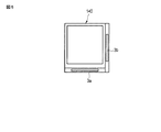
図2に図1のA−A’断面図、図3に図1のB−B’断面図を各々示す。 2 is a cross-sectional view taken along line A-A ′ of FIG. 1, and FIG. 3 is a cross-sectional view taken along line B-B ′ of FIG. 1.
図示するように、液晶表示素子110は、アレイ基板31と対向基板32を有する。アレイ基板31は、第1の基板11、第1の基板11の一主面上に形成された下地樹脂層13、及び下地樹脂層13上にマトリクス状に形成されて表示領域101を構成する複数の画素電極14を含む。
As illustrated, the liquid
一方、対向基板32は、アレイ基板31に対向して設けられ、第2の基板12、第2の基板12の表示領域101に形成された着色層16、及び周辺領域102に形成され、周辺領域102を遮蔽する遮光層2、及び共通電極17を含む。
On the other hand, the
シール材19は、アレイ基板31と対向基板32とを表示領域101周囲の周辺領域102において接着する。
The sealing
複数のスペーサー15aは下地樹脂層2上の周辺領域102に形成され、シール材19中に設けられている。
The plurality of
アレイ基板31と対向基板32とシール材19とにより区画された領域には液晶18が封入されている。
A
また、下地樹脂層2上の表示領域101にはスペーサー15cを形成することができる。スペーサー15cは液晶18中に設けられている。
In addition, a
液晶表示素子110と隣接する液晶表示素子120との間には、マザー基板から切り離された後の工程で液晶表示素子にIC3が設けられるので、このA-A’断面では、液晶表示素子110と隣接する液晶表示素子120との距離が離れている。
Since the liquid crystal display element IC3 is provided between the liquid
一方、図示するように、B-B’断面では、液晶表示素子110と隣接する液晶表示素子130との間にはIC3を配置しないため、液晶表示素子110と隣接する液晶表示素子130との距離が近接している。
On the other hand, as shown in the drawing, since the IC 3 is not disposed between the liquid
複数のスペーサー15bは下地樹脂層2上の周辺領域102に形成され、シール材19中に設けられている。
The plurality of
図示するように、実施形態によれば、実装辺に設けられたスペーサー15aを対向基板側から見た場合の面密度は、実装辺とは異なる辺に設けられたスペーサー15bの面密度よりも高い。
As illustrated, according to the embodiment, the surface density when the
シール材中のスペーサーは、その上部にはシール材が載り上げ、シール材が他方の基板に接するような構造となる。このスペーサー上部に載ったシール材の厚みをここでは「噛み込み量」と記述する。 The spacer in the sealing material has a structure in which the sealing material is placed on the spacer and the sealing material is in contact with the other substrate. Here, the thickness of the sealing material placed on the upper portion of the spacer is described as “biting amount”.
尚、アレイ基板31と対向基板32の外側には、図示しない偏光板、位相差板等の光学素子が配置される。
Note that optical elements such as a polarizing plate and a retardation plate (not shown) are disposed outside the array substrate 31 and the
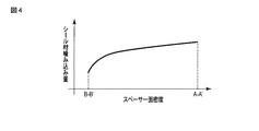
図4にスペーサー密度と、噛み込み量との関係を表すグラフを示す。 FIG. 4 is a graph showing the relationship between the spacer density and the amount of biting.
この接着剤の噛み込み量は、図3に示すように、スペーサー密度が高い程、大きくなる。これを利用して、スペーサーの高さが表示領域に対して周辺領域が低く、特に実装辺のスペーサーの高さが低いことから生ずる重力ムラに対し、周辺領域に配置するスペーサー密度を調整することで解決する。即ち、実装辺の周辺領域のスペーサーの高さが最も低いことから、この領域のスペーサー密度を、実装辺以外の辺より高く設定することで、重力ムラを抑制することができる。 As shown in FIG. 3, the amount of this adhesive biting increases as the spacer density increases. Use this to adjust the density of spacers arranged in the peripheral area against the unevenness of gravity caused by the spacer being lower in the peripheral area than the display area, and in particular the low height of the spacer on the mounting side. To solve. That is, since the height of the spacer in the peripheral region of the mounting side is the lowest, unevenness in gravity can be suppressed by setting the spacer density in this region higher than the side other than the mounting side.
図5に、実施形態にかかる液晶表示素子の他の一例を表す図を示す。 FIG. 5 is a diagram illustrating another example of the liquid crystal display element according to the embodiment.
なお、図1ないし図3の液晶表示素子110,120,130では、各々、1つの実装辺にICが設けられているが、図5に示すように、1つの液晶表示層140が2つの実装辺に各々1つずつのICが設けられていても良い。
In each of the liquid
実施例
以下のように、図1及び図2に示す構成と同様の構成を有する液晶表示素子を形成した。
Example A liquid crystal display device having the same configuration as that shown in FIGS. 1 and 2 was formed as follows.
ガラス基板11上に、スリットコータを用いて下地樹脂層13を形成した。
A
下地樹脂層13上に、マトリクス状の画素電極14を形成した。
A matrix-
表示領域101及び周辺領域102の下地樹脂層13上にスペーサー材料塗布層を形成し、パターニングを行うことによりスペーサーを形成し、アレイ基板31を得た。
A spacer material coating layer was formed on the
さらに、ガラス基板12上の表示領域に着色層、周辺領域に遮蔽層を形成した。さらに絶縁層を介して共通電極17を形成し、対向基板32を得た。
Further, a colored layer was formed in the display area on the
アレイ基板31と対向基板32の周辺領域をシール材19で接着した。
The peripheral region of the array substrate 31 and the
尚、滴下注入方式によりアレイ基板31と対向基板32とシール材19とで区画された領域に、液晶18を封入した。
The
その後、所定の位置にIC3を設けて、液晶表示素子を得た。 Then, IC3 was provided in the predetermined position and the liquid crystal display element was obtained.
シール材中のスペーサー15a,15b、表示領域のスペーサー15cと同時に形成した。アレイ基板側の下地樹脂層13のパターン端部はシール材の一部まで延出させた。スペーサー15a,15bはその下地樹脂層13のパターン端部に形成される。スペーサーを形成するための樹脂塗布層はレベリングにより下地樹脂層13の中央よりも端部の方が厚さが減少するので、表示領域のスペーサー15cに比べてスペーサー15a,15bの高さが低くなる。
The
また、実装辺側のスペーサー15aは隣接する他2辺のスペーサー15bに比べ下地樹脂層13のパターン抜き量が大きい。すなわち図3の領域202に比べ図2の領域201の方が大きくスペーサーを形成するための樹脂膜のレベリングにより、実装辺側の下地樹脂層13端部でのスペーサーを形成するための樹脂塗布層の厚さは、実装辺以外の他辺の下地樹脂層13端部での樹脂塗布層の厚さより薄くなる。このため、パターニング後の実装辺側のスペーサー15aの高さは実装辺以外の他辺側のスペーサー15bに比べより低くなる。
The
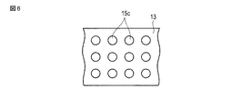
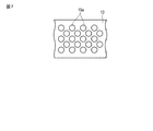
このため、実施例では、シール材のスペーサー面密度を、実装辺部が隣接する他2辺に比べて高く設定する。ここで、ICに隣接する実装辺に設けられたスペーサー15aを対向基板側から見た場合の面密度を表す図を図6に、実装辺とは異なる辺に設けられたスペーサー15bの面密度を表す図を図7に示す。
For this reason, in an Example, the spacer surface density of a sealing material is set high compared with the other 2 sides where a mounting side part adjoins. Here, FIG. 6 is a diagram showing the surface density when the
ここでは、スペーサー15aの配列は、スペーサー15bの配列の間にさらにスペーサーを設け、千鳥格子状の配列にすることにより、面密度をさらに高くしている。
Here, the arrangement of the
これにより、シール材の噛み込み量が多くなり、シール材の高さや辺に依らず画像品質を均一に保つことができる。 As a result, the amount of the sealing material is increased, and the image quality can be kept uniform regardless of the height and sides of the sealing material.
さらに、滴下注入において、実装辺のシール材が潰れることなく、隣接する他2辺同様に高さが保持され、重力ムラの発生が抑制できる。 Further, in dropping injection, the sealing material on the mounting side is not crushed, and the height is maintained in the same manner as the other two adjacent sides, thereby suppressing the occurrence of gravity unevenness.
比較例
比較として、周辺領域のスペーサー面密度を、実装辺とが隣接する他2辺と同じ設定にした。接着剤の噛み込み量は同じとなる。結果、周辺領域の高さは、周辺領域のスペーサーの高さが反映され、実装辺のみ低くなる。
Comparative Example For comparison, the spacer surface density in the peripheral region was set to the same setting as the other two sides adjacent to the mounting side. The amount of adhesive biting is the same. As a result, the height of the peripheral region reflects the height of the spacer in the peripheral region, and only the mounting side is lowered.
その結果、滴下注入において実装辺の周辺領域がつぶれて、重力ムラが発生した。 As a result, the peripheral area of the mounting side was crushed during the drop injection, and gravity unevenness occurred.
以上のように、実施形態によれば、実装辺の接着剤領域のスペーサー面密度を、接する二辺に対し高く設定することで、接着剤の噛み込み量が多くなり、接する二辺同等のセルギャップを実現することができる。これにより、表示領域に対して、周辺部のセルギャップが適切に保持される。特に実装辺近傍のセルギャップが低すぎる不具合を解消することで、重力ムラ発生を抑制することができる。 As described above, according to the embodiment, by setting the spacer area density of the adhesive region on the mounting side to be higher than the two sides in contact with each other, the amount of the adhesive is increased, and the cells equivalent to the two sides in contact are obtained. A gap can be realized. Thereby, the cell gap in the peripheral portion is appropriately maintained with respect to the display area. In particular, by eliminating the problem that the cell gap in the vicinity of the mounting side is too low, the occurrence of gravity unevenness can be suppressed.
実施例においては、滴下注入方式の場合のみを述べたが、他の貼り合わせ方法においても、本実施形態は有効である。 In the examples, only the case of the dropping injection method has been described, but the present embodiment is also effective in other bonding methods.
また、実施例としてアレイ基板側にスペーサーを配置する構成のみを述べたが、対向基板側にスペーサーを配置する構成においても、本実施形態は有効である。 Further, only the configuration in which the spacer is arranged on the array substrate side has been described as an example, but the present embodiment is also effective in the configuration in which the spacer is arranged on the counter substrate side.
本発明のいくつかの実施形態を説明したが、これらの実施形態は、例として提示したものであり、発明の範囲を限定することは意図していない。これら新規な実施形態は、その他の様々な形態で実施されることが可能であり、発明の要旨を逸脱しない範囲で、種々の省略、置き換え、変更を行うことができる。これら実施形態やその変形は、発明の範囲や要旨に含まれるとともに、特許請求の範囲に記載された発明とその均等の範囲に含まれる。 Although several embodiments of the present invention have been described, these embodiments are presented by way of example and are not intended to limit the scope of the invention. These novel embodiments can be implemented in various other forms, and various omissions, replacements, and changes can be made without departing from the scope of the invention. These embodiments and modifications thereof are included in the scope and gist of the invention, and are included in the invention described in the claims and the equivalents thereof.
11…第1の基板、12…第2の基板、13…下地樹脂層、14…画素電極、15a,15b,15c…スペーサー、16…着色層、17…共通電極、18…液晶、19…シール材、31…アレイ基板、32…対向基板、110,120,130…液晶表示素子
DESCRIPTION OF
Claims (2)
該アレイ基板に対向して設けられ、第2の基板、及び該第2の基板上に形成され、該表示領域周囲の周辺領域を遮蔽する遮光層を含む対向基板と、
該アレイ基板と該対向基板とを該周辺領域において接着するシール材と、
該下地樹脂層上の該周辺領域に形成され、該シール材中に設けられた複数のスペーサーと、
該アレイ基板と該対向基板とシール材とにより区画された領域に封入された液晶とを具備する液晶表示装置であって、
前記シール材において、前記ICに隣接する実装辺に設けられたスペーサーを対向基板側から見た場合の面密度は、その他の辺に設けられたスペーサーの面密度に比べて高いことを特徴とする液晶表示装置。 A first substrate; a base resin layer formed on one main surface of the first substrate; a plurality of pixel electrodes formed in a matrix on the base resin layer to form a display region; and the first substrate An array substrate including an IC mounted on one main surface of the substrate with a space from the base resin layer;
A counter substrate provided opposite to the array substrate, including a second substrate, and a light shielding layer formed on the second substrate and shielding a peripheral region around the display region;
A sealing material for bonding the array substrate and the counter substrate in the peripheral region;
A plurality of spacers formed in the peripheral region on the base resin layer and provided in the sealing material;
A liquid crystal display device comprising a liquid crystal sealed in a region defined by the array substrate, the counter substrate, and a sealing material,
In the sealing material, the surface density when the spacer provided on the mounting side adjacent to the IC is viewed from the counter substrate side is higher than the surface density of the spacer provided on the other side. Liquid crystal display device.
Priority Applications (2)
| Application Number | Priority Date | Filing Date | Title |
|---|---|---|---|
| JP2012184023A JP2014041282A (en) | 2012-08-23 | 2012-08-23 | Liquid crystal display device |
| US13/960,137 US9442326B2 (en) | 2012-08-23 | 2013-08-06 | Liquid crystal display device |
Applications Claiming Priority (1)
| Application Number | Priority Date | Filing Date | Title |
|---|---|---|---|
| JP2012184023A JP2014041282A (en) | 2012-08-23 | 2012-08-23 | Liquid crystal display device |
Publications (2)
| Publication Number | Publication Date |
|---|---|
| JP2014041282A true JP2014041282A (en) | 2014-03-06 |
| JP2014041282A5 JP2014041282A5 (en) | 2015-10-08 |
Family
ID=50147720
Family Applications (1)
| Application Number | Title | Priority Date | Filing Date |
|---|---|---|---|
| JP2012184023A Pending JP2014041282A (en) | 2012-08-23 | 2012-08-23 | Liquid crystal display device |
Country Status (2)
| Country | Link |
|---|---|
| US (1) | US9442326B2 (en) |
| JP (1) | JP2014041282A (en) |
Cited By (2)
| Publication number | Priority date | Publication date | Assignee | Title |
|---|---|---|---|---|
| US9274380B2 (en) | 2013-06-06 | 2016-03-01 | Japan Display Inc. | Liquid crystal display device comprising a mounting portion located in a circumference area for mounting a signal source and method of manufacturing the same |
| KR20200026299A (en) | 2017-08-23 | 2020-03-10 | 데쿠세리아루즈 가부시키가이샤 | Spacer containing tape |
Families Citing this family (13)
| Publication number | Priority date | Publication date | Assignee | Title |
|---|---|---|---|---|
| JP6205113B2 (en) | 2012-08-24 | 2017-09-27 | 株式会社ジャパンディスプレイ | Liquid crystal display |
| CN103995385B (en) * | 2014-05-09 | 2017-12-05 | 京东方科技集团股份有限公司 | Display master blank and its cutting method |
| CN104678658B (en) * | 2015-02-13 | 2018-04-20 | 深超光电(深圳)有限公司 | Display panel and preparation method thereof |
| CN104793404B (en) * | 2015-04-24 | 2018-09-11 | 合肥京东方光电科技有限公司 | A kind of display panel and its liquid crystal display device |
| CN104865754A (en) * | 2015-06-19 | 2015-08-26 | 合肥鑫晟光电科技有限公司 | Display panel and manufacturing method thereof as well as display device |
| CN108572478A (en) * | 2017-03-13 | 2018-09-25 | 南京瀚宇彩欣科技有限责任公司 | Display |
| CN108490676A (en) * | 2018-03-23 | 2018-09-04 | 惠州市华星光电技术有限公司 | Liquid crystal display and its manufacturing method |
| CN108828820A (en) * | 2018-06-27 | 2018-11-16 | 豪威半导体(上海)有限责任公司 | LCoS display panel and its manufacturing method |
| CN108919545B (en) * | 2018-06-28 | 2021-05-04 | 厦门天马微电子有限公司 | Display panel and display device |
| CN109243305B (en) * | 2018-09-17 | 2021-10-12 | 京东方科技集团股份有限公司 | Display panel, display device, and method for manufacturing display panel |
| CN109061934B (en) * | 2018-09-30 | 2021-04-30 | 厦门天马微电子有限公司 | Display panel and display device |
| CN111427198A (en) * | 2020-05-12 | 2020-07-17 | 合肥鑫晟光电科技有限公司 | Display substrate, preparation method thereof and display device |
| CN111968517B (en) * | 2020-08-31 | 2022-11-01 | 合肥维信诺科技有限公司 | Display panel and display device |
Citations (5)
| Publication number | Priority date | Publication date | Assignee | Title |
|---|---|---|---|---|
| JP2003121860A (en) * | 2001-10-17 | 2003-04-23 | Matsushita Electric Ind Co Ltd | Liquid crystal display panel |
| JP2007193153A (en) * | 2006-01-20 | 2007-08-02 | Epson Imaging Devices Corp | Electrooptical apparatus, method for manufacturing electrooptical apparatus, and electronic apparatus |
| WO2007119409A1 (en) * | 2006-03-31 | 2007-10-25 | Citizen Holdings Co., Ltd. | Large-sized substrate and liquid crystal device employing the large-sized substrate and method for producing the liquid crystal device |
| JP2012058423A (en) * | 2010-09-08 | 2012-03-22 | Hitachi Displays Ltd | Liquid crystal display device |
| WO2012060302A1 (en) * | 2010-11-02 | 2012-05-10 | シャープ株式会社 | Liquid crystal display device |
Family Cites Families (17)
| Publication number | Priority date | Publication date | Assignee | Title |
|---|---|---|---|---|
| JPH09120062A (en) * | 1995-08-18 | 1997-05-06 | Toshiba Electron Eng Corp | Color filter substrate and its production and liquid crystal display element formed by using the same and its production |
| US6888608B2 (en) * | 1995-09-06 | 2005-05-03 | Kabushiki Kaisha Toshiba | Liquid crystal display device |
| JPH10153785A (en) * | 1996-09-26 | 1998-06-09 | Toshiba Corp | Liquid crystal display device |
| JP2003279998A (en) | 2002-03-22 | 2003-10-02 | Hitachi Ltd | Liquid crystal display device |
| JP4156445B2 (en) * | 2003-06-04 | 2008-09-24 | 株式会社 日立ディスプレイズ | Manufacturing method of liquid crystal display device |
| JP2005338770A (en) * | 2004-04-26 | 2005-12-08 | Nec Lcd Technologies Ltd | Liquid crystal display device |
| TWI343492B (en) * | 2005-02-01 | 2011-06-11 | Samsung Electronics Co Ltd | Liquid crystal display and method of fabricating the same |
| JP4723283B2 (en) * | 2005-05-19 | 2011-07-13 | シチズンホールディングス株式会社 | Manufacturing method of liquid crystal panel |
| JP2007114704A (en) * | 2005-10-24 | 2007-05-10 | Nec Lcd Technologies Ltd | Liquid crystal display apparatus and method for manufacturing the same |
| JP4795127B2 (en) * | 2006-06-06 | 2011-10-19 | 三菱電機株式会社 | Liquid crystal display device and manufacturing method thereof |
| TWI288846B (en) * | 2006-06-16 | 2007-10-21 | Innolux Display Corp | Liquid crystal display |
| TW200823573A (en) * | 2006-11-17 | 2008-06-01 | Au Optronics Corp | Liquid crystal display panel and manufacture method thereof |
| TWI345652B (en) * | 2006-12-01 | 2011-07-21 | Chimei Innolux Corp | Liquid crystal panel and method of manufacturing the same |
| JP2010231193A (en) * | 2009-03-03 | 2010-10-14 | Toshiba Mobile Display Co Ltd | Liquid crystal display |
| KR101701977B1 (en) * | 2010-08-09 | 2017-02-03 | 삼성디스플레이 주식회사 | Liquid crystal display device |
| US8976094B2 (en) * | 2011-05-05 | 2015-03-10 | Apple Inc. | Display edge seal improvement |
| JP5972041B2 (en) * | 2012-05-15 | 2016-08-17 | 三菱電機株式会社 | Liquid crystal display |
-
2012
- 2012-08-23 JP JP2012184023A patent/JP2014041282A/en active Pending
-
2013
- 2013-08-06 US US13/960,137 patent/US9442326B2/en active Active
Patent Citations (5)
| Publication number | Priority date | Publication date | Assignee | Title |
|---|---|---|---|---|
| JP2003121860A (en) * | 2001-10-17 | 2003-04-23 | Matsushita Electric Ind Co Ltd | Liquid crystal display panel |
| JP2007193153A (en) * | 2006-01-20 | 2007-08-02 | Epson Imaging Devices Corp | Electrooptical apparatus, method for manufacturing electrooptical apparatus, and electronic apparatus |
| WO2007119409A1 (en) * | 2006-03-31 | 2007-10-25 | Citizen Holdings Co., Ltd. | Large-sized substrate and liquid crystal device employing the large-sized substrate and method for producing the liquid crystal device |
| JP2012058423A (en) * | 2010-09-08 | 2012-03-22 | Hitachi Displays Ltd | Liquid crystal display device |
| WO2012060302A1 (en) * | 2010-11-02 | 2012-05-10 | シャープ株式会社 | Liquid crystal display device |
Cited By (13)
| Publication number | Priority date | Publication date | Assignee | Title |
|---|---|---|---|---|
| US11086169B2 (en) | 2013-06-06 | 2021-08-10 | Japan Display Inc. | Display device comprising a resin layer having a first width larger than a second width and an end surface of a seal material and an air gap overlap the resin layer |
| US9405155B2 (en) | 2013-06-06 | 2016-08-02 | Japan Display Inc. | Liquid crystal display device comprising a mounting portion located in a circumference area for mounting a signal source and method of manufacturing the same |
| US9823523B2 (en) | 2013-06-06 | 2017-11-21 | Japan Display Inc. | Display device comprising a mounting portion located in a circumference area for mounting a signal source |
| US10359670B2 (en) | 2013-06-06 | 2019-07-23 | Japan Display Inc. | Display device comprising first and second insulating films having respective first and second concave portions facing each other |
| US10670925B2 (en) | 2013-06-06 | 2020-06-02 | Japan Display Inc. | Display device comprising a first insulating layer having a first concave portion formed between a resin layer and a pillar-shaped spacer |
| US9274380B2 (en) | 2013-06-06 | 2016-03-01 | Japan Display Inc. | Liquid crystal display device comprising a mounting portion located in a circumference area for mounting a signal source and method of manufacturing the same |
| US11372277B2 (en) | 2013-06-06 | 2022-06-28 | Japan Display Inc. | Display device comprising first and second polarizing plates having ends located inside an end of a second substrate and an air gap between a resin layer and a second organic insulating film |
| US11614648B2 (en) | 2013-06-06 | 2023-03-28 | Japan Display Inc. | Display device comprising first and second polarizing plates having ends located inside an end of a second substrate and an air gap between a resin layer and an organic insulating film |
| US11841567B2 (en) | 2013-06-06 | 2023-12-12 | Japan Display Inc. | Display device comprising first and second polarizing plates having ends located inside an end of a second substrate and an air gap between a resin layer and the second substrate |
| KR20200026299A (en) | 2017-08-23 | 2020-03-10 | 데쿠세리아루즈 가부시키가이샤 | Spacer containing tape |
| KR20210122875A (en) | 2017-08-23 | 2021-10-12 | 데쿠세리아루즈 가부시키가이샤 | Spacer-containing tape |
| US11327368B2 (en) | 2017-08-23 | 2022-05-10 | Dexerials Corporation | Spacer-containing tape |
| US11796865B2 (en) | 2017-08-23 | 2023-10-24 | Dexerials Corporation | Spacer-containing tape |
Also Published As
| Publication number | Publication date |
|---|---|
| US9442326B2 (en) | 2016-09-13 |
| US20140055735A1 (en) | 2014-02-27 |
Similar Documents
| Publication | Publication Date | Title |
|---|---|---|
| JP2014041282A (en) | Liquid crystal display device | |
| US8994909B2 (en) | Liquid crystal display panel and liquid crystal display device | |
| US9897861B2 (en) | Liquid crystal display device and liquid crystal display panel thereof | |
| KR101647882B1 (en) | Display device and method of manufacturing the same | |
| JP4376266B2 (en) | Color filter substrate and liquid crystal display panel including the same | |
| TWI454809B (en) | Liquid crystal display panel | |
| US9523888B2 (en) | Liquid crystal display substrate, liquid crystal display panel and liquid crystal display device | |
| US20050190335A1 (en) | Liquid crystal display device having an injection hole for liquid crystal | |
| US7688416B2 (en) | Liquid crystal display device | |
| US11243441B2 (en) | Display panel, display apparatus, method of fabricating display panel, and operating method of operating display panel | |
| JP7248591B2 (en) | Color filter substrate and its manufacturing method, display panel and display device | |
| WO2018196438A1 (en) | Display panel and manufacturing method therefor, and display device | |
| JP6223809B2 (en) | Display device | |
| US7911576B2 (en) | Manufacturing method of liquid crystal display device | |
| JP2006071750A (en) | Liquid crystal display | |
| US10031376B2 (en) | Liquid crystal display device | |
| US20050264750A1 (en) | Liquid crystal display apparatus with highly uniform substrate gap | |
| JP2009168832A (en) | Liquid crystal display and method of manufacturing the same | |
| JP5143664B2 (en) | LCD panel | |
| JP5128305B2 (en) | Liquid crystal display | |
| US9128330B2 (en) | Liquid crystal display device and method of manufacturing the same | |
| US20130010250A1 (en) | Liquid crystal display device and manufacturing method thereof | |
| KR101654239B1 (en) | Liquid crystal display device and method of fabricating the same | |
| KR20130025219A (en) | Liquid crystal display | |
| JP5555649B2 (en) | LCD panel |
Legal Events
| Date | Code | Title | Description |
|---|---|---|---|
| A521 | Written amendment |
Free format text: JAPANESE INTERMEDIATE CODE: A523 Effective date: 20150819 |
|
| A621 | Written request for application examination |
Free format text: JAPANESE INTERMEDIATE CODE: A621 Effective date: 20150819 |
|
| A131 | Notification of reasons for refusal |
Free format text: JAPANESE INTERMEDIATE CODE: A131 Effective date: 20160419 |
|
| A977 | Report on retrieval |
Free format text: JAPANESE INTERMEDIATE CODE: A971007 Effective date: 20160420 |
|
| A02 | Decision of refusal |
Free format text: JAPANESE INTERMEDIATE CODE: A02 Effective date: 20161018 |