JP2014029428A - Signal processing circuit, display device, electrical apparatus, and signal processing method - Google Patents
Signal processing circuit, display device, electrical apparatus, and signal processing method Download PDFInfo
- Publication number
- JP2014029428A JP2014029428A JP2012170369A JP2012170369A JP2014029428A JP 2014029428 A JP2014029428 A JP 2014029428A JP 2012170369 A JP2012170369 A JP 2012170369A JP 2012170369 A JP2012170369 A JP 2012170369A JP 2014029428 A JP2014029428 A JP 2014029428A
- Authority
- JP
- Japan
- Prior art keywords
- video signal
- correction
- signal
- signal processing
- video
- Prior art date
- Legal status (The legal status is an assumption and is not a legal conclusion. Google has not performed a legal analysis and makes no representation as to the accuracy of the status listed.)
- Pending
Links
Images


Classifications
-
- G—PHYSICS
- G09—EDUCATION; CRYPTOGRAPHY; DISPLAY; ADVERTISING; SEALS
- G09G—ARRANGEMENTS OR CIRCUITS FOR CONTROL OF INDICATING DEVICES USING STATIC MEANS TO PRESENT VARIABLE INFORMATION
- G09G3/00—Control arrangements or circuits, of interest only in connection with visual indicators other than cathode-ray tubes
- G09G3/20—Control arrangements or circuits, of interest only in connection with visual indicators other than cathode-ray tubes for presentation of an assembly of a number of characters, e.g. a page, by composing the assembly by combination of individual elements arranged in a matrix no fixed position being assigned to or needed to be assigned to the individual characters or partial characters
- G09G3/22—Control arrangements or circuits, of interest only in connection with visual indicators other than cathode-ray tubes for presentation of an assembly of a number of characters, e.g. a page, by composing the assembly by combination of individual elements arranged in a matrix no fixed position being assigned to or needed to be assigned to the individual characters or partial characters using controlled light sources
- G09G3/30—Control arrangements or circuits, of interest only in connection with visual indicators other than cathode-ray tubes for presentation of an assembly of a number of characters, e.g. a page, by composing the assembly by combination of individual elements arranged in a matrix no fixed position being assigned to or needed to be assigned to the individual characters or partial characters using controlled light sources using electroluminescent panels
-
- G—PHYSICS
- G09—EDUCATION; CRYPTOGRAPHY; DISPLAY; ADVERTISING; SEALS
- G09G—ARRANGEMENTS OR CIRCUITS FOR CONTROL OF INDICATING DEVICES USING STATIC MEANS TO PRESENT VARIABLE INFORMATION
- G09G3/00—Control arrangements or circuits, of interest only in connection with visual indicators other than cathode-ray tubes
- G09G3/20—Control arrangements or circuits, of interest only in connection with visual indicators other than cathode-ray tubes for presentation of an assembly of a number of characters, e.g. a page, by composing the assembly by combination of individual elements arranged in a matrix no fixed position being assigned to or needed to be assigned to the individual characters or partial characters
- G09G3/2007—Display of intermediate tones
- G09G3/2044—Display of intermediate tones using dithering
- G09G3/2051—Display of intermediate tones using dithering with use of a spatial dither pattern
-
- G—PHYSICS
- G09—EDUCATION; CRYPTOGRAPHY; DISPLAY; ADVERTISING; SEALS
- G09G—ARRANGEMENTS OR CIRCUITS FOR CONTROL OF INDICATING DEVICES USING STATIC MEANS TO PRESENT VARIABLE INFORMATION
- G09G2310/00—Command of the display device
- G09G2310/02—Addressing, scanning or driving the display screen or processing steps related thereto
- G09G2310/0264—Details of driving circuits
- G09G2310/027—Details of drivers for data electrodes, the drivers handling digital grey scale data, e.g. use of D/A converters
-
- G—PHYSICS
- G09—EDUCATION; CRYPTOGRAPHY; DISPLAY; ADVERTISING; SEALS
- G09G—ARRANGEMENTS OR CIRCUITS FOR CONTROL OF INDICATING DEVICES USING STATIC MEANS TO PRESENT VARIABLE INFORMATION
- G09G2320/00—Control of display operating conditions
- G09G2320/02—Improving the quality of display appearance
- G09G2320/0271—Adjustment of the gradation levels within the range of the gradation scale, e.g. by redistribution or clipping
-
- G—PHYSICS
- G09—EDUCATION; CRYPTOGRAPHY; DISPLAY; ADVERTISING; SEALS
- G09G—ARRANGEMENTS OR CIRCUITS FOR CONTROL OF INDICATING DEVICES USING STATIC MEANS TO PRESENT VARIABLE INFORMATION
- G09G2320/00—Control of display operating conditions
- G09G2320/02—Improving the quality of display appearance
- G09G2320/0285—Improving the quality of display appearance using tables for spatial correction of display data
-
- G—PHYSICS
- G09—EDUCATION; CRYPTOGRAPHY; DISPLAY; ADVERTISING; SEALS
- G09G—ARRANGEMENTS OR CIRCUITS FOR CONTROL OF INDICATING DEVICES USING STATIC MEANS TO PRESENT VARIABLE INFORMATION
- G09G2320/00—Control of display operating conditions
- G09G2320/06—Adjustment of display parameters
- G09G2320/0673—Adjustment of display parameters for control of gamma adjustment, e.g. selecting another gamma curve
Abstract
Description
本技術は、映像信号に対して補正を行う信号処理回路ならびにそれを備えた表示装置および電子機器に関する。また、本技術は、映像信号に対して補正を行う信号処理方法に関する。 The present technology relates to a signal processing circuit that corrects a video signal, a display device including the signal processing circuit, and an electronic apparatus. The present technology also relates to a signal processing method for correcting a video signal.
近年、映像表示を行う表示装置の分野では、画素の発光素子として、流れる電流値に応じて発光輝度が変化する電流駆動型の発光素子、例えば有機EL素子を用いた表示装置が開発され、商品化が進められている。有機EL素子は、液晶素子などと異なり自発光素子である。そのため、有機EL素子を用いた表示装置(有機EL表示装置)では、光源(バックライト)が必要ないので、光源を必要とする液晶表示装置と比べて、薄型化、高輝度化することができる。 In recent years, in the field of display devices that perform video display, display devices using current-driven light-emitting elements, for example, organic EL elements, whose light emission luminance changes according to the value of a flowing current have been developed as light-emitting elements of pixels. Is being promoted. Unlike a liquid crystal element or the like, the organic EL element is a self-luminous element. Therefore, a display device (organic EL display device) using an organic EL element does not require a light source (backlight), so that it can be made thinner and brighter than a liquid crystal display device that requires a light source. .
有機EL表示装置では、製造時のTFT特性のばらつきによって、表示映像に、スジや、輝度ムラが生じることがある。通常、このような表示不良を防ぐために、画素回路に含まれるTFT(Thin Film Transistor)の駆動方法により自己補正を行う手法(Vth補正)が一般的に行われている。しかし、実際には、それだけでは不十分な場合もあり、その場合には、Vth補正の他に、TFTのゲート−ソース間に保持される電圧をTFTの移動度μの大きさに応じて補正するμ補正が行われることがある(例えば、特許文献1参照)。 In an organic EL display device, streaks and luminance unevenness may occur in a display image due to variations in TFT characteristics during manufacturing. In general, in order to prevent such a display defect, a method (Vth correction) in which self-correction is performed by a driving method of a TFT (Thin Film Transistor) included in a pixel circuit is generally performed. In practice, however, that alone may not be sufficient. In this case, in addition to Vth correction, the voltage held between the gate and the source of the TFT is corrected according to the magnitude of the TFT mobility μ. Μ correction may be performed (see, for example, Patent Document 1).
μ補正では、表示時に使用する電圧よりも高い電圧が使用される。そのため、μ補正を行う場合には、μ補正を行わない場合よりも、高耐圧のドライバICが必要となり、さらに、ドライバICから発せられる発熱量が大きくなる。従って、駆動系システムを小型化し、さらに、低消費電力化する必要のあるモバイル系機器では、μ補正を行わずに表示不良を防止する方策が必要となる。 In the μ correction, a voltage higher than the voltage used at the time of display is used. Therefore, when μ correction is performed, a driver IC with a high breakdown voltage is required, and the amount of heat generated from the driver IC is larger than when μ correction is not performed. Therefore, a mobile device that needs to reduce the size of the drive system and further reduce the power consumption requires a measure for preventing display defects without performing μ correction.
そのような方策として、例えば、特許文献2〜5に記載の方策が提案されている。特許文献2では、レーザアニール時に基板を回転させ、エネルギー密度のばらつきを平準化することが開示されている。しかし、この方策では、製造時間の増大によって、製造コストが上昇してしまうという問題があった。また、特許文献3〜5では、個々の表示パネルの発光特性を測定し、その測定データに基づいて作成した補正データで映像信号を補正することにより表示不良を防止することが開示されている。しかし、この方策では、表示パネルごとに発光特性を測定することが必要となる。そのため、この方策でも、製造時間の増大によって、製造コストが上昇してしまうという問題があった。 As such measures, for example, measures described in Patent Documents 2 to 5 have been proposed. Patent Document 2 discloses that a substrate is rotated at the time of laser annealing to level out variations in energy density. However, this measure has a problem that the manufacturing cost increases due to an increase in manufacturing time. Patent Documents 3 to 5 disclose that display defects are prevented by measuring light emission characteristics of individual display panels and correcting video signals with correction data created based on the measurement data. However, with this measure, it is necessary to measure the light emission characteristics for each display panel. Therefore, even with this measure, there is a problem that the manufacturing cost increases due to an increase in manufacturing time.
なお、表示映像に、スジや、輝度ムラが生じる問題は、有機EL表示装置に特有の問題ではない。例えば、複数のμmオーダーのLED(Light Emitting Diode)が表示画素としてマトリクス状に配置されたLEDディスプレイにおいても、LED特性のばらつきによって、表示映像に、スジや、輝度ムラが生じることがある。 Note that the problem of streaks and uneven brightness in the display image is not a problem specific to the organic EL display device. For example, even in an LED display in which a plurality of LEDs (light emitting diodes) on the order of μm are arranged in a matrix as display pixels, streaks and uneven brightness may occur in a display image due to variations in LED characteristics.
本技術はかかる問題点に鑑みてなされたもので、その第1の目的は、製造時間を増大させることなく表示不良を防止することの可能な信号処理回路ならびにそれを備えた表示装置および電子機器を提供することにある。また、第2の目的は、製造時間を増大させることなく表示不良を防止する信号処理方法を提供することにある。 The present technology has been made in view of such problems, and a first object thereof is a signal processing circuit capable of preventing display defects without increasing manufacturing time, and a display device and an electronic apparatus including the signal processing circuit. Is to provide. A second object is to provide a signal processing method for preventing display defects without increasing the manufacturing time.
本技術の信号処理回路は、規則性を有するノイズ状の模様が映像に生成されるように第1の映像信号に対して補正を行うことにより第2の映像信号を生成するものである。 The signal processing circuit of the present technology generates a second video signal by correcting the first video signal so that a noise-like pattern having regularity is generated in the video.
本技術の表示装置は、表示パネルと、表示パネルを駆動する駆動回路とを備えている。駆動回路は、上記の信号処理回路を有している。 The display device of the present technology includes a display panel and a drive circuit that drives the display panel. The drive circuit has the signal processing circuit described above.
本技術の電子機器は、上記の表示装置を備えている。 An electronic apparatus of the present technology includes the display device described above.
本技術の信号処理方法は、規則性を有するノイズ状の模様が映像に生成されるように第1の映像信号に対して補正を行うことにより第2の映像信号を生成するステップを含むものである。 The signal processing method of the present technology includes a step of generating a second video signal by correcting the first video signal so that a noise-like pattern having regularity is generated in the video.
本技術の信号処理回路、表示装置、電子機器、および信号処理方法では、規則性を有するノイズ状の模様が映像に生成されるように第1の映像信号に対して補正を行うことにより第2の映像信号が生成される。これにより、表示パネルに第1の映像信号が入力された場合の表示映像に、スジや輝度ムラが生じる場合であっても、その表示映像に、それらを目立たなくさせる模様を重畳させることができる。また、本技術では、表示映像に重畳される模様が、規則性を有するノイズ状の模様であり、表示パネルの発光特性を測定することなく得られる模様である。従って、表示映像に上記の模様を重畳するために、表示パネルの発光特性を測定する必要がない。 In the signal processing circuit, the display device, the electronic device, and the signal processing method of the present technology, the second video signal is corrected by correcting the first video signal so that a regular noise pattern is generated in the video. Video signals are generated. As a result, even when streaks or luminance unevenness occurs in the display video when the first video signal is input to the display panel, a pattern that makes them inconspicuous can be superimposed on the display video. . In the present technology, the pattern superimposed on the display image is a noise-like pattern having regularity, and is a pattern obtained without measuring the light emission characteristics of the display panel. Therefore, it is not necessary to measure the light emission characteristics of the display panel in order to superimpose the above pattern on the display image.
本技術の信号処理回路、表示装置、電子機器、および信号処理方法によれば、表示パネルに第1の映像信号が入力された場合の表示映像に、スジや輝度ムラが生じる場合であっても、その表示映像に、それらを目立たなくさせる模様を重畳させることができるようにしたので、スジや輝度ムラなどの表示不良を防止することができる。また、表示映像に上記の模様を重畳するために、表示パネルの発光特性を測定する必要がないので、製造時間を増大させる虞がない。以上のことから、本技術では、製造時間を増大させることなく表示不良を防止することができる。 According to the signal processing circuit, the display device, the electronic device, and the signal processing method of the present technology, even when a streak or luminance unevenness occurs in the display image when the first video signal is input to the display panel. Since the display image can be overlaid with a pattern that makes them inconspicuous, display defects such as streaks and uneven brightness can be prevented. Further, since it is not necessary to measure the light emission characteristics of the display panel in order to superimpose the above pattern on the display image, there is no possibility of increasing the manufacturing time. From the above, in the present technology, display defects can be prevented without increasing the manufacturing time.
以下、発明を実施するための形態について、図面を参照して詳細に説明する。なお、説明は以下の順序で行う。
1.実施の形態(表示装置)
2.変形例(表示装置)
3.適用例(電子機器)
DESCRIPTION OF EMBODIMENTS Hereinafter, embodiments for carrying out the invention will be described in detail with reference to the drawings. The description will be given in the following order.
1. Embodiment (display device)
2. Modified example (display device)
3. Application example (electronic equipment)
<1.実施の形態>
[構成]
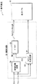
図1は、本技術の一実施の形態に係る表示装置1の概略構成を表したものである。この表示装置1は、表示パネル10と、外部から入力された映像信号Dinおよび同期信号Tinに基づいて表示パネル10を駆動する駆動回路20とを備えている。
<1. Embodiment>
[Constitution]
FIG. 1 illustrates a schematic configuration of a
(表示パネル10)
表示パネル10は、電圧印加により光の偏光状態を電気的に変えることで映像光を生成するものである。表示パネル10は、入力された映像信号Vsig1〜VsigNに基づいて入射光を変調することにより、映像を表示するものである。ここで、映像信号Vsig1〜VsigNは、相展開した映像信号である。表示パネル10がカラー表示用のパネルとなっている場合、映像信号Vsig1〜VsigNは、例えば、赤色用の画素に対応する映像信号VsigR1〜VsigRNと、緑色用の画素に対応する映像信号VsigG1〜VsigGNと、青色用の画素に対応する映像信号VsigB1〜VsigBNとを含んで構成されている。
(Display panel 10)
The
図2は、図1の表示パネル10の概略構成の一例を表したものである。表示パネル10は、例えば、パネル部11と、パネル部11に接続されたフレキシブルプリント基板(FPC:Flexible printed circuits)12(以下、FPC12と称する。)とを有している。パネル部11は、例えば、複数の画素14がマトリクス状に形成された画素領域13と、データ線駆動回路15と、走査線駆動回路16とを有している。パネル部11は、各画素14がデータ線駆動回路15および走査線駆動回路16によってアクティブ駆動されることにより、外部から入力されたデジタルの映像信号Dinに基づく映像を表示するものである。
FIG. 2 shows an example of a schematic configuration of the
パネル部11は、行方向に延在する複数の書込線WSLと、列方向に延在する複数の信号線DTLとを有している。信号線DTLと書込線WSLとの交差部分に対応して、画素14が設けられている。各信号線DTLは、データ線駆動回路15の出力端(図示せず)に接続されている。各書込線WSLは、走査線駆動回路16の出力端(図示せず)に接続されている。
The panel unit 11 has a plurality of write lines WSL extending in the row direction and a plurality of signal lines DTL extending in the column direction.
データ線駆動回路15は、例えば、駆動回路20から供給される1水平ライン分のアナログの映像信号を、各画素14に信号電圧として供給するものである。具体的には、データ線駆動回路15は、例えば、1水平ライン分のアナログの映像信号を、走査線駆動回路16により選択された1水平ラインを構成する各画素14に、信号線DTLを介してそれぞれ供給するものである。
For example, the data
走査線駆動回路16は、例えば、駆動回路20から供給される走査タイミング制御信号に応じて、駆動対象の画素14を選択するようになっている。具体的には、走査線駆動回路16は、例えば、走査線WSLを介して、選択パルスを画素14の選択回路(図示せず)に印加することにより、マトリックス状に配置されている複数の画素14のうちの1行を駆動対象として選択するようになっている。そして、これらの画素14では、データ線駆動回路15から供給される信号電圧に応じて、1水平ラインの表示がなされる。このようにして、走査線駆動回路16は、例えば、時分割的に1水平ラインずつ順次走査を行い、画素領域全体にわたった表示を行うようになっている。
For example, the scanning
(駆動回路20)
駆動回路20は、例えば、図1に示したように、信号処理回路30、タイミング生成回路40およびドライバ50を有している。
(Drive circuit 20)
The drive circuit 20 includes, for example, a
(信号処理回路30)
信号処理回路30は、映像信号Dinから、表示パネル10用の映像信号DAを生成するようになっている。映像信号Dinは、デジタルの映像信号であり、所定のγ補正のなされたものである。ここで、所定のγ補正とは、所定の表示装置(旧来はブラウン管テレビジョン)に映像信号Dinを入力したときに、映像信号Dinと、所定の表示装置の輝度との関係がリニアになるように補正することを指している。
(Signal processing circuit 30)
The
信号処理回路30は、映像信号Dinに対して所定の補正を行い、補正後の映像信号を、映像信号DAとして、ドライバ50に出力するようになっている。信号処理回路30は、さらに、同期信号Tinに含まれている水平同期信号および垂直同期信号に基づくタイミングで、映像信号DAをドライバ50に出力するようになっている。ここで、所定の補正としては、例えば、後述するように、リニアγ補正(または逆γ補正)や、γ補正、ムラ補正などが挙げられる。なお、所定の補正には、上記以外の補正が含まれていてもよい。ここで、リニアγ補正(または逆γ補正)とは、映像信号Dinのガンマ補正をキャンセルすることによりリニアなガンマ特性の映像信号(第3の映像信号)を生成することを指している。γ補正とは、特性がガンマ値に応じた最適のカーブとなるように映像信号の階調を補正することを指している。なお、ムラ補正については、後に詳述する。
The
図3は、信号処理回路30の内部構成の一部を表したものである。信号処理回路30は、例えば、リニアγ変換回路31、正規化回路32、ムラ補正回路33、階調化回路34、パネルγ変換回路35および記憶部36を有している。
FIG. 3 shows a part of the internal configuration of the
正規化回路32は、リニアγ変換回路31の出力信号(映像信号Din1)を正規化するものであり、映像信号Din1を正規化することにより得られた映像信号Din2を出力するようになっている。階調化回路34は、ムラ補正回路33の出力信号(映像信号Din3)に対して、後段のD/A変換回路52(後述)に適した階調情報を付与するものであり、ムラ補正回路33の出力信号(映像信号Din3)に対して所定の演算を行うことにより得られた映像信号Din4を出力するようになっている。
The
記憶部36は、例えば、リニアγ補正LUT36A、ムラ補正LUT36Bおよびγ補正LUT36Cを格納している。リニアγ補正LUT36Aは、出力信号のγ特性がリニアとなるように、入力信号と出力信号とを対応付けたものである。γ補正LUT36Cは、出力信号のγ特性が表示パネル10のγ特性と相補の関係となるように、入力信号と出力信号とを対応付けたものである。なお、ムラ補正LUT36Bについては、後に詳述する。
The
リニアγ変換回路31は、記憶部36から読み出したリニアγ補正LUT36Aを用いて、映像信号Dinを映像信号Din1に変換するものである。リニアγ変換回路31は、リニアγ補正LUT36Aを用いて、映像信号Dinのγ特性をリニアに変換し、映像信号Din1として、リニアのγ特性を有する映像信号を出力するようになっている。パネルγ変換回路35は、記憶部36から読み出したγ補正LUT36Cを用いて、映像信号Din4を映像信号DAに変換するものである。パネルγ変換回路35は、γ補正LUT36Cを用いて、映像信号Din4のリニアなγ特性を、表示パネル10のγ特性と相補の関係となるγ特性に変換し、映像信号DAとして、表示パネル10のγ特性と相補の関係となるγ特性を有する映像信号を出力するようになっている。
The linear
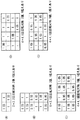
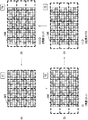
(ムラ補正LUT36B)
次に、ムラ補正LUT36Bについて説明する。図4(A)〜(G)は、ムラ補正LUT36Bを概念的に表したものであり、具体的には、ムラ補正LUT36Bに含まれる全ての補正係数を表示パネル10の画素14の配列に対応してマトリクス状に配列させたときの様子を表したものである。ムラ補正LUT36Bに含まれる複数の補正係数は、本来現れるはずの輝度に対して掛ける輝度比の値となっている。ここで、本来現れるはずの輝度とは、表示パネル10がカラー表示用のパネルとなっている場合には、画素14の発光色ごとの輝度を指している。従って、表示パネル10がカラー表示用のパネルとなっている場合、ムラ補正LUT36Bは、画素の色ごとに1つずつ設けられている。
(Unevenness correction LUT36B)
Next, the
図4(A)のムラ補正LUT36Bでは、4つの補正係数が2×2の行列となっており、2回回転対称の配置となっている。さらに、図4(A)のムラ補正LUT36Bでは、補正係数が2値となっており、かつ1未満(具体的には、0.9,0.95)となっている。図4(A)では、0.95の補正係数と0.9の補正係数とが対角に配置されている。図4(A)の配列が縦方向および横方向に繰り返し配置された場合には、0.95の補正係数が斜め方向に連続して延在すると共に、0.9の補正係数が斜め方向に連続して延在することになる。見方を変えると、0.95の補正係数と0.9の補正係数とが市松模様状に配置されている。従って、図4(A)の配列は、表示パネル10に起因して生じる特定のスジが縦方向または横方向に延在することを想定して設定されたものである。
In the
図4(B)のムラ補正LUT36Bでは、4つの補正係数が2×2の行列となっており、2回回転対称の配置となっている。さらに、図4(B)のムラ補正LUT36Bでは、補正係数が2値となっており、かつ1以下(具体的には、0.95,1)となっている。図4(B)では、0.95の補正係数と1の補正係数とが対角に配置されている。図4(B)の配列が縦方向および横方向に繰り返し配置された場合には、0.95の補正係数が斜め方向に連続して延在すると共に、1の補正係数が斜め方向に連続して延在することになる。見方を変えると、0.95の補正係数と1の補正係数とが市松模様状に配置されている。従って、図4(B)の配列は、表示パネル10に起因して生じる特定のスジが縦方向または横方向に延在することを想定して設定されたものである。
In the
図4(C)のムラ補正LUT36Bでは、12個の補正係数が6×2の行列となっており、1回回転対称の配置となっている。さらに、図4(C)のムラ補正LUT36Bでは、補正係数が3値となっており、かつ1以下(具体的には、0.9,0.95,1)となっている。図4(B)では、0.9の補正係数が2か所において、横一行に配置され、1の補正係数のブロックと0.95の補正係数のブロックとがそれぞれ、0.9の補正係数を中途に挟みながら、斜め方向に並んで配置されている。図4(C)の配列が縦方向および横方向に繰り返し配置された場合には、0.9の補正係数が横方向に連続して延在し、さらに、1の補正係数のブロックと0.95の補正係数のブロックとが斜め方向に並んで配置されることになる。そのため、表示パネル10に起因して生じる特定のスジが縦方向に延在している場合には、その特定のスジは、0.9の補正係数の延在方向と直交し、さらに、1の補正係数のブロックの配列と交差するとともに、0.95の補正係数のブロックの配列とも交差する。従って、図4(C)の配列は、表示パネル10に起因して生じる特定のスジが縦方向に延在することを想定して設定されたものである。
In the
図4(D)のムラ補正LUT36Bでは、16個の補正係数が4×4の行列となっており、1回回転対称の配置となっている。さらに、図4(D)のムラ補正LUT36Bでは、補正係数が3値となっており、かつ1以下(具体的には、0.9,0.95,1)となっている。図4(D)では、0.95および0.9の補正係数のブロックと、1の補正係数のブロックとが対角に配置されている。図4(D)の配列が縦方向および横方向に繰り返し配置された場合には、0.95および0.9の補正係数のブロックが斜め方向に連続して延在すると共に、1の補正係数のブロックが斜め方向に連続して延在することになる。見方を変えると、0.95および0.9の補正係数のブロックと1の補正係数のブロックとが市松模様状に配置されることになる。従って、図4(B)の配列は、表示パネル10に起因して生じる特定のスジが縦方向または横方向に延在することを想定して設定されたものである。
In the
図4(E)のムラ補正LUT36Bでは、16個の補正係数が4×4の行列となっており、1回回転対称の配置となっている。さらに、図4(E)のムラ補正LUT36Bでは、補正係数が2値となっており、かつ1未満(具体的には、0.9,0.95)となっている。図4(E)では、0.95の補正係数が多数敷き詰められているところに、0.9の補正係数がまばらに(離散して)配置されている。図4(E)の配列が縦方向および横方向に繰り返し配置された場合にも、0.95の補正係数が多数敷き詰められているところに、0.9の補正係数がまばらに(離散して)配置された態様となっている。従って、図4(E)の配列は、表示パネル10に起因して生じる特定のスジが縦方向、横方向または斜め方向に延在することを想定して設定されたものである。
In the
図4(F)のムラ補正LUT36Bでは、16個の補正係数が4×4の行列となっており、1回回転対称の配置となっている。さらに、図4(F)のムラ補正LUT36Bでは、補正係数が2値となっており、かつ1以下(具体的には、0.95,1)となっている。図4(F)では、0.95の補正係数が多数敷き詰められているところに、1の補正係数がまばらに(離散して)配置されている。図4(F)の配列が縦方向および横方向に繰り返し配置された場合にも、0.95の補正係数が多数敷き詰められているところに、1の補正係数がまばらに(離散して)配置された態様となっている。従って、図4(F)の配列は、表示パネル10に起因して生じる特定のスジが縦方向、横方向または斜め方向に延在することを想定して設定されたものである。
In the
図4(G)のムラ補正LUT36Bでは、16個の補正係数が4×4の行列となっており、1回回転対称の配置となっている。さらに、図4(G)のムラ補正LUT36Bでは、補正係数が3値となっており、かつ1以下(具体的には、0.9,0.95,1)となっている。図4(G)では、0.95の補正係数が多数敷き詰められているところに、1の補正係数と、0.9の補正係数とがまばらに(離散して)配置されている。図4(G)の配列が縦方向および横方向に繰り返し配置された場合にも、0.95の補正係数が多数敷き詰められているところに、1の補正係数と、0.9の補正係数とがまばらに(離散して)配置された態様となっている。従って、図4(G)の配列は、表示パネル10に起因して生じる特定のスジが縦方向、横方向または斜め方向に延在することを想定して設定されたものである。
In the
なお、ムラ補正LUT36Bに含まれる複数の補正係数のうち1種類の補正係数が、1よりも大きな整数値となっていてもよい。つまり、ムラ補正LUT36Bが、補正係数として、1よりも小さな整数、1、および1よりも大きな整数のうち、少なくとも、1および1よりも大きな整数を含んでいる。このようにした場合には、ムラ補正LUT36Bの適用による輝度低下を抑制することができる。図5(A)〜(E)は、補正係数として1よりも大きな整数値が含まれるムラ補正LUT36Bの配列の一例を表したものである。
Note that one type of correction coefficient among the plurality of correction coefficients included in the
図5(A)のムラ補正LUT36Bでは、4つの補正係数が2×2の行列となっており、2回回転対称の配置となっている。さらに、図5(A)のムラ補正LUT36Bでは、補正係数が2値となっており、かつ1を超える値(具体的には1.05)と1を含んでいる。図5(A)では、1の補正係数と1.05の補正係数とが対角に配置されている。図5(A)の配列が縦方向および横方向に繰り返し配置された場合には、1の補正係数が斜め方向に連続して延在すると共に、1.05の補正係数が斜め方向に連続して延在することになる。見方を変えると、1の補正係数と1.05の補正係数とが市松模様状に配置される。従って、図5(A)の配列は、表示パネル10に起因して生じる特定のスジが縦方向または横方向に延在することを想定して設定されたものである。
In the
図5(B)のムラ補正LUT36Bでは、12個の補正係数が6×2の行列となっており、1回回転対称の配置となっている。さらに、図5(B)のムラ補正LUT36Bでは、補正係数が3値となっており、かつ1を超える値(具体的には1.05)と、1以下の値(具体的には、0.95,1)とを含んでいる。図5(B)では、0.95の補正係数が2か所において、横一行に配置され、1の補正係数のブロックと1.05の補正係数のブロックとがそれぞれ、0.95の補正係数を中途に挟みながら、斜め方向に並んで配置されている。図5(B)の配列が縦方向および横方向に繰り返し配置された場合には、0.95の補正係数が横方向に連続して延在し、さらに、1の補正係数のブロックと0.95の補正係数のブロックとが斜め方向に並んで配置されることになる。そのため、表示パネル10に起因して生じる特定のスジが縦方向に延在している場合には、その特定のスジは、0.95の補正係数の延在方向と直交し、さらに、1の補正係数のブロックの配列と交差するとともに、0.95の補正係数のブロックの配列とも交差する。従って、図5(B)の配列は、表示パネル10に起因して生じる特定のスジが縦方向に延在することを想定して設定されたものである。
In the
図5(C)のムラ補正LUT36Bでは、16個の補正係数が4×4の行列となっており、1回回転対称の配置となっている。さらに、図5(C)のムラ補正LUT36Bでは、補正係数が3値となっており、かつ1を超える値(具体的には1.05)と、1以下の値(具体的には、0.95,1)とを含んでいる。図5(C)では、1.05の補正係数のブロックが斜め方向に並んで配置され、さらに、1の補正係数と0.95の補正係数とが配列中の所定の領域内で斜めに配置されている。従って、図5(C)の配列は、表示パネル10に起因して生じる特定のスジが縦方向または横方向に延在することを想定して設定されたものである。
In the
図5(D)のムラ補正LUT36Bでは、16個の補正係数が4×4の行列となっており、1回回転対称の配置となっている。さらに、図5(D)のムラ補正LUT36Bでは、補正係数が2値となっており、かつ1を超える値(具体的には1.05)と、1を含んでいる。図5(D)では、1の補正係数が多数敷き詰められているところに、1.05の補正係数がまばらに(離散して)配置されている。図5(D)の配列が縦方向および横方向に繰り返し配置された場合にも、1の補正係数が多数敷き詰められているところに、1.05の補正係数がまばらに(離散して)配置された態様となっている。従って、図5(D)の配列は、表示パネル10に起因して生じる特定のスジが縦方向、横方向または斜め方向に延在することを想定して設定されたものである。
In the
図5(E)のムラ補正LUT36Bでは、16個の補正係数が4×4の行列となっており、1回回転対称の配置となっている。さらに、図5(E)のムラ補正LUT36Bでは、補正係数が3値となっており、かつ1を超える値(具体的には1.05)と、1以下の値(具体的には、0.95,1)とを含んでいる。図5(E)では、1の補正係数と、0.95および1.05の補正係数のブロックとが配列中の所定の領域内で斜めに配置されている。従って、図5(E)の配列は、表示パネル10に起因して生じる特定のスジが縦方向、横方向または斜め方向に延在することを想定して設定されたものである。
In the
このように、ムラ補正LUT36Bは、表示パネル10の全画素数よりも少ない数の補正係数を含んで構成されている。ムラ補正LUT36Bは、さらに、ムラ補正LUT36Bに含まれる全ての補正係数を表示パネル10の画素14の配列に対応してマトリクス状に配列させたときの配列(以下、「第1配列」と称する。)において、列数が、表示パネル10の画素行の数よりも少なく、行数が、表示パネル10の画素列の数よりも少なくなっている。従って、ムラ補正回路33は、後述するように、ムラ補正LUT36Bを、表示パネル10の全画素に対応する階調信号に対して、一度にかけることはせず、ムラ補正LUT36Bに含まれる補正係数の数ごとに順次、かけるようになっている。
As described above, the
第1配列において、列数が、表示パネル10の画素行の数の約数と等しくなっていてもよいし(図6(A))、表示パネル10の画素行の数の約数と異なっていてもよい(図6(B))。また、第1配列において、行数が、表示パネル10の画素列の数の約数と等しくなっていてもよいし、表示パネル10の画素列の数の約数と異なっていてもよい。
In the first array, the number of columns may be equal to the divisor of the number of pixel rows of the display panel 10 (FIG. 6A), or different from the divisor of the number of pixel rows of the
第1配列の列数が、表示パネル10の画素行の数の約数と異なっている場合、ムラ補正回路33は、ムラ補正LUT36Bに含まれる全ての補正係数のうち、対応する画素14の無い補正係数については、演算を実施しないようになっている。同様に、第1配列の行数が、表示パネル10の画素列の数の約数と異なっている場合、ムラ補正回路33は、ムラ補正LUT36Bに含まれる全ての補正係数のうち、対応する画素14の無い補正係数については、演算を実施しないようになっている。
When the number of columns of the first array is different from the divisor of the number of pixel rows of the
また、ムラ補正LUT36Bは、ムラ補正LUT36Bに含まれる全ての補正係数を表示パネル10の画素14の配列に対応してマトリクス状に配列させると、点対称配列となっている。1回回転対称または2回回転対称の規則性を有している。なお、ムラ補正LUT36Bが、図4(A)〜(G)および図5(A)〜(E)に示された配列のうちいずれか1つの配列を2個以上組み合わせた配列となっていてもよい。
The
(ムラ補正回路33)
次に、ムラ補正回路33について説明する。図7〜図13は、ムラ補正回路33における演算の様子を模式的に表したものである。図7〜図13の左側には、ムラ補正回路33に入力される映像信号Din2が白表示に対応する映像信号となっていることが示されている。
(Unevenness correction circuit 33)
Next, the
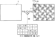
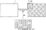
また、図7〜図13の中央には、ムラ補正回路33に入力される映像信号Din2と、ムラ補正LUT36Bとが互いに掛け合わされることが示されている。ここで、上述したように、ムラ補正LUT36Bは、表示パネル10の全画素数よりも少ない数の補正係数を含んで構成されている。そのため、ムラ補正回路33は、ムラ補正LUT36Bを、表示パネル10の全画素に対応する階調信号に対して、一度にかけることはせず、ムラ補正LUT36Bに含まれる補正係数の数ごとに順次、かけるようになっている。
7 to 13, the video signal Din2 input to the
また、図7〜図13の右側には、ムラ補正回路33から出力される映像信号Din3によって生成される映像が縞模様になっていることが示されている。なお、表示映像を生成するのは、ムラ補正回路33ではなく、表示パネル10である。また、映像信号Din3によって生成される映像には、規則性を有するノイズ状の模様がはっきりと描かれている。しかし、それは、誇張して表現されたものであり、実際の映像では、規則性を有するノイズ状の模様の輝度は、表示パネル10に起因して生じる複数のスジ(図14の左側の図を参照)と同レベルの輝度となっている。
Further, on the right side of FIGS. 7 to 13, it is shown that the video generated by the video signal Din3 output from the
なお、図7では、ムラ補正LUT36Bとして図4(A)に記載のものが用いられている。図8では、ムラ補正LUT36Bとして図4(B)に記載のものが用いられている。図9では、ムラ補正LUT36Bとして図4(C)に記載のものが用いられている。図10では、ムラ補正LUT36Bとして図4(D)に記載のものが用いられている。図11では、ムラ補正LUT36Bとして図4(E)に記載のものが用いられている。図12では、ムラ補正LUT36Bとして図4(F)に記載のものが用いられている。図13では、ムラ補正LUT36Bとして図4(G)に記載のものが用いられている。
In FIG. 7, the
ムラ補正回路33は、規則性を有するノイズ状の模様が映像に生成されるように映像信号Din2(第1の映像信号)に対して補正を行うことにより映像信号Din3(第2の映像信号)を生成するようになっている。具体的には、ムラ補正回路33は、ノイズ状の模様として、映像の面内の第1の方向、および第1の方向と交差する第2の方向に繰り返しパターンの模様が映像に生成されるように映像信号Din2に対して補正を行うことにより映像信号Din3を生成するようになっている。
The
ムラ補正回路33は、さらに、正規化回路32が映像信号Din1を正規化したのち、正規化後の映像信号Din2に対して、上述したように(すなわち、規則性を有するノイズ状の模様が映像に生成されるように)補正を行うことにより映像信号Din3を生成するようになっている。ここで、映像信号Din2は、表示パネル10の画素数分の階調信号を含んでいる。このとき、ムラ補正回路33は、表示パネル10の全画素数よりも少ない数の補正係数を含むムラ補正LUT36Bを用いて映像信号Din2の各階調信号に対して、上記の補正(以下、「ムラ補正」と称する。)を行うようになっている。つまり、ムラ補正LUT36Bは、低ビットのLUTである。
In addition, after the
例えば、ムラ補正回路33は、映像信号Din2の各階調信号に対する上記の補正を、ムラ補正LUT36Bに含まれる補正係数の数ごとに順次、行うようになっている。映像信号Din2の各階調信号に対する上記の補正とは、映像信号Din2の各階調信号に対して、ムラ補正LUT36Bに含まれる補正係数を掛けることを指している。その結果、図7〜図13に示したように、映像信号Din3に対応する映像には、規則性を有するノイズ状の模様が生成される。模様の周囲の白表示の輝度を1としたときに、規則性を有するノイズ状の模様の輝度は、例えば、0.95または0.9となっている。
For example, the
図14は、ムラ補正回路33における演算の様子の他の例を模式的に表したものである。図14の左側には、ムラ補正回路33に入力される映像信号Din2が白表示の中に複数のスジが存在するような映像信号となっていることが示されている。なお、図14には、ムラ補正LUT36Bとして図4(A)に記載のものが記載されているが、ムラ補正LUT36Bは、常に、図4(A)に記載のものに限定されるものではない。また、表示映像中の複数のスジは、白表示の中に存在するときには、わずかに視認できる程度のものである。
FIG. 14 schematically shows another example of the state of calculation in the
ムラ補正回路33は、映像信号Din2の階調の大きさや分布に拘わらず、規則性を有するノイズ状の模様が映像に生成されるように映像信号Din2に対して補正を行うことにより映像信号Din3を生成するようになっている。ムラ補正回路33は、さらに、正規化回路32が映像信号Din1を正規化したのち、正規化後の映像信号Din2に対して、映像信号Din2の階調の大きさや分布に拘わらず、上記の補正を行うことにより映像信号Din3を生成するようになっている。
The
ここで、映像信号Din2は、表示パネル10の画素数分の階調信号を含んでいる。このとき、ムラ補正回路33は、表示パネル10の全画素数よりも少ない数の補正係数を含むムラ補正LUT36Bを用いて映像信号Din2の各階調信号に対して、上記の補正を行うようになっている。例えば、ムラ補正回路33は、映像信号Din2の各階調信号に対する上記の補正を、ムラ補正LUT36Bに含まれる補正係数の数ごとに順次、行うようになっている。映像信号Din2の各階調信号に対する上記の補正とは、映像信号Din2の各階調信号に対して、ムラ補正LUT36Bに含まれる補正係数を掛けることを指している。
Here, the video signal Din2 includes gradation signals corresponding to the number of pixels of the
その結果、図14に示したように、映像信号Din3に対応する映像には、規則性を有するノイズ状の模様が生成される。つまり、白表示の中に複数のスジが存在するような映像に対して、規則性を有するノイズ状の模様が重畳される。これにより、表示映像中の複数のスジの輝度が、規則性を有するノイズ状の模様によってまだらに低減され、さらに、表示映像中の複数のスジ以外の部分の輝度も、規則性を有するノイズ状の模様によってまだらに低減される。なお、補正係数として1よりも高い数値が用いられている場合には、表示映像中の複数のスジの輝度が、規則性を有するノイズ状の模様によってまだらに低減されるとともにまだらに増加される。つまり、白表示の中に複数のスジが存在するような映像が、規則性を有するノイズ状の模様(ノイズ)によって乱される(荒らされる)。その結果として、表示映像中の複数のスジが、規則性を有するノイズ状の模様に溶け込んでしまうので、表示映像中の複数のスジを、ほとんど視認することができなくなる。 As a result, as shown in FIG. 14, a regular noise pattern is generated in the video corresponding to the video signal Din3. That is, a noise-like pattern having regularity is superimposed on an image in which a plurality of stripes are present in white display. As a result, the brightness of a plurality of streaks in the display image is mottled by the regular noise-like pattern, and the brightness of portions other than the plurality of streaks in the display image is also reduced to a regular noise state. The mottle is reduced by the pattern. When a numerical value higher than 1 is used as the correction coefficient, the luminance of a plurality of stripes in the display image is mottled and increased mottled by a noise-like pattern having regularity. . That is, an image in which a plurality of stripes are present in white display is disturbed (roughened) by a noise-like pattern (noise) having regularity. As a result, a plurality of streaks in the display image are melted into a regular noise pattern, so that the plurality of streaks in the display image can hardly be visually recognized.
以下で、信号処理回路30以外の構成(タイミング生成回路40、ドライバ50)について説明する。
Hereinafter, a configuration (
(タイミング生成回路40)
タイミング生成回路40は、制御信号Tinに含まれている水平同期信号および垂直同期信号に基づいて、液晶表示パネル10の駆動用タイミングパルスであって、かつ、水平、垂直の書き込み転送を制御するためのタイミングパルスTPを生成するようになっている。タイミング生成回路40は、生成したタイミングパルスTPを所定のタイミングで液晶表示パネル10に出力するようになっている。タイミング生成回路40は、タイミングパルスTPとして、例えば、水平走査の開始を指令する水平スタートパルス、水平走査の基準となる水平クロック、垂直走査の開始を指令する垂直スタートパルス、垂直走査の基準となる垂直クロックを生成するようになっている。タイミング生成回路40は、さらに、ドライバ50用のクロックCLKを生成し、ドライバ50に出力するようになっている。
(Timing generation circuit 40)
The
(ドライバ50)
図15は、ドライバ50を機能ブロックで表したものである。ドライバ50は、例えば、サンプル・ホールド回路51、D/A変換回路52、およびドライバ回路53を有している。サンプル・ホールド回路51は、シリアルデジタルの映像信号DAに対して並列化処理を行い、複数並列の映像信号に展開するようになっている。サンプル・ホールド回路51は、相展開した映像信号を、タイミング生成回路30からのクロックCLKに基づいたタイミングで、D/A変換回路52に出力するようになっている。D/A変換回路52は、サンプル・ホールド回路51から入力された映像信号(相展開した映像信号)をアナログ信号化して、ドライバ回路53に出力するようになっている。D/A変換回路52がドライバ回路53に出力する電圧の範囲が、表示パネル10の有効電圧範囲に対応する。つまり、D/A変換回路52が表示パネル10の有効電圧範囲を規定している。ドライバ回路53は、タイミング生成回路30から出力されたクロックCLKに基づく所定のタイミングで、アナログの映像信号を交流反転化させて、映像信号Vsig1〜VsigNとして、表示パネル10に印加するようになっている。
(Driver 50)
FIG. 15 shows the
[動作]
次に、表示装置1の動作(特に信号処理回路30の動作)について説明する。
[Operation]
Next, the operation of the display device 1 (particularly the operation of the signal processing circuit 30) will be described.
映像信号Dinが外部から入力されると、リニアγ変換回路31がリニアγ補正LUT36Aを用いて、映像信号Dinのγ特性をリニアに変換し、映像信号Din1として、リニアのγ特性を有する映像信号を出力する。次に、正規化回路32は、映像信号Din1を正規化することにより得られた映像信号Din2を出力する。次に、ムラ補正回路33は、表示パネル10の全画素数よりも少ない数の補正係数を含むムラ補正LUT36Bを用いて、映像信号Din2の各階調信号に対して補正を行う。具体的には、ムラ補正回路33は、表示パネル10の全画素に対応する階調信号に対して、ムラ補正LUT36Bに含まれる補正係数の数ごとに順次、かける。その後、ムラ補正回路33は、上記補正によって得られた映像信号Din3を出力する。
When the video signal Din is input from the outside, the linear
次に、階調化回路34は、映像信号Din3に対して、後段のD/A変換回路52に適した階調情報を付与する。具体的には、階調化回路34は、映像信号Din3に対して、ムラ補正LUT36Bに含まれる全ての補正係数を掛け、それにより得られた映像信号Din4を出力するようになっている。パネルγ変換回路35は、γ補正LUT36Cを用いて、映像信号Din4を映像信号DAに変換する。具体的には、パネルγ変換回路35は、γ補正LUT36Cを用いて、映像信号Din4のリニアなγ特性を、表示パネル10のγ特性と相補の関係となるγ特性に変換し、映像信号DAとして、表示パネル10のγ特性と相補の関係となるγ特性を有する映像信号を出力する。
Next, the
[効果]
次に、表示装置1の効果について説明する。表示装置1では、規則性を有するノイズ状の模様が映像に生成されるように映像信号Din2に対して補正を行うことにより映像信号Din3が生成される。これにより、表示パネル10に映像信号Din2が入力された場合の表示映像に、スジや輝度ムラが生じる場合であっても、その表示映像に、それらを目立たなくさせる模様を重畳させることができる。また、本技術では、表示映像に重畳される模様が、規則性を有するノイズ状の模様であり、表示パネル10の発光特性を測定することなく得られる模様である。従って、表示映像に上記の模様を重畳するために、表示パネル10の発光特性を測定する必要がない。これにより、スジや輝度ムラなどの表示不良を防止することができる。また、表示装置1では、表示映像に上記の模様を重畳するために、表示パネル10の発光特性を測定する必要がないので、製造時間を増大させる虞がない。以上のことから、本技術では、製造時間を増大させることなく表示不良を防止することができる。
[effect]
Next, the effect of the
<2.変形例>
[変形例1]
上記実施の形態では、ムラ補正回路33は、映像信号Din2の各階調信号に対するムラ補正を、ムラ補正LUT36Bに含まれる補正係数の数ごとに順次、行うようになっていた。このとき、ムラ補正回路33は、例えば、図6(A)または図6(B)に示したように、ムラ補正を一括して行う映像信号Din2の組み合わせを、時間経過に拘わらず固定にしてもよい。ただし、ムラ補正回路33は、ムラ補正を一括して行う映像信号Din2の組み合わせを、所定の時間ごとに変更するようにしてもよい。例えば、図16(A)、図16(B)、図16(C)および図16(D)にように、ムラ補正回路33は、ムラ補正を一括して行う映像信号Din2の組み合わせを、所定の時間ごとに、画素11配列の横方向に1画素分ずつずらすようにしてもよい。このようにした場合には、ムラ補正LUT36Bの適用によって生じる模様に起因する焼き付きを防止することができる。
<2. Modification>
[Modification 1]
In the above-described embodiment, the
[変形例2]
上記実施の形態では、信号処理回路30は、リニアγ変換回路31およびγ変換回路35を有していたが、例えば、図17に示したように、これらの省略することも可能である。つまり、信号処理回路30が、所定のγ補正がなされ、かつ正規化がなされていない映像信号Dinに対してムラ補正を行うようにしてもよい。
[Modification 2]
In the above-described embodiment, the
<3.適用例>
以下、上記実施の形態およびその変形例(以下、「上記実施の形態等」と称する。)で説明した表示装置1の適用例について説明する。上記実施の形態の表示装置1は、テレビジョン装置、デジタルカメラ、ノート型パーソナルコンピュータ、携帯電話等の携帯端末装置あるいはビデオカメラなど、外部から入力された映像信号あるいは内部で生成した映像信号を、画像あるいは映像として表示するあらゆる分野の電子機器の表示装置に適用することが可能である。
<3. Application example>
Hereinafter, application examples of the
(適用例1)
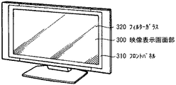
図18は、上記実施の形態等の表示装置1が適用されるテレビジョン装置の外観を表したものである。このテレビジョン装置は、例えば、フロントパネル310およびフィルターガラス320を含む映像表示画面部300を有しており、この映像表示画面部300は、上記実施の形態に係る表示装置1により構成されている。
(Application example 1)
FIG. 18 illustrates an appearance of a television device to which the
(適用例2)
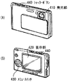
図19は、上記実施の形態等の表示装置1が適用されるデジタルカメラの外観を表したものである。このデジタルカメラは、例えば、フラッシュ用の発光部410、表示部420、メニュースイッチ430およびシャッターボタン440を有しており、その表示部420は、上記実施の形態等に係る表示装置1により構成されている。
(Application example 2)
FIG. 19 illustrates an appearance of a digital camera to which the
(適用例3)
図20は、上記実施の形態等の表示装置1が適用されるノート型パーソナルコンピュータの外観を表したものである。このノート型パーソナルコンピュータは、例えば、本体510,文字等の入力操作のためのキーボード520および画像を表示する表示部530を有しており、その表示部530は、上記実施の形態等に係る表示装置1により構成されている。
(Application example 3)
FIG. 20 illustrates an appearance of a notebook personal computer to which the
(適用例4)
図21は、上記実施の形態等の表示装置1が適用されるビデオカメラの外観を表したものである。このビデオカメラは、例えば、本体部610,この本体部610の前方側面に設けられた被写体撮影用のレンズ620,撮影時のスタート/ストップスイッチ630および表示部640を有しており、その表示部640は、上記実施の形態等に係る表示装置1により構成されている。
(Application example 4)
FIG. 21 illustrates an appearance of a video camera to which the
(適用例5)
図22は、上記実施の形態等の表示装置1が適用される携帯電話機の外観を表したものである。この携帯電話機は、例えば、上側筐体710と下側筐体720とを連結部(ヒンジ部)730で連結したものであり、ディスプレイ740,サブディスプレイ750,ピクチャーライト760およびカメラ770を有している。そのディスプレイ740またはサブディスプレイ750は、上記実施の形態等に係る表示装置1により構成されている。
(Application example 5)
FIG. 22 illustrates an appearance of a mobile phone to which the
以上、実施の形態および適用例を挙げて本発明を説明したが、本発明はこれらに限定されず、種々の変形が可能である。 Although the present invention has been described with reference to the embodiments and application examples, the present invention is not limited to these, and various modifications are possible.
例えば、上記実施の形態等において、信号処理回路30は、ハードウェア(回路)で構成されていてもよいし、ソフトウェア(プログラム)で構成されていてもよい。
For example, in the above embodiment and the like, the
また、上記実施の形態等では、表示装置1が有機EL表示装置である場合が例示されていたが、複数のμmオーダーのLEDが表示画素としてマトリクス状に配置されたLEDディスプレイであってもよい。LEDディスプレイにおいても、LED特性が個々のLEDによって異なることがあり、その場合には、表示映像に、スジや、輝度ムラが生じることがある。従って、本技術は、LEDディスプレイにおいても有効である。
Moreover, in the said embodiment etc., the case where the
また、例えば、本技術は以下のような構成を取ることができる。
(1)
規則性を有するノイズ状の模様が映像に生成されるように第1の映像信号に対して補正を行うことにより第2の映像信号を生成する
信号処理回路。
(2)
前記ノイズ状の模様として、前記映像の面内の第1の方向、および前記第1の方向と交差する第2の方向に繰り返しパターンの模様が前記映像に生成されるように前記第1の映像信号に対して補正を行うことにより前記第2の映像信号を生成する
(1)に記載の信号処理回路。
(3)
前記前記ノイズ状の模様のコントラストが、表示パネルの特性に起因して生じる筋状の模様のコントラストと同一もしくは同等か、またはそれよりも低くなるように、前記補正を行う
(1)または(2)に記載の信号処理回路。
(4)
前記第1の映像信号を正規化したのち、正規化後の第1の映像信号に対して前記補正を行うことにより前記第2の映像信号を生成する
(1)ないし(3)のいずれか1つに記載の信号処理回路。
(5)
前記第1の映像信号は、表示パネルの画素数分の階調信号を含み、
当該信号処理回路は、前記表示パネルの全画素数よりも少ない数の補正係数を含むLUT(Look Up Table)を用いて前記第1の映像信号の各階調信号に対して前記補正を行う
(4)に記載の信号処理回路。
(6)
前記第1の映像信号の各階調信号に対する前記補正を、前記LUTに含まれる補正係数の数ごとに順次、行う
(5)に記載の信号処理回路。
(7)
前記補正を一度に行う複数の階調信号の組み合わせを、所定の時間ごとに変更する
(5)または(6)に記載の信号処理回路。
(8)
前記LUTは、当該LUTに含まれる全ての補正係数を前記表示パネルの画素の配列に対応してマトリクス状に配列させたときに、その配列は、1回回転対称または2回回転対称となっている
(5)ないし(7)のいずれか1つに記載の信号処理回路。
(9)
前記LUTは、前記補正係数として、1よりも小さな整数、1、および1よりも大きな整数のうち、少なくとも、1および1よりも大きな整数を含む
(5)ないし(8)のいずれか1つに記載の信号処理回路。
(10)
前記第1の映像信号は、所定のガンマ補正のなされた映像信号であり、
当該信号処理回路は、前記第1の映像信号のガンマ補正をキャンセルすることによりリニアなガンマ特性の第3の映像信号を生成する
(1)ないし(9)のいずれか1つに記載の信号処理回路。
(11)
前記第3の映像信号を正規化したのち、正規化後の第3の映像信号に対して前記補正を行うことにより前記第2の映像信号を生成する
(10)に記載の信号処理回路。
(12)
表示パネルと、前記表示パネルを駆動する駆動回路とを備え、
前記駆動回路は、規則性を有するノイズ状の模様が映像に生成されるように第1の映像信号に対して補正を行うことにより第2の映像信号を生成する信号処理回路を有する
表示装置。
(13)
表示装置を備え、
前記表示装置は、表示パネルと、前記表示パネルを駆動する駆動回路とを有し、
前記駆動回路は、規則性を有するノイズ状の模様が映像に生成されるように第1の映像信号に対して補正を行うことにより第2の映像信号を生成する信号処理回路を有する
電子機器。
(14)
規則性を有するノイズ状の模様が映像に生成されるように第1の映像信号に対して補正を行うことにより第2の映像信号を生成する
信号補正方法。
For example, this technique can take the following composition.
(1)
A signal processing circuit that generates a second video signal by correcting the first video signal so that a noise-like pattern having regularity is generated in the video.
(2)
As the noise-like pattern, the first image is generated such that a pattern of a repetitive pattern is generated in the image in a first direction in the plane of the image and in a second direction intersecting the first direction. The signal processing circuit according to (1), wherein the second video signal is generated by correcting the signal.
(3)
The correction is performed so that the contrast of the noise-like pattern is the same as, equal to, or lower than the contrast of the streak-like pattern caused by the characteristics of the display panel (1) or (2 ) Signal processing circuit.
(4)
After normalizing the first video signal, the second video signal is generated by performing the correction on the first video signal after normalization. Any one of (1) to (3) The signal processing circuit according to one.
(5)
The first video signal includes gradation signals for the number of pixels of the display panel,
The signal processing circuit performs the correction on each gradation signal of the first video signal using an LUT (Look Up Table) including correction coefficients smaller than the total number of pixels of the display panel. ) Signal processing circuit.
(6)
The signal processing circuit according to (5), wherein the correction for each gradation signal of the first video signal is sequentially performed for each number of correction coefficients included in the LUT.
(7)
The signal processing circuit according to (5) or (6), wherein a combination of a plurality of gradation signals for performing the correction at a time is changed every predetermined time.
(8)
In the LUT, when all the correction coefficients included in the LUT are arranged in a matrix corresponding to the arrangement of the pixels of the display panel, the arrangement becomes one-time rotational symmetry or two-time rotational symmetry. The signal processing circuit according to any one of (5) to (7).
(9)
The LUT includes, as the correction coefficient, an integer smaller than 1, an integer larger than 1, and an integer larger than 1, and at least an integer larger than 1 and 1 (5) to (8) The signal processing circuit described.
(10)
The first video signal is a video signal subjected to a predetermined gamma correction,
The signal processing circuit generates a third video signal having a linear gamma characteristic by canceling gamma correction of the first video signal. Signal processing according to any one of (1) to (9) circuit.
(11)
The signal processing circuit according to (10), wherein after normalizing the third video signal, the second video signal is generated by performing the correction on the normalized third video signal.
(12)
A display panel and a drive circuit for driving the display panel;
The drive circuit includes a signal processing circuit that generates a second video signal by correcting the first video signal so that a noise-like pattern having regularity is generated in the video.
(13)
A display device,
The display device includes a display panel and a drive circuit that drives the display panel,
The electronic device includes a signal processing circuit that generates a second video signal by correcting the first video signal so that a noise-like pattern having regularity is generated in the video.
(14)
A signal correction method for generating a second video signal by correcting the first video signal so that a noise-like pattern having regularity is generated in the video.
1…表示装置、10…表示パネル、11…パネル部、12…FPC、13…画素領域、14…画素、15…データ線駆動回路、16…走査線駆動回路、20…駆動回路、30…信号処理回路、31…リニアγ変換回路、32…正規化回路、33…ムラ補正回路、34…階調化回路、35…パネルγ変換回路、36…記憶部、36A…リニアγ補正LUT、36B…ムラ補正LUT、36C…パネルγ補正LUT、40…タイミング生成回路、50…ドライバ、51…サンプル・ホールド回路、52…D/A変換回路、53…ドライバ回路、300…映像表示画面部、310…フロントパネル、320…フィルターガラス、410…発光部、420,530,640…表示部、430…メニュースイッチ、440…シャッターボタン、510…本体、520…キーボード、610…本体部、620…レンズ、630…スタート/ストップスイッチ、710…上側筐体、720…下側筐体、730…連結部、740…ディスプレイ、750…サブディスプレイ、760…ピクチャーライト、770…カメラ。
DESCRIPTION OF
Claims (13)
信号処理回路。 A signal processing circuit that generates a second video signal by correcting the first video signal so that a noise-like pattern having regularity is generated in the video.
請求項1に記載の信号処理回路。 As the noise-like pattern, the first image is generated such that a pattern of a repetitive pattern is generated in the image in a first direction in the plane of the image and in a second direction intersecting the first direction. The signal processing circuit according to claim 1, wherein the second video signal is generated by correcting the signal.
請求項2に記載の信号処理回路。 The signal processing circuit according to claim 2, wherein after normalizing the first video signal, the second video signal is generated by performing the correction on the first video signal after normalization.
当該信号処理回路は、前記表示パネルの全画素数よりも少ない数の補正係数を含むLUT(Look Up Table)を用いて前記第1の映像信号の各階調信号に対して前記補正を行う
請求項3に記載の信号処理回路。 The first video signal includes gradation signals for the number of pixels of the display panel,
The signal processing circuit performs the correction on each gradation signal of the first video signal by using an LUT (Look Up Table) including correction coefficients smaller than the total number of pixels of the display panel. 4. The signal processing circuit according to 3.
請求項4に記載の信号処理回路。 The signal processing circuit according to claim 4, wherein the correction for each gradation signal of the first video signal is sequentially performed for each number of correction coefficients included in the LUT.
請求項4に記載の信号処理回路。 The signal processing circuit according to claim 4, wherein a combination of a plurality of gradation signals for performing the correction at a time is changed every predetermined time.
請求項4に記載の信号処理回路。 In the LUT, when all the correction coefficients included in the LUT are arranged in a matrix corresponding to the arrangement of the pixels of the display panel, the arrangement becomes one-time rotational symmetry or two-time rotational symmetry. The signal processing circuit according to claim 4.
請求項3に記載の信号処理回路。 The signal processing circuit according to claim 3, wherein the LUT includes, as the correction coefficient, an integer smaller than 1, an integer larger than 1, and an integer larger than 1, and at least an integer larger than 1 and 1.
当該信号処理回路は、前記第1の映像信号のガンマ補正をキャンセルすることによりリニアなガンマ特性の第3の映像信号を生成する
請求項2に記載の信号処理回路。 The first video signal is a video signal subjected to a predetermined gamma correction,
The signal processing circuit according to claim 2, wherein the signal processing circuit generates a third video signal having a linear gamma characteristic by canceling gamma correction of the first video signal.
請求項9に記載の信号処理回路。 The signal processing circuit according to claim 9, wherein after normalizing the third video signal, the second video signal is generated by performing the correction on the normalized third video signal.
前記駆動回路は、規則性を有するノイズ状の模様が映像に生成されるように第1の映像信号に対して補正を行うことにより第2の映像信号を生成する信号処理回路を有する
表示装置。 A display panel and a drive circuit for driving the display panel;
The drive circuit includes a signal processing circuit that generates a second video signal by correcting the first video signal so that a noise-like pattern having regularity is generated in the video.
前記表示装置は、表示パネルと、前記表示パネルを駆動する駆動回路とを有し、
前記駆動回路は、規則性を有するノイズ状の模様が映像に生成されるように第1の映像信号に対して補正を行うことにより第2の映像信号を生成する信号処理回路を有する
電子機器。 A display device,
The display device includes a display panel and a drive circuit that drives the display panel,
The electronic device includes a signal processing circuit that generates a second video signal by correcting the first video signal so that a noise-like pattern having regularity is generated in the video.
信号補正方法。 A signal correction method for generating a second video signal by correcting the first video signal so that a noise-like pattern having regularity is generated in the video.
Priority Applications (3)
| Application Number | Priority Date | Filing Date | Title |
|---|---|---|---|
| JP2012170369A JP2014029428A (en) | 2012-07-31 | 2012-07-31 | Signal processing circuit, display device, electrical apparatus, and signal processing method |
| US13/938,341 US20140035962A1 (en) | 2012-07-31 | 2013-07-10 | Signal processing circuit, display unit, electronic apparatus, and signal processing method |
| CN201310314429.3A CN103578421A (en) | 2012-07-31 | 2013-07-24 | Signal processing circuit, display unit, electronic apparatus, and signal processing method |
Applications Claiming Priority (1)
| Application Number | Priority Date | Filing Date | Title |
|---|---|---|---|
| JP2012170369A JP2014029428A (en) | 2012-07-31 | 2012-07-31 | Signal processing circuit, display device, electrical apparatus, and signal processing method |
Publications (2)
| Publication Number | Publication Date |
|---|---|
| JP2014029428A true JP2014029428A (en) | 2014-02-13 |
| JP2014029428A5 JP2014029428A5 (en) | 2015-04-09 |
Family
ID=50025048
Family Applications (1)
| Application Number | Title | Priority Date | Filing Date |
|---|---|---|---|
| JP2012170369A Pending JP2014029428A (en) | 2012-07-31 | 2012-07-31 | Signal processing circuit, display device, electrical apparatus, and signal processing method |
Country Status (3)
| Country | Link |
|---|---|
| US (1) | US20140035962A1 (en) |
| JP (1) | JP2014029428A (en) |
| CN (1) | CN103578421A (en) |
Families Citing this family (4)
| Publication number | Priority date | Publication date | Assignee | Title |
|---|---|---|---|---|
| TW201411586A (en) * | 2012-09-06 | 2014-03-16 | Sony Corp | Image display device, driving method for image display device, signal generating device, signal generating program and signal generating method |
| WO2016031006A1 (en) * | 2014-08-28 | 2016-03-03 | Necディスプレイソリューションズ株式会社 | Display device, gradation correction map generation device, method and program for generating gradation correction map |
| US10755655B2 (en) * | 2018-01-17 | 2020-08-25 | Novatek Microelectronics Corp. | Source driver and operation method for improving display quality |
| WO2020158099A1 (en) * | 2019-01-31 | 2020-08-06 | 株式会社Jvcケンウッド | Image display device, image display system, and inspection method |
Citations (4)
| Publication number | Priority date | Publication date | Assignee | Title |
|---|---|---|---|---|
| JP2006038966A (en) * | 2004-07-23 | 2006-02-09 | Sony Corp | Image display device and driving method thereof |
| JP2006145798A (en) * | 2004-11-19 | 2006-06-08 | Hitachi Displays Ltd | Image signal display device |
| JP2008009318A (en) * | 2006-06-30 | 2008-01-17 | Toshiba Corp | Image processing apparatus and image processing method |
| WO2010064309A1 (en) * | 2008-12-03 | 2010-06-10 | 富士通株式会社 | Display and display control program |
Family Cites Families (2)
| Publication number | Priority date | Publication date | Assignee | Title |
|---|---|---|---|---|
| JP4400200B2 (en) * | 2003-12-10 | 2010-01-20 | セイコーエプソン株式会社 | Image display method, image display apparatus, and image display program |
| US8264613B2 (en) * | 2009-03-06 | 2012-09-11 | Radiant Zemax, Llc | Methods and systems for correcting streaming video signals |
-
2012
- 2012-07-31 JP JP2012170369A patent/JP2014029428A/en active Pending
-
2013
- 2013-07-10 US US13/938,341 patent/US20140035962A1/en not_active Abandoned
- 2013-07-24 CN CN201310314429.3A patent/CN103578421A/en active Pending
Patent Citations (4)
| Publication number | Priority date | Publication date | Assignee | Title |
|---|---|---|---|---|
| JP2006038966A (en) * | 2004-07-23 | 2006-02-09 | Sony Corp | Image display device and driving method thereof |
| JP2006145798A (en) * | 2004-11-19 | 2006-06-08 | Hitachi Displays Ltd | Image signal display device |
| JP2008009318A (en) * | 2006-06-30 | 2008-01-17 | Toshiba Corp | Image processing apparatus and image processing method |
| WO2010064309A1 (en) * | 2008-12-03 | 2010-06-10 | 富士通株式会社 | Display and display control program |
Also Published As
| Publication number | Publication date |
|---|---|
| US20140035962A1 (en) | 2014-02-06 |
| CN103578421A (en) | 2014-02-12 |
Similar Documents
| Publication | Publication Date | Title |
|---|---|---|
| US11335257B2 (en) | Display device and electronic apparatus | |
| KR100924142B1 (en) | Flat Panel Display device, Aging method and Lighting test method of the same | |
| TWI257603B (en) | Electro-optical device, driving circuit and driving method thereof, and electronic apparatus | |
| US8514209B2 (en) | Display apparatus and method for driving the same | |
| KR20210027628A (en) | Display device and driving method thereof | |
| US20150220194A1 (en) | Displays with Intra-Frame Pause | |
| JP2011039311A (en) | Display device, luminance deterioration correction method, and electronic device | |
| JP2010230999A (en) | Display panel and display | |
| CN104240638A (en) | Display apparatus and driving method thereof | |
| US8848003B2 (en) | Method of chromaticity adjustment of display device | |
| KR20130108054A (en) | Liquid crystal display apparatus, method of driving liquid crystal display apparatus, and electronic apparatus | |
| JP2011082213A (en) | Display panel, module, and electronic apparatus | |
| JP2014029428A (en) | Signal processing circuit, display device, electrical apparatus, and signal processing method | |
| CN102063864A (en) | Image display and image display method | |
| CN109377942B (en) | Display device compensation method and device and display equipment | |
| JP2011128442A (en) | Display panel, display device and electronic equipment | |
| US11823616B2 (en) | Display device | |
| KR20210024315A (en) | Display device and driving method thereof | |
| JP2011128443A (en) | Display device, method of driving the same, and electronic equipment | |
| JP6619622B2 (en) | Display panel, display device, and electronic device | |
| JP2009058725A (en) | Display device, method for driving display device, and electronic apparatus | |
| JP5903421B2 (en) | Display device | |
| KR102623354B1 (en) | Multi-vision device and display device included in multi-vision device | |
| JP2011145531A (en) | Display device, method for driving the same, and electronic equipment | |
| KR102170549B1 (en) | Display device |
Legal Events
| Date | Code | Title | Description |
|---|---|---|---|
| A521 | Request for written amendment filed |
Free format text: JAPANESE INTERMEDIATE CODE: A523 Effective date: 20150220 |
|
| A621 | Written request for application examination |
Free format text: JAPANESE INTERMEDIATE CODE: A621 Effective date: 20150220 |
|
| A977 | Report on retrieval |
Free format text: JAPANESE INTERMEDIATE CODE: A971007 Effective date: 20151225 |
|
| A131 | Notification of reasons for refusal |
Free format text: JAPANESE INTERMEDIATE CODE: A131 Effective date: 20160105 |
|
| A521 | Request for written amendment filed |
Free format text: JAPANESE INTERMEDIATE CODE: A523 Effective date: 20160218 |
|
| A02 | Decision of refusal |
Free format text: JAPANESE INTERMEDIATE CODE: A02 Effective date: 20160809 |