JP2013540059A5 - - Google Patents
Download PDFInfo
- Publication number
- JP2013540059A5 JP2013540059A5 JP2013517069A JP2013517069A JP2013540059A5 JP 2013540059 A5 JP2013540059 A5 JP 2013540059A5 JP 2013517069 A JP2013517069 A JP 2013517069A JP 2013517069 A JP2013517069 A JP 2013517069A JP 2013540059 A5 JP2013540059 A5 JP 2013540059A5
- Authority
- JP
- Japan
- Prior art keywords
- area
- layer
- region
- decorative
- area region
- Prior art date
- Legal status (The legal status is an assumption and is not a legal conclusion. Google has not performed a legal analysis and makes no representation as to the accuracy of the status listed.)
- Granted
Links
Images
Description
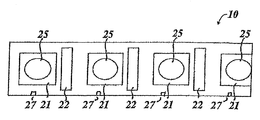
図1及び図2は、多数のエリア領域21及び22と、位置合わせマーク27とを備えた、転写ストリップ10の詳細を示す。この転写ストリップ10は、好ましくは、5mmから50mm、好ましくは15mmから30mmの幅の範囲で、転写ストリップ10の幅より好ましくは500倍大きい長さの、帯状の形状を有している。
1 and 2 show details of the
目標の基質の加飾の前に、形状が個別の機械的判読が可能な光学マークの形状に一致する、パターン状の接着層15が、それぞれエリア領域22上に印刷される。機械的判読が可能な光学マークは、ここでは、それぞれ一次元または二次元のバーコードから成ることが好ましい。従って、それらの接着層は、連続するエリア領域22に異なる接着パターンで印刷され、それぞれが、異なる一次元または二次元のバーコードの形状に一致する。
Prior to the decoration of the target substrate, a patterned adhesive layer 15 whose shape matches the shape of an individual mechanically readable optical mark is printed on each
接着層15は、ここでは、インクジェットプリンターで印刷されることが好ましい。このために、位置合わせ装置が、位置合わせマーク27を検出し、各エリア領域22に、それぞれ割り当てられた一次元または二次元バーコードのパターンを印刷するように、インクジェットプリンターヘッドを作動させる。
Here, the adhesive layer 15 is preferably printed by an inkjet printer. For this purpose, the alignment device detects the
特に好ましい実施形態では、レーザーにより脱色可能なカラー層及び/または照射によりカラー変化が誘発され得る層は、接着層14により形成される。その結果、よりシンプルでより薄い構造の転写ストリップ10が可能となる。
In a particularly preferred embodiment, the color layer detachable by laser and / or the layer whose color change can be induced by irradiation is formed by the adhesive layer 14. As a result, a simpler and
転写ストリップ10のエリア領域21は、図8に示すように、エリア領域213のように形成され、エリア領域22は、図8に示すように、エリア領域223のように形成される。エリア領域213では、ホログラムの成形レリーフ構造を備えた複製層と、部分的な金属反射層とが備えられる。上述したように、当然のことながら、割り当てられた多層体23に、光学活性層が備えられてもよい。エリア領域223には、20から60nmの間の層厚の、全エリアに亘る金属層、好ましくは、全エリアに亘るアルミニウム層が備えられる。レーザーにより、エリア領域223の金属層は、金属層が露光領域で蒸発するような露光強度と露光時間で、バーコードのネガ形態で露光される。その結果、図8において暗色で示される金属領域が、エリア領域223に残る。スタンピングエリア31及び32としてスタンピングエリア313及び323を備えたスタンピングツール30を用いた、図4及び図5に従う転写後、図8に示す加飾エレメント253の配置は、機械的判読が可能な光学マーク263に加えて、被加飾表面19に残る。
The
レーザーにより、続いて、エリア領域215が、二次元バーコードのネガ形態で露光される。露光強度及び黒色層の顔料は、ここでは、顔料が透明になるまで脱色され、露光領域における黒色層が透明になり、黒色の、不透明色効果が、露光されない領域のみに残る、という作用を、レーザーによる露光が有するように、選択される。その後に、加飾エレメント及び上述したように個別化される機械的判読が可能な光学マークの被加飾表面への転写が、図4及び図5に基づいて既に上述したように行われる。ここで、スタンピングツール30のスタンピングエリアは、図10に示すように、スタンピングエリア315のように形成される。転写後、加飾エレメント255及び個別の機械的判読が可能な光学マーク265の図10に示す配置が得られる。 The area area 215 is then exposed in the negative form of a two-dimensional barcode by means of a laser. The exposure intensity and pigment of the black layer are here decolored until the pigment is transparent, the black layer in the exposed area becomes transparent, and the black, opaque color effect remains only in the unexposed areas, It is chosen so that the exposure by the laser has. Thereafter, the transfer of the decorative element and the optically readable optical mark, which is individualized as described above, to the surface to be decorated is performed as already described above with reference to FIGS. Here, the stamping area of the stamping tool 30 is formed like a stamping area 315 as shown in FIG. After the transfer, the arrangement shown in FIG. 10 of the decorative element 255 and the optical marks 265 capable of individual mechanical interpretation is obtained.
部位107は、第一のエリア領域311が第二のエリア領域321を二つの外辺にのみ接して囲むオープンフレームを形成する配置を有する。これにより、第一のエリア領域と、第二のエリア領域とは、共に一つの矩形外径輪郭を形成し、第一のエリア領域311のエッジ長さが、二つのエリア領域の全体のエッジ長さを規定する。すなわち、第二のエリア領域321は、第一のエリア領域311の輪郭の内側に配置される。 The part 107 has an arrangement in which the first area region 311 forms an open frame surrounding the second area region 321 in contact with only two outer sides. As a result, the first area region and the second area region together form one rectangular outer diameter contour, and the edge length of the first area region 311 is the total edge length of the two area regions. Prescribe. That is, the second area region 321 is disposed inside the outline of the first area region 311.
Claims (15)
帯状の背面フィルム(11)と、加飾層(13)と、前記加飾層(13)と前記背面フィルム(11)との間に配置される剥離層(12)とを含む、転写ストリップ(10)を提供するステップで、
前記加飾層(13)が、同一の光学可変加飾エレメント(25、251〜255)を多数有し、前記加飾エレメントは第一のエリア領域(21、211〜215)に配置され、前記第一のエリア領域は互いに分離され、前記転写ストリップの長手方向において互いに間隔を開けて配置され、前記加飾層(13)が、第二のエリア領域(22、221〜225)を有し、前記第二のエリア領域は互いに分離され、前記転写ストリップの長手方向において互いに間隔を開けて配置され、前記加飾層(13)が、それぞれ異なる機械的判読が可能な光学マーク(26、261〜265)を提供する、一つ以上の特性化可能層を有し、
前記加飾層(13)の第一のエリア領域(21、211〜215)または第一のエリア領域(21、211〜215)の部分的領域と、第二のエリア領域(22、221〜225)または第二のエリア領域(22、221〜225)の部分的領域とを、被加飾表面(19)にそれぞれ転写するステップで、前記光学可変加飾エレメント(25、251〜255)の一つに加えて、特性化された機械的判読が可能な光学マーク(26、261〜265)が、前記転写ストリップ(10)から、前記被加飾表面(19)に転写されるように、前記第二のエリア領域(22、221〜225)それぞれの一つ以上の前記特性化可能層が、転写前または転写中に特性化される。 Surface (19) decoration method, in particular exterior decoration method, comprising the following steps:
A transfer strip comprising a strip-shaped back film (11), a decorative layer (13), and a release layer (12) disposed between the decorative layer (13) and the back film ( 11 ). 10) in the step of providing
The decoration layer (13) has many identical optical variable decoration elements (25, 251 to 255), the decoration elements are arranged in the first area region (21, 211 to 215), The first area regions are separated from each other and are spaced from each other in the longitudinal direction of the transfer strip, the decorative layer (13) has second area regions (22, 221 to 225), The second area regions are separated from each other and are spaced apart from each other in the longitudinal direction of the transfer strip, and the decorative layer (13) has optical marks (26, 261- 265) having one or more characterizable layers,
The first area area (21, 211-215) or the partial area of the first area area (21, 211-215) and the second area area (22, 221-225) of the decorative layer (13). ) Or a partial area of the second area area (22, 221 to 225), respectively, to the surface to be decorated (19), and one of the optical variable decoration elements (25, 251 to 255). In addition, the characterized mechanically readable optical marks (26, 261 to 265) are transferred from the transfer strip (10) to the decorated surface (19). One or more of the characterizable layers of each of the second area regions (22, 221-225) is characterized before or during transfer.
を特徴とする請求項1に記載の方法。 One or more of the characterizable layers for forming a one-dimensional barcode and / or a two-dimensional barcode is characterized as a characterized mechanically readable optical mark (26, 261-265). That
The method of claim 1, wherein:
前記加飾層が、前記第一のエリア領域(21、211〜215)及び/または前記第二のエリア領域において、レリーフ構造が表面に形成される複製層を、少なくともある領域で有し、この複製層が、特に、回折レリーフ構造、ホログラムのレリーフ構造、マクロ構造及び/またはレンズ構造、体積ホログラムを備える体積ホログラム層、薄膜層構造及び/またはコレステリック液晶を含む層を含み、及び/または、
前記光学可変加飾エレメント(25、251〜255)それぞれが、隠し情報を含み、この隠し情報が、確認エレメントにより、可視化され、及び/または、
前記第二のエリア領域(22、221〜225)における前記加飾層(13)が、カラーコーティング層、金属反射層、成形レリーフ構造を備える複製層、体積ホログラム層、薄膜層構造、及び/または液晶を含む層をそれぞれ含むこと、
を特徴とする請求項1または2のいずれか1項に記載の方法。 The decorative layer (13) includes one or more optically active layers in the first area region (21, 211 to 215) and / or the second area region, respectively. the interference and / or diffraction of the incident light according to the incident angle and / or viewing direction of the incident light, shows the different image information and / or different colors, and / or,
In the first area region (21, 211 to 215) and / or the second area region, the decorative layer has a replication layer on the surface of which a relief structure is formed at least in a certain region. The replication layer comprises in particular a diffractive relief structure, a hologram relief structure, a macro structure and / or a lens structure, a volume hologram layer comprising a volume hologram, a thin film layer structure and / or a layer comprising cholesteric liquid crystals, and / or
Each of the optically variable decorative elements (25, 251-255) includes hidden information, which is visualized by a confirmation element and / or
The decorative layer (13) in the second area region (22, 221 to 225) is a color coating layer, a metal reflective layer, a replication layer comprising a molded relief structure, a volume hologram layer, a thin film layer structure, and / or Each including a layer containing liquid crystal ,
The method according to any one of claims 1 or 2, characterized in.
を特徴とする請求項1から3のいずれか1項に記載の方法。 The first area areas (21, 211 to 215) are arranged with a certain distance from each other, and the first area areas (21, 211 to 215) are respectively arranged to be second area areas (22, 221). To 225), and the second area regions (22, 221 to 225) are arranged at a predetermined interval from each other, and are respectively located at the same position with respect to the assigned first area region. Being disposed on the transfer strip (10),
The method according to any one of claims 1 to 3 , characterized in that:
前記第一のエリア領域(21、211〜215)と前記第二のエリア領域(22、221〜225)とが互いに重ならず、好ましくは、前記第一のエリア領域(21、211〜215)それぞれが、前記第二のエリア領域(22、221〜225)それぞれと、少なくとも0.5mm、特に少なくとも1mm間隔を開けていること、
を特徴とする請求項1から4のいずれか1項に記載の方法。 It said second area region (22,221~225) is between 50 × 50 mm from 5 × 5 mm, preferably have a size between 20 × 20 mm from 10 × 10 mm, and / or,
The first area region (21, 211 to 215) and the second area region (22, 221 to 225) do not overlap each other, preferably the first area region (21, 211 to 215). Each spaced apart from each of the second area regions (22, 221-225) by at least 0.5mm, in particular at least 1mm ;
The method according to any one of claims 1 to 4 , characterized in that:
を特徴とする請求項1から5のいずれか1項に記載の方法。 The decorative layer (13) is different between one of the first area regions (21, 211 to 215) and the other second area region (22, 221 to 225). Having a sequence and / or having different layers,
A method according to any one of claims 1 to 5 , characterized in that
を特徴とする請求項1から6のいずれか1項に記載の方法。 During transfer, the transfer strip (10) is pressed against the surface to be decorated (19) by a stamping tool (30), the stamping tool being shaped in the decorative elements (25, 251 to 255). The raised first stamping area (31, 311 to 315) that matches the shape of the second raised stamping area that matches the shape of the second area region (22, 221 to 225) (32, 321 to 325 ), and before the transfer, the transfer strip (10) is moved by the alignment device so that the first stamping area (31, 311 to 315) is the first area region (21 the collides with the transfer strip (10) in the region of 211 to 215), the second stamping area (32,321~325) is To impinge on the transfer strip (10) in the region of the second area region (22,221~225) that are aligned with respect to the stamping tool (30),
The method according to any one of claims 1 to 6 , wherein:
を特徴とする請求項1から7のいずれか1項に記載の方法。 For characterization, on the surface of the decorative layer (13) opposite to the release layer (12), in the second area region (22, 221) or the second area region In the surface area of the surface to be decorated corresponding to the above, a pattern-like adhesive layer (15) is provided, and the shape of the pattern-like adhesive layer (15) is the optically readable mechanically characterized. In conformity with the shape of the mark, during transfer, the transfer strip ( 10 ) is applied to the surface to be decorated (19) in the second area region (22, 221) by a stamping tool (30). In the partial region where the patterned adhesive layer (15) is placed between the decorative layer (13) and the surface to be decorated (19) when pressed and peeled off, the characteristics The layer to be decorated is the surface to be decorated (1 In the other partial areas of the second area area (22, 221), the characterizable layer remains on the transfer strip (10) and when the surface to be decorated is peeled off. (19) being separated from the partial area remaining on;
A method according to any one of claims 1 to 7 , characterized in that
b)部分的な接着層(14)が、グラビア印刷またはスクリーン印刷により、前記部分的な接着層(14)が、前記第一のエリア領域(21、211)には備えられ、前記第二のエリア領域(22、221)には備えられないように、前記加飾層の前記剥離層(12)とは反対側の表面に印刷され、及び/または、
c)前記第二のエリア領域(22、221)または前記第二のエリア領域に対応する前記被加飾表面の表面領域において、前記パターン状の接着層(15)が、インクジェット印刷またはレーザー印刷により、前記加飾層(13)の前記剥離層(12)とは反対側の表面に印刷され、または、前記パターン状の接着層(15)が、熱転写印刷ヘッドにより、前記加飾層(13)の前記剥離層(12)とは反対側の表面に転写フィルムからパターン形態で転写されること、
を特徴とする請求項8に記載の方法。 a) the provided transfer strip ( 10 ) has a partial adhesive layer (14) applied to the surface of the decorative layer (13) opposite the release layer and the partial strip An adhesive layer (14) is provided in the first area region (21, 211) and not in the second area region (22, 221) , or
b) The partial adhesive layer (14) is provided in the first area region (21, 211) by gravure printing or screen printing, and the second area region (21, 211). Printed on the surface of the decorative layer opposite to the release layer (12) so as not to be provided in the area region (22, 221), and / or
c) In the surface area of the surface to be decorated corresponding to the second area area (22, 221) or the second area area, the patterned adhesive layer (15) is formed by inkjet printing or laser printing. The decorative layer (13) is printed on the surface opposite to the release layer (12), or the patterned adhesive layer (15) is applied to the decorative layer (13) by a thermal transfer printing head. Is transferred in a pattern form from a transfer film to the surface opposite to the release layer (12) .
9. The method of claim 8 , wherein:
を特徴とする請求項1から9のいずれか1項に記載の方法。 An adhesive layer is provided in the second area region (223, 225) on the surface of the decorative layer (13) opposite to the release layer (12), and one or more are provided for characterization. Characterization of the partial area is irradiated in a pattern form for ablation of these layers or to achieve a color change in these layers, Conform to the shape of the optically readable optical mark (26, 263, 265) or the negative shape of the characterized mechanically readable optical mark (26, 263, 265). During the transfer, the transfer strip (10) is applied to the entire surface area with respect to the surface to be decorated (19) by the stamping tool (30) in the second area region (22, 223, 225) Over Attached to, when the transfer strip is peeled off, the characterization can layer in said second area region (22,223,225) is to remain the on the decorative surface (19),
10. A method according to any one of claims 1 to 9 , characterized in that
を特徴とする請求項10に記載の方法。 A replication layer comprising a relief structure formed in at least a region is provided in the second area region, and one or more of the characterization layers are reflective layers, in particular metals, that increase the optical effect of the relief structure. Forming a reflective layer or an HRI layer, wherein the irradiation reduces the reflectivity of one or more of the characterizable layers in the irradiated partial region, particularly by ablation, and the optical effect of the relief structure Has the effect that in the irradiated partial area, it changes in its visual effect and in particular decreases.
The method according to claim 10 .
b)繊細な構造光学効果を生じる、例えば、繊細なモチーフ、ロゴ、または英数字を生じるレリーフ構造が、前記第一のエリア領域における前記加飾層の前記複製層に形成され、及び/または、大きな構造光学効果、特に、連続カラーグラデーションまたは表面カラー変化を生じるレリーフ構造が、前記第二のエリア領域における複製コーティング層に形成され、及びまたは、
c)前記加飾層が、前記第二のエリア領域において、複製層を有し、その表面には、各第二のエリア領域において、第一のレリーフ構造が、一つ以上の第一の部分的領域における少なくともある領域に形成されるとともに、少なくとも一つの構造パラメータが前記第一のレリーフ構造とは異なる第二のレリーフ構造が、一つ以上の第二の部分的領域に形成され、前記第二のエリア領域それぞれの前記特性化可能層が、前記第一の部分的領域及び前記第二の部分的領域双方において特性化され、特に、第一の照明条件下で判読可能であり、一つ以上の第一の部分的領域が形成される第一の部位と、前記第一の照明条件とは異なる第二の照明条件下で判読可能であり、一つ以上の第二の部分的領域が形成される第二の部位とを含む、特性化された機械的判読が可能な光学マークを提供し、及びまたは、
d)前記加飾層が、前記第一のエリア領域と前記第二のエリア領域とにおいて、表面の少なくともある領域にレリーフ構造が形成される複製層を有し、前記第一のエリア領域と前記第二のエリア領域とが互いに隣接する領域それぞれにおいて、静穏ゾーンが形成され、この静穏ゾーンでは、前記複製層にレリーフ構造、マット構造またはモスアイ構造が形成されず、及び/または、前記加飾層に備えられた一つ以上の前記反射層が完全に又はほとんど備えられず、または除去され、前記静穏ゾーンは、0.1mmから5mmの間、より好ましくは0.1mmから2mmの間の幅を好ましくは有すること、
を特徴とする請求項1から11のいずれか1項に記載の方法。 a) different relief structures are formed in the replication layer of the decorative layer in one of the first area regions and in the other second area region ; and / or
b) a relief structure that produces a delicate structural optical effect, for example a delicate motif, logo or alphanumeric character, is formed in the replication layer of the decorative layer in the first area region, and / or Relief structures that produce large structural optical effects, in particular continuous color gradations or surface color changes, are formed on the replica coating layer in the second area region and / or
c) The decorative layer has a replication layer in the second area region, and the first relief structure is formed on the surface of each of the second area regions by one or more first portions. A second relief structure formed in at least one region of the target region and having at least one structural parameter different from that of the first relief structure is formed in one or more second partial regions; The characterizable layer in each of the two area areas is characterized in both the first partial area and the second partial area, in particular readable under the first lighting conditions, The first portion where the first partial region is formed and the second partial illumination region can be read under a second illumination condition different from the first illumination condition, and the one or more second partial regions are Characterized, including a second site formed械的read to provide an optical mark capable of, and or,
d) The decorative layer has a replication layer in which a relief structure is formed in at least a region of the surface in the first area region and the second area region, and the first area region and the second area region A quiet zone is formed in each of the regions adjacent to each other in the second area region, and in this quiet zone, no relief structure, mat structure or moth-eye structure is formed in the replication layer, and / or the decorative layer One or more of the reflective layers provided in the substrate is completely or hardly provided or removed, and the quiet zone preferably has a width between 0.1 mm and 5 mm, more preferably between 0.1 mm and 2 mm. Having
12. The method according to any one of claims 1 to 11 , characterized by:
を特徴とする請求項1から12のいずれか1項に記載の方法。 On the surface of the decorative layer (13) opposite to the release layer (12), at least in the first area region (21, 211 to 215), preferably at least the first area region and In the second area region, an adhesive layer (14) is applied over the entire surface area, in particular by screen printing or gravure printing, and during transfer, the transfer strip (10) is in contact with the first area region. (21, 211-215), the stamping tool (30) matching the shape of the decorative element (25, 251-255) is pressed against the surface to be decorated (19), and the transfer strip ( 10) is peeled from the surface to be decorated (19), and thus when the peeling is performed, the decorative element (25, 251 to 255) is moved forward. Together remain on the decorated surface (19), said remaining on the peripheral region of the transfer strip of the decorative layer (13) (10), said being separated from the decorative element (25,251~255)
13. A method according to any one of claims 1 to 12 , characterized in that
前記加飾層(13)が、同一の光学可変加飾エレメント(25、251〜255)を多数有し、前記加飾エレメントは第一のエリア領域(21、211〜215)に配置され、前記第一のエリア領域は互いに分離され、前記転写ストリップ(10)の長手方向において互いに間隔を開けて配置され、
前記加飾層(13)が、第二のエリア領域(22、221〜225)を有し、前記第二のエリア領域は互いに分離され、前記転写ストリップ(10)の長手方向において互いに間隔を開けて配置され、
前記第二のエリア領域において、前記加飾層(13)が、それぞれ異なる機械的判読が可能な光学マーク(26、261〜265)を提供する、一つ以上の特性化可能層を有する、転写ストリップ。 A transfer strip (10) for decorating the surface, in particular for decorating the exterior, wherein the transfer strip (10) comprises a strip-shaped back film (11), a decoration layer (13), and the decoration A release layer (12) disposed between the layer and the back film,
The decoration layer (13) has many identical optical variable decoration elements (25, 251 to 255), the decoration elements are arranged in the first area region (21, 211 to 215), The first area regions are separated from each other and are spaced apart from each other in the longitudinal direction of the transfer strip (10),
The decorative layer (13) has second area areas (22, 221 to 225), the second area areas are separated from each other and spaced from each other in the longitudinal direction of the transfer strip (10). Arranged,
In the second area area, the decorative layer (13) has one or more characterizable layers that provide different mechanically readable optical marks (26, 261 to 265), respectively. strip.
Applications Claiming Priority (5)
| Application Number | Priority Date | Filing Date | Title |
|---|---|---|---|
| DE102010025278A DE102010025278A1 (en) | 2010-06-28 | 2010-06-28 | Method for decorating outer packages of cigarettes, involves individualizing layers of surface region before or during transfer of surface region, so that machine-readable optical mark is transferred to surface to be decorated |
| DE102010025278.6 | 2010-06-28 | ||
| DE102010048817 | 2010-10-20 | ||
| DE102010048817.8 | 2010-10-20 | ||
| PCT/EP2011/003126 WO2012000631A2 (en) | 2010-06-28 | 2011-06-24 | Method for decorating surfaces |
Publications (3)
| Publication Number | Publication Date |
|---|---|
| JP2013540059A JP2013540059A (en) | 2013-10-31 |
| JP2013540059A5 true JP2013540059A5 (en) | 2014-08-14 |
| JP5744194B2 JP5744194B2 (en) | 2015-07-01 |
Family
ID=45402475
Family Applications (1)
| Application Number | Title | Priority Date | Filing Date |
|---|---|---|---|
| JP2013517069A Active JP5744194B2 (en) | 2010-06-28 | 2011-06-24 | Surface decoration method |
Country Status (9)
| Country | Link |
|---|---|
| US (1) | US8932425B2 (en) |
| EP (2) | EP3339052B1 (en) |
| JP (1) | JP5744194B2 (en) |
| CN (1) | CN103025540B (en) |
| ES (1) | ES2665041T3 (en) |
| MX (2) | MX342719B (en) |
| PL (1) | PL3339052T3 (en) |
| RS (1) | RS57130B1 (en) |
| WO (1) | WO2012000631A2 (en) |
Families Citing this family (23)
| Publication number | Priority date | Publication date | Assignee | Title |
|---|---|---|---|---|
| EP2579217A1 (en) * | 2011-10-04 | 2013-04-10 | Deutsche Post AG | Method and device for marking value labels |
| DE102012105342A1 (en) * | 2012-06-20 | 2013-12-24 | Kba-Notasys Sa | Method for transferring a decorative section of a stamping foil |
| DE102012015695A1 (en) * | 2012-07-31 | 2014-06-12 | Benjamin Sieben | Method for retrieving information over quick response codes by electronic devices, particularly smartphones, involves supplementing quick response codes by code consisting of characters and numbers |
| CN104021409B (en) * | 2013-02-28 | 2017-03-01 | 国际商业机器公司 | The method and apparatus of automatic conversion mark and the automatic method reading mark |
| DE102014112073A1 (en) | 2014-08-22 | 2016-02-25 | Ovd Kinegram Ag | Transfer film and method for producing a transfer film |
| DE102015112909B3 (en) | 2015-08-05 | 2017-02-09 | Leonhard Kurz Stiftung & Co. Kg | Method and device for producing a multilayer film |
| KR101729683B1 (en) * | 2015-09-16 | 2017-04-25 | 한국기계연구원 | Manufacturing method of wire grid polarizer |
| TWI764875B (en) * | 2015-11-03 | 2022-05-21 | 德商利昂哈德 庫爾茲公司 | Method for applying a transfer layer on a film to a substrate and an application device therefor |
| WO2017131499A1 (en) | 2016-01-27 | 2017-08-03 | 주식회사 엘지화학 | Film mask, method for manufacturing same, and method for forming pattern using film mask and pattern formed thereby |
| EP3410213B1 (en) | 2016-01-27 | 2021-05-26 | LG Chem, Ltd. | Film mask, method for manufacturing same, and method for forming pattern using film mask |
| KR102138960B1 (en) | 2016-01-27 | 2020-07-28 | 주식회사 엘지화학 | Film mask, preparing method thereof, pattern forming method using the same and pattern formed by using the same |
| US9892288B2 (en) * | 2016-02-24 | 2018-02-13 | Modagrafics | Process for manufacturing decorative multilayer coatings method of use thereof |
| US10112378B2 (en) * | 2016-05-24 | 2018-10-30 | Chem Etch Manufacturing Inc. | Method of manufacturing anti-theft labels |
| EP3378671A1 (en) * | 2017-03-24 | 2018-09-26 | Authentic Vision GmbH | Security foil |
| DE102017110892A1 (en) | 2017-05-18 | 2018-11-22 | Kurz Digital Solutions Gmbh & Co. Kg | Method for authenticating an item, in particular a security item, and security item |
| DE102017115804A1 (en) * | 2017-07-13 | 2019-01-17 | Mayr-Melnhof Karton Ag | Method and apparatus for producing a coated substrate, tool, coated substrate and packaging |
| JP6836787B2 (en) * | 2017-08-02 | 2021-03-03 | プラス株式会社 | Transfer tape |
| CN107933064B (en) * | 2017-11-10 | 2019-05-07 | 上海天马微电子有限公司 | A kind of transfer substrate and preparation method thereof |
| JP2021524396A (en) * | 2018-05-25 | 2021-09-13 | オーファウデー キネグラム アーゲー | Method for manufacturing laminate and laminate film, laminate and laminate film |
| DE102018005697A1 (en) | 2018-07-19 | 2020-01-23 | Giesecke+Devrient Currency Technology Gmbh | Security element with lenticular image |
| CN111716936B (en) * | 2019-03-19 | 2021-08-06 | 中钞特种防伪科技有限公司 | Optical anti-counterfeiting element and optical anti-counterfeiting product |
| EP4050387A4 (en) * | 2019-10-23 | 2023-11-22 | Zeon Corporation | Liquid crystal cured layer transfer seal, liquid crystal cured layer transfer matter, and method for assessing authenticity of liquid crystal cured layer transfer seal |
| NL2032705B1 (en) * | 2022-08-09 | 2024-02-16 | Northann Building Solutions LLC | Computer-implemented method for generating a decorative pattern for decorative panels, and manufacturing method of such panels |
Family Cites Families (9)
| Publication number | Priority date | Publication date | Assignee | Title |
|---|---|---|---|---|
| DE3932505C2 (en) * | 1989-09-28 | 2001-03-15 | Gao Ges Automation Org | Data carrier with an optically variable element |
| JPH03114877A (en) * | 1989-09-29 | 1991-05-16 | Toppan Printing Co Ltd | Stamping wheel |
| DE4433858C1 (en) * | 1994-09-22 | 1996-05-09 | Kurz Leonhard Fa | transfer sheet |
| DE29807638U1 (en) * | 1998-04-28 | 1998-08-06 | Kurz Leonhard Fa | Embossing foil with individually identified security features |
| JP2002200871A (en) * | 2000-10-24 | 2002-07-16 | Konica Corp | Image recording body, forming method thereof and authentication discriminating method using thereof |
| ITMI20011195A1 (en) * | 2001-06-06 | 2002-12-06 | Veneta Decalcogomme S R L | PROCEDURE FOR MAKING A HOT-TRANSFERABLE DECORATIVE FILM ON A FLEXIBLE SUPPORT TAPE |
| DE10241803A1 (en) * | 2002-09-06 | 2004-03-18 | Erich Utsch Ag | Procedure for manufacturing of high security number plates entails colouring raised areas of embossed backing plate by at least partial transfer of decorative layer from embossed film onto backing plate |
| DE10251781A1 (en) * | 2002-11-05 | 2004-05-19 | Giesecke & Devrient Gmbh | Security element, for chip cards and security documents and currency notes, has a holograph refraction pattern formed by a carrier bonded to a substrate with surface structures |
| JP5608891B2 (en) * | 2009-07-28 | 2014-10-22 | シクパ ホルディング ソシエテ アノニムSicpa Holding Sa | Transfer foil containing optically changing magnetic pigment, method of manufacturing transfer foil, use of transfer foil, and article or document comprising transfer foil |
-
2011
- 2011-06-24 PL PL18151556.0T patent/PL3339052T3/en unknown
- 2011-06-24 JP JP2013517069A patent/JP5744194B2/en active Active
- 2011-06-24 MX MX2016002683A patent/MX342719B/en unknown
- 2011-06-24 WO PCT/EP2011/003126 patent/WO2012000631A2/en active Application Filing
- 2011-06-24 RS RS20180442A patent/RS57130B1/en unknown
- 2011-06-24 MX MX2012014792A patent/MX339573B/en active IP Right Grant
- 2011-06-24 EP EP18151556.0A patent/EP3339052B1/en active Active
- 2011-06-24 US US13/807,170 patent/US8932425B2/en active Active
- 2011-06-24 EP EP11727928.1A patent/EP2585314B1/en active Active
- 2011-06-24 CN CN201180036744.3A patent/CN103025540B/en active Active
- 2011-06-24 ES ES11727928.1T patent/ES2665041T3/en active Active
Similar Documents
| Publication | Publication Date | Title |
|---|---|---|
| JP2013540059A5 (en) | ||
| JP5744194B2 (en) | Surface decoration method | |
| RU2374082C2 (en) | Method for manufacturing of multi-layer substrate and multi-layer substrate | |
| JP5811484B2 (en) | Multilayer element manufacturing method and multilayer element | |
| TWI474935B (en) | Verfahren zur herstellung eines folienelements | |
| JP5124575B2 (en) | Method for producing multilayer body and multilayer body | |
| JP3883232B2 (en) | Method of manufacturing a partially transparent security element | |
| RU2422572C2 (en) | Protection element for protected document and method of its fabrication | |
| ES2576679T3 (en) | Holographic security element and method for its production | |
| CN105431302B (en) | Prepare the method and polylayer forest of polylayer forest | |
| JP7294380B2 (en) | Information display medium and related manufacturing method | |
| CA2930911C (en) | Multi-layer body and method for the production thereof | |
| JP2005530186A (en) | Multi-layer image, especially multi-layer color image | |
| JP2015061753A (en) | Manufacturing process of multilayer product, and multilayer product | |
| JP2003150027A (en) | Hologram sheet for metallic vapor deposition type hot printing, and its processing method | |
| JP2011501817A5 (en) | ||
| DE102010025278A1 (en) | Method for decorating outer packages of cigarettes, involves individualizing layers of surface region before or during transfer of surface region, so that machine-readable optical mark is transferred to surface to be decorated | |
| TW202122279A (en) | Decorative foil, method for producing a decorative foil and method for decorating a target substrate | |
| KR100247850B1 (en) | Security device, embossing table for security device and the preparation method of security device | |
| JP3227763U (en) | Diffraction grating sheet with visible pattern | |
| JP2009157287A (en) | Manufacturing method of diffraction structure formation body | |
| JP2009128475A (en) | Manufacturing method of security optical device and security optical device | |
| JP2014071125A (en) | Material with hologram image formed thereon |