JP2013534026A - Confinement layer and methods and materials for manufacturing devices manufactured using the same - Google Patents
Confinement layer and methods and materials for manufacturing devices manufactured using the same Download PDFInfo
- Publication number
- JP2013534026A JP2013534026A JP2013515506A JP2013515506A JP2013534026A JP 2013534026 A JP2013534026 A JP 2013534026A JP 2013515506 A JP2013515506 A JP 2013515506A JP 2013515506 A JP2013515506 A JP 2013515506A JP 2013534026 A JP2013534026 A JP 2013534026A
- Authority
- JP
- Japan
- Prior art keywords
- layer
- undercoat
- group
- formula
- active layer
- Prior art date
- Legal status (The legal status is an assumption and is not a legal conclusion. Google has not performed a legal analysis and makes no representation as to the accuracy of the status listed.)
- Pending
Links
Images


Classifications
-
- G—PHYSICS
- G03—PHOTOGRAPHY; CINEMATOGRAPHY; ANALOGOUS TECHNIQUES USING WAVES OTHER THAN OPTICAL WAVES; ELECTROGRAPHY; HOLOGRAPHY
- G03F—PHOTOMECHANICAL PRODUCTION OF TEXTURED OR PATTERNED SURFACES, e.g. FOR PRINTING, FOR PROCESSING OF SEMICONDUCTOR DEVICES; MATERIALS THEREFOR; ORIGINALS THEREFOR; APPARATUS SPECIALLY ADAPTED THEREFOR
- G03F7/00—Photomechanical, e.g. photolithographic, production of textured or patterned surfaces, e.g. printing surfaces; Materials therefor, e.g. comprising photoresists; Apparatus specially adapted therefor
- G03F7/004—Photosensitive materials
- G03F7/027—Non-macromolecular photopolymerisable compounds having carbon-to-carbon double bonds, e.g. ethylenic compounds
-
- B—PERFORMING OPERATIONS; TRANSPORTING
- B05—SPRAYING OR ATOMISING IN GENERAL; APPLYING FLUENT MATERIALS TO SURFACES, IN GENERAL
- B05D—PROCESSES FOR APPLYING FLUENT MATERIALS TO SURFACES, IN GENERAL
- B05D3/00—Pretreatment of surfaces to which liquids or other fluent materials are to be applied; After-treatment of applied coatings, e.g. intermediate treating of an applied coating preparatory to subsequent applications of liquids or other fluent materials
- B05D3/06—Pretreatment of surfaces to which liquids or other fluent materials are to be applied; After-treatment of applied coatings, e.g. intermediate treating of an applied coating preparatory to subsequent applications of liquids or other fluent materials by exposure to radiation
-
- G—PHYSICS
- G03—PHOTOGRAPHY; CINEMATOGRAPHY; ANALOGOUS TECHNIQUES USING WAVES OTHER THAN OPTICAL WAVES; ELECTROGRAPHY; HOLOGRAPHY
- G03F—PHOTOMECHANICAL PRODUCTION OF TEXTURED OR PATTERNED SURFACES, e.g. FOR PRINTING, FOR PROCESSING OF SEMICONDUCTOR DEVICES; MATERIALS THEREFOR; ORIGINALS THEREFOR; APPARATUS SPECIALLY ADAPTED THEREFOR
- G03F7/00—Photomechanical, e.g. photolithographic, production of textured or patterned surfaces, e.g. printing surfaces; Materials therefor, e.g. comprising photoresists; Apparatus specially adapted therefor
- G03F7/26—Processing photosensitive materials; Apparatus therefor
- G03F7/40—Treatment after imagewise removal, e.g. baking
- G03F7/405—Treatment with inorganic or organometallic reagents after imagewise removal
-
- H—ELECTRICITY
- H10—SEMICONDUCTOR DEVICES; ELECTRIC SOLID-STATE DEVICES NOT OTHERWISE PROVIDED FOR
- H10K—ORGANIC ELECTRIC SOLID-STATE DEVICES
- H10K50/00—Organic light-emitting devices
-
- H—ELECTRICITY
- H10—SEMICONDUCTOR DEVICES; ELECTRIC SOLID-STATE DEVICES NOT OTHERWISE PROVIDED FOR
- H10K—ORGANIC ELECTRIC SOLID-STATE DEVICES
- H10K50/00—Organic light-emitting devices
- H10K50/10—OLEDs or polymer light-emitting diodes [PLED]
- H10K50/14—Carrier transporting layers
- H10K50/15—Hole transporting layers
-
- H—ELECTRICITY
- H10—SEMICONDUCTOR DEVICES; ELECTRIC SOLID-STATE DEVICES NOT OTHERWISE PROVIDED FOR
- H10K—ORGANIC ELECTRIC SOLID-STATE DEVICES
- H10K50/00—Organic light-emitting devices
- H10K50/10—OLEDs or polymer light-emitting diodes [PLED]
- H10K50/17—Carrier injection layers
-
- H—ELECTRICITY
- H10—SEMICONDUCTOR DEVICES; ELECTRIC SOLID-STATE DEVICES NOT OTHERWISE PROVIDED FOR
- H10K—ORGANIC ELECTRIC SOLID-STATE DEVICES
- H10K50/00—Organic light-emitting devices
- H10K50/80—Constructional details
-
- H—ELECTRICITY
- H10—SEMICONDUCTOR DEVICES; ELECTRIC SOLID-STATE DEVICES NOT OTHERWISE PROVIDED FOR
- H10K—ORGANIC ELECTRIC SOLID-STATE DEVICES
- H10K71/00—Manufacture or treatment specially adapted for the organic devices covered by this subclass
-
- H—ELECTRICITY
- H10—SEMICONDUCTOR DEVICES; ELECTRIC SOLID-STATE DEVICES NOT OTHERWISE PROVIDED FOR
- H10K—ORGANIC ELECTRIC SOLID-STATE DEVICES
- H10K71/00—Manufacture or treatment specially adapted for the organic devices covered by this subclass
- H10K71/10—Deposition of organic active material
- H10K71/12—Deposition of organic active material using liquid deposition, e.g. spin coating
- H10K71/13—Deposition of organic active material using liquid deposition, e.g. spin coating using printing techniques, e.g. ink-jet printing or screen printing
-
- H—ELECTRICITY
- H10—SEMICONDUCTOR DEVICES; ELECTRIC SOLID-STATE DEVICES NOT OTHERWISE PROVIDED FOR
- H10K—ORGANIC ELECTRIC SOLID-STATE DEVICES
- H10K85/00—Organic materials used in the body or electrodes of devices covered by this subclass
- H10K85/10—Organic polymers or oligomers
- H10K85/111—Organic polymers or oligomers comprising aromatic, heteroaromatic, or aryl chains, e.g. polyaniline, polyphenylene or polyphenylene vinylene
-
- C—CHEMISTRY; METALLURGY
- C08—ORGANIC MACROMOLECULAR COMPOUNDS; THEIR PREPARATION OR CHEMICAL WORKING-UP; COMPOSITIONS BASED THEREON
- C08G—MACROMOLECULAR COMPOUNDS OBTAINED OTHERWISE THAN BY REACTIONS ONLY INVOLVING UNSATURATED CARBON-TO-CARBON BONDS
- C08G2261/00—Macromolecular compounds obtained by reactions forming a carbon-to-carbon link in the main chain of the macromolecule
- C08G2261/30—Monomer units or repeat units incorporating structural elements in the main chain
- C08G2261/31—Monomer units or repeat units incorporating structural elements in the main chain incorporating aromatic structural elements in the main chain
- C08G2261/316—Monomer units or repeat units incorporating structural elements in the main chain incorporating aromatic structural elements in the main chain bridged by heteroatoms, e.g. N, P, Si or B
- C08G2261/3162—Arylamines
-
- C—CHEMISTRY; METALLURGY
- C08—ORGANIC MACROMOLECULAR COMPOUNDS; THEIR PREPARATION OR CHEMICAL WORKING-UP; COMPOSITIONS BASED THEREON
- C08G—MACROMOLECULAR COMPOUNDS OBTAINED OTHERWISE THAN BY REACTIONS ONLY INVOLVING UNSATURATED CARBON-TO-CARBON BONDS
- C08G2261/00—Macromolecular compounds obtained by reactions forming a carbon-to-carbon link in the main chain of the macromolecule
- C08G2261/90—Applications
- C08G2261/95—Use in organic luminescent diodes
-
- H—ELECTRICITY
- H10—SEMICONDUCTOR DEVICES; ELECTRIC SOLID-STATE DEVICES NOT OTHERWISE PROVIDED FOR
- H10K—ORGANIC ELECTRIC SOLID-STATE DEVICES
- H10K50/00—Organic light-emitting devices
- H10K50/10—OLEDs or polymer light-emitting diodes [PLED]
- H10K50/14—Carrier transporting layers
Landscapes
- Physics & Mathematics (AREA)
- Engineering & Computer Science (AREA)
- General Physics & Mathematics (AREA)
- Chemical & Material Sciences (AREA)
- Optics & Photonics (AREA)
- Manufacturing & Machinery (AREA)
- Spectroscopy & Molecular Physics (AREA)
- Organic Chemistry (AREA)
- Materials Engineering (AREA)
- Inorganic Chemistry (AREA)
- Plasma & Fusion (AREA)
- Electroluminescent Light Sources (AREA)
- Photosensitive Polymer And Photoresist Processing (AREA)
Abstract
第1表面エネルギーを有する第1層を形成する工程と;第1層を下塗り材料で処理して下塗り層を形成する工程と;下塗り層を放射線でパターン様に露光し、露光部と非露光部とをもたらす工程と;下塗り層を展開して下塗り層を非露光部から効果的に除去し、下塗り層のパターンを有する第1層をもたらす工程であって、下塗り層のパターンが第1表面エネルギーよりも高い第2表面エネルギーを有する工程と;第1層上の下塗り層のパターン上に液相堆積によって第2層を形成する工程とを含む、第1層の上に閉じ込め第2層を形成する方法が提供される。
この下塗り材料は、式Iまたは式I’:
【化1】
を有する。
式Iまたは式I’において:Ar1およびAr2は、同じもしくは異なるものであり、アリール基であり;R1〜R5は独立して、それぞれの場合に同じもしくは異なるものであり、D、F、アルキル、アリール、アルコキシ、シリル、または架橋性基であり;R6は、H、D、またはハロゲンであり;a〜eは独立して、0〜4の整数であり;fは、1または2であり;gは、0、1または2であり;hは、1または2であり;nは、0よりも大きい整数である。Forming a first layer having a first surface energy; treating the first layer with an undercoating material to form an undercoating layer; exposing the undercoating layer patternwise with radiation, and exposing and non-exposing parts. Developing the undercoat layer to effectively remove the undercoat layer from the unexposed area, resulting in a first layer having a pattern of the undercoat layer, wherein the pattern of the undercoat layer is a first surface energy. Forming a confined second layer over the first layer, comprising: forming a second layer by liquid deposition on the pattern of the primer layer on the first layer; A method is provided.
This primer material is of formula I or formula I ′:
[Chemical 1]
Have
In formula I or formula I ′: Ar 1 and Ar 2 are the same or different and are aryl groups; R 1 to R 5 are independently the same or different in each case, F, alkyl, aryl, alkoxy, silyl, or a crosslinkable group; R 6 is H, D, or halogen; ae is independently an integer of 0-4; Or is 2; g is 0, 1 or 2; h is 1 or 2; and n is an integer greater than 0.
Description
関連出願の相互参照
本願は、米国特許法第119条(e)項の下、その全体を本明細書に参照により援用される、2010年6月17日出願の米国仮特許出願第61/355,617号明細書の優先権を主張するものである。
CROSS REFERENCE TO RELATED APPLICATIONS This application is a US Provisional Patent Application No. 61/355, filed Jun. 17, 2010, incorporated by reference herein in its entirety under 35 USC 119 (e). , 617, the priority of the specification.
本開示は一般に、電子デバイスの製造方法に関する。それはさらに、本方法によって製造されるデバイスに関する。 The present disclosure relates generally to methods for manufacturing electronic devices. It further relates to a device manufactured by the method.
有機活性材料を利用した電子デバイスは、多くの異なる種類の電子装置中に存在する。そのようなデバイスにおいて、有機活性層は2つの電気接触層の間に挟まれている。 Electronic devices that utilize organic active materials exist in many different types of electronic devices. In such devices, the organic active layer is sandwiched between two electrical contact layers.
電子デバイスの一種類は、有機発光ダイオード(OLED)である。OLEDは、それらの高い電力変換効率および低い加工コストのためにディスプレイ用途に有望である。そのようなディスプレイは、携帯電話、電子手帳、ノートパソコン、およびDVDプレーヤーなどの、バッテリー動力源の携帯用電子デバイスにとりわけ有望である。これらの用途は、低い電力消費に加えて高い情報量、フルカラー、および速いビデオ速度応答時間のディスプレイを必要とする。 One type of electronic device is an organic light emitting diode (OLED). OLEDs are promising for display applications because of their high power conversion efficiency and low processing costs. Such displays are particularly promising for battery powered portable electronic devices such as cell phones, electronic notebooks, notebook computers, and DVD players. These applications require high information content, full color, and fast video speed response time displays in addition to low power consumption.
フルカラーOLEDの製造における最近の研究は、カラーピクセルを製造するためのコスト効果的な、高処理能力の方法の開発に向けられている。液体処理による単色ディスプレイの製造のためには、スピンコーティング法が広く採用されてきた(たとえば、David Braun and Alan J.Heeger,Appl.Phys.Letters 58,1982(1991)を参照されたい)。しかし、フルカラーディスプレイの製造は、単色ディスプレイの製造に用いられる手順の特定の修正を必要とする。たとえば、フルカラー画像のディスプレイを製造するために、各ディスプレイピクセルは、それぞれがディスプレイ3原色、赤、緑、および青の1つを発する、3つのサブピクセルに分割される。3つのサブピクセルへのフルカラーピクセルのこの分割は、液体着色材料(すなわち、インク)の拡散および色混合を防ぐために現行法を修正することが必要となる。 Recent work in the production of full-color OLEDs has been directed to the development of cost-effective, high-throughput methods for producing color pixels. Spin coating methods have been widely adopted for the production of monochromatic displays by liquid processing (see, for example, David Braun and Alan J. Heeger, Appl. Phys. Letters 58, 1982 (1991)). However, the production of full color displays requires a specific modification of the procedure used for the production of monochromatic displays. For example, to produce a full color image display, each display pixel is divided into three sub-pixels, each emitting one of the display primary colors, red, green, and blue. This division of a full color pixel into three sub-pixels requires modification of current methods to prevent the diffusion and color mixing of liquid coloring material (ie, ink).
インク閉じ込めを提供するための幾つかの方法が文献に記載されている。これらは、閉じ込め構造、表面張力の不連続性、および両方の組み合わせをベースとしている。閉じ込め構造は、拡散に対する幾何学的障害:ピクセルウェル、バンクなどである。有効であるためにこれらの構造は、大きく、堆積材料の湿潤厚さに匹敵するものでなければならない。放射性インクがこれらの構造へ印刷される場合、それは構造表面上をぬらし、それゆえ厚さの一様性は、この構造の近くで低下する。用語「放射の」および「発光の」は、本明細書においては同じ意味で用いられる。それ故この構造は放射「ピクセル」領域の外側に移動しなければならず、したがって非一様性は、作動中には目に見えない。ディスプレイ(とりわけ高解像度ディスプレイ)上の制限されたスペースのために、これは、ピクセルの利用可能な放射領域を減少させる。実際の閉じ込め構造は一般に、電荷注入層および電荷輸送層の連続層を堆積する場合に品質に悪影響を及ぼす。その結果、層はすべて印刷されなければならない。 Several methods for providing ink containment have been described in the literature. They are based on confinement structures, surface tension discontinuities, and a combination of both. Confinement structures are geometrical obstacles to diffusion: pixel wells, banks, etc. In order to be effective, these structures must be large and comparable to the wet thickness of the deposited material. When radioactive ink is printed onto these structures, it wets over the structure surface and therefore the thickness uniformity is reduced near this structure. The terms “radiative” and “luminescent” are used interchangeably herein. This structure must therefore move outside the radiating “pixel” region, and thus non-uniformity is not visible during operation. Due to the limited space on the display (especially the high resolution display), this reduces the available radiation area of the pixel. The actual confinement structure generally adversely affects quality when depositing a continuous layer of charge injection layer and charge transport layer. As a result, all layers must be printed.
さらに、表面張力の不連続性は、低い表面張力材料の印刷領域か蒸着領域かのどちらかが存在する場合に得られる。これらの低い表面張力材料は一般に、第1有機活性層をピクセル領域に印刷するかまたはコートする前に適用されなければならない。一般にこれらの処理の使用は、連続的な非放射層をコートする場合に品質に影響を及ぼし、したがって層はすべて印刷されなければならない。 Further, surface tension discontinuities are obtained when either a printed or deposited area of low surface tension material is present. These low surface tension materials generally must be applied prior to printing or coating the first organic active layer in the pixel area. In general, the use of these treatments affects quality when coating a continuous non-radiative layer, so all layers must be printed.
2つのインク閉じ込め技術の組み合わせの例は、フォトレジストバンク構造(ピクセルウェル、チャネル)のCF4−プラズマ処理である。一般に、活性層のすべては、ピクセル領域に印刷されなければならない。 An example of a combination of the two ink confinement techniques is CF 4 -plasma treatment of a photoresist bank structure (pixel well, channel). In general, all of the active layer must be printed in the pixel area.
すべてのこれらの閉じ込め方法は、連続コーティングを妨げるという欠点を有する。1つまたは複数の層の連続コーティングは、それがより高い収率およびより低い設備コストをもたらすことができるので望ましい。それ故、電子デバイスの改善された形成方法が必要とされている。 All these containment methods have the disadvantage of preventing continuous coating. A continuous coating of one or more layers is desirable because it can result in higher yields and lower equipment costs. Therefore, there is a need for improved methods of forming electronic devices.
第1層の上への閉じ込め第2層の形成方法であって、前記方法が、
第1表面エネルギーを有する第1層を形成する工程と;
第1層を下塗り材料で処理して下塗り層を形成する工程と;
下塗り層を放射線でパターン様に露光し、露光部と非露光部とをもたらす工程と;
下塗り層を展開して下塗り層をいずれかの非露光部から効果的に除去し、下塗り層のパターンを有する第1層をもたらす工程であって、下塗り層のパターンが第1表面エネルギーよりも高い第2表面エネルギーを有する工程と;
第1層上で液相堆積(liquid deposition)によって下塗り層のパターン上に第2層を形成する工程と
を含んでなり、
ここで、下塗り材料が式Iまたは式I’:
A method of forming a confined second layer on a first layer, the method comprising:
Forming a first layer having a first surface energy;
Treating the first layer with an undercoat material to form an undercoat layer;
Exposing the subbing layer in a pattern-wise manner with radiation to provide exposed and non-exposed areas;
Developing the undercoat layer to effectively remove the undercoat layer from any unexposed areas, resulting in a first layer having an undercoat layer pattern, wherein the undercoat layer pattern is higher than the first surface energy Having a second surface energy;
Forming a second layer on the pattern of the subbing layer by liquid deposition on the first layer, and
Here, the primer material is of formula I or formula I ′:
(式中:
Ar1およびAr2は、同じもしくは異なるものであり、アリール基であり;
R1〜R5は独立して、それぞれの場合に同じもしくは異なるものであり、D、F、アルキル、アリール、アルコキシ、シリル、および架橋性基からなる群から選択され;
R6は、それぞれの場合に同じもしくは異なるものであり、H、D、およびハロゲンからなる群から選択され;
a〜eは独立して、0〜4の整数であり;
fは、1または2であり;
gは、0、1または2であり;
hは、1または2であり;
nは、0よりも大きい整数である)
を有する方法が提供される。
(Where:
Ar 1 and Ar 2 are the same or different and are aryl groups;
R 1 to R 5 are independently the same or different in each case and are selected from the group consisting of D, F, alkyl, aryl, alkoxy, silyl, and a crosslinkable group;
R 6 is the same or different in each case and is selected from the group consisting of H, D, and halogen;
a to e are each independently an integer of 0 to 4;
f is 1 or 2;
g is 0, 1 or 2;
h is 1 or 2;
n is an integer greater than 0)
Is provided.
第1有機活性層および第2有機活性層がその上に置かれた電極を含んでなる有機電子デバイスの製造方法であって、前記方法が、
第1表面エネルギーを有する第1有機活性層を電極の上に形成する工程と;
第1有機活性層を下塗り材料で処理して下塗り層を形成する工程と;
下塗り層を放射線でパターン様に露光し、露光部と非露光部とをもたらす工程と;
下塗り層を展開して下塗り層を非露光部から効果的に除去し、下塗り層のパターンを有する第1活性有機層をもたらす工程であって、下塗り層のパターンが第1表面エネルギーよりも高い第2表面エネルギーを有する工程と;
第1有機活性層上で液相堆積によって下塗り層のパターン上に第2有機活性層を形成する工程と
を含んでなり、
ここで、下塗り材料が式Iまたは式I’:
A method of manufacturing an organic electronic device comprising an electrode on which a first organic active layer and a second organic active layer are placed, the method comprising:
Forming a first organic active layer having a first surface energy on the electrode;
Treating the first organic active layer with an undercoat material to form an undercoat layer;
Exposing the subbing layer in a pattern-wise manner with radiation to provide exposed and non-exposed areas;
Developing the undercoat layer to effectively remove the undercoat layer from the unexposed areas, resulting in a first active organic layer having a pattern of the undercoat layer, wherein the pattern of the undercoat layer is higher than the first surface energy. A step having two surface energies;
Forming a second organic active layer on the pattern of the primer layer by liquid deposition on the first organic active layer,
Here, the primer material is of formula I or formula I ′:
(式中:
Ar1およびAr2は、同じもしくは異なるものであり、アリール基であり;
R1〜R5は独立して、それぞれの場合に同じもしくは異なるものであり、D、F、アルキル、アリール、アルコキシ、シリル、および架橋性基からなる群から選択され;
R6は、それぞれの場合に同じもしくは異なるものであり、H、D、およびハロゲンからなる群から選択され;
a〜eは独立して、0〜4の整数であり;
fは、1または2であり;
gは、0、1または2であり;
hは、1または2であり;
nは、0よりも大きい整数である)
を有する方法もまた提供される。
(Where:
Ar 1 and Ar 2 are the same or different and are aryl groups;
R 1 to R 5 are independently the same or different in each case and are selected from the group consisting of D, F, alkyl, aryl, alkoxy, silyl, and a crosslinkable group;
R 6 is the same or different in each case and is selected from the group consisting of H, D, and halogen;
a to e are each independently an integer of 0 to 4;
f is 1 or 2;
g is 0, 1 or 2;
h is 1 or 2;
n is an integer greater than 0)
A method is also provided.
電極の上に置かれた第1有機活性層および第2有機活性層を含んでなり、パターン化下塗り層を第1有機活性層と第2有機活性層との間にさらに含んでなる有機電子デバイスであって、前記第2有機活性層が、下塗り層が存在する領域にのみ存在し、そして下塗り層が、式Iまたは式I’: An organic electronic device comprising a first organic active layer and a second organic active layer placed on an electrode, and further comprising a patterned undercoat layer between the first organic active layer and the second organic active layer Wherein the second organic active layer is present only in the region where the subbing layer is present and the subbing layer is of formula I or formula I ′:
(式中:
Ar1およびAr2は、同じもしくは異なるものであり、アリール基であり;
R1〜R5は独立して、それぞれの場合に同じもしくは異なるものであり、D、アルキル、およびシリルからなる群から選択され;
R6は、HまたはDであり;
a〜eは独立して、0〜4の整数であり;
fは、1または2であり;
gは、0、1または2であり;
hは、1または2であり;
nは、0よりも大きい整数である)
を有する材料を含んでなるデバイスもまた提供される。
(Where:
Ar 1 and Ar 2 are the same or different and are aryl groups;
R 1 to R 5 are independently the same or different in each case and are selected from the group consisting of D, alkyl, and silyl;
R 6 is H or D;
a to e are each independently an integer of 0 to 4;
f is 1 or 2;
g is 0, 1 or 2;
h is 1 or 2;
n is an integer greater than 0)
A device comprising a material having is also provided.
前述の概要および以下の詳細な説明は、例示的および説明的なものであるにすぎず、添付の特許請求の範囲に定義されるような、本発明を限定するものではない。 The foregoing summary and the following detailed description are exemplary and explanatory only and are not restrictive of the invention, as defined in the appended claims.
実施形態は、本明細書において提示されるような概念の理解を向上させるために添付図に例示される。 Embodiments are illustrated in the accompanying drawings to improve the understanding of concepts as presented herein.
当業者には、図面中の物体が、平易かつ明快にするために例示されており、必ずしも縮尺通りに描かれているわけではないことが分かる。たとえば、実施形態を理解しやすいようにするために、図面中の一部の物体の寸法は他の物体と比べて拡大されている場合がある。 Those skilled in the art will appreciate that the objects in the drawings are illustrated for simplicity and clarity and are not necessarily drawn to scale. For example, in order to facilitate understanding of the embodiments, the dimensions of some objects in the drawings may be enlarged compared to other objects.
第1層の上への閉じ込め第2層の形成方法であって、前記方法が、
第1表面エネルギーを有する第1層を形成する工程と;
第1層を下塗り材料で処理して下塗り層を形成する工程と;
下塗り層を放射線でパターン様に露光し、露光部と非露光部とをもたらす工程と;
下塗り層を展開して下塗り層をいずれかの非露光部から効果的に除去し、下塗り層のパターンを有する第1層をもたらす工程であって、下塗り層のパターンが第1表面エネルギーよりも高い第2表面エネルギーを有する工程と;
第1層上で液相堆積によって下塗り層のパターン上に第2層を形成する工程と
を含んでなり、
ここで、下塗り材料が式Iまたは式I’:
A method of forming a confined second layer on a first layer, the method comprising:
Forming a first layer having a first surface energy;
Treating the first layer with an undercoat material to form an undercoat layer;
Exposing the subbing layer in a pattern-wise manner with radiation to provide exposed and non-exposed areas;
Developing the undercoat layer to effectively remove the undercoat layer from any unexposed areas, resulting in a first layer having an undercoat layer pattern, wherein the undercoat layer pattern is higher than the first surface energy Having a second surface energy;
Forming a second layer on the pattern of the primer layer by liquid deposition on the first layer,
Here, the primer material is of formula I or formula I ′:
(式中:
Ar1およびAr2は、同じもしくは異なるものであり、アリール基であり;
R1〜R5は独立して、それぞれの場合に同じもしくは異なるものであり、D、F、アルキル、アリール、アルコキシ、シリル、および架橋性基からなる群から選択され;
R6は、それぞれの場合に同じもしくは異なるものであり、H、D、およびハロゲンからなる群から選択され;
a〜eは独立して、0〜4の整数であり;
fは、1または2であり;
gは、0、1または2であり;
hは、1または2であり;
nは、0よりも大きい整数である)
を有する方法が提供される。
(Where:
Ar 1 and Ar 2 are the same or different and are aryl groups;
R 1 to R 5 are independently the same or different in each case and are selected from the group consisting of D, F, alkyl, aryl, alkoxy, silyl, and a crosslinkable group;
R 6 is the same or different in each case and is selected from the group consisting of H, D, and halogen;
a to e are each independently an integer of 0 to 4;
f is 1 or 2;
g is 0, 1 or 2;
h is 1 or 2;
n is an integer greater than 0)
Is provided.
多くの態様および実施形態が上に説明されてきたが、これらは単に例示的なもので、非限定的なものである。本明細書を読めば、当業者には、その他の態様および実施形態が本発明の範囲から逸脱することなく可能であることが分かるであろう。 Many aspects and embodiments have been described above and are merely exemplary and not limiting. After reading this specification, skilled artisans will appreciate that other aspects and embodiments are possible without departing from the scope of the invention.
いずれか1つまたは複数の実施形態のその他の特徴および利益は、以下の詳細な説明から、および特許請求の範囲から明らかとなるであろう。この詳細な説明では、最初に、用語の定義および説明を扱い、続いて、プロセス、下塗り材料、有機電子デバイス、最後に、実施例を扱う。 Other features and benefits of any one or more embodiments will be apparent from the following detailed description, and from the claims. In this detailed description, the definitions and explanations of terms are dealt with first, followed by processes, primer materials, organic electronic devices, and finally examples.
1.用語の定義および説明
以下に説明される実施形態の詳細を扱う前に、一部の用語が定義または説明される。
1. Definitions and Explanations of Terms Before addressing details of the embodiments described below, some terms are defined or explained.
用語「活性な」は、層または材料に言及する場合、電子特性または電気放射特性を示す層または材料を意味することを意図している。電子デバイスにおいて、活性材料は、デバイスの動作を電子的に促進する。活性材料の例としては、電荷が電子か正孔かのどちらかであり得る、電荷を導く、注入する、輸送する、または遮断する材料、および放射線を受け取る場合に放射線を発するかまたは電子−正孔ペアの濃度の変化を示す材料が挙げられるが、これらに限定されるものではない。不活性材料の例としては、平坦化材料、絶縁材料、および環境障壁材料が挙げられるが、これらに限定されるものではない。 The term “active” when referring to a layer or material is intended to mean a layer or material that exhibits electronic or electrical emission properties. In electronic devices, the active material electronically facilitates device operation. Examples of active materials include materials that can charge either electrons or holes, direct charge, inject, transport, or block, and emit radiation or receive electron-positive when receiving radiation. Examples include, but are not limited to, materials that exhibit a change in pore pair concentration. Examples of inert materials include, but are not limited to, planarization materials, insulating materials, and environmental barrier materials.
用語「閉じ込められた(contained)」は、層に言及する場合、層が印刷されるときに、それが閉じ込められていない場合には拡散するという自然の傾向があるにもかかわらず、それが堆積している領域を越えて有意に拡散しないことを意味することを意図している。「化学的閉じ込め」では、層は、表面エネルギー効果によって閉じ込められる。「物理的閉じ込め」では、層は、物理的障壁構造によって閉じ込められる。層は、化学的閉じ込めと物理的閉じ込めとの組み合わせによって閉じ込められてもよい。 The term “contained” refers to a layer when it is deposited, even though there is a natural tendency to diffuse if it is not confined when printed. It is meant to mean that it does not spread significantly beyond the territory. In “chemical confinement”, the layer is confined by surface energy effects. In “physical confinement”, the layer is confined by a physical barrier structure. The layer may be confined by a combination of chemical and physical confinement.
用語「展開すること」および「展開」は、放射線に露光された材料の領域と放射線に露光されなかった領域との間の物理的差別化、および露光領域か非露光領域かのどちらかの除去を意味する。 The terms “developing” and “developing” refer to physical differentiation between areas of material exposed to radiation and areas not exposed to radiation, and removal of either exposed or unexposed areas. Means.
用語「電極」は、電子構成要素内でキャリアを輸送するために配置構成された部材または構造を意味することを意図している。たとえば、電極は、アノード、カソード、キャパシタ電極、ゲート電極などであってもよい。電極は、トランジスタ、キャパシタ、抵抗器、インダクタ、ダイオード、電子部品、電力供給装置、またはそれらの任意の組み合わせの一部を含んでもよい。 The term “electrode” is intended to mean a member or structure arranged to transport carriers within an electronic component. For example, the electrode may be an anode, a cathode, a capacitor electrode, a gate electrode, and the like. The electrode may include a part of a transistor, capacitor, resistor, inductor, diode, electronic component, power supply, or any combination thereof.
用語「フッ素化」は、有機化合物に言及する場合、化合物中の炭素に結合した水素原子の1つまたは複数がフッ素で置換されていることを意味することを意図している。この用語は部分的にフッ素化された物質と完全にフッ素化された物質を含む。 The term “fluorinated” when referring to an organic compound is intended to mean that one or more of the hydrogen atoms bonded to the carbon in the compound are replaced with fluorine. The term includes partially fluorinated materials and fully fluorinated materials.
用語「層」は、用語「フィルム」と同じ意味で用いられ、所望の領域を覆うコーティングを意味する。この用語はサイズによって限定されない。この領域は、全体デバイスほどに大きいかもしくは実視覚表示などの特異的な機能領域ほどに小さい、または単一サブピクセルほどに小さいものであり得る。層およびフィルムは、蒸着、液相堆積(連続および不連続技術)、ならびに熱転写などの、任意の従来型堆積技術によって形成することができる。層は、高度にパターン化されていてもよいし、または全体的で、パターン化されていなくてもよい。 The term “layer” is used interchangeably with the term “film” and refers to a coating covering a desired area. This term is not limited by size. This area can be as large as the entire device or as small as a specific functional area such as a real visual display, or as small as a single sub-pixel. Layers and films can be formed by any conventional deposition technique, such as vapor deposition, liquid deposition (continuous and discontinuous techniques), and thermal transfer. The layer may be highly patterned or it may be global and unpatterned.
用語「液体組成物」は、材料が溶解して溶液を形成している液体媒体、材料が分散して分散液を形成している液体媒体、または材料が懸濁して懸濁液もしくはエマルジョンを形成している液体媒体を意味することを意図している。 The term “liquid composition” refers to a liquid medium in which the material dissolves to form a solution, a liquid medium in which the material is dispersed to form a dispersion, or the material is suspended to form a suspension or emulsion. Intended to mean a liquid medium.
用語「液体媒体」は、純液体、液体の組み合わせ、溶液、分散液、懸濁液、およびエマルジョンなどの、液体材料を意味することを意図している。液体媒体は、1つまたは複数の溶剤が存在するかどうかにかかわらず使用される。 The term “liquid medium” is intended to mean liquid materials, such as pure liquids, liquid combinations, solutions, dispersions, suspensions, and emulsions. The liquid medium is used regardless of whether one or more solvents are present.
用語「有機電子デバイス」は、1つまたは複数の有機半導体層または材料を含むデバイスを意味することを意図している。有機電子デバイスとしては:(1)電気エネルギーを放射線に変換するデバイス(たとえば、発光ダイオード、発光ダイオードディスプレイ、ダイオードレーザー、または照明パネル)、(2)電子的過程を用いて信号を検出するデバイス(たとえば、光検出器、光導電セル、フォトレジスタ、光スイッチ、光トランジスタ、光電管、赤外線(「IR」)検出器、またはバイオセンサー)、(3)放射線を電気エネルギーに変換するデバイス(たとえば、光起電力デバイスまたは太陽電池)、(4)1つまたは複数の有機半導体層を含む1つまたは複数の電子部品を含むデバイス(たとえば、トランジスタまたはダイオード)、または項目(1)〜(4)のデバイスの任意の組み合わせが挙げられるが、これらに限定されるものではない。 The term “organic electronic device” is intended to mean a device comprising one or more organic semiconductor layers or materials. Organic electronic devices include: (1) devices that convert electrical energy into radiation (eg, light emitting diodes, light emitting diode displays, diode lasers, or lighting panels), (2) devices that detect signals using electronic processes ( (E.g., a photodetector, photoconductive cell, photoresistor, optical switch, phototransistor, phototube, infrared ("IR") detector, or biosensor), (3) a device that converts radiation into electrical energy (e.g., light Electromotive force device or solar cell), (4) a device comprising one or more electronic components comprising one or more organic semiconductor layers (eg a transistor or a diode), or a device of items (1) to (4) Although any combination of these is mentioned, it is not limited to these.
用語「放射する」および「放射」は、そのような放射が光線、波動、または粒子の形態にあるかどうかにかかわらず、任意の形態の熱、全体電磁スペルトル、または原子を構成する粒子などの、任意の形態のエネルギーを加えることを意味する。 The terms “radiate” and “radiation” refer to any form of heat, whole electromagnetic spelltle, or particles that make up an atom, whether such radiation is in the form of light rays, waves, or particles. , Meaning adding any form of energy.
用語「表面エネルギー」は、材料から単位面積の表面を生成するために必要とされるエネルギーである。表面エネルギーの特徴は、所与の表面エネルギーの液体材料が、十分により低い表面エネルギーの表面をぬらさないことである。低い表面エネルギーの層は、より高い表面エネルギーの層よりもぬらすのがより困難である。 The term “surface energy” is the energy required to produce a unit area surface from a material. A characteristic of surface energy is that a liquid material with a given surface energy will not wet a surface with a sufficiently lower surface energy. A low surface energy layer is more difficult to wet than a higher surface energy layer.
本明細書において使用される場合、用語「の上に」は、層、部材、または構造が別の層、部材、または構造に直接隣接しているかまたは接触していることを必ずしも意味しない。追加の、介在する層、部材または構造が存在してもよい。 As used herein, the term “on” does not necessarily mean that a layer, member, or structure is directly adjacent to or in contact with another layer, member, or structure. There may be additional intervening layers, members or structures.
本明細書において使用される場合、用語「含んでなる」、「含んでなること」、「含む」、「含むこと」、「有する」、「有すること」またはそれらの他の任意の変形は、非排他的な包含を扱うことを意図している。たとえば、ある一連の要素を含んでなるプロセス、方法、物品、または装置は、それらの要素のみに必ずしも限定されるわけではなく、そのようなプロセス、方法、物品、または装置に関して明示されないかまたは固有のものでもない他の要素を含むことができる。さらに、それとは反対を明記されない限り、「または」は、包含的な「または」を意味し、排他的な「または」を意味するものではない。たとえば、条件AまたはBは、Aが真であり(または存在し)Bが偽である(または存在しない)、Aが偽であり(または存在せず)Bが真である(または存在する)、ならびにAおよびBの両方が真である(または存在する)のいずれか1つによって満たされる。 As used herein, the terms “comprising”, “comprising”, “comprising”, “comprising”, “having”, “having” or any other variation thereof are Intended to deal with non-exclusive inclusions. For example, a process, method, article, or device comprising a set of elements is not necessarily limited to only those elements, and is not explicitly or inherently related to such process, method, article, or apparatus. It can contain other elements that are not. Further, unless stated to the contrary, “or” means an inclusive “or” and not an exclusive “or”. For example, condition A or B is such that A is true (or present) B is false (or does not exist), A is false (or does not exist) and B is true (or exists). And both A and B are true (or present).
また、本明細書に記載される要素および成分を説明するために「a」または「an」も使用されている。これは便宜的に、かつ、本発明の範囲の一般的な意味を与えるために行われているにすぎない。この記述は、1つまたは少なくとも1つを含むと読まれるべきであり、それがそうでないことを意味することが明らでない限り単数形は複数形も含んでいる。 “A” or “an” is also used to describe the elements and components described herein. This is done merely for convenience and to give a general sense of the scope of the invention. This description should be read to include one or at least one and the singular also includes the plural unless it is obvious that it is meant otherwise.
本明細書においては、特に明記されないかあるいは本明細書の主題の実施形態が、ある種の特徴または要素を含んでなる、含む、含有する、有する、ある種の特徴または要素からなるまたはある種の特徴または要素によってもしくはそれらから構成されると記述されるかまたは記載される、用法の文脈によってそれとは反対であることが示されない限り、明確に記述されるかまたは記載されるものに加えて1つまたは複数の特徴または要素が実施形態の中に存在してもよい。本明細書の開示される主題の代わりの実施形態は本質的に、ある種の特徴または要素からなると記載され、その実施形態においては、動作の原理または実施形態の際立った特性を実質的に変えるであろう特徴または要素はその中に存在しない。本明細書の記載される主題のさらなる代わりの実施形態は、ある種の特徴または要素からなると記載され、その実施形態においては、またはその実体のない変形においては、具体的に記述されたまたは記載された特徴または要素のみが存在する。 In this specification, unless otherwise specified, embodiments of the subject matter of the present specification comprise, contain, contain, have certain characteristics or elements or comprise certain characteristics or elements. In addition to what is explicitly stated or described, unless stated otherwise by the context of usage, described or described as being made up of or composed of features or elements of One or more features or elements may be present in the embodiments. Alternative embodiments of the disclosed subject matter herein are described as being essentially composed of certain features or elements, in which the principles of operation or the distinguishing characteristics of the embodiments are substantially altered. There will be no feature or element in it. Further alternative embodiments of the subject matter described herein are described as comprising certain features or elements, and are specifically described or described in that embodiment, or in insubstantial variations thereof. There are only features or elements specified.
元素の周期表中の縦列に対応する族の番号は、CRC Handbook of Chemistry and Physics,81版(2000−2001)に見られるような「新表記法(New Notation)」の規則を使用している。 Group numbers corresponding to columns in the periodic table of elements use the “New Notation” rule as seen in CRC Handbook of Chemistry and Physics, 81st Edition (2000-2001). .
特に定義しない限り、本明細書において使用されるすべての技術用語および科学用語は、本発明が属する技術分野の当業者によって一般に理解されている意味と同じ意味を有する。本明細書に記載されるものに類似のまたは同等の方法および材料を本発明の実施形態の実施または試験に使用することができるが、好適な方法および材料は以下に記載される。本明細書に述べられるすべての刊行物、特許出願、特許、およびその他の参考文献は、特定の一節が引用されない限り、それらの全体を参照により援用される。矛盾が生じた場合には、定義を含む、本明細書が優先される。さらに、材料、方法、および実施例は、例示的なものであるにすぎず、限定的であることを意図していない。 Unless defined otherwise, all technical and scientific terms used herein have the same meaning as commonly understood by one of ordinary skill in the art to which this invention belongs. Although methods and materials similar or equivalent to those described herein can be used in the practice or testing of embodiments of the present invention, suitable methods and materials are described below. All publications, patent applications, patents, and other references mentioned herein are incorporated by reference in their entirety unless a specific passage is cited. In case of conflict, the present specification, including definitions, will control. In addition, the materials, methods, and examples are illustrative only and not intended to be limiting.
本明細書に記載されていない範囲の、具体的な材料、処理行為、および回路に関する多くの詳細は従来通りであり、有機発光ダイオードディスプレイ、光検出器、光電池、および半導体部材の技術分野内の教科書およびその他の情報源中に見ることができる。 Many details regarding specific materials, processing actions, and circuits, not described herein, are conventional and within the technical field of organic light emitting diode displays, photodetectors, photovoltaic cells, and semiconductor components. Can be found in textbooks and other sources.
2.プロセス
本明細書に提供されるプロセスにおいて、第1層が形成され、下塗り層が第1層の上に形成され、下塗り層がパターンで放射線に露光され、下塗り層が、下塗り層を非露光部から効果的に除去し、パターン化下塗り層をその上に有する第1層をもたらすために展開される。用語「効果的に除去する」および「効果的な除去」とは、下塗り層が非露光部において本質的に完全に除去されることを意味する。下塗り層はまた、露光部において部分的に除去されてもよく、その結果下塗り層の残ったパターンは、元の下塗り層よりも薄い可能性がある。下塗り層のパターンは、第1層の表面エネルギーよりも高い表面エネルギーを有する。第2層は、第1層上の下塗り層のパターンの表面上におよびパターン上に液相堆積によって形成される。
2. Process In the process provided herein, a first layer is formed, an undercoat layer is formed on the first layer, the undercoat layer is exposed to radiation in a pattern, and the undercoat layer is exposed to an unexposed portion. Is developed to effectively remove from and provide a first layer having a patterned subbing layer thereon. The terms “effectively remove” and “effectively remove” mean that the subbing layer is essentially completely removed in the unexposed areas. The undercoat layer may also be partially removed in the exposed areas so that the remaining pattern of the undercoat layer may be thinner than the original undercoat layer. The pattern of the undercoat layer has a surface energy that is higher than the surface energy of the first layer. The second layer is formed by liquid deposition on and on the surface of the pattern of the primer layer on the first layer.
相対的な表面エネルギーを測定する一方法は、第1有機層上の所与の液体の接触角を、露光および展開後の下塗り層(本明細書で以下「展開された下塗り層」と言われる)上の同じ液体の接触角と比較することである。本明細書において使用される場合、用語「接触角」は図1に示される角度Φを意味することを意図している。液体媒体の液滴については、角度Φは、表面の面と、液滴の外側端部から表面までの線との交差部分で定義される。さらに、角度Φは、適用された後に液滴が表面上で平衡位置に達した後に測定される、すなわち「静的接触角」である。接触角は、低下する表面エネルギーとともに増加する。様々な製造業者が接触角を測定できる機器を製造している。 One method for measuring relative surface energy is to use the contact angle of a given liquid on the first organic layer as a subbing layer (hereinafter “developed subbing layer”) after exposure and development. ) To compare with the contact angle of the same liquid above. As used herein, the term “contact angle” is intended to mean the angle Φ shown in FIG. For liquid medium droplets, the angle Φ is defined at the intersection of the surface plane and the line from the outer edge of the droplet to the surface. Furthermore, the angle Φ is measured after the droplet has reached an equilibrium position on the surface after being applied, ie the “static contact angle”. The contact angle increases with decreasing surface energy. Various manufacturers make equipment that can measure contact angles.
ある実施形態においては、第1層は、40℃よりも大きい;ある実施形態においては、50°よりも大きい;ある実施形態においては、60°よりも大きい;ある実施形態においては、70°よりも大きいアニソールとの接触角を有する。ある実施形態においては、展開された下塗り層は、30°未満の;ある実施形態においては、20°未満の;ある実施形態においては、10°未満のアニソールとの接触角を有する。ある実施形態においては、所与の溶剤について、展開された下塗り層との接触角は、第1層との接触角よりも少なくとも20°低く;ある実施形態においては、所与の溶剤について、展開された下塗り層との接触角は、第1層との接触角よりも少なくとも30°低く;ある実施形態においては、所与の溶剤について、展開された下塗り層との接触角は、第1層との接触角よりも少なくとも40°低い。 In some embodiments, the first layer is greater than 40 ° C; in some embodiments, greater than 50 °; in some embodiments, greater than 60 °; in some embodiments, greater than 70 °. Also has a large contact angle with anisole. In some embodiments, the developed subbing layer has a contact angle with anisole of less than 30 °; in some embodiments, less than 20 °; and in some embodiments, less than 10 °. In certain embodiments, for a given solvent, the contact angle with the developed primer layer is at least 20 ° lower than the contact angle with the first layer; in certain embodiments, the developed angle for a given solvent. The contact angle with the applied subbing layer is at least 30 ° lower than the contact angle with the first layer; in certain embodiments, for a given solvent, the contact angle with the developed subbing layer is And at least 40 ° lower than the contact angle.
一実施形態においては、第1層は、基材上に堆積した有機層である。第1層は、パターン化するまたは非パターン化であり得る。一実施形態においては、第1層は、電子デバイスにおける有機活性層である。一実施形態においては、第1層は、フッ素化材料を含んでなる。 In one embodiment, the first layer is an organic layer deposited on the substrate. The first layer can be patterned or unpatterned. In one embodiment, the first layer is an organic active layer in an electronic device. In one embodiment, the first layer comprises a fluorinated material.
第1層は、蒸着技術、液相堆積技術、および熱転写技術などの、任意の堆積技術によって形成することができる。一実施形態においては、第1層は、液相堆積技術、続いて、乾燥によって堆積される。この場合には、第1材料は、液体媒体に溶解されるかまたは分散される。液相堆積法は、連続法または不連続法であってもよい。連続液相堆積技術としては、スピンコーティング、ロールコーティング、カーテンコーティング、浸漬コーティング、スロット−ダイコーティング、スプレーコーティング、および連続ノズルコーティングが挙げられるが、これらに限定されるものではない。不連続堆積技術としては、インクジェット印刷、グラビア印刷、フレキソ印刷およびスクリーン印刷が挙げられるが、これらに限定されるものではない。一実施形態においては、第1層は、連続液相堆積技術によって堆積される。乾燥工程は、第1材料および任意の下にある材料が損傷されない限り、室温でまたは高温で行うことができる。 The first layer can be formed by any deposition technique, such as vapor deposition technique, liquid phase deposition technique, and thermal transfer technique. In one embodiment, the first layer is deposited by a liquid deposition technique followed by drying. In this case, the first material is dissolved or dispersed in the liquid medium. The liquid deposition method may be a continuous method or a discontinuous method. Continuous liquid deposition techniques include, but are not limited to, spin coating, roll coating, curtain coating, dip coating, slot-die coating, spray coating, and continuous nozzle coating. Discontinuous deposition techniques include, but are not limited to, ink jet printing, gravure printing, flexographic printing, and screen printing. In one embodiment, the first layer is deposited by a continuous liquid deposition technique. The drying step can be performed at room temperature or at an elevated temperature as long as the first material and any underlying material are not damaged.
第1層は次に、下塗り層で処理される。これによって、下塗り材料が下塗り層を形成するために第1層の上におよび第1層と直接接触して適用されることを意味する。下塗り層は、放射線に露光される場合に反応して、非露光下塗り材料と比べて、下にある第1層から除去されることが少ない材料を形成する組成物を含んでなる。この変化は、露光部と非露光部との物理的差別化および展開を可能にするのに十分なものでなければならない。 The first layer is then treated with an undercoat layer. This means that the primer material is applied over and in direct contact with the first layer to form the primer layer. The undercoat layer comprises a composition that reacts when exposed to radiation to form a material that is less likely to be removed from the underlying first layer as compared to the unexposed undercoat material. This change must be sufficient to allow physical differentiation and deployment between exposed and non-exposed areas.
一実施形態においては、下塗り材料は、重合できるかまたは架橋できる。 In one embodiment, the primer material can be polymerized or cross-linked.
一実施形態においては、下塗り材料は、放射線に露光される場合に下にある領域と反応する。この反応の正確なメカニズムは、使用される材料に依存するであろう。放射線への露光後に、下塗り層は、好適な展開処理によって非露光部において効果的に除去される。ある実施形態においては、下塗り層は、非露光部においてのみ除去される。ある実施形態においては、下塗り層は、露光部においても同様に部分的に除去され、それらの領域においてより薄い層を残す。ある実施形態においては、露光部に残る下塗り層は、厚さが50Å未満である。ある実施形態においては、露光部に残る下塗り層は本質的に、厚さが単分子層である。 In one embodiment, the primer material reacts with the underlying region when exposed to radiation. The exact mechanism of this reaction will depend on the material used. After exposure to radiation, the undercoat layer is effectively removed in the unexposed areas by a suitable development process. In some embodiments, the undercoat layer is removed only in the unexposed areas. In some embodiments, the primer layer is also partially removed in the exposed areas, leaving a thinner layer in those areas. In some embodiments, the primer layer remaining in the exposed area has a thickness of less than 50 mm. In some embodiments, the primer layer remaining in the exposed area is essentially a monolayer in thickness.
ある実施形態においては、下塗り材料は重水素化されている。用語「重水素化されている」は、少なくとも1つのHがDで置換されていることを意味することを意図している。用語「重水素化類似体」は、1つまたは複数の利用可能な水素が重水素で置換されている化合物または基の構造類似体を意味する。重水素化化合物または重水素化類似体において、重水素は、天然存在度レベルの少なくとも100倍レベルで存在する。ある実施形態においては、下塗り材料は少なくとも10%重水素化されている。「%重水素化されている」または「%重水素化」とは、百分率として表される、デューテロン対プロトンプラスデューテロンの合計の比を意味する。ある実施形態においては、下塗り材料は、少なくとも20%重水素化されており;ある実施形態においては、少なくとも30%重水素化されており;ある実施形態においては、少なくとも40%重水素化されており;ある実施形態においては、少なくとも50%重水素化されており;ある実施形態においては、少なくとも60%重水素化されており;ある実施形態においては、少なくとも70%重水素化されており;ある実施形態においては、少なくとも80%重水素化されており;ある実施形態においては、少なくとも90%重水素化されており;ある実施形態においては、100%重水素化されている。 In some embodiments, the primer material is deuterated. The term “deuterated” is intended to mean that at least one H is replaced by D. The term “deuterated analog” means a structural analog of a compound or group in which one or more available hydrogens are replaced with deuterium. In a deuterated compound or deuterated analog, deuterium is present at a level at least 100 times the natural abundance level. In some embodiments, the primer material is at least 10% deuterated. By “% deuterated” or “% deuterated” is meant the ratio of the total deuteron to proton plus deuteron expressed as a percentage. In some embodiments, the primer material is at least 20% deuterated; in some embodiments, at least 30% deuterated; in some embodiments, at least 40% deuterated. In some embodiments at least 50% deuterated; in some embodiments at least 60% deuterated; in some embodiments at least 70% deuterated; In some embodiments, at least 80% deuterated; in some embodiments, at least 90% deuterated; in some embodiments, 100% deuterated.
重水素化下塗り材料は、正孔、電子、励起子、またはそれらの組み合わせによる分解を受けにくいものであり得る。重水素化は、デバイス運転中の下塗り層の分解を潜在的に防ぐことができ、それは順繰りにデバイス寿命の向上をもたらすことができる。一般に、この向上は、その他のデバイス特性を犠牲にすることなく成し遂げられる。さらに、重水素化化合物は頻繁に、非重水素化類似体よりも大きい空気耐性を有する。これは、材料の調製および精製についてならびにこれらの材料を使用する電子デバイスの形成においての両方でより大きいプロセス耐性をもたらすことができる。 The deuterated primer material can be less susceptible to decomposition by holes, electrons, excitons, or combinations thereof. Deuteration can potentially prevent degradation of the primer layer during device operation, which in turn can result in increased device life. In general, this improvement is achieved without sacrificing other device characteristics. Furthermore, deuterated compounds frequently have greater air resistance than non-deuterated analogs. This can lead to greater process resistance both in the preparation and purification of materials and in the formation of electronic devices using these materials.
下塗り層は、任意の公知の堆積プロセスによって適用することができる。一実施形態においては、下塗り層は、それを溶剤に加えることなく適用される。一実施形態においては、下塗り層は蒸着によって適用される。 The primer layer can be applied by any known deposition process. In one embodiment, the primer layer is applied without adding it to the solvent. In one embodiment, the primer layer is applied by vapor deposition.
一実施形態においては、下塗り層は、凝縮プロセスによって適用される。下塗り層が気相からの凝縮によって適用され、そして表面層温度が蒸気凝縮中に余りにも高い場合には、下塗り層は、有機基材表面の気孔または自由体積中へ移行することができる。ある実施形態においては、有機基材は、基材材料のガラス転移温度または融点より下の温度に維持される。温度は、流れる液体または気体で冷却されている表面上に第1層を置くことなどの、あるゆる公知の技術によって維持することができる。 In one embodiment, the primer layer is applied by a condensation process. If the primer layer is applied by condensation from the gas phase and the surface layer temperature is too high during vapor condensation, the primer layer can migrate into the pores or free volume of the organic substrate surface. In some embodiments, the organic substrate is maintained at a temperature below the glass transition temperature or melting point of the substrate material. The temperature can be maintained by any known technique, such as placing the first layer on a surface that is cooled with a flowing liquid or gas.
一実施形態においては、下塗り層は、下塗り層の一様なコーティングを形成するために、凝縮工程の前に一時的な支持体に適用される。これは、液相堆積、蒸着、および熱転写などの、任意の堆積法によって成し遂げることができる。一実施形態においては、下塗り層は、連続液相堆積技術によって一時的な支持体上に堆積される。下塗り層を堆積するための液体媒体の選択は、下塗り材料それ自体の厳密な性質に依存するであろう。一実施形態においては、この材料は、スピンコーティングによって堆積される。コートされた一時的な支持体は次に、凝縮工程向けの蒸気を形成するための加熱源として使用される。 In one embodiment, the primer layer is applied to the temporary support prior to the condensation step to form a uniform coating of the primer layer. This can be accomplished by any deposition method, such as liquid deposition, vapor deposition, and thermal transfer. In one embodiment, the primer layer is deposited on a temporary support by a continuous liquid deposition technique. The choice of liquid medium for depositing the primer layer will depend on the exact nature of the primer material itself. In one embodiment, this material is deposited by spin coating. The coated temporary support is then used as a heating source to form vapor for the condensation process.
下塗り層の適用は、連続プロセスか回分プロセスかのどちらかを利用して成し遂げることができる。たとえば、回分プロセスにおいては、1つまたは複数のデバイスが下塗り層で同時にコートされ、次に放射線源に同時に露光されるであろう。連続プロセスにおいては、ベルトまたはその他のコンベヤー装置上で運搬されるデバイスがステーションを通過し、そのときそれらが下塗り層で連続してコートされ、次にステーションを通過し続け、そこでそれらは、放射源に連続して露光される。このプロセスの一部は、連続的であってもよいが、このプロセスのその他の部分は回分式であってもよい。 Application of the primer layer can be accomplished using either a continuous process or a batch process. For example, in a batch process, one or more devices will be coated simultaneously with a subbing layer and then simultaneously exposed to a radiation source. In a continuous process, devices carried on a belt or other conveyor device pass through the station, where they are continuously coated with a primer layer and then continue to pass through the station, where they are the source of radiation. Are continuously exposed. Some of this process may be continuous, while other parts of the process may be batch.
一実施形態においては、下塗り層は、第2液体組成物から堆積される。液相堆積法は、上に記載されたような、連続法または不連続法であり得る。一実施形態においては、下塗り液体組成物は、連続液相堆積法を用いて堆積される。下塗り層を堆積するための液体媒体の選択は、下塗り材料それ自体の厳密な性質に依存するであろう。 In one embodiment, the primer layer is deposited from the second liquid composition. The liquid deposition method can be a continuous method or a discontinuous method, as described above. In one embodiment, the primer liquid composition is deposited using a continuous liquid deposition method. The choice of liquid medium for depositing the primer layer will depend on the exact nature of the primer material itself.
下塗り層が形成された後に、それは放射線に露光される。使用される放射線の種類は、上に考察されたような下塗り層の感受性に依存する。露光はパターン様である。本明細書において使用される場合、用語「パターン様」は、材料または層の選択された部分のみが露光されることを示す。パターン様露光は、任意の公知の画像形成技術を用いて達成することができる。一実施形態においては、パターンは、マスクを通して露光することによって達成される。一実施形態においては、パターンは、選択部分のみをラスターレーザーで露光することによって達成される。露光の時間は、使用される下塗り層の具体的な化学性質に依存して、数秒〜数分の範囲であり得る。レーザーが使用される場合、はるかにより短い露光時間が、レーザーの出力に依存して、各個々の領域について用いられる。露光工程は、材料の感受性に依存して、空気中でまたは不活性雰囲気中で実施することができる。 After the primer layer is formed, it is exposed to radiation. The type of radiation used depends on the sensitivity of the primer layer as discussed above. Exposure is pattern-like. As used herein, the term “pattern-like” indicates that only selected portions of a material or layer are exposed. Pattern-like exposure can be achieved using any known image forming technique. In one embodiment, the pattern is achieved by exposing through a mask. In one embodiment, the pattern is achieved by exposing only selected portions with a raster laser. The time of exposure can range from a few seconds to a few minutes depending on the specific chemistry of the subbing layer used. If a laser is used, a much shorter exposure time is used for each individual area, depending on the power of the laser. The exposure step can be performed in air or in an inert atmosphere, depending on the sensitivity of the material.
一実施形態においては、放射線は、同時のおよび一連の処理を含む、紫外線(10〜390nm)、可視光(390〜770nm)、赤外線(770〜106nm)、およびそれらの組み合わせからなる群から選択される。一実施形態においては、放射線は、可視光および紫外線から選択される。一実施形態においては、放射線は、300〜450nmの範囲の波長を有する。一実施形態においては、放射線は、深UV(200〜300nm)である。別の実施形態においては、紫外線は、300〜400nmの波長を有する。別の実施形態においては、放射線は、400〜450nmの範囲の波長を有する。一実施形態においては、放射線は熱放射線である。一実施形態においては、放射線への露光は、加熱によって実施される。加熱工程のための温度および継続時間は、下塗り層の少なくとも1つの物理的特性が、発光領域の任意の下にある層を損傷することなく、変化するようなものである。一実施形態においては、加熱温度は250℃未満である。一実施形態においては、加熱温度は150℃未満である。 In one embodiment, the radiation is from the group consisting of ultraviolet light (10-390 nm), visible light (390-770 nm), infrared light (770-10 6 nm), and combinations thereof, including simultaneous and sequential treatments. Selected. In one embodiment, the radiation is selected from visible light and ultraviolet light. In one embodiment, the radiation has a wavelength in the range of 300-450 nm. In one embodiment, the radiation is deep UV (200-300 nm). In another embodiment, the ultraviolet light has a wavelength of 300-400 nm. In another embodiment, the radiation has a wavelength in the range of 400-450 nm. In one embodiment, the radiation is thermal radiation. In one embodiment, exposure to radiation is performed by heating. The temperature and duration for the heating step is such that at least one physical property of the primer layer changes without damaging any underlying layer of the light emitting region. In one embodiment, the heating temperature is less than 250 ° C. In one embodiment, the heating temperature is less than 150 ° C.
放射線へのパターン様露光後に、下塗り層は展開される。展開は、任意の公知の技術によって成し遂げることができる。そのような技術は、フォトレジストおよび印刷技術分野において広く用いられてきた。展開技術の例としては、熱の適用(蒸発)、液体媒体での処理(洗浄)、吸収剤材料での処理(吸い取り法)、粘着性材料での処理などが挙げられるが、これらに限定されるものではない。展開工程は、いずれかの露光部における下塗り層の効果的な除去をもたらす。下塗り層はそのとき露光部においては残る。下塗り層はまた、露光部においても部分的に除去される可能性があるが、露光部と非露光部との間の湿潤性の差が存在するために十分に残らなければならない After pattern-like exposure to radiation, the subbing layer is developed. Deployment can be accomplished by any known technique. Such techniques have been widely used in the photoresist and printing arts. Examples of deployment techniques include, but are not limited to, application of heat (evaporation), treatment with liquid media (cleaning), treatment with absorbent materials (absorption method), treatment with adhesive materials, etc. It is not something. The unfolding step results in effective removal of the undercoat layer in any exposed area. The undercoat layer then remains in the exposed area. The subbing layer may also be partially removed in the exposed areas, but must remain sufficiently due to the presence of wettability differences between exposed and unexposed areas.
一実施形態においては、放射線への下塗り層の露光は、溶剤への下塗り層の溶解性または分散性の変化をもたらす。この場合には、展開は、湿式展開処理によって成し遂げることができる。この処理は通常、1種類の領域を溶解させる、分散させるまたは離昇する溶剤での洗浄を含む。一実施形態においては、放射線へのパターン様露光は、下塗り層の露光部の不溶化をもたらし、溶剤での処理は、下塗り層の非露光部の除去をもたらす。 In one embodiment, exposure of the primer layer to radiation results in a change in the solubility or dispersibility of the primer layer in the solvent. In this case, deployment can be accomplished by a wet deployment process. This treatment usually involves washing with a solvent that dissolves, disperses or lifts one type of region. In one embodiment, pattern-like exposure to radiation results in insolubilization of the exposed portion of the primer layer, and treatment with a solvent results in removal of the unexposed portion of the primer layer.
一実施形態においては、放射線への下塗り層の露光は、露光部における下塗り層の揮発度を変化させる反応をもたらす。この場合には、展開は、熱展開処理によって成し遂げることができる。この処理は、より揮発性の材料の揮発温度または昇華温度より上の、そして材料が熱的に反応性である温度より下の温度に加熱することを含む。たとえば、重合性モノマーについては、材料は、昇華温度より上の、そして熱重合温度より下の温度で加熱されるであろう。揮発温度に近いまたはそれより下である熱反応性の温度を有する下塗り材料はこの方法で展開できない可能性があることは理解されるであろう。 In one embodiment, exposure of the primer layer to radiation results in a reaction that changes the volatility of the primer layer in the exposed area. In this case, deployment can be accomplished by a thermal deployment process. This treatment involves heating to a temperature above the volatilization or sublimation temperature of the more volatile material and below the temperature at which the material is thermally reactive. For example, for polymerizable monomers, the material will be heated at a temperature above the sublimation temperature and below the thermal polymerization temperature. It will be appreciated that a primer material having a thermally reactive temperature that is close to or below the volatilization temperature may not be able to develop in this manner.
一実施形態においては、放射線への下塗り層の露光は、この材料が溶融する、軟化するまたは流れる温度の変化をもたらす。この場合には、展開は、乾式展開処理によって成し遂げることができる。乾式展開処理は、この要素の最外面を吸収剤表面と接触させてより柔らかい部分を吸収するかまたは吸い上げることを含むことができる。この乾式展開は、それが残る領域の特性にさらに影響を及ぼさない限り、高温で実施することができる。 In one embodiment, exposure of the primer layer to radiation results in a change in the temperature at which the material melts, softens or flows. In this case, deployment can be accomplished by a dry deployment process. The dry development process can include bringing the outermost surface of the element into contact with the absorbent surface to absorb or wick softer portions. This dry development can be carried out at an elevated temperature as long as it does not further affect the properties of the area where it remains.
展開工程は、残っている下塗り層の領域と下にある第1層が覆われていない領域とをもたらす。ある実施形態においては、パターン化下塗り層と覆われていない領域とについての所与の溶剤との接触角の差は少なくとも20°;ある実施形態においては、少なくとも30°;ある実施形態においては、少なくとも40°である。 The unfolding process results in areas of the remaining primer layer and areas that are not covered by the underlying first layer. In some embodiments, the difference in contact angle with a given solvent for the patterned subbing layer and the uncovered area is at least 20 °; in some embodiments, at least 30 °; in some embodiments, At least 40 °.
第2層が次に、第1層上の下塗り層の展開されたパターンの表面上におよびパターン上に液相堆積によって適用される。一実施形態においては、この第2層は、電子デバイスにおける第2有機活性層である。 The second layer is then applied by liquid deposition onto and onto the developed pattern surface of the primer layer on the first layer. In one embodiment, this second layer is a second organic active layer in an electronic device.
第2層は、任意の液相堆積技術によって適用することができる。液体媒体中に溶解されたまたは分散された第2材料を含んでなる液体組成物が、展開された下塗り層のパターンの上に適用され、乾燥されて第2層を形成する。液体組成物は、第1層の表面エネルギーよりも大きいが、展開された下塗り層の表面エネルギーとほぼ同じものまたはそれ未満である表面エネルギーを有するように選択される。こうして、液体組成物は展開された下塗り層をぬらすが、下塗り層が除去された領域の第1層からははじかれるであろう。この液体は、処理された第1層領域上へ拡散する可能性があるが、それはディウェッティングし、展開された下塗り層のパターンに閉じ込められるであろう。ある実施形態においては、第2層は、上に記載されたような、連続液相堆積技術によって適用される。 The second layer can be applied by any liquid deposition technique. A liquid composition comprising a second material dissolved or dispersed in a liquid medium is applied over the developed subbing layer pattern and dried to form the second layer. The liquid composition is selected to have a surface energy that is greater than the surface energy of the first layer, but approximately the same as or less than the surface energy of the developed subbing layer. Thus, the liquid composition will wet the developed primer layer, but will be repelled from the first layer in the area where the primer layer has been removed. This liquid may diffuse onto the treated first layer region, but it will be dewetting and trapped in the pattern of the developed primer layer. In some embodiments, the second layer is applied by a continuous liquid deposition technique, as described above.
本明細書において提供されるプロセスの一実施形態においては、第1層および第2層は有機活性層である。第1有機活性層は第1電極の上に形成され、下塗り層は、この第1有機活性層の上に形成され、展開された下塗り層のパターンを形成するために放射線に露光され、そして展開され、第2有機活性層は、それが下塗り層と同じパターンの上におよびパターンの中にのみ存在するように、第1有機活性層上の展開された下塗り層の上に形成される。 In one embodiment of the process provided herein, the first layer and the second layer are organic active layers. A first organic active layer is formed on the first electrode, an undercoat layer is formed on the first organic active layer, exposed to radiation to form a developed undercoat layer pattern, and developed. And the second organic active layer is formed on the developed subbing layer on the first organic active layer so that it is only on and in the same pattern as the subbing layer.
一実施形態においては、第1有機活性層は、第1有機活性材料および第1液体媒体を含んでなる第1液体組成物の液相堆積によって形成される。この液体組成物は、第1電極層の上に堆積され、次に層を形成するために乾燥させられる。一実施形態においては、第1有機活性層は、連続液相堆積法によって形成される。そのような方法は、より高い収率およびより低い設備コストをもたらすことができる。 In one embodiment, the first organic active layer is formed by liquid deposition of a first liquid composition comprising a first organic active material and a first liquid medium. This liquid composition is deposited on the first electrode layer and then dried to form a layer. In one embodiment, the first organic active layer is formed by a continuous liquid deposition method. Such a method can result in higher yields and lower equipment costs.
一実施形態においては、下塗りは、下塗り材料を第2液体媒体中に含んでなる第2液体組成物の液相堆積によって形成される。第2液体媒体は、それが第1層を損傷しない限り、第1液体媒体と同じものまたはそれとは異なるものであり得る。液相堆積法は、上に記載されたような、連続法または不連続法であり得る。一実施形態においては、下塗り液体組成物は、連続液相堆積法を用いて堆積される。 In one embodiment, the primer is formed by liquid deposition of a second liquid composition comprising a primer material in a second liquid medium. The second liquid medium can be the same as or different from the first liquid medium as long as it does not damage the first layer. The liquid deposition method can be a continuous method or a discontinuous method, as described above. In one embodiment, the primer liquid composition is deposited using a continuous liquid deposition method.
一実施形態においては、第2有機活性層は、第2有機活性材料および第3液体媒体を含んでなる第3液体組成物の液相堆積によって形成される。第3液体媒体は、それが第1層または展開された下塗り層を損傷しない限り、第1および第2液体媒体と同じものまたはそれらとは異なるものであり得る。ある実施形態においては、第2有機活性層は、印刷によって形成される。 In one embodiment, the second organic active layer is formed by liquid deposition of a third liquid composition comprising a second organic active material and a third liquid medium. The third liquid medium can be the same as or different from the first and second liquid media as long as it does not damage the first layer or the developed primer layer. In some embodiments, the second organic active layer is formed by printing.
ある実施形態においては、第3層は、それが第2層の上にだけ、そして第2層と同じパターンで存在するように、第2層の上に適用される。第3層は、第2層について上に記載されたような方法のいずれかで適用することができる。ある実施形態においては、第3層は、液相堆積技術によって適用される。ある実施形態においては、第3有機活性層は、インクジェット印刷および連続ノズル印刷からなる群から選択される印刷法によって形成される。 In certain embodiments, the third layer is applied on the second layer so that it exists only on the second layer and in the same pattern as the second layer. The third layer can be applied in any of the ways as described above for the second layer. In some embodiments, the third layer is applied by liquid deposition techniques. In some embodiments, the third organic active layer is formed by a printing method selected from the group consisting of inkjet printing and continuous nozzle printing.
ある実施形態においては、下塗り材料は、第2有機活性材料と同じものである。 In some embodiments, the primer material is the same as the second organic active material.
展開された下塗り層の厚さは、材料の究極的な最終用途に依存することができる。ある実施形態においては、展開された下塗り層は、厚さが100Å未満である。ある実施形態においては、厚さは1〜50Åの範囲に;ある実施形態においては、5〜30Åの範囲にある。 The thickness of the developed primer layer can depend on the ultimate end use of the material. In some embodiments, the developed primer layer has a thickness of less than 100 inches. In some embodiments, the thickness is in the range of 1-50 inches; in some embodiments, in the range of 5-30 inches.
3.下塗り材料
下塗り材料は、式Iまたは式I’:
3. Undercoat Material The undercoat material is represented by Formula I or Formula I ′:
(式中:
Ar1およびAr2は、同じもしくは異なるものであり、アリール基であり;
R1〜R5は独立して、それぞれの場合に同じもしくは異なるものであり、D、F、アルキル、アリール、アルコキシ、シリル、および架橋性基からなる群から選択され;
R6は、それぞれの場合に同じもしくは異なるものであり、H、D、およびハロゲンからなる群から選択され;
a〜eは独立して、0〜4の整数であり;
fは、1または2であり;
gは、0、1または2であり;
hは、1または2であり;
nは、0よりも大きい整数である)
を有する。
(Where:
Ar 1 and Ar 2 are the same or different and are aryl groups;
R 1 to R 5 are independently the same or different in each case and are selected from the group consisting of D, F, alkyl, aryl, alkoxy, silyl, and a crosslinkable group;
R 6 is the same or different in each case and is selected from the group consisting of H, D, and halogen;
a to e are each independently an integer of 0 to 4;
f is 1 or 2;
g is 0, 1 or 2;
h is 1 or 2;
n is an integer greater than 0)
Have
本化合物は、n=1の小分子、オリゴマー、またはポリマーであり得る。ある実施形態においては、本化合物は、Mn>20,000のポリマー;ある実施形態においては、Mn>50,000のポリマーである。 The compounds can be n = 1 small molecules, oligomers, or polymers. In some embodiments, the compound is a polymer with M n >20,000; in some embodiments, a polymer with M n > 50,000.
ある実施形態においては、式Iまたは式I’を有する化合物は重水素化されている。用語「重水素化されている」は、少なくとも1つのHがDで置換されていることを意味することを意図している。用語「重水素化類似体」は、1つまたは複数の利用可能な水素が重水素で置換されている、ある化合物または基の構造類似体を意味する。重水素化化合物または重水素化類似体においては、重水素は、天然存在度レベルの少なくとも100倍レベルで存在する。ある実施形態においては、本化合物は少なくとも10%重水素化されている。「%重水素化されている」または「%重水素化」とは、百分率として表される、デューテロン対プロトンプラスデューテロンの合計の比を意味する。ある実施形態においては、本化合物は少なくとも20%重水素化されており;ある実施形態においては、少なくとも30%重水素化されており;ある実施形態においては、少なくとも40%重水素化されており;ある実施形態においては、少なくとも50%重水素化されており;ある実施形態においては、少なくとも60%重水素化されており;ある実施形態においては、少なくとも70%重水素化されており;ある実施形態においては、少なくとも80%重水素化されており;ある実施形態においては、少なくとも90%重水素化されており;ある実施形態においては、100%重水素化されている。 In certain embodiments, the compound having Formula I or Formula I 'is deuterated. The term “deuterated” is intended to mean that at least one H is replaced by D. The term “deuterated analog” means a structural analog of a compound or group in which one or more available hydrogens are replaced with deuterium. In a deuterated compound or deuterated analog, deuterium is present at a level at least 100 times the natural abundance level. In certain embodiments, the compound is at least 10% deuterated. By “% deuterated” or “% deuterated” is meant the ratio of the total deuteron to proton plus deuteron expressed as a percentage. In some embodiments, the compound is at least 20% deuterated; in some embodiments, at least 30% deuterated; in some embodiments, at least 40% deuterated. In some embodiments at least 50% deuterated; in some embodiments at least 60% deuterated; in some embodiments at least 70% deuterated; In some embodiments, at least 80% deuterated; in some embodiments, at least 90% deuterated; in some embodiments, 100% deuterated.
重水素化材料は、正孔、電子、励起子、またはそれらの組み合わせによる分解を受けにくいものであり得る。重水素化は、デバイス運転中の化合物の分解を潜在的に防ぐことができ、それは今度はデバイス寿命の向上をもたらすことができる。一般に、この向上は、その他のデバイス特性を犠牲にすることなく成し遂げられる。さらに、重水素化化合物は頻繁に、非重水素化類似体よりも大きい空気耐性を有する。これは、材料の調製および精製についてならびにこれらの材料を使用する電子デバイスの形成においての両方でより大きいプロセス耐性をもたらすことができる。 The deuterated material can be one that is not susceptible to decomposition by holes, electrons, excitons, or combinations thereof. Deuteration can potentially prevent the decomposition of compounds during device operation, which in turn can result in increased device lifetime. In general, this improvement is achieved without sacrificing other device characteristics. Furthermore, deuterated compounds frequently have greater air resistance than non-deuterated analogs. This can lead to greater process resistance both in the preparation and purification of materials and in the formation of electronic devices using these materials.
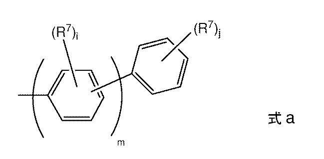
ある実施形態においては、式Iまたは式I’の化合物は、式Ia、すなわち、 In some embodiments, the compound of formula I or formula I 'is of formula Ia, i.e.
(ここで、R1〜R6、Ar1、Ar2、a〜h、およびnは式Iについて上に定義された通りである)
を有する。
(Where R 1 -R 6 , Ar 1 , Ar 2 , ah, and n are as defined above for Formula I)
Have
式Iまたは式I’のある実施形態においては、Ar1およびAr2は、縮合環を持たないアリール基である。ある実施形態においては、Ar1およびAr2は、式aを有し、 In some embodiments of Formula I or Formula I ′, Ar 1 and Ar 2 are aryl groups that have no fused rings. In some embodiments, Ar 1 and Ar 2 have the formula a
ここで:
R7は、それぞれの場合に同じもしくは異なるものであり、D、アルキル、アルコキシ、シロキサンおよびシリルからなる群から選択され;
iは、それぞれの場合に同じもしくは異なるものであり、0〜4の整数であり;
jは、0〜5の整数であり;
mは、1〜5の整数である。
here:
R 7 is the same or different in each case and is selected from the group consisting of D, alkyl, alkoxy, siloxane and silyl;
i is the same or different in each case and is an integer from 0 to 4;
j is an integer from 0 to 5;
m is an integer of 1-5.
ある実施形態においては、Ar1およびAr2は、式bを有し、 In some embodiments, Ar 1 and Ar 2 have the formula b:
ここで:
R7は、それぞれの場合に同じもしくは異なるものであり、D、アルキル、アルコキシ、シロキサンおよびシリルからなる群から選択され;
iは、それぞれの場合に同じもしくは異なるものであり、0〜4の整数であり;
jは、0〜5の整数であり;
mは、1〜5の整数である。
here:
R 7 is the same or different in each case and is selected from the group consisting of D, alkyl, alkoxy, siloxane and silyl;
i is the same or different in each case and is an integer from 0 to 4;
j is an integer from 0 to 5;
m is an integer of 1-5.
式aおよびbのある実施形態においては、iおよびjの少なくとも1つはゼロではない。ある実施形態においては、m=1〜3である。 In certain embodiments of Formulas a and b, at least one of i and j is not zero. In some embodiments, m = 1-3.
ある実施形態においては、Ar1およびAr2は、フェニル、ビフェニル、テルフェニル、それらの重水素化誘導体、ならびにアルキル、アルコキシ、シリル、および架橋基を持った置換基からなる群から選択される1つまたは複数の置換基を有するそれらの誘導体からなる群から選択される。 In some embodiments, Ar 1 and Ar 2 are selected from the group consisting of phenyl, biphenyl, terphenyl, deuterated derivatives thereof, and alkyl, alkoxy, silyl, and substituents with bridging groups. Selected from the group consisting of derivatives thereof having one or more substituents.
ある実施形態においては、R1〜R5はDまたはC1~10アルキルである。ある実施形態においては、アルキル基は重水素化されている。 In some embodiments, R 1 -R 5 are D or C 1-10 alkyl. In some embodiments, the alkyl group is deuterated.
ある実施形態においては、a=e=0である。ある実施形態においては、a=e=4であり、R1およびR5はDである。 In some embodiments, a = e = 0. In some embodiments, a = e = 4 and R 1 and R 5 are D.
ある実施形態においては、b>0であり、少なくとも1つのR2はアルキルである。ある実施形態においては、アルキル基は重水素化されている。ある実施形態においては、b=4であり、1つのR2はアルキルであり、残りはDである。 In certain embodiments, b> 0 and at least one R 2 is alkyl. In some embodiments, the alkyl group is deuterated. In some embodiments, b = 4, one R 2 is alkyl, and the remainder is D.
ある実施形態においては、c>0であり、少なくとも1つのR3はアルキルである。ある実施形態においては、アルキル基は重水素化されている。ある実施形態においては、c=4であり、1つのR3はアルキルであり、残りはDである。ある実施形態においては、c=4であり、2つのR3はアルキルであり、2つのR3はDである。 In certain embodiments, c> 0 and at least one R 3 is alkyl. In some embodiments, the alkyl group is deuterated. In some embodiments, c = 4, one R 3 is alkyl, and the remainder is D. In some embodiments, c = 4, two R 3 are alkyl, and two R 3 are D.
ある実施形態においては、d>0であり、少なくとも1つのR4はアルキルである。ある実施形態においては、このアルキル基は重水素化されている。ある実施形態においては、d=4であり、1つのR4はアルキルであり、残りはDである。 In certain embodiments, d> 0 and at least one R 4 is alkyl. In certain embodiments, the alkyl group is deuterated. In certain embodiments, d = 4, one R 4 is alkyl, and the remainder are D.
ある実施形態においては、f=h=2である。 In some embodiments, f = h = 2.
ある実施形態においては、g=1である。 In some embodiments, g = 1.
ある実施形態においては、式Iまたは式I’を有する化合物は、高い三重項エネルギーを有する。用語「三重項エネルギー」は、eV単位で、材料の最低励起三重項状態を意味する。三重項エネルギーは、正の数として報告され、基底状態、通常は一重項状態に対する三重項状態のエネルギーを表す。発光性有機金属材料は、混合一重項および三重項特性を有する励起状態から発光し、本明細書においては「リン光性」と言われる。有機金属のリン光性材料が発光層に使用される場合、低い三重項エネルギーを有する材料の存在は、2.0eV超のエネルギーのリン光性放射の消光をもたらす。これは、効率の低下につながる。消光は、ホスト材料などの、材料がエレクトロルミネセンス層中に、またはデバイスにおける他の層中に存在する場合に起こり得る。ある実施形態においては、式Iまたは式I’を有する材料は、2.1eVよりも大きい三重項エネルギーレベルを有し;ある実施形態においては、2.2eVよりも大きい;ある実施形態においては、2.45eVよりも大きい;ある実施形態においては、2.6eVよりも大きい三重項エネルギーレベルを有する。三重項エネルギーは、演繹的に計算することができるか、パルス放射線分解または低温ルミネセンス分光法を用いて測定することができるかのどちらかである。 In certain embodiments, the compound having Formula I or Formula I 'has a high triplet energy. The term “triplet energy” means the lowest excited triplet state of a material in eV. Triplet energy is reported as a positive number and represents the energy of the triplet state relative to the ground state, usually the singlet state. A luminescent organometallic material emits light from an excited state having mixed singlet and triplet properties and is referred to herein as “phosphorescent”. When an organometallic phosphorescent material is used for the emissive layer, the presence of a material with a low triplet energy results in quenching of phosphorescent radiation with energy above 2.0 eV. This leads to a decrease in efficiency. Quenching can occur when a material, such as a host material, is present in the electroluminescent layer or in other layers in the device. In some embodiments, the material having Formula I or Formula I ′ has a triplet energy level greater than 2.1 eV; in some embodiments, greater than 2.2 eV; Greater than 2.45 eV; in some embodiments, a triplet energy level greater than 2.6 eV. Triplet energy can either be calculated a priori or can be measured using pulse radiolysis or low temperature luminescence spectroscopy.
式Iまたは式I’を有する化合物の幾つかの非限定的な例としては、以下の化合物A〜EEが挙げられる。 Some non-limiting examples of compounds having Formula I or Formula I 'include the following compounds A-EE.
本新規化合物は、C−CまたはC−N結合を生成するであろう任意の技術を用いて製造することができる。Suzuki,Yamamoto,Stille,およびPd−またはNi−触媒C−Nカップリングなどの、様々なそのような技術は公知である。重水素化化合物は、重水素化前駆体材料を使用して類似の方法でまたは、より一般的には、非重水素化化合物を、三塩化アルミニウムもしくはエチルアルミニウムジクロリドなどの、ルイス酸H/D交換触媒の存在下に、d6−ベンゼンなどの、重水素化溶媒で処理することによって調製することができる。例示的な調製は、実施例において示される。 The novel compounds can be prepared using any technique that will generate a C—C or C—N bond. Various such techniques are known, such as Suzuki, Yamamoto, Stille, and Pd- or Ni-catalyzed CN coupling. Deuterated compounds are synthesized in a similar manner using deuterated precursor materials or, more commonly, non-deuterated compounds such as Lewis acid H / D, such as aluminum trichloride or ethylaluminum dichloride. It can be prepared by treatment with a deuterated solvent, such as d6-benzene, in the presence of an exchange catalyst. An exemplary preparation is shown in the examples.
本化合物は、溶液処理技術を用いて層を形成することができる。用語「層」は、用語「フィルム」と同じ意味で用いられ、所望の領域を覆うコーティングを意味する。この用語はサイズによって限定されない。この領域は、全体デバイスほどに大きいかもしくは実視覚表示などの特異的な機能領域ほどに小さい、または単一サブピクセルほどに小さいものであり得る。層およびフィルムは、蒸着、液相堆積(連続および不連続技術)、ならびに熱転写などの、任意の従来型堆積技術によって形成することができる。連続堆積技術としては、スピンコーティング、グラビアコーティング、カーテンコーティング、浸漬コーティング、スロット−ダイコーティング、スプレーコーティング、および連続ノズルコーティングが挙げられるが、これらに限定されるものではない。不連続堆積技術としては、インクジェット印刷、グラビア印刷、およびスクリーン印刷が挙げられるが、これらに限定されるものではない。 The compound can form layers using solution processing techniques. The term “layer” is used interchangeably with the term “film” and refers to a coating covering a desired area. This term is not limited by size. This area can be as large as the entire device or as small as a specific functional area such as a real visual display, or as small as a single sub-pixel. Layers and films can be formed by any conventional deposition technique, such as vapor deposition, liquid deposition (continuous and discontinuous techniques), and thermal transfer. Continuous deposition techniques include, but are not limited to, spin coating, gravure coating, curtain coating, dip coating, slot-die coating, spray coating, and continuous nozzle coating. Discontinuous deposition techniques include, but are not limited to, ink jet printing, gravure printing, and screen printing.
4.有機電子デバイス
本方法は、電子デバイスにおけるその適用の観点からさらに説明されるが、それはそのような適用に限定されない。
4). Organic Electronic Device Although the method is further described in terms of its application in electronic devices, it is not limited to such application.
図2は、2つの電気接触層の間に置かれた少なくとも2つの有機活性層を含む、例示的な電子デバイス、有機発光ダイオード(OLED)ディスプレイである。電子デバイス100は、アノード層110から放射層(emissive layer)140への正孔の注入を促進する1つまたは複数の層120および130を含む。一般に、2つの層が存在する場合、アノードに隣接した層120は正孔注入層と呼ばれ、緩衝層と呼ばれることもある。放射層に隣接した層130は正孔輸送層と呼ばれる。任意選択の電子輸送層150は、放射層140とカソード層160との間に置かれる。有機層120〜150は、個々におよびまとめてデバイスの有機活性層と言われる。デバイス100の用途に依存して、放射層140は、印加電圧によって活性化される発光層(発光ダイオードまたは発光電気化学セル中など)、放射エネルギーに応答し、そして印加バイアス電圧を使用してまたは使用せずに信号を発生する材料の層(光検出器中など)であり得る。このデバイスは、システム、駆動方法、および実用性モードに関して限定されない。下塗り層はこの図では示されていない。
FIG. 2 is an exemplary electronic device, an organic light emitting diode (OLED) display, comprising at least two organic active layers placed between two electrical contact layers. The
マルチカラーデバイスのためには、放射層140は、少なくとも3つの異なる色の異なる領域で構成される。異なる色の領域は、別個の着色領域を印刷することによって形成することができる。あるいは、それは、全体の層を形成し、そして層の異なる領域を異なる色の放射性材料でドープすることによって成し遂げることができる。そのような方法は、たとえば、米国特許出願公開第2004−0094768号明細書に記載されている。
For multicolor devices, the
ある実施形態においては、本明細書に記載される新規方法は、第2層が特定の領域に閉じ込められている、デバイスにおける任意の連続ペアの有機層のために用いることができる。第1有機活性層および第2有機活性層がその上に置かれた電極を含んでなる有機電子デバイスの製造方法は、
第1表面エネルギーを有する第1有機活性層を電極の上に形成する工程と;
第1有機活性層を下塗り材料で処理して下塗り層を形成する工程と;
下塗り層を放射線でパターン様に露光し、露光部と非露光部とをもたらす工程と;
下塗り層を展開して下塗り層を非露光部から除去し、下塗り層のパターンを有する第1活性有機層をもたらす工程であって、下塗り層のパターンが第1表面エネルギーよりも高い第2表面エネルギーを有する工程と;
第1有機活性層上の下塗り層のパターン上に液相堆積によって第2有機活性層を形成する工程と
を含んでなり、
ここで、下塗り材料は、上記のような、式Iまたは式I’を有する。
In certain embodiments, the novel methods described herein can be used for any continuous pair of organic layers in a device where the second layer is confined to a particular region. An organic electronic device manufacturing method comprising an electrode having a first organic active layer and a second organic active layer disposed thereon,
Forming a first organic active layer having a first surface energy on the electrode;
Treating the first organic active layer with an undercoat material to form an undercoat layer;
Exposing the subbing layer in a pattern-wise manner with radiation to provide exposed and non-exposed areas;
Developing the undercoat layer to remove the undercoat layer from the non-exposed area, resulting in a first active organic layer having a pattern of the undercoat layer, wherein the second surface energy is higher than the first surface energy. A process comprising:
Forming a second organic active layer by liquid deposition on a pattern of an undercoat layer on the first organic active layer,
Here, the primer material has the formula I or formula I ′ as described above.
本新規方法の一実施形態においては、第2有機活性層は放射層140であり、第1有機活性層は、層140の直前に適用されたデバイス層である。多くの場合にデバイスは、アノードで始まって構築される。正孔輸送層130が存在する場合には、下塗り層は層130に適用され、放射層140を適用する前に展開されるであろう。層130が存在しない場合には、下塗り層は層120に適用されるであろう。デバイスがカソードで始まって構築される場合には、下塗り層は、放射層140を適用する前に電子輸送層150に適用されるであろう。
In one embodiment of the novel method, the second organic active layer is the
本新規方法の一実施形態においては、第1有機活性層は正孔注入層120であり、第2有機活性層は正孔輸送層130である。デバイスがアノード層で始まって構築される実施形態においては、下塗り層は正孔注入層120に適用され、正孔輸送層130を適用する前に展開される。一実施形態においては、正孔注入層は、フッ素化材料を含んでなる。一実施形態においては、正孔注入層は、フッ素化酸ポリマーでドープされた導電性ポリマーを含んでなる。一実施形態においては、正孔注入層は本質的に、フッ素化酸ポリマーでドープされた導電性ポリマーからなる。ある実施形態においては、下塗り層は本質的に、正孔輸送材料からなる。一実施形態においては、下塗り層は本質的に、正孔輸送層と同じ正孔輸送材料からなる。
In one embodiment of the novel method, the first organic active layer is a
デバイスにおけるこれらの層は、そのような層に有用であることが知られている任意の材料製であり得る。本発明のデバイスは、アノード層110またはカソード層160に隣接することができる支持体または基材(図示せず)を含んでもよい。ほとんどの場合に、支持体はアノード層110に隣接している。支持体は、可撓性であることも剛性であることも、有機であることも無機であることもできる。一般に、ガラスまたは可撓性有機フィルムが支持体として使用される。アノード層110は、カソード層160と比較して正孔を注入するためにより効率的である電極である。アノードは、金属、混合金属、合金、金属酸化物または混合酸化物を含有する材料を含むことができる。好適な材料としては、2族元素(すなわち、Be、Mg、Ca、Sr、Ba)の混合酸化物、11族元素、4族、5族、および6族の元素、ならびに8〜10族の遷移元素が挙げられる。アノード層110が光透過性であるべきである場合には、インジウム・スズ酸化物などの12族、13族、および14族の元素の混合酸化物を使用することができる。本明細書において使用される場合、語句「混合酸化物」は、2族元素または12族、13族、または14族の元素から選択される2つ以上の異なる陽イオンを有する酸化物を意味する。アノード層110用の材料の幾つかの非限定的な具体例としては、インジウム・スズ酸化物(「ITO」)、アルミニウム・スズ酸化物、アルミニウム・亜鉛酸化物、金、銀、銅、およびニッケルが挙げられるが、これらに限定されるものではない。アノードはまた、ポリアニリン、ポリチオフェン、またはポリピロールなどの有機材料を含んでなることができる。
These layers in the device can be made of any material known to be useful for such layers. The device of the present invention may include a support or substrate (not shown) that can be adjacent to the
アノード層110は、化学蒸着法もしくは物理蒸着法またはスピンキャスト法によって形成することができる。化学蒸着は、プラズマ化学蒸着(「PECVD」)または金属有機化学蒸着(「MOCVD」)として行うことができる。物理蒸着としては、イオンビームスパッタリングなどのスパッタリング、ならびにeビーム蒸発および抵抗蒸発の任意の形態を挙げることができる。物理蒸着の具体的な形態としては、rfマグネトロンスパッタリングおよび誘導結合プラズマ物理蒸着(「IMP−PVD」)が挙げられる。これらの堆積技術は、半導体製造分野においては周知である。
The
通常、アノード層110は、リソグラフ操作中にパターン化される。このパターンは、要望通りに変わってもよい。これらの層は、たとえば、パターン化マスクまたはレジストを、第1電気接触層材料を適用する前に第1可撓性複合材料バリア構造上に置くことによってパターンで形成することができる。あるいは、これらの層は、全体の層として適用することができ(ブランケット堆積とも呼ばれる)、続いて、たとえば、パターン化されたレジスト層と湿式化学エッチングまたはドライエッチング技術とを使用してパターン化することができる。当技術分野において周知である他のパターン化方法を使用することもできる。電子デバイスが配列内に置かれる場合、アノード層110は典型的には、実質的に同じ方向に伸びる長さを有する実質的に平行のストリップに成形される。
Usually, the
正孔注入層120は、放射層への正孔の注入を促進する、およびアノード表面を平坦化してデバイスにおけるショートを防ぐ機能を果たす。正孔注入材料は、ポリマー、オリゴマー、または小分子であってもよく、溶液、分散液、懸濁液、エマルジョン、コロイド状混合物、またはその他の組成物の形態にあってもよい。
The
正孔注入層は、多くの場合プロトン酸でドープされている、ポリアニリン(PANI)またはポリエチレンジオキシチオフェン(PEDOT)などの、ポリマー材料で形成することができる。これらのプロトン酸は、たとえば、ポリ(スチレンスルホン酸)、ポリ(2−アクリルアミド−2−メチル−1−プロパンスルホン酸)などであり得る。正孔注入層120は、銅フタロシアニンおよびテトラチアフルバレン−テトラシアノキノジメタン系(TTF−TCNQ)などの、電荷移動化合物などを含んでなることができる。一実施形態においては、正孔注入層120は、導電性ポリマーおよびコロイド形成性ポリマー酸の分散液から製造される。そのような材料は、たとえば、米国特許出願公開第2004/0102577号明細書、同第2004/0127637号明細書、同第2005/0205860号明細書、および国際公開第2009/018009号パンフレットに記載されている。
The hole injection layer can be formed of a polymeric material, such as polyaniline (PANI) or polyethylenedioxythiophene (PEDOT), often doped with a protonic acid. These protonic acids can be, for example, poly (styrene sulfonic acid), poly (2-acrylamido-2-methyl-1-propanesulfonic acid), and the like. The
正孔注入層120は、任意の堆積技術によって適用することができる。一実施形態においては、正孔注入層は、上に記載されたような、溶液堆積法によって適用される。一実施形態においては、正孔注入層は、連続溶液堆積法によって適用される。
The
層130は、正孔輸送材料を含んでなる。正孔輸送層用の正孔輸送材料の例は、たとえば、Y.Wang,Kirk−Othmer Encyclopedia of Chemical Technology,Fourth Edition,Vol.18,p.837−860,1996にまとめられている。正孔輸送小分子および正孔輸送ポリマーの両方を使用することができる。一般に使用される正孔輸送分子としては:4,4’,4’’−トリス(N,N−ジフェニル−アミノ)−トリフェニルアミン(TDATA);4,4’,4’’−トリス(N−3−メチルフェニル−N−フェニル−アミノ)−トリフェニルアミン(MTDATA);N,N’−ジフェニル−N,N’−ビス(3−メチルフェニル)−[1,1’−ビフェニル]−4,4’−ジアミン(TPD);4、4’−ビス(カルバゾール−9−イル)ビフェニル(CBP);1,3−ビス(カルバゾール−9−イル)ベンゼン(mCP);1,1−ビス[(ジ−4−トリルアミノ)フェニル]シクロヘキサン(TAPC);N,N’−ビス(4−メチルフェニル)−N,N’−ビス(4−エチルフェニル)−[1,1’−(3,3’−ジメチル)ビフェニル]−4,4’−ジアミン(ETPD);テトラキス−(3−メチルフェニル)−N,N,N’,N’−2,5−フェニレンジアミン(PDA);α−フェニル−4−N,N−ジフェニルアミノスチレン(TPS);p−(ジエチルアミノ)ベンズアルデヒドジフェニルヒドラゾン(DEH);トリフェニルアミン(TPA);ビス[4−(N,N−ジエチルアミノ)−2−メチルフェニル](4−メチルフェニル)メタン(MPMP);1−フェニル−3−[p−(ジエチルアミノ)スチリル]−5−[p−(ジエチルアミノ)フェニル]ピラゾリン(PPRまたはDEASP);1,2−トランス−ビス(9H−カルバゾール−9−イル)シクロブタン(DCZB);N,N,N’,N’−テトラキス(4−メチルフェニル)−(1,1’−ビフェニル)−4,4’−ジアミン(TTB);N,N’−ビス(ナフタレン−1−イル)−N,N’−ビス(フェニル)ベンジジン(α−NPB);および、銅フタロシアニンなどの、ポルフィリン化合物が挙げられるが、これらに限定されるものではない。一般に使用される正孔輸送ポリマーとしては、ポリビニルカルバゾール、(フェニルメチル)ポリシラン、ポリ(ジオキシチオフェン)、ポリアニリン、およびポリピロールが挙げられるが、これらに限定されるものではない。上述のものなどの正孔輸送分子をポリスチレンおよびポリカーボネートなどのポリマーへドープすることによって正孔輸送ポリマーを得ることもまた可能である。
ある実施形態においては、正孔輸送層は正孔輸送ポリマーを含んでなる。ある実施形態においては、正孔輸送層は本質的に、正孔輸送ポリマーからなる。ある実施形態においては、正孔輸送ポリマーはジスチリルアリール化合物である。ある実施形態においては、このアリール基は2つ以上の縮合芳香環を有するものである。ある実施形態においては、このアリール基はアセンである。用語「アセン」は、本明細書において使用される場合、2つ以上のオルト縮合ベンゼン環を真っ直ぐの線状配置で含有する炭化水素親成分を意味する。 In some embodiments, the hole transport layer comprises a hole transport polymer. In some embodiments, the hole transport layer consists essentially of a hole transport polymer. In some embodiments, the hole transport polymer is a distyrylaryl compound. In some embodiments, the aryl group has two or more fused aromatic rings. In certain embodiments, the aryl group is acene. The term “acene” as used herein refers to a hydrocarbon parent component that contains two or more ortho-fused benzene rings in a straight linear configuration.
ある実施形態においては、正孔輸送ポリマーはアリールアミンポリマーである。ある実施形態においては、それは、フルオレンモノマーとアリールアミンモノマーとのコポリマーである。 In some embodiments, the hole transport polymer is an arylamine polymer. In some embodiments, it is a copolymer of fluorene monomer and arylamine monomer.
ある実施形態においては、このポリマーは架橋性基を有する。ある実施形態においては、架橋は、熱処理および/またはUV線もしくは可視光への露光によって成し遂げることができる。架橋性基の例としては、ビニル、アクリレート、パーフルオロビニルエーテル、1−ベンゾ−3,4−シクロブタン、シロキサン、およびメチルエステルが挙げられるが、これらに限定されるものではない。架橋性ポリマーは、溶液法OLEDの製造において利点を有することができる。堆積の後に不溶性フィルムへ変換することができる層を形成するための可溶性ポリマー材料の適用は、層溶解問題なしの多層溶液処理OLEDデバイスの製造を可能にすることができる。 In some embodiments, the polymer has crosslinkable groups. In some embodiments, crosslinking can be accomplished by heat treatment and / or exposure to UV radiation or visible light. Examples of crosslinkable groups include, but are not limited to, vinyl, acrylate, perfluorovinyl ether, 1-benzo-3,4-cyclobutane, siloxane, and methyl ester. Crosslinkable polymers can have advantages in the production of solution process OLEDs. Application of a soluble polymeric material to form a layer that can be converted to an insoluble film after deposition can allow for the production of multilayer solution processed OLED devices without layer dissolution problems.
架橋性ポリマーの例は、たとえば、米国特許出願公開第2005/0184287号明細書および国際公開第2005/052027号パンフレットに見いだすことができる。 Examples of crosslinkable polymers can be found, for example, in US 2005/0184287 and WO 2005/052027.
ある実施形態においては、正孔輸送層は、9,9−ジアルキルフルオレンとトリフェニルアミンとのコポリマーであるポリマーを含んでなる。ある実施形態においては、正孔輸送層は本質的に、9,9−ジアルキルフルオレンとトリフェニルアミンとのコポリマーであるポリマーからなる。ある実施形態においては、このポリマーは、9,9−ジアルキルフルオレンと4,4’−ビス(ジフェニルアミノ)ビフェニルとのコポリマーである。ある実施形態においては、このポリマーは、9,9−ジアルキルフルオレンとTPBとのコポリマーである。ある実施形態においては、このポリマーは、9,9−ジアルキルフルオレンとNPBとのコポリマーである。ある実施形態においては、このコポリマーは、(ビニルフェニル)ジフェニルアミンおよび9,9−ジスチリルフルオレンまたは9,9−ジ(ビニルベンジル)フルオレンから選択される第3コモノマーから製造される。ある実施形態においては、正孔輸送層は、非平面立体配置で連結されている共役部分を有するトリアリールアミンを含んでなる材料を含んでなる。そのような材料は、モノマーまたはポリマーであり得る。そのような材料の例は、たとえば、国際公開第2009/067419号パンフレットに記載されている。 In some embodiments, the hole transport layer comprises a polymer that is a copolymer of 9,9-dialkylfluorene and triphenylamine. In some embodiments, the hole transport layer consists essentially of a polymer that is a copolymer of 9,9-dialkylfluorene and triphenylamine. In some embodiments, the polymer is a copolymer of 9,9-dialkylfluorene and 4,4'-bis (diphenylamino) biphenyl. In some embodiments, the polymer is a copolymer of 9,9-dialkylfluorene and TPB. In some embodiments, the polymer is a copolymer of 9,9-dialkylfluorene and NPB. In some embodiments, the copolymer is made from a third comonomer selected from (vinylphenyl) diphenylamine and 9,9-distyrylfluorene or 9,9-di (vinylbenzyl) fluorene. In some embodiments, the hole transport layer comprises a material comprising a triarylamine having conjugated moieties connected in a non-planar configuration. Such materials can be monomers or polymers. Examples of such materials are described, for example, in WO 2009/067419.
ある実施形態においては、正孔輸送層は、テトラフルオロテトラシアノキノジメタンおよびペリレン−3,4,9,10−テトラカルボン酸−3,4,9,10二無水物などの、p−ドーパントでドープされている。 In some embodiments, the hole transport layer is a p-dopant, such as tetrafluorotetracyanoquinodimethane and perylene-3,4,9,10-tetracarboxylic acid-3,4,9,10 dianhydride. It is doped with.
ある実施形態においては、正孔輸送層は、上に記載されたような、式Iまたは式I’を有する材料を含んでなる。ある実施形態においては、正孔輸送層は本質的に、式Iまたは式I’を有する材料からなる。 In some embodiments, the hole transport layer comprises a material having Formula I or Formula I ', as described above. In some embodiments, the hole transport layer consists essentially of a material having Formula I or Formula I '.
正孔輸送層130は、任意の堆積技術によって適用することができる。一実施形態においては、正孔輸送層は、上に記載されたような、溶液堆積法によって適用される。一実施形態においては、正孔輸送層は、連続溶液堆積法によって適用される。
The
デバイスの用途に依存して、放射層140は、印加電圧によって活性化される発光層(発光ダイオードまたは発光電気化学セル中など)、放射エネルギーに応答し、そして印加バイアス電圧を使用してまたは使用せずに信号を発生する材料の層(光検出器中など)であり得る。一実施形態においては、放射性材料は、有機エレクトロルミネセンス(「EL」)材料である。小分子有機蛍光性化合物、蛍光性およびリン光性の金属錯体、共役ポリマー、およびそれらの混合物を含むが、これらに限定されない、任意のEL材料を本発明のデバイスに使用することができる。蛍光性化合物の例としては、クリセン、ピレン、ペリレン、ルブレン、クマリン、アントラセン、チアジアゾール、それらの誘導体、およびそれらの混合物が挙げられるが、これらに限定されるものではない。金属錯体の例としては、トリス(8−ヒドロキシキノラト)アルミニウム(Alq3)などの、金属キレート化オキシノイド化合物;Petrovらの米国特許第6,670,645号明細書ならびに国際公開第03/063555号パンフレットおよび国際公開第2004/016710号パンフレットに開示されているようなフェニルピリジン配位子、フェニルキノリン配位子、またはフェニルピリミジン配位子を有するイリジウムの錯体などの、シクロメタレート化イリジウムおよび白金エレクトロルミネッセンス化合物、ならびに、たとえば、国際公開第03/008424号パンフレット、国際公開第03/091688号パンフレット、および国際公開第03/040257号パンフレットに記載されている有機金属錯体、ならびにそれらの混合物が挙げられるが、これらに限定されるものではない。ある場合には、小分子蛍光性材料または有機金属材料が、加工特性および/または電子特性を向上させるためにホスト材料とともにドーパントとして堆積される。共役ポリマーの例としては、ポリ(フェニレンビニレン)、ポリフルオレン、ポリ(スピロビフルオレン)、ポリチオフェン、ポリ(p−フェニレン)、それらのコポリマー、およびそれらの混合物が挙げられるが、これらに限定されるものではない。
Depending on the device application, the
放射層140は、任意の堆積技術によって適用することができる。一実施形態においては、放射層は、上に記載されたような、溶液堆積法によって適用される。一実施形態においては、放射層は、連続溶液堆積法によって適用される。
The
任意選択の層150は、電子輸送を促進する、およびまた緩衝層または層界面での励起子の消光を防止するための閉じ込め層として役立つという両方の機能を果たすことができる。好ましくは、この層は、電子の移動を促進し、かつ、励起子の消光を減少させる。任意選択の電子輸送層150に使用することができる電子輸送材料の例としては、トリス(8−ヒドロキシキノラト)アルミニウム(AlQ)、ビス(2−メチル−8−キノリノラト)(p−フェニルフェノラト)アルミニウム(BAlq)、テトラキス−(8−ヒドロキシキノラト)ハフニウム(HfQ)およびテトラキス−(8−ヒドロキシキノラト)ジルコニウム(ZrQ)などの金属キノレート誘導体などの、金属キレート化オキシノイド化合物;ならびに2−(4−ビフェニリル)−5−(4−t−ブチルフェニル)−1,3,4−オキサジアゾール(PBD)、3−(4−ビフェニリル)−4−フェニル−5−(4−t−ブチルフェニル)−1,2,4−トリアゾール(TAZ)、および1,3,5−トリ(フェニル−2−ベンズイミダゾール)ベンゼン(TPBI)などのアゾール化合物;2,3−ビス(4−フルオロフェニル)キノキサリンなどのキノキサリン誘導体;4,7−ジフェニル−1,10−フェナントロリン(DPA)および2,9−ジメチル−4,7−ジフェニル−1,10−フェナントロリン(DDPA)などのフェナントロリン類;ならびにそれらの混合物が挙げられる。ある実施形態においては、電子輸送層は、n−ドーパントをさらに含んでなる。n−ドーパント材料は周知である。n−ドーパントとしては、1族および2族金属;LiF、CsF、およびCs2CO3などの、1族および2族金属塩;Liキノレートなどの、1族および2族金属有機化合物;ならびにロイコ染料などの、分子n−ドーパント、W2(hpp)4(ここで、hpp=1,3,4,6,7,8−ヘキサヒドロ−2H−ピリミド−[1,2−a]−ピリミジンである)およびコバルトセンなどの、金属錯体、テトラチアナフタセン、ビス(エチレンジチオ)テトラチアフルバレン、複素環ラジカルまたはジラジカル、ならびに複素環ラジカルまたはジラジカルのダイマー、オリゴマー、ポリマー、ジスピロ化合物および多環化合物などが挙げられるが、これらに限定されるものではない。
電子輸送層150は通常、化学蒸着法または物理蒸着法によって形成される。
The
カソード160は、電子または負電荷キャリアを注入するために特に有効である電極である。カソードは、アノードよりも低い仕事関数を有する任意の金属または非金属であり得る。カソード用の材料は、1族のアルカリ金属(たとえば、Li、Cs)、2族(アルカリ土類)金属、希土類元素およびランタニドなどの、12族金属、およびアクチニドから選択することができる。アルミニウム、インジウム、カルシウム、バリウム、サマリウムおよびマグネシウム、ならびに組み合わせなどの材料を使用することができる。Li含有有機金属化合物、LiF、Li2O、Cs含有有機金属化合物、CsF、Cs2O、およびCs2CO3をまた、作動電圧を低くするためにカソード層の堆積の前に堆積することができる。この層は電子注入層と言われてもよい。
The
カソード層160は通常、化学蒸着法または物理蒸着法によって形成される。
The
ある実施形態においては、追加の層が有機電子デバイス内に存在してもよい。 In some embodiments, additional layers may be present in the organic electronic device.
各機能性層を2つ以上の層で構成できることは理解される。 It is understood that each functional layer can be composed of more than one layer.
一実施形態においては、異なる層は以下の範囲の厚さを有する:アノード110、100〜5000Å、一実施形態においては100〜2000Å;正孔注入層120、50〜2500Å、一実施形態においては200〜1000Å;正孔輸送層130、50〜2500Å、一実施形態においては200〜1000Å;放射層140、10〜2000Å、一実施形態においては100〜1000Å;電子輸送層150、50〜2000Å、一実施形態においては100〜1000Å;カソード160、200〜10000Å、一実施形態においては300〜5000Å。電子注入層が存在する場合、堆積される材料の量は一般に、1〜100Å、一実施形態においては1〜10Åの範囲にある。層の厚さの望ましい比は、使用される材料の厳密な性質に依存する。
In one embodiment, the different layers have thicknesses in the following ranges:
ある実施形態においては、電極の上に置かれた第1有機活性層および第2有機活性層を含んでなり、そして第1有機活性層と第2有機活性層との間にパターン化下塗り層をさらに含んでなる有機電子デバイスであって、前記第2有機活性層が、下塗り層が存在する領域のみに存在し、かつ、下塗り層が、上に記載されたような、式Iまたは式I’を有する材料を含んでなるデバイスが提供される。ある実施形態においては、下塗り層は本質的に、式Iまたは式I’を有する材料からなる。ある実施形態においては、第1有機活性層は、導電性ポリマーおよびフッ素化酸ポリマーを含んでなる。ある実施形態においては、第2有機活性層は、正孔輸送材料を含んでなる。ある実施形態においては、第1有機活性層は、フッ素化酸ポリマーでドープされた導電性ポリマーを含んでなり、第2有機活性層は本質的に、正孔輸送材料からなる。 In some embodiments, a first organic active layer and a second organic active layer disposed on the electrode, and a patterned subbing layer between the first organic active layer and the second organic active layer. Further comprising an organic electronic device, wherein the second organic active layer is present only in the region where the subbing layer is present and the subbing layer is as described above, formula I or formula I ′ There is provided a device comprising a material having: In some embodiments, the subbing layer consists essentially of a material having Formula I or Formula I '. In some embodiments, the first organic active layer comprises a conductive polymer and a fluorinated acid polymer. In some embodiments, the second organic active layer comprises a hole transport material. In some embodiments, the first organic active layer comprises a conductive polymer doped with a fluorinated acid polymer, and the second organic active layer consists essentially of a hole transport material.
ある実施形態においては、正孔注入層および正孔輸送層をその上に有するアノードを含んでなる有機電子デバイスの製造方法であって、前記方法が、
アノードの上に正孔注入層を形成する工程であって、前記正孔注入層がフッ素化材料を含んでなり、第1表面エネルギーを有する工程と;
下塗り層を正孔注入層上に直接形成する工程と;
下塗り層を放射線でパターン様に露光し、露光部と非露光部とをもたらす工程と;
下塗り層を展開して下塗り層を非露光部から効果的に除去し、展開された下塗り層のパターンを正孔注入層上にもたらす工程であって、前記展開された下塗り層が第1表面エネルギーより高い第2表面エネルギーを有する工程と;
下塗り層の展開されたパターン上に液相堆積によって正孔輸送層を形成する工程と
を含んでなり、
ここで、下塗り層が、上記のような、式Iまたは式I’を有する材料を含んでなる
方法が提供される。
In one embodiment, a method for producing an organic electronic device comprising an anode having a hole injection layer and a hole transport layer thereon, the method comprising:
Forming a hole injection layer on the anode, the hole injection layer comprising a fluorinated material and having a first surface energy;
Forming an undercoat layer directly on the hole injection layer;
Exposing the subbing layer in a pattern-wise manner with radiation to provide exposed and non-exposed areas;
Developing the undercoat layer to effectively remove the undercoat layer from the non-exposed portion, and providing the developed undercoat layer pattern on the hole injection layer, wherein the developed undercoat layer has a first surface energy. Having a higher second surface energy;
Forming a hole transport layer by liquid phase deposition on the developed pattern of the undercoat layer,
Here, a method is provided wherein the subbing layer comprises a material having Formula I or Formula I ′ as described above.
これは、図3に概略的に示される。デバイス200は、基材(図示せず)上にアノード210を有する。アノード上に正孔注入層220がある。展開された下塗り層は225として示される。正孔注入層220の表面エネルギーは、下塗り層225の表面エネルギーよりも小さい。正孔輸送層230が下塗り層および正孔注入層の上に堆積される場合、それは、正孔注入層の低エネルギー表面をぬらさず、下塗り層のパターンの上にのみ残る。
This is shown schematically in FIG.
ある実施形態においては、正孔注入層は、フッ素化酸ポリマーでドープされた導電性ポリマーを含んでなる。ある実施形態においては、正孔注入層は本質的に、フッ素化酸ポリマーでドープされた導電性ポリマーからなる。ある実施形態においては、正孔注入層は本質的に、フッ素化酸ポリマーでドープされた導電性ポリマーおよび無機ナノ粒子からなる。ある実施形態においては、これらの無機ナノ粒子は、酸化ケイ素、酸化チタン、酸化ジルコニウム、三酸化モリブデン、酸化バナジウム、酸化アルミニウム、酸化亜鉛、酸化サマリウム、酸化イットリウム、酸化セシウム、酸化第二銅、酸化第二スズ、酸化アンチモン、およびそれらの組み合わせからなる群から選択される。そのような材料は、たとえば、米国特許出願公開第2004/0102577号明細書、同第2004/0127637号明細書、同第2005/0205860号明細書、および国際公開第2009/018009号パンフレットに記載されている。 In some embodiments, the hole injection layer comprises a conductive polymer doped with a fluorinated acid polymer. In some embodiments, the hole injection layer consists essentially of a conductive polymer doped with a fluorinated acid polymer. In some embodiments, the hole injection layer consists essentially of a conductive polymer and inorganic nanoparticles doped with a fluorinated acid polymer. In some embodiments, these inorganic nanoparticles comprise silicon oxide, titanium oxide, zirconium oxide, molybdenum trioxide, vanadium oxide, aluminum oxide, zinc oxide, samarium oxide, yttrium oxide, cesium oxide, cupric oxide, oxidized Selected from the group consisting of stannic, antimony oxide, and combinations thereof. Such materials are described, for example, in U.S. Patent Application Publication Nos. 2004/0102577, 2004/0127637, 2005/0205860, and WO 2009/018009. ing.
ある実施形態においては、下塗り層は本質的に、式Iまたは式I’を有する材料からなる。 In some embodiments, the subbing layer consists essentially of a material having Formula I or Formula I '.
ある実施形態においては、正孔輸送層は、トリアリールアミン、カルバゾール類、それらのポリマー類似体、およびそれらの組み合わせからなる群から選択される。ある実施形態においては、正孔輸送層は、ポリマートリアリールアミン、非平面立体配置で連結されている共役部分を有するポリマートリアリールアミン、およびフルオレンとトリアリールアミンとのコポリマーからなる群から選択される。 In some embodiments, the hole transport layer is selected from the group consisting of triarylamines, carbazoles, polymer analogs thereof, and combinations thereof. In some embodiments, the hole transport layer is selected from the group consisting of polymeric triarylamines, polymeric triarylamines having conjugated moieties linked in a non-planar configuration, and copolymers of fluorene and triarylamine. The
ある実施形態においては、本方法は、正孔輸送層上に液相堆積によって放射層を形成する工程をさらに含んでなる。ある実施形態においては、この放射層は、エレクトロルミネセンスドーパントおよび1つまたは複数のホスト材料を含んでなる。ある実施形態においては、この放射層は、インクジェット印刷および連続ノズル印刷からなる群から選択される液相堆積技術によって形成される。 In some embodiments, the method further comprises the step of forming the emissive layer by liquid deposition on the hole transport layer. In certain embodiments, the emissive layer comprises an electroluminescent dopant and one or more host materials. In some embodiments, the emissive layer is formed by a liquid deposition technique selected from the group consisting of inkjet printing and continuous nozzle printing.
本明細書に記載される概念は、特許請求の範囲に記載される本発明の範囲を限定しない、以下の実施例でさらに説明される。 The concepts described herein are further illustrated in the following examples, which do not limit the scope of the invention described in the claims.
追加の原材料としては:
導電性ポリマーおよびポリマーフッ素化スルホン酸の水性分散液である、HIJ−1が挙げられる。そのような原材料は、たとえば、米国特許出願公開第2004/0102577号明細書、同第2004/0127637号明細書、同第2005/0205860号明細書、および国際公開第2009/018009号パンフレットに記載されている。
Additional raw materials include:
HIJ-1, which is an aqueous dispersion of a conductive polymer and a polymer fluorinated sulfonic acid. Such raw materials are described, for example, in U.S. Patent Application Publication Nos. 2004/0102577, 2004/0127637, 2005/0205860, and WO 2009/018009. ing.
合成実施例
本実施例は、化合物Rの合成を例示する。
Synthetic Examples This example illustrates the synthesis of Compound R.
1,4−ジブロモ−2,5−ジヘキシルベンゼン(8.05ミリモル、3.255g)、ホウ酸エステル26(17.7ミリモル、7.545g)、Na2CO3(40.3ミリモル、4.268g)およびAliquat 336(0.500g)を、撹拌棒および冷却器付きの250mLの2口丸底フラスコ中でトルエン(100mL)に懸濁させた。反応混合物を脱気し、Pd(PPh3)4(0.403ミリモル、0.465g)を加え、これに脱気水(50mL)の添加が続いた。反応物を90℃に2日間加熱した。生じた反応混合物を酢酸エチル(150mL)で希釈し、酢酸エチル(3×100mL)で洗浄した。有機層をブライン(2×100mL)で洗浄し、硫酸マグネシウム上で乾燥させ、濾過し、濃縮した。1:3DCM:ヘキサンを使用するシリカゲルでのカラムクロマトグラフィーによる精製は、白色粉末(56%、3.8g)を生成した。1H NMR(500MHz,CD2Cl2)δ=7.45(d,J=8.5Hz,4H),7.33−7.31(m,5H),7.26−7.19(m,5H),6.65(s,2H),2.71−2.63(m,9H0,1.54(s,18H),1.31−1.20(m,14H),1.15(t,J=7.49,7H),0.83(t,J=6.85Hz,6H)。 1,4-dibromo-2,5-dihexylbenzene (8.05 mmol, 3.255 g), borate ester 26 (17.7 mmol, 7.545 g), Na 2 CO 3 (40.3 mmol, 4.255 mmol). 268 g) and Aliquat 336 (0.500 g) were suspended in toluene (100 mL) in a 250 mL 2-neck round bottom flask with stir bar and condenser. The reaction mixture was degassed and Pd (PPh 3 ) 4 (0.403 mmol, 0.465 g) was added followed by the addition of degassed water (50 mL). The reaction was heated to 90 ° C. for 2 days. The resulting reaction mixture was diluted with ethyl acetate (150 mL) and washed with ethyl acetate (3 × 100 mL). The organic layer was washed with brine (2 × 100 mL), dried over magnesium sulfate, filtered and concentrated. Purification by column chromatography on silica gel using 1: 3 DCM: hexane yielded a white powder (56%, 3.8 g). 1 H NMR (500 MHz, CD 2 Cl 2 ) δ = 7.45 (d, J = 8.5 Hz, 4H), 7.33-7.31 (m, 5H), 7.26-7.19 (m , 5H), 6.65 (s, 2H), 2.71-2.63 (m, 9H0, 1.54 (s, 18H), 1.31-1.20 (m, 14H), 1.15. (T, J = 7.49, 7H), 0.83 (t, J = 6.85 Hz, 6H).
化合物27(4.54ミリモル、3.800g)を200mLの丸底フラスコに加え、ジクロロメタン(90mL)に溶解させた。トリフルオロ酢酸(45.4ミリモル、5.175g)をこの溶液に滴加した。1日後にジクロロメタンを回転蒸発によって除去し、生じた灰色粉末をエチルエーテル(100mL)に溶解させた。重炭酸ナトリウム(100mL)を加えてTFAを中和した。層を分離し、有機層を水(2×100mL)、続いて、ブライン(2×100mL)で洗浄した。硫酸マグネシウム上での乾燥および濃縮は、わずかに灰色がかった白い粉末(100%、2.891g)を生成した。1H NMR(500MHz,CD2Cl2)δ=7.28(m,2H),7.23−7.18(m,6H),7.16(d,J=8.47Hz,4H),6.76(d,J=8.37Hz,4H),3.77(s,4H),2.71−2.63(m,6H),1.3−1.19(m,16H),1.15(t,J=7.5Hz,8H),0.83(t,J=6.86Hz,6H)。 Compound 27 (4.54 mmol, 3.800 g) was added to a 200 mL round bottom flask and dissolved in dichloromethane (90 mL). Trifluoroacetic acid (45.4 mmol, 5.175 g) was added dropwise to this solution. After 1 day, the dichloromethane was removed by rotary evaporation and the resulting gray powder was dissolved in ethyl ether (100 mL). Sodium bicarbonate (100 mL) was added to neutralize TFA. The layers were separated and the organic layer was washed with water (2 × 100 mL) followed by brine (2 × 100 mL). Drying and concentration over magnesium sulfate produced a slightly off-white powder (100%, 2.891 g). 1 H NMR (500 MHz, CD 2 Cl 2 ) δ = 7.28 (m, 2H), 7.23-7.18 (m, 6H), 7.16 (d, J = 8.47 Hz, 4H), 6.76 (d, J = 8.37 Hz, 4H), 3.77 (s, 4H), 2.71-2.63 (m, 6H), 1.3-1.19 (m, 16H), 1.15 (t, J = 7.5 Hz, 8H), 0.83 (t, J = 6.86 Hz, 6H).
250mLの丸底フラスコに、ジアミン28(4.539ミリモル、2.891g)、ブロモビフェニル(9.123ミリモル、2.127g)およびトルエン(65mL)を加えた。続いて、Pd2(dba)3(0.227ミリモル、0.208g)およびPtBu3(0.454ミリモル、0.092g)を加えた。反応混合物を、塩基、NaOtBu(9.078ミリモル、0.845g)を加える前に5分間撹拌した。3日後に生じた反応混合物をトルエン(100mL)で希釈し、シリカおよびセライトのパッドを通して濾過し、トルエン(3×100mL)、続いて、酢酸エチル(2×100mL)で洗浄し、濃縮して茶色固体にした。溶出液1:6の酢酸エチル:ヘキサンを使用する、シリカゲルでのカラムクロマトグラフィーによる精製は、白色粉末(55%、2.367g)を生成した。1H NMR(500MHz,CD2Cl2)δ=7.61(d,J=7.24Hz,4H),7.57(d,J=8.51Hz,4H),7.43(t,J=7.6Hz,4H),7.34−7.28(m,12H),5.99(s,2H),2.73(q,J=Hz,4H),2.66(t,J=7.7Hz,6H),1.33−1.17(m,20H),0.84(t,J=7.2Hz,6H)。 To a 250 mL round bottom flask was added diamine 28 (4.539 mmol, 2.891 g), bromobiphenyl (9.123 mmol, 2.127 g) and toluene (65 mL). Subsequently, Pd 2 (dba) 3 (0.227 mmol, 0.208 g) and P t Bu3 (0.454 mmol, 0.092 g) were added. The reaction mixture was stirred for 5 minutes before adding the base, NaO t Bu (9.078 mmol, 0.845 g). The reaction mixture resulting after 3 days was diluted with toluene (100 mL), filtered through a pad of silica and celite, washed with toluene (3 × 100 mL) followed by ethyl acetate (2 × 100 mL) and concentrated to brown Solid. Purification by column chromatography on silica gel using eluent 1: 6 ethyl acetate: hexanes produced a white powder (55%, 2.367 g). 1 H NMR (500 MHz, CD 2 Cl 2 ) δ = 7.61 (d, J = 7.24 Hz, 4H), 7.57 (d, J = 8.51 Hz, 4H), 7.43 (t, J = 7.6 Hz, 4H), 7.34-7.28 (m, 12H), 5.99 (s, 2H), 2.73 (q, J = Hz, 4H), 2.66 (t, J = 7.7 Hz, 6H), 1.33-1.17 (m, 20H), 0.84 (t, J = 7.2 Hz, 6H).
化合物29(2.515ミリモル、2.367g)および1−ブロモ−4−ヨードベンゼン(3.772ミリモル、1.067g)、Pd2(dba)3(0.126ミリモル、0.115g)および1,1−ビス(ジフェニルホスフィノ)フェロセン(0.251ミリモル、0.139g)を、冷却器および撹拌棒を備えた100mLの2口丸底フラスコ中でトルエン(100mL)に懸濁させた。混合物を撹拌し、ナトリウムt−ブトキシド(2.766ミリモル、0.266g)を加えた。反応混合物を、反応完了まで90℃で加熱した。生じた反応混合物をトルエン(50mL)で希釈し、シリカおよびセライトのパッドを通して濾過し、トルエン(2×200mL)で洗浄し、濃縮して茶色固体を形成した。1:2のジクロロメタン:ヘキサンを使用するシリカゲルでのカラムクロマトグラフィーによる精製、生成物画分をMeOHで洗浄し、濾過して白色粉末(23%、0.715g)を得た。1H NMR(500MHz,CD2Cl2)δ=7.61(d,J=6.95Hz,4H),7.56(d,J=8.73Hz,4H),7.46−7.4(m,8H),7.34−7.29(m,10H),7.24−7.18(m,12H),7.08(d,J=8.89Hz,4H),2.74(q,J=7.5Hz,4H),2.65(tJ=8.12Hz,6H),1.32−1.18(m,22H),0.83(t,J=6.88Hz,6H)。 Compound 29 (2.515 mmol, 2.367 g) and 1-bromo-4-iodobenzene (3.772 mmol, 1.067 g), Pd 2 (dba) 3 (0.126 mmol, 0.115 g) and 1 , 1-bis (diphenylphosphino) ferrocene (0.251 mmol, 0.139 g) was suspended in toluene (100 mL) in a 100 mL 2-neck round bottom flask equipped with a condenser and stir bar. The mixture was stirred and sodium t-butoxide (2.766 mmol, 0.266 g) was added. The reaction mixture was heated at 90 ° C. until the reaction was complete. The resulting reaction mixture was diluted with toluene (50 mL), filtered through a pad of silica and celite, washed with toluene (2 × 200 mL) and concentrated to form a brown solid. Purification by column chromatography on silica gel using 1: 2 dichloromethane: hexane, the product fraction was washed with MeOH and filtered to give a white powder (23%, 0.715 g). 1 H NMR (500 MHz, CD 2 Cl 2 ) δ = 7.61 (d, J = 6.95 Hz, 4H), 7.56 (d, J = 8.73 Hz, 4H), 7.46-7.4 (M, 8H), 7.34-7.29 (m, 10H), 7.24-7.18 (m, 12H), 7.08 (d, J = 8.89 Hz, 4H), 2.74. (Q, J = 7.5 Hz, 4H), 2.65 (tJ = 8.12 Hz, 6H), 1.32-1.18 (m, 22H), 0.83 (t, J = 6.88 Hz, 6H).
化合物30(0.626g、0.50ミリモル)をシンチレーション・バイアルに加え、16mLのトルエンに溶解させた。清潔な、乾燥した50mLのSchlenk管にビス(1,5−シクロオクタジエン)ニッケル(0)(0.278g、1.010ミリモル)を装入した。2,2’−ジピリジル(0.158g、1.010ミリモル)および1,5−シクロオクタジエン(0.109g、1.010ミリモル)を、シンチレーション・バイアルへ量り取り、4mLのN,N’−ジメチルホルムアミドに溶解させた。この溶液をSchlenk管に加えた。Schlenk管をアルミニウムブロック中へ挿入し、このブロックを、60℃の内部温度をもたらす設定点でホットプレート/撹拌機上で加熱、撹拌した。この触媒系を60℃で30分間保持し、次に70℃に上げた。トルエン中のモノマー溶液をSchlenk管に加え、この管を密封した。重合混合物を70℃で18時間撹拌した。18時間後に、Schlenk管をブロックから取り出し、室温まで放冷した。この管をグローブボックスから取り出し、内容物を濃HCl/MeOH(1.5%v/v濃HCl)の溶液中へ注いだ。2時間撹拌した後、ポリマーを真空濾過によって集め、高真空下に乾燥させた。このポリマーを、トルエンからHCl/MeOH(1%v/v濃HCl)、MeOH、トルエン(CMOSグレード)、および酢酸エチル中への一連の沈澱によって精製した。白色の繊維状ポリマー(0.27g、47%収率)を得た。このポリマーの分子量は、GPC(THF移動相、ポリスチレン標準)によって測定した:Mw=140,399;Mn=47,682。NMR分析は、化合物Rの構造を裏付けた。 Compound 30 (0.626 g, 0.50 mmol) was added to a scintillation vial and dissolved in 16 mL toluene. A clean, dry 50 mL Schlenk tube was charged with bis (1,5-cyclooctadiene) nickel (0) (0.278 g, 1.010 mmol). 2,2′-dipyridyl (0.158 g, 1.010 mmol) and 1,5-cyclooctadiene (0.109 g, 1.010 mmol) were weighed into a scintillation vial and 4 mL of N, N′— Dissolved in dimethylformamide. This solution was added to a Schlenk tube. A Schlenk tube was inserted into the aluminum block and the block was heated and stirred on a hot plate / stirrer at a set point resulting in an internal temperature of 60 ° C. The catalyst system was held at 60 ° C. for 30 minutes and then raised to 70 ° C. A monomer solution in toluene was added to the Schlenk tube and the tube was sealed. The polymerization mixture was stirred at 70 ° C. for 18 hours. After 18 hours, the Schlenk tube was removed from the block and allowed to cool to room temperature. The tube was removed from the glove box and the contents were poured into a solution of concentrated HCl / MeOH (1.5% v / v concentrated HCl). After stirring for 2 hours, the polymer was collected by vacuum filtration and dried under high vacuum. The polymer was purified by a series of precipitations from toluene into HCl / MeOH (1% v / v conc. HCl), MeOH, toluene (CMOS grade), and ethyl acetate. White fibrous polymer (0.27 g, 47% yield) was obtained. The molecular weight of the polymer was measured by GPC (THF mobile phase, polystyrene standard): M w = 140,399; M n = 47,682. NMR analysis confirmed the structure of Compound R.
追加のジブロモ化合物は、類似の方法で調製することができる。追加のポリマーは、これらのジブロモ化合物から上に記載されたものに類似の方法で調製することができる。幾つかの追加のポリマーの分子量を表1に下で示す。分子量は、GPC(THF移動相、ポリスチレン標準)によって測定した。 Additional dibromo compounds can be prepared in an analogous manner. Additional polymers can be prepared from these dibromo compounds in a manner similar to that described above. The molecular weights of some additional polymers are shown below in Table 1. The molecular weight was measured by GPC (THF mobile phase, polystyrene standard).
実施例1〜4
これらの実施例は、異なる下塗り材料および接触角の生じる変化を例示する、ここで、下塗り層は、液相堆積によって形成し、液体での処理によって展開する。
Examples 1-4
These examples illustrate the resulting changes in different primer materials and contact angles, where the primer layer is formed by liquid deposition and developed by treatment with a liquid.
試験クーポンは、HIJ−1またはHIJ−2の水性分散液をガラス基材上へ50nmの厚さまでスピンコートすることによって調製した。この層を乾燥させた後、下塗り層を、下塗り材料のトルエン溶液を乾燥したHIJ層上へスピンコーティングすることによって形成した。乾燥後に、下塗り層をパターンで放射線に露光した。この露光は、100mJ/cm2の線量で248nmにおいてであった。露光後に、下塗り層を、2000rpmで60秒間回転させながらアニソールを吹き付けることによって展開し、次に30秒間回転させることによって乾燥させた。材料および結果のまとめを表2に示す。 Test coupons were prepared by spin-coating an aqueous dispersion of HIJ-1 or HIJ-2 onto a glass substrate to a thickness of 50 nm. After drying this layer, an undercoat layer was formed by spin coating a toluene solution of the undercoat material onto the dried HIJ layer. After drying, the undercoat layer was exposed to radiation in a pattern. This exposure was at 248 nm with a dose of 100 mJ / cm 2 . After exposure, the undercoat layer was developed by spraying anisole while rotating at 2000 rpm for 60 seconds, and then dried by rotating for 30 seconds. A summary of the materials and results is shown in Table 2.
実施例5〜8および比較例A
これらの実施例は、放射層が蒸着によって形成される電子デバイスにおいて液相堆積によって形成される下塗り層を例示する。
Examples 5-8 and Comparative Example A
These examples illustrate subbing layers formed by liquid deposition in electronic devices where the emissive layer is formed by vapor deposition.
デバイスは、ガラス基材上に以下の構造を有した:
アノード=インジウム・スズ酸化物(ITO):50nm
正孔注入層=HIJ−1(50nm)
下塗剤層:実施例5=化合物S(20nm)
実施例6=化合物T(20nm)
実施例7=化合物DD(20nm)
実施例8=化合物EE(20nm)
比較例A=なし
正孔輸送層=PM−1(20nm)
放射層:13:1のホスト1:ドーパント1(40nm)、ここで、ホスト1はジアリールアントラセン化合物であり、ドーパント1はビス(ジアリールアミノ)クリセン化合物である
電子輸送層:金属キノレート誘導体である、ET1(10nm)
カソード:CsF/Al(0.7/100nm)。
The device had the following structure on a glass substrate:
Anode = Indium tin oxide (ITO): 50 nm
Hole injection layer = HIJ-1 (50 nm)
Primer layer: Example 5 = Compound S (20 nm)
Example 6 = Compound T (20 nm)
Example 7 = Compound DD (20 nm)
Example 8 = Compound EE (20 nm)
Comparative Example A = None Hole transport layer = PM-1 (20 nm)
Emissive layer: 13: 1 host 1: dopant 1 (40 nm), where host 1 is a diarylanthracene compound and dopant 1 is a bis (diarylamino) chrysene compound Electron transport layer: a metal quinolate derivative, ET1 (10nm)
Cathode: CsF / Al (0.7 / 100 nm).
OLEDデバイスは、溶液処理技術と熱蒸発技術との組み合わせによって製造した。Thin Film Devices,Inc製のパターン化インジウム・スズ酸化物(ITO)コーテッドガラス基材を使用した。ITO基材は、30オーム/スクエアのシート抵抗および80%光透過率を有するITOでコートされたCorning 1737ガラスをベースとしている。パターン化ITO基材を、水性洗剤溶液中で超音波によって清潔にし、蒸留水ですすいだ。パターン化ITOをその後アセトン中で超音波によって清潔にし、イソプロパノールでリンスし、窒素の流れ中で乾燥させた。 The OLED device was manufactured by a combination of solution processing technology and thermal evaporation technology. A patterned indium tin oxide (ITO) coated glass substrate from Thin Film Devices, Inc was used. The ITO substrate is based on Corning 1737 glass coated with ITO having a sheet resistance of 30 ohms / square and 80% light transmission. The patterned ITO substrate was cleaned ultrasonically in an aqueous detergent solution and rinsed with distilled water. The patterned ITO was then cleaned ultrasonically in acetone, rinsed with isopropanol and dried in a stream of nitrogen.
デバイス製造の直前に、清潔にした、パターン化ITO基材をUVオゾンで10分間処理した。冷却直後に、HIJ−1の水性分散液をITO表面の上にスピンコートし、加熱して溶剤を除去した。冷却後に、下塗り層を、PM−3のトルエン溶液を正孔注入層上へスピンコートすることによって形成した。この下塗り層を、100mJ/cm2の線量で248nmにおいて像様に露光した。露光後に、下塗り層を、撹拌しながらトルエン中に浸漬することによって展開し、次にトルエンでリンスした。展開した層を窒素で乾燥させた。比較例Aについては、下塗り層はなかった。基材を次に正孔輸送材料の溶液でスピンコートし、次に加熱して溶剤を除去した。冷却後に、基材をマスクし、真空チャンバーに入れた。放射層材料を次に熱蒸発によって堆積し、続いて、電子輸送層、次にCsFの層を堆積した。マスクを次に真空で取り換え、Alの層を熱蒸発によって堆積した。チャンバーを脱気し、デバイスを、ガラス蓋、防湿剤、およびUV硬化性エポキシを使用して封入した。 Immediately prior to device manufacture, the cleaned patterned ITO substrate was treated with UV ozone for 10 minutes. Immediately after cooling, an aqueous dispersion of HIJ-1 was spin coated on the ITO surface and heated to remove the solvent. After cooling, an undercoat layer was formed by spin coating a toluene solution of PM-3 onto the hole injection layer. The undercoat layer was imagewise exposed at 248 nm with a dose of 100 mJ / cm 2 . After exposure, the undercoat layer was developed by dipping in toluene with stirring and then rinsed with toluene. The developed layer was dried with nitrogen. For Comparative Example A, there was no undercoat layer. The substrate was then spin coated with a solution of hole transport material and then heated to remove the solvent. After cooling, the substrate was masked and placed in a vacuum chamber. The emissive layer material was then deposited by thermal evaporation, followed by the electron transport layer and then the layer of CsF. The mask was then replaced with vacuum and a layer of Al was deposited by thermal evaporation. The chamber was evacuated and the device was encapsulated using a glass lid, moisture barrier, and UV curable epoxy.
OLEDサンプルを、(1)電流−電圧(I−V)曲線、(2)エレクトロルミネセンス放射輝度対電圧、および(3)エレクトロルミネセンススペクトル対電圧を測定することによって特徴づけた。全3つの測定は同時に行い、コンピューターで管理した。ある一定電圧でのデバイスの電流効率は、LEDのエレクトロルミネセンス放射輝度を、デバイスを運転するために必要とされる電流で割ることによって測定した。この単位はcd/Aである。電力効率は、piを乗じ、作動電圧で割った電流効率である。この単位はlm/Wである。 OLED samples were characterized by measuring (1) current-voltage (IV) curves, (2) electroluminescence radiance versus voltage, and (3) electroluminescence spectrum versus voltage. All three measurements were made simultaneously and managed with a computer. The current efficiency of the device at a constant voltage was measured by dividing the electroluminescence radiance of the LED by the current required to operate the device. This unit is cd / A. Power efficiency is the current efficiency multiplied by pi and divided by the operating voltage. This unit is lm / W.
得られたデバイスデータを表3に示す。 The obtained device data is shown in Table 3.
説明または実施例において前述したすべての行為が必要なわけではなく、特定の行為の一部は不要である場合があり、1つまたは複数のさらに別の行為が、前述の行為に加えて実施される場合があることに留意されたい。さらに、行為が列挙されている順序は、必ずしもそれらが実施される順序ではない。 Not all acts described above in the description or examples may be required and some of the specific acts may not be necessary, and one or more additional acts may be performed in addition to the acts described above. Please note that there may be cases. Further, the order in which actions are listed are not necessarily the order in which they are performed.
以上の明細書において、具体的な実施形態に関して本発明の概念を説明してきた。しかし、当業者には、以下の特許請求の範囲に記載されるような本発明の範囲から逸脱することなく種々の修正および変更が行われ得ることが分かるだろう。したがって、本明細書および図面は、限定的な意味ではなく説明的なものであると見なすべきであり、すべてのそのような修正形態は本発明の範囲内に含まれることを意図している。 In the foregoing specification, the concepts of the invention have been described with reference to specific embodiments. However, one of ordinary skill in the art appreciates that various modifications and changes can be made without departing from the scope of the present invention as set forth in the claims below. The specification and drawings are, accordingly, to be regarded in an illustrative rather than a restrictive sense, and all such modifications are intended to be included within the scope of the present invention.
特定の実施形態に関して、利益、その他の利点、および問題に対する解決法を以上に記載してきた。しかし、これらの利益、利点、問題の解決法、およびなんらかの利益、利点、または解決法を発生させたり、より顕著にしたりすることがある任意の特徴は、特許請求の範囲のいずれかまたはすべての決定的に重要な、必要な、または本質的な特徴であるとして解釈されるべきではない。 Benefits, other advantages, and solutions to problems have been described above with regard to specific embodiments. However, these benefits, benefits, solutions to problems, and any features that may cause or make any benefit, advantage, or solution appear to be any or all of the claims It should not be construed as a critical, necessary, or essential feature.
明確にするために、別々の実施形態の状況において本明細書に記載されているある種の特徴はまた、1つの実施形態の中で組み合わせて提供されてもよいことが理解されるべきである。逆に、簡潔にするために、1つの実施形態の状況において記載される種々の特徴はまた、別々にまたは任意の副次的な組み合わせで提供されてもよい。さらに、範囲で述べられる数値の言及には、当該範囲内のそれぞれの値およびすべての値が含まれる。 For clarity, it should be understood that certain features described herein in the context of separate embodiments may also be provided in combination in one embodiment. . Conversely, for the sake of brevity, the various features described in the context of one embodiment may also be provided separately or in any subcombination. Further, numerical references stated in ranges include each and every value within that range.
Claims (18)
第1表面エネルギーを有する前記第1層を形成する工程と;
前記第1層を下塗り材料で処理して下塗り層を形成する工程と;
前記下塗り層を放射線でパターン様に露光し、露光部と非露光部とをもたらす工程と;
前記下塗り層を展開して前記下塗り層を前記非露光部から効果的に除去し、下塗り層のパターンを有する第1層をもたらす工程であって、下塗り層の前記パターンが前記第1表面エネルギーよりも高い第2表面エネルギーを有する工程と;
前記第1層上の下塗り層の前記パターン上に液相堆積によって前記第2層を形成する工程と
を含んでなり、
ここで、前記下塗り材料が式Iまたは式I’:
Ar1およびAr2は、同じもしくは異なるものであり、アリール基であり;
R1〜R5は独立して、それぞれの場合に同じもしくは異なるものであり、D、F、アルキル、アリール、アルコキシ、シリル、および架橋性基からなる群から選択され;
R6は、それぞれの場合に同じもしくは異なるものであり、H、D、およびハロゲンからなる群から選択され;
a〜eは独立して、0〜4の整数であり;
fは、1または2であり;
gは、0、1または2であり;
hは、1または2であり;
nは、0よりも大きい整数である)
を有する、方法。 A method of forming a confined second layer on a first layer, the method comprising:
Forming the first layer having a first surface energy;
Treating the first layer with an undercoat material to form an undercoat layer;
Exposing the undercoat layer patternwise with radiation to provide exposed and non-exposed areas;
Unfolding the undercoat layer to effectively remove the undercoat layer from the unexposed portion, resulting in a first layer having a pattern of the undercoat layer, wherein the pattern of the undercoat layer is less than the first surface energy. Having a higher second surface energy;
Forming the second layer by liquid phase deposition on the pattern of the undercoat layer on the first layer,
Wherein the primer material is of formula I or formula I ′:
Ar 1 and Ar 2 are the same or different and are aryl groups;
R 1 to R 5 are independently the same or different in each case and are selected from the group consisting of D, F, alkyl, aryl, alkoxy, silyl, and a crosslinkable group;
R 6 is the same or different in each case and is selected from the group consisting of H, D, and halogen;
a to e are each independently an integer of 0 to 4;
f is 1 or 2;
g is 0, 1 or 2;
h is 1 or 2;
n is an integer greater than 0)
Having a method.
R6が、それぞれの場合に同じもしくは異なるものであり、D、アルキル、アルコキシ、シロキサンおよびシリルからなる群から選択され;
fが、それぞれの場合に同じもしくは異なるものであり、0〜4の整数であり;
gが、0〜5の整数であり;
mが、1〜5の整数である、
請求項1に記載の方法。 Ar 1 and Ar 2 have the formula a
R 6 is the same or different in each case and is selected from the group consisting of D, alkyl, alkoxy, siloxane and silyl;
f is the same or different in each case and is an integer from 0 to 4;
g is an integer from 0 to 5;
m is an integer of 1 to 5,
The method of claim 1.
第1表面エネルギーを有する前記第1有機活性層を前記電極の上に形成する工程と;
前記第1有機活性層を下塗り材料で処理して下塗り層を形成する工程と;
前記下塗り層を放射線でパターン様に露光し、露光部と非露光部とをもたらす工程と;
前記下塗り層を展開して前記下塗り層を前記非露光部から効果的に除去し、下塗り層のパターンを有する第1活性有機層をもたらす工程であって、下塗り層の前記パターンが前記第1表面エネルギーよりも高い第2表面エネルギーを有する工程と;
前記第1有機活性層上の下塗り層の前記パターン上に液相堆積によって前記第2有機活性層を形成する工程と
を含んでなり、
ここで、前記下塗り材料が式Iまたは式I’:
Ar1およびAr2は、同じもしくは異なるものであり、アリール基であり;
R1〜R5は独立して、それぞれの場合に同じもしくは異なるものであり、D、F、アルキル、アリール、アルコキシ、シリル、および架橋性基からなる群から選択され;
R6は、それぞれの場合に同じもしくは異なるものであり、H、D、およびハロゲンからなる群から選択され;
a〜eは独立して、0〜4の整数であり;
fは、1または2であり;
gは、0、1または2であり;
hは、1または2であり;
nは、0よりも大きい整数である)
を有する、方法。 A method of manufacturing an organic electronic device comprising an electrode on which a first organic active layer and a second organic active layer are placed, the method comprising:
Forming the first organic active layer having a first surface energy on the electrode;
Treating the first organic active layer with an undercoat material to form an undercoat layer;
Exposing the undercoat layer patternwise with radiation to provide exposed and non-exposed areas;
Unfolding the undercoat layer to effectively remove the undercoat layer from the unexposed areas, resulting in a first active organic layer having a pattern of the undercoat layer, wherein the pattern of the undercoat layer is the first surface Having a second surface energy higher than the energy;
Forming the second organic active layer by liquid phase deposition on the pattern of the undercoat layer on the first organic active layer,
Wherein the primer material is of formula I or formula I ′:
Ar 1 and Ar 2 are the same or different and are aryl groups;
R 1 to R 5 are independently the same or different in each case and are selected from the group consisting of D, F, alkyl, aryl, alkoxy, silyl, and a crosslinkable group;
R 6 is the same or different in each case and is selected from the group consisting of H, D, and halogen;
a to e are each independently an integer of 0 to 4;
f is 1 or 2;
g is 0, 1 or 2;
h is 1 or 2;
n is an integer greater than 0)
Having a method.
Ar1およびAr2は、同じもしくは異なるものであり、アリール基であり;
R1〜R5は独立して、それぞれの場合に同じもしくは異なるものであり、D、F、アルキル、アリール、アルコキシ、シリル、および架橋性基からなる群から選択され;
R6は、それぞれの場合に同じもしくは異なるものであり、H、D、およびハロゲンからなる群から選択され;
a〜eは独立して、0〜4の整数であり;
fは、1または2であり;
gは、0、1または2であり;
hは、1または2であり;
nは、0よりも大きい整数である)
を有する材料を含んでなる、デバイス。 An organic layer comprising a first organic active layer and a second organic active layer disposed on the electrode, and further comprising a patterned undercoat layer between the first organic active layer and the second organic active layer An electronic device, wherein the second organic active layer is present only in the region where the primer layer is present, and the primer layer is of formula I or formula I ′:
Ar 1 and Ar 2 are the same or different and are aryl groups;
R 1 to R 5 are independently the same or different in each case and are selected from the group consisting of D, F, alkyl, aryl, alkoxy, silyl, and a crosslinkable group;
R 6 is the same or different in each case and is selected from the group consisting of H, D, and halogen;
a to e are each independently an integer of 0 to 4;
f is 1 or 2;
g is 0, 1 or 2;
h is 1 or 2;
n is an integer greater than 0)
A device comprising a material having:
Applications Claiming Priority (3)
| Application Number | Priority Date | Filing Date | Title |
|---|---|---|---|
| US35561710P | 2010-06-17 | 2010-06-17 | |
| US61/355,617 | 2010-06-17 | ||
| PCT/US2011/040657 WO2011159876A2 (en) | 2010-06-17 | 2011-06-16 | Process and materials for making contained layers and devices made with same |
Publications (1)
| Publication Number | Publication Date |
|---|---|
| JP2013534026A true JP2013534026A (en) | 2013-08-29 |
Family
ID=44627906
Family Applications (1)
| Application Number | Title | Priority Date | Filing Date |
|---|---|---|---|
| JP2013515506A Pending JP2013534026A (en) | 2010-06-17 | 2011-06-16 | Confinement layer and methods and materials for manufacturing devices manufactured using the same |
Country Status (7)
| Country | Link |
|---|---|
| US (1) | US20130087779A1 (en) |
| EP (1) | EP2583139A2 (en) |
| JP (1) | JP2013534026A (en) |
| KR (1) | KR20130098984A (en) |
| CN (1) | CN102934029B (en) |
| TW (1) | TW201200975A (en) |
| WO (1) | WO2011159876A2 (en) |
Cited By (5)
| Publication number | Priority date | Publication date | Assignee | Title |
|---|---|---|---|---|
| JP2013531658A (en) * | 2010-06-17 | 2013-08-08 | イー・アイ・デュポン・ドウ・ヌムール・アンド・カンパニー | Electroactive materials |
| WO2015050232A1 (en) * | 2013-10-04 | 2015-04-09 | 三菱化学株式会社 | Polymer, composition for organic electroluminescent element, organic electroluminescent element, organic el display device, and organic el lighting |
| JP2020526036A (en) * | 2017-07-03 | 2020-08-27 | メルク、パテント、ゲゼルシャフト、ミット、ベシュレンクテル、ハフツングMerck Patent GmbH | Organic electroluminescent device |
| JP2023508214A (en) * | 2020-03-27 | 2023-03-01 | エルジー・ケム・リミテッド | Novel polymer and organic light-emitting device using the same |
| JP2023526683A (en) * | 2020-08-06 | 2023-06-22 | エルジー・ケム・リミテッド | organic light emitting device |
Families Citing this family (8)
| Publication number | Priority date | Publication date | Assignee | Title |
|---|---|---|---|---|
| WO2011014216A1 (en) * | 2009-07-27 | 2011-02-03 | E. I. Du Pont De Nemours And Company | Process and materials for making contained layers and devices made with same |
| DE102011089687A1 (en) * | 2011-12-22 | 2013-06-27 | Hartmut Yersin | Singlet Harvesting with special organic molecules without metal centers for opto-electronic devices |
| US9525134B1 (en) * | 2015-08-11 | 2016-12-20 | E I Du Pont De Nemours And Company | Hole transport materials |
| US12222643B2 (en) | 2020-07-02 | 2025-02-11 | Taiwan Semiconductor Manufacturing Company, Ltd. | Method of manufacturing a semiconductor device and pattern formation method |
| US12159787B2 (en) | 2020-07-02 | 2024-12-03 | Taiwan Semiconductor Manufacturing Company, Ltd. | Method of manufacturing a semiconductor device and pattern formation method |
| EP4145546B1 (en) * | 2020-08-06 | 2025-01-29 | Lg Chem, Ltd. | Organic light-emitting device |
| JP7849110B2 (en) * | 2022-06-10 | 2026-04-21 | エルジー・ケム・リミテッド | Polymers and organic light-emitting devices using the same |
| KR20250114762A (en) * | 2024-01-22 | 2025-07-29 | 주성엔지니어링(주) | Electronical device inculding light recieving device and emissive device, and display apparatus using the same |
Citations (4)
| Publication number | Priority date | Publication date | Assignee | Title |
|---|---|---|---|---|
| JP2005533873A (en) * | 2002-03-09 | 2005-11-10 | シーディーティー オックスフォード リミテッド | Polymerized composition and organic light emitting device including the same |
| JP2009087781A (en) * | 2007-09-28 | 2009-04-23 | Dainippon Printing Co Ltd | ELECTROLUMINESCENT DEVICE AND METHOD FOR MANUFACTURING THE SAME |
| WO2009067419A1 (en) * | 2007-11-19 | 2009-05-28 | E. I. Du Pont De Nemours And Company | Electroactive materials |
| JP2010087346A (en) * | 2008-10-01 | 2010-04-15 | Sumitomo Chemical Co Ltd | Organic electroluminescent element and method of manufacturing the same |
Family Cites Families (15)
| Publication number | Priority date | Publication date | Assignee | Title |
|---|---|---|---|---|
| US6670645B2 (en) | 2000-06-30 | 2003-12-30 | E. I. Du Pont De Nemours And Company | Electroluminescent iridium compounds with fluorinated phenylpyridines, phenylpyrimidines, and phenylquinolines and devices made with such compounds |
| US6875523B2 (en) | 2001-07-05 | 2005-04-05 | E. I. Du Pont De Nemours And Company | Photoactive lanthanide complexes with phosphine oxides, phosphine oxide-sulfides, pyridine N-oxides, and phosphine oxide-pyridine N-oxides, and devices made with such complexes |
| IL158865A0 (en) | 2001-07-18 | 2004-05-12 | Du Pont | Luminescent lanthanide complexes with imine ligands and devices made with such complexes |
| US7166368B2 (en) | 2001-11-07 | 2007-01-23 | E. I. Du Pont De Nemours And Company | Electroluminescent platinum compounds and devices made with such compounds |
| JP4299144B2 (en) | 2001-12-26 | 2009-07-22 | イー・アイ・デュポン・ドウ・ヌムール・アンド・カンパニー | Electroluminescent iridium compounds comprising fluorinated phenylpyridines, phenylpyrimidines, and phenylquinolines, and devices made using such compounds |
| US6963005B2 (en) | 2002-08-15 | 2005-11-08 | E. I. Du Pont De Nemours And Company | Compounds comprising phosphorus-containing metal complexes |
| US7098060B2 (en) | 2002-09-06 | 2006-08-29 | E.I. Du Pont De Nemours And Company | Methods for producing full-color organic electroluminescent devices |
| AU2003275203A1 (en) * | 2002-09-24 | 2004-04-19 | E.I. Du Pont De Nemours And Company | Water dispersible polythiophenes made with polymeric acid colloids |
| CA2499364A1 (en) * | 2002-09-24 | 2004-04-08 | E. I. Du Pont De Nemours And Company | Water dispersible polyanilines made with polymeric acid colloids for electronics applications |
| TWI365218B (en) | 2003-11-17 | 2012-06-01 | Sumitomo Chemical Co | Conjugated oligomers or polymers based on crosslinkable arylamine compounds |
| US7365230B2 (en) | 2004-02-20 | 2008-04-29 | E.I. Du Pont De Nemours And Company | Cross-linkable polymers and electronic devices made with such polymers |
| DE102004009355A1 (en) * | 2004-02-26 | 2005-09-15 | Covion Organic Semiconductors Gmbh | Process for crosslinking organic semiconductors |
| US7351358B2 (en) | 2004-03-17 | 2008-04-01 | E.I. Du Pont De Nemours And Company | Water dispersible polypyrroles made with polymeric acid colloids for electronics applications |
| CN101688052A (en) | 2007-07-27 | 2010-03-31 | E.I.内穆尔杜邦公司 | Aqueous dispersion of conductive polymer comprising inorganic nanoparticles |
| WO2011014216A1 (en) * | 2009-07-27 | 2011-02-03 | E. I. Du Pont De Nemours And Company | Process and materials for making contained layers and devices made with same |
-
2011
- 2011-06-15 TW TW100120846A patent/TW201200975A/en unknown
- 2011-06-16 CN CN201180027968.8A patent/CN102934029B/en active Active
- 2011-06-16 JP JP2013515506A patent/JP2013534026A/en active Pending
- 2011-06-16 WO PCT/US2011/040657 patent/WO2011159876A2/en not_active Ceased
- 2011-06-16 EP EP11729510.5A patent/EP2583139A2/en not_active Withdrawn
- 2011-06-16 KR KR1020137001141A patent/KR20130098984A/en not_active Withdrawn
- 2011-06-16 US US13/704,003 patent/US20130087779A1/en not_active Abandoned
Patent Citations (4)
| Publication number | Priority date | Publication date | Assignee | Title |
|---|---|---|---|---|
| JP2005533873A (en) * | 2002-03-09 | 2005-11-10 | シーディーティー オックスフォード リミテッド | Polymerized composition and organic light emitting device including the same |
| JP2009087781A (en) * | 2007-09-28 | 2009-04-23 | Dainippon Printing Co Ltd | ELECTROLUMINESCENT DEVICE AND METHOD FOR MANUFACTURING THE SAME |
| WO2009067419A1 (en) * | 2007-11-19 | 2009-05-28 | E. I. Du Pont De Nemours And Company | Electroactive materials |
| JP2010087346A (en) * | 2008-10-01 | 2010-04-15 | Sumitomo Chemical Co Ltd | Organic electroluminescent element and method of manufacturing the same |
Non-Patent Citations (2)
| Title |
|---|
| JPN6015011097; Fei Huang et al.: 'Crosslinkable hole-transporting materials for solution processed polymer light-emitting diodes' Journal of Materials Chemistry Vol. 18, No. 38, 20081014, p. 4495-4509 * |
| JPN6015011100; Erwin Bacher et al.: 'Photopatterning of Crosslinkable Hole-Conducting Materials for Application in Organic Light-Emitting' Macromolecular Rapid Communications Vol. 25, 20040621, p. 1191-1196 * |
Cited By (12)
| Publication number | Priority date | Publication date | Assignee | Title |
|---|---|---|---|---|
| JP2013531658A (en) * | 2010-06-17 | 2013-08-08 | イー・アイ・デュポン・ドウ・ヌムール・アンド・カンパニー | Electroactive materials |
| WO2015050232A1 (en) * | 2013-10-04 | 2015-04-09 | 三菱化学株式会社 | Polymer, composition for organic electroluminescent element, organic electroluminescent element, organic el display device, and organic el lighting |
| JPWO2015050232A1 (en) * | 2013-10-04 | 2017-03-09 | 三菱化学株式会社 | Polymer, composition for organic electroluminescence device, organic electroluminescence device, organic EL display device and organic EL lighting |
| JP2019218550A (en) * | 2013-10-04 | 2019-12-26 | 三菱ケミカル株式会社 | Polymer, composition for organic electroluminescent element, organic electroluminescent element, organic el display device and organic el illumination |
| JP2020526036A (en) * | 2017-07-03 | 2020-08-27 | メルク、パテント、ゲゼルシャフト、ミット、ベシュレンクテル、ハフツングMerck Patent GmbH | Organic electroluminescent device |
| US11456420B2 (en) | 2017-07-03 | 2022-09-27 | Merck Patent Gmbh | Organic electroluminescent device |
| JP2023022194A (en) * | 2017-07-03 | 2023-02-14 | メルク パテント ゲゼルシャフト ミット ベシュレンクテル ハフツング | Organic electroluminescent device |
| JP7462015B2 (en) | 2017-07-03 | 2024-04-04 | メルク パテント ゲゼルシャフト ミット ベシュレンクテル ハフツング | Organic electroluminescence element |
| JP2023508214A (en) * | 2020-03-27 | 2023-03-01 | エルジー・ケム・リミテッド | Novel polymer and organic light-emitting device using the same |
| JP7427317B2 (en) | 2020-03-27 | 2024-02-05 | エルジー・ケム・リミテッド | Novel polymer and organic light-emitting device using it |
| JP2023526683A (en) * | 2020-08-06 | 2023-06-22 | エルジー・ケム・リミテッド | organic light emitting device |
| JP7682928B2 (en) | 2020-08-06 | 2025-05-26 | エルジー・ケム・リミテッド | Organic light-emitting device |
Also Published As
| Publication number | Publication date |
|---|---|
| WO2011159876A3 (en) | 2012-03-15 |
| KR20130098984A (en) | 2013-09-05 |
| CN102934029B (en) | 2015-11-25 |
| EP2583139A2 (en) | 2013-04-24 |
| CN102934029A (en) | 2013-02-13 |
| US20130087779A1 (en) | 2013-04-11 |
| TW201200975A (en) | 2012-01-01 |
| WO2011159876A2 (en) | 2011-12-22 |
Similar Documents
| Publication | Publication Date | Title |
|---|---|---|
| JP5871949B2 (en) | Confinement layer and methods and materials for manufacturing devices manufactured using the same | |
| CN102934029B (en) | For the preparation of the method for included layer and material and the device be made up of it | |
| JP5727478B2 (en) | Methods and materials for making confinement layers and devices made thereby | |
| JP5893011B2 (en) | Electroactive materials | |
| KR101621636B1 (en) | Process and materials for making contained layers and devices made with same | |
| KR101817808B1 (en) | Electroactive materials | |
| JP5848362B2 (en) | Confinement layer and methods and materials for manufacturing devices manufactured using the same | |
| JP6371304B2 (en) | Confinement layer and methods and materials for manufacturing devices manufactured using the same | |
| TW201233662A (en) | Process and materials for making contained layers and devices made with same |
Legal Events
| Date | Code | Title | Description |
|---|---|---|---|
| A621 | Written request for application examination |
Free format text: JAPANESE INTERMEDIATE CODE: A621 Effective date: 20140512 |
|
| A131 | Notification of reasons for refusal |
Free format text: JAPANESE INTERMEDIATE CODE: A131 Effective date: 20150324 |
|
| A601 | Written request for extension of time |
Free format text: JAPANESE INTERMEDIATE CODE: A601 Effective date: 20150624 |
|
| A601 | Written request for extension of time |
Free format text: JAPANESE INTERMEDIATE CODE: A601 Effective date: 20150724 |
|
| A131 | Notification of reasons for refusal |
Free format text: JAPANESE INTERMEDIATE CODE: A131 Effective date: 20160202 |
|
| A02 | Decision of refusal |
Free format text: JAPANESE INTERMEDIATE CODE: A02 Effective date: 20161004 |