JP2013528874A - Multilayer cover sheet for surface acoustic wave (SAW) touch panel - Google Patents
Multilayer cover sheet for surface acoustic wave (SAW) touch panel Download PDFInfo
- Publication number
- JP2013528874A JP2013528874A JP2013513206A JP2013513206A JP2013528874A JP 2013528874 A JP2013528874 A JP 2013528874A JP 2013513206 A JP2013513206 A JP 2013513206A JP 2013513206 A JP2013513206 A JP 2013513206A JP 2013528874 A JP2013528874 A JP 2013528874A
- Authority
- JP
- Japan
- Prior art keywords
- layer
- touch panel
- flexible
- load distribution
- substrate
- Prior art date
- Legal status (The legal status is an assumption and is not a legal conclusion. Google has not performed a legal analysis and makes no representation as to the accuracy of the status listed.)
- Pending
Links
- 238000010897 surface acoustic wave method Methods 0.000 title claims abstract description 56
- 239000000758 substrate Substances 0.000 claims abstract description 73
- 238000009826 distribution Methods 0.000 claims abstract description 52
- 239000000463 material Substances 0.000 claims description 41
- 239000011521 glass Substances 0.000 claims description 16
- 238000000576 coating method Methods 0.000 claims description 7
- 229910052751 metal Inorganic materials 0.000 claims description 7
- 239000002184 metal Substances 0.000 claims description 7
- 229920000139 polyethylene terephthalate Polymers 0.000 claims description 7
- 239000005020 polyethylene terephthalate Substances 0.000 claims description 7
- 239000011248 coating agent Substances 0.000 claims description 6
- -1 polyethylene terephthalate Polymers 0.000 claims description 6
- 229920001971 elastomer Polymers 0.000 claims description 5
- 239000000806 elastomer Substances 0.000 claims description 4
- 239000002131 composite material Substances 0.000 claims description 3
- 238000010438 heat treatment Methods 0.000 claims description 3
- 238000007740 vapor deposition Methods 0.000 claims description 3
- 238000007598 dipping method Methods 0.000 claims 2
- 238000010030 laminating Methods 0.000 claims 2
- 238000009832 plasma treatment Methods 0.000 claims 2
- 238000007639 printing Methods 0.000 claims 2
- 238000005507 spraying Methods 0.000 claims 2
- 239000000919 ceramic Substances 0.000 claims 1
- 239000010410 layer Substances 0.000 description 167
- 230000035945 sensitivity Effects 0.000 description 11
- 125000006850 spacer group Chemical group 0.000 description 8
- 238000001514 detection method Methods 0.000 description 7
- 230000005540 biological transmission Effects 0.000 description 6
- 229920000642 polymer Polymers 0.000 description 6
- 238000003491 array Methods 0.000 description 5
- 238000010586 diagram Methods 0.000 description 5
- 230000006870 function Effects 0.000 description 5
- 238000000034 method Methods 0.000 description 5
- 230000004044 response Effects 0.000 description 5
- 238000013461 design Methods 0.000 description 4
- 239000011247 coating layer Substances 0.000 description 3
- 230000002209 hydrophobic effect Effects 0.000 description 3
- 229920002943 EPDM rubber Polymers 0.000 description 2
- 229920000034 Plastomer Polymers 0.000 description 2
- VYPSYNLAJGMNEJ-UHFFFAOYSA-N Silicium dioxide Chemical compound O=[Si]=O VYPSYNLAJGMNEJ-UHFFFAOYSA-N 0.000 description 2
- 229910052782 aluminium Inorganic materials 0.000 description 2
- XAGFODPZIPBFFR-UHFFFAOYSA-N aluminium Chemical compound [Al] XAGFODPZIPBFFR-UHFFFAOYSA-N 0.000 description 2
- 238000005452 bending Methods 0.000 description 2
- 239000013536 elastomeric material Substances 0.000 description 2
- 239000004973 liquid crystal related substance Substances 0.000 description 2
- 230000003287 optical effect Effects 0.000 description 2
- 239000003973 paint Substances 0.000 description 2
- 239000007787 solid Substances 0.000 description 2
- 229920002799 BoPET Polymers 0.000 description 1
- 239000005977 Ethylene Substances 0.000 description 1
- 239000005041 Mylar™ Substances 0.000 description 1
- 239000004793 Polystyrene Substances 0.000 description 1
- NIXOWILDQLNWCW-UHFFFAOYSA-N acrylic acid group Chemical group C(C=C)(=O)O NIXOWILDQLNWCW-UHFFFAOYSA-N 0.000 description 1
- 230000004913 activation Effects 0.000 description 1
- 239000000853 adhesive Substances 0.000 description 1
- 230000001070 adhesive effect Effects 0.000 description 1
- 239000006117 anti-reflective coating Substances 0.000 description 1
- 230000006399 behavior Effects 0.000 description 1
- 229910010293 ceramic material Inorganic materials 0.000 description 1
- 230000006835 compression Effects 0.000 description 1
- 238000007906 compression Methods 0.000 description 1
- 239000000356 contaminant Substances 0.000 description 1
- 238000001652 electrophoretic deposition Methods 0.000 description 1
- 238000005516 engineering process Methods 0.000 description 1
- 238000005530 etching Methods 0.000 description 1
- 229920001038 ethylene copolymer Polymers 0.000 description 1
- NBVXSUQYWXRMNV-UHFFFAOYSA-N fluoromethane Chemical compound FC NBVXSUQYWXRMNV-UHFFFAOYSA-N 0.000 description 1
- AMGQUBHHOARCQH-UHFFFAOYSA-N indium;oxotin Chemical compound [In].[Sn]=O AMGQUBHHOARCQH-UHFFFAOYSA-N 0.000 description 1
- 229910010272 inorganic material Inorganic materials 0.000 description 1
- 238000003475 lamination Methods 0.000 description 1
- 239000007788 liquid Substances 0.000 description 1
- 238000004519 manufacturing process Methods 0.000 description 1
- 238000005259 measurement Methods 0.000 description 1
- 238000012986 modification Methods 0.000 description 1
- 230000004048 modification Effects 0.000 description 1
- 239000000178 monomer Substances 0.000 description 1
- 238000007747 plating Methods 0.000 description 1
- 239000011112 polyethylene naphthalate Substances 0.000 description 1
- 229920006124 polyolefin elastomer Polymers 0.000 description 1
- 229920001296 polysiloxane Polymers 0.000 description 1
- 229920002223 polystyrene Polymers 0.000 description 1
- 229920001343 polytetrafluoroethylene Polymers 0.000 description 1
- 239000004810 polytetrafluoroethylene Substances 0.000 description 1
- 230000008569 process Effects 0.000 description 1
- 238000012545 processing Methods 0.000 description 1
- QQONPFPTGQHPMA-UHFFFAOYSA-N propylene Natural products CC=C QQONPFPTGQHPMA-UHFFFAOYSA-N 0.000 description 1
- 125000004805 propylene group Chemical group [H]C([H])([H])C([H])([*:1])C([H])([H])[*:2] 0.000 description 1
- 230000004043 responsiveness Effects 0.000 description 1
- 230000003678 scratch resistant effect Effects 0.000 description 1
- 239000000377 silicon dioxide Substances 0.000 description 1
- 239000007779 soft material Substances 0.000 description 1
- 230000003068 static effect Effects 0.000 description 1
- 238000004381 surface treatment Methods 0.000 description 1
- 239000012780 transparent material Substances 0.000 description 1
- 238000012800 visualization Methods 0.000 description 1
- XLYOFNOQVPJJNP-UHFFFAOYSA-N water Substances O XLYOFNOQVPJJNP-UHFFFAOYSA-N 0.000 description 1
- 229920001345 ε-poly-D-lysine Polymers 0.000 description 1
Images


Classifications
-
- G—PHYSICS
- G06—COMPUTING; CALCULATING OR COUNTING
- G06F—ELECTRIC DIGITAL DATA PROCESSING
- G06F3/00—Input arrangements for transferring data to be processed into a form capable of being handled by the computer; Output arrangements for transferring data from processing unit to output unit, e.g. interface arrangements
- G06F3/01—Input arrangements or combined input and output arrangements for interaction between user and computer
- G06F3/03—Arrangements for converting the position or the displacement of a member into a coded form
- G06F3/041—Digitisers, e.g. for touch screens or touch pads, characterised by the transducing means
- G06F3/043—Digitisers, e.g. for touch screens or touch pads, characterised by the transducing means using propagating acoustic waves
- G06F3/0436—Digitisers, e.g. for touch screens or touch pads, characterised by the transducing means using propagating acoustic waves in which generating transducers and detecting transducers are attached to a single acoustic waves transmission substrate
Landscapes
- Engineering & Computer Science (AREA)
- Physics & Mathematics (AREA)
- General Engineering & Computer Science (AREA)
- Theoretical Computer Science (AREA)
- Acoustics & Sound (AREA)
- Human Computer Interaction (AREA)
- General Physics & Mathematics (AREA)
- Position Input By Displaying (AREA)
- User Interface Of Digital Computer (AREA)
Abstract
タッチパネルは上面および下面を備えた表面弾性波伝播基板および該基板上に配置される多層カバーシートを有している。カバーシートは、荷重分散層、柔軟層および抗スティッキング層を有している。荷重分散層は上面および下面を有し、上面は物体からのタッチ入力を受ける。柔軟層は上面および下面を有し、上面は荷重分散層の下面に結合される。抗スティッキング層は上面および下面を有し、上面は柔軟層の下面に結合される。抗スティッキング層の下面は基板の上面に近接して配置される。 The touch panel has a surface acoustic wave propagation substrate having an upper surface and a lower surface, and a multilayer cover sheet disposed on the substrate. The cover sheet has a load distribution layer, a flexible layer, and an anti-sticking layer. The load distribution layer has an upper surface and a lower surface, and the upper surface receives touch input from an object. The flexible layer has an upper surface and a lower surface, and the upper surface is coupled to the lower surface of the load distribution layer. The anti-sticking layer has an upper surface and a lower surface, and the upper surface is bonded to the lower surface of the flexible layer. The bottom surface of the anti-sticking layer is disposed close to the top surface of the substrate.
Description
本発明は、広くはタッチ感応システムに関し、より詳しくは表面弾性波(surface acoustic waves:SAW)を検出するタッチパネルに関する。 The present invention relates generally to touch sensitive systems, and more particularly to touch panels that detect surface acoustic waves (SAW).
タッチ感応システムは、2次元座標情報を得るのに使用されている。一例として不透明トラックパッドがある一方、他の例として液晶ディスプレイのようなディスプレイの前に置かれる透明タッチパネルがある。タッチ感応システムは、電話機、カメラおよび携帯情報端末(Personal Digital Assistance、PDA)等の小型ハンディデバイス、およびレストラン、銀行、および現金自動預け払機(ATM)および博物館等のタッチパネルのような大型デスクトップ用途を含む多くの異なる用途に使用されている。 Touch sensitive systems are used to obtain two-dimensional coordinate information. One example is an opaque trackpad, while another is a transparent touch panel placed in front of a display such as a liquid crystal display. Touch sensitive systems are used for small handheld devices such as telephones, cameras and personal digital assistants (PDAs), and large desktop applications such as restaurants, banks, and automated teller machines (ATMs) and touch panels such as museums. Used in many different applications, including
従来のSAWタッチパネルは、液体汚染物質による誤起動に対する脆弱性および尖鋭スタイラスに対する応答の欠如を含む多くの問題を有している。市場は、2本指によるズームジェスチャ(拡大しぐさ)のような2以上の同時タッチの検出に価値を見出しているので、SAW特有のマルチタッチ能力は一層魅力的になっている。しかしながら、従来のSAWタッチパネルでは、爪のタッチ接触による2本指ジェスチャには対応できない。これらの問題に対処するため、これまで、外側の荷重分散層および内側の柔軟層を備えた層状SAWカバーシートが提案されている。しかしながら、既知のSAWカバーシートの設計は、タッチ感度とスティッキング問題との間の好ましくないトレードオフを強いるものであり、この設計では、タッチがなされなくなったときに柔軟層が基板から瞬時に解放されない。上記スティッキング問題を生じることなく、所望レベルのタッチ感度が得られるSAWカバーシートに対する、未だ対処されていない要望が存在する。 Conventional SAW touch panels have a number of problems including vulnerability to false activation by liquid contaminants and lack of response to sharp styluses. As the market finds value in detecting two or more simultaneous touches, such as a two-finger zoom gesture, the multi-touch capability unique to SAW is becoming more attractive. However, the conventional SAW touch panel cannot handle a two-finger gesture by touching a nail. In order to cope with these problems, a layered SAW cover sheet having an outer load distribution layer and an inner flexible layer has been proposed. However, the known SAW cover sheet design imposes an unfavorable trade-off between touch sensitivity and sticking issues, which does not release the flexible layer from the substrate instantly when the touch is no longer made. . There is an unmet need for a SAW cover sheet that provides a desired level of touch sensitivity without causing the sticking problem.
一実施形態では、タッチパネルは、上面および下面を備えた表面弾性波伝播基板と、該基板上に配置される多層カバーシートとを有している。カバーシートは、荷重分散層と、柔軟層と、抗スティッキング層とを有している。荷重分散層は上面および下面を備え、上面は物体からのタッチ入力を受ける。柔軟層は上面および下面を備え、柔軟層の上面は荷重分散層の下面に結合される。抗スティッキング層は上面および下面を備え、抗スティッキング層の上面は柔軟層の下面に結合される。抗スティッキング層の下面は基板の上面に近接して配置される。 In one embodiment, the touch panel has a surface acoustic wave propagation substrate having an upper surface and a lower surface, and a multilayer cover sheet disposed on the substrate. The cover sheet has a load distribution layer, a flexible layer, and an anti-sticking layer. The load distribution layer includes an upper surface and a lower surface, and the upper surface receives touch input from an object. The flexible layer has an upper surface and a lower surface, and the upper surface of the flexible layer is bonded to the lower surface of the load distribution layer. The anti-sticking layer comprises an upper surface and a lower surface, and the upper surface of the anti-sticking layer is bonded to the lower surface of the flexible layer. The bottom surface of the anti-sticking layer is disposed close to the top surface of the substrate.
一実施形態では、タッチパネルは、上面および下面を備えた表面弾性波伝播基板と、 該基板上に配置される多層カバーシートとを有している。カバーシートは、フレキシブルディスプレイ層と、柔軟層と、抗スティッキング層とを有している。フレキシブルディスプレイ層は上面および下面を備えかつ画像を表示する。上面は、物体からのタッチ入力を受ける。柔軟層の上面はフレキシブルディスプレイ層の下面に結合される。抗スティッキング層は上面および下面を備え、抗スティッキング層の上面は柔軟層の下面に結合され、抗スティッキング層の下面は基板の上面に近接して配置される。 In one embodiment, the touch panel has a surface acoustic wave propagation substrate having an upper surface and a lower surface, and a multilayer cover sheet disposed on the substrate. The cover sheet has a flexible display layer, a flexible layer, and an anti-sticking layer. The flexible display layer has an upper surface and a lower surface and displays an image. The upper surface receives touch input from an object. The upper surface of the flexible layer is bonded to the lower surface of the flexible display layer. The anti-sticking layer includes an upper surface and a lower surface, the upper surface of the anti-sticking layer is bonded to the lower surface of the flexible layer, and the lower surface of the anti-sticking layer is disposed adjacent to the upper surface of the substrate.
上記要約並びに本発明の幾つかの実施形態についての以下の説明は、添付図面(必ずしも正確な縮尺ではない)に関連して読むときにより良く理解されよう。種々の実施形態の機能ブロックのダイアグラムを示す図面に関する限り、機能ブロックは必ずしもハードウェア回路間の分割を示すものではない。かくして、例えば、1つまたは2つ以上の機能ブロック(例えばプロセッサやメモリ)は、ハードウェア(例えば、汎用シグナルプロセッサまたはランダムアクセスメモリ、ハードディスク等)の単一ピースで実施されるのがよい。同様に、プログラムは、独立型プログラムとすることができ、オペレーティングシステムにサブルーチンとして組込むことができ、かつ組付け型ソフトウェアパッケージ等で機能することができる。種々の実施形態は、図示の構成および機器に限定されるものではないことを理解すべきである。 The foregoing summary, as well as the following description of some embodiments of the present invention, will be better understood when read in conjunction with the appended drawings (not necessarily to scale). As far as the drawings showing functional block diagrams of the various embodiments are concerned, functional blocks do not necessarily indicate division between hardware circuits. Thus, for example, one or more functional blocks (eg, processor or memory) may be implemented in a single piece of hardware (eg, general purpose signal processor or random access memory, hard disk, etc.). Similarly, the program can be a stand-alone program, can be incorporated as a subroutine in the operating system, and can function in an embedded software package or the like. It should be understood that the various embodiments are not limited to the arrangements and equipment shown.
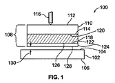
図1は、SAWタッチパネル100を示す。基板102は、表面弾性波またはビームの伝播をサポートする。基板102は、上面104および下面106を有している。SAWを発生しかつ検出するトランスミッタ、アレー、レシーバ等は、基板102の上面104および/または縁部に取付けられまたは形成され、詳しくは以下の通りである。基板102は、ガラス、またはポリスチレンのような音響損失の小さいポリマー、アルミニウムのような金属、またはSAWの伝播可能な他の任意の材料または複合材で形成できる。一般に、SAWは、基板102の上面104へのタッチに感応するレイリー波、準レイリー波、ラム波またはシヤー波または他の種類の弾性波のいずれか1つまたはこれらの組合せを表示するのに使用できる(いくつかの技術文献において「SAW」は「レイリー波」と同義語として使用されているが、本願ではより広義に定義される)。
FIG. 1 shows a SAW
多層カバーシート108は、基板102上に配置される。カバーシート108は3層からなり、かつシングルタッチ並びにマルチタッチ(すなわち、2以上の同時タッチ)、ズーム(拡大)のようなジェスチャ(しぐさ)(但し、ズームに限定されない)の検出をサポートする。タッチ応答は、指先による入力に加え、爪による入力およびクレジットカードおよび他の硬く、しっかりした物体による物体入力によっても行われる。静的なタッチは、保持状態にありかつ接触が維持される限り検出される。外側の荷重分散層110は、上面112および下面114を有している。中間の柔軟層118は、上面120および下面122を有している。柔軟層118の上面120は、荷重分散層110の下面114に結合される。底の抗スティッキング層124は、上面126および下面128を有している。抗スティッキング層124の上面126は、柔軟層118の下面122に結合される。
The
荷重分散層110の上面112は、使用者からのタッチを受ける。前述のように、タッチは、活性を有する指または指先、非活性の爪、クレジットカードまたは他の物体、または図示のようなスタイラス等の物体116を用いて行われるのがよい。一般に、用語「物体116」は、本願では、タッチパネル100に選択を行いまたはデータを入力するのに使用される使用者の手の一部を含むあらゆる物体を意味し、したがって物理的形状および/または図示の形状に限定されるものではない。用語「非活性」は、物体116が、センサ、マグネット、またはタッチを生じさせる必要のない他のデバイスを含まないことを意味するに過ぎない。それどころか、タッチは、最小の接触領域内で行われる荷重分散層I10上への物体116による力に応答する。
The
抗スティッキング層124の下面128と基板102の上面104との間には小さいギャップ130が存在する。物体116のようなタッチが上面112を押したとき、カバーシート108が撓み、抗スティッキング層124の下面128の対応領域は、基板102上を伝達されるSAWを遮断する。下面128が滑らかでない或る実施形態では、タッチが存在しない場合でも、下面128が非常に小さい複数の接触点で基板102の上面104と接触してもよいがタッチ応答は生じない。この場合、設計図面では、下面128と基板の上面104との間のギャップ130のようなギャップは見られないことがある。
There is a
カバーシート108内の層に使用される材料は、耐久性、透明性、加工性または製造容易性、コストおよび圧縮に対する機械的応答性等の特性に基づいて選択されるのがよい。(材料単独のまたは他の材料と対比しての)硬度および剛性についても更に考慮されるのがよい。本願で使用するとき、材料特性を説明するのに、「硬い」、「より硬い」、「柔らかい」および「より柔らかい」が使用される。定められた幾何学的形状をもつ材料の試料の挙動を説明するのに、用語「剛(こわ)い」または「剛性」が使用される。
The material used for the layers in the
基板102上のタッチ接触領域が最小領域を超える場合には、SAW減衰により信頼性ある検出が行われる。この最小領域の量的値は、関連電子部品の作動周波数および感度により定められる。例えば、現在のSAWタッチスクリーン製品の5MHzの作動周波数および電子部品については、最小タッチ接触領域の直径は、一般に2mm〜10mmの範囲内にある。より高い作動周波数では、一般に、最小接触領域はより小さくなる。荷重分散層110は、物体116がどのように尖った形状であっても、加えられた任意のタッチ力すなわちタッチ荷重からの力が少なくとも最小接触領域をカバーするように分散して、SAW減衰の信頼性ある検出が行えるようにする。荷重分散層110は、力を分散させるのに充分な剛性を必要とする(しかしながら、タッチ力が分散し過ぎて正確な座標検出が行えないほど高い剛性ではない)。ここで、「剛性」は、厚さ「t」、ヤング係数「E」およびポアソン比νの均質層について次式で表わされる曲げ剛性すなわち撓み剛性「D」と同義語である。
D=E・t3/{12・(1-ν2)} 式1
荷重分散層110は、ガラスのような大きい値のヤング係数Eをもつ非常に硬い材料、またはポリエチレンテレフタレート(PET)、ポリエチレンナフタレート(PEN)、アクリルまたはマイラー等のポリマーのようなあまり大きくない値のヤング係数Eをもつ材料で形成できる。小さい値のヤング係数Eは、大きい値の層厚tにより補償されるのがよい。例えば、厚さtを2倍にすることで、ヤング係数Eが8分の1に減少する分を補償するのがよい。一実施形態では、荷重分散層110は、50ミクロン〜300ミクロンの範囲の厚さをもつガラスで形成されるのがよい。他の実施形態では、荷重分散層110は、100ミクロン〜600ミクロンの範囲の厚さをもつPETで形成できる。上面112は滑らかで、べとつかないすなわちくっ付き難いものがよい。図1におけるカバーシート108の層厚は、正確な縮尺で示されていないことを理解すべきである。
When the touch contact area on the
D = E · t 3 / {12 · (1−ν 2 )} Equation 1
The
荷重分散層110は、単独では、所望の最小接触領域に亘って密接した音響接触(acoustic contact)を確保できない。しかしながら、柔らかなすなわち柔軟な層を備えた下層を付加することにより、密接した音響接触が保証されるのがよい。柔軟層118は、荷重分散層110と比較して柔らかい(例えば、より小さい値のヤング係数Eを有する)材料で形成するのがよい。柔軟層118が所望の接触領域内の基板102の上面104に適合する能力は、層材料の柔軟性(ヤング係数が小さいこと)並びに柔軟層118の厚さの両方に依存する。一般に、柔軟層118が薄いほど、材料は柔軟にするのがよい。例えば、柔軟層118は、エラストマー材料すなわちエラストマーで形成できかつ感度レベルまたは外側のタッチ表面から基板102への力の伝達に基づいて選択されるのがよく、タッチ応答は、所望の入力物体116並びに所望の透明度レベルを用いて達成される。一実施形態では、柔軟層118はVistalon(商標)EPDMのようなEPDMゴム(エチレンジエンモノマー(Mクラス)ゴム)、プラストマー、Vistamaxx(商標)(プロピレンベースのエラストマー)、Exact(商標)プラストマー(低密度エチレンコポリマー)、ENGAGE 8401のようなENGAGE(商標)ポリオレフィンエラストマー、または所望の特性を有する他の物質で形成するのがよい。柔軟層は、荷重分散層110の下面114上に、コーティングされ、プリンティングされ、ラミネーティングされ、溶融、加熱および/または同時押出しされるのがよい。柔軟層118は、一実施形態では75ミクロン〜500ミクロンの厚さ、他の実施形態では750ミクロンまでの厚さにするのがよい。荷重分散層110および柔軟層118の厚さは、撓みおよび応答のような特性を最大化すべく選択され、かつタッチパネル100の用途、タッチを行うのに使用されると予想される物体の種類等に基づいて定められるのがよい。荷重分散層の下面114は、加熱、積層等により柔軟層118の上面120に結合されるのがよい。選択される材料に基づいて、他の結合方法を使用できることは理解されよう。
The
残念なことに、既知のSAWカバーシートの解決方法は、柔軟層118の材料の選択が制限されるという欠点がある。柔軟性が高い材料は基板の上面104にくっ付き易く、しばしば、物体またはスタイラス116を除去した後でも、いつまでもタッチを検出してしまうという好ましくない問題を引き起こす。このくっ付き易い問題を回避すべく柔軟層118に柔軟性の低い材料を使用すると、しばしば、タッチ感度の損失または好ましくない厚い柔軟層118を使用するという問題を引き起こす。しかしながら、抗スティッキング層124の付加により、柔軟層118が基板102の上面104にくっ付くことが防止される。抗スティッキング層124が充分にフレキシブルであれば、カバーシート108に抗スティッキング層124を設けることにより、スティッキングの問題を解決できると同時に、柔軟層118の柔軟性により基板102との密接な音響接触を妨げない。抗スティッキング層124が非常に薄ければ、比較的硬い材料(例えば、比較的高いヤング係数の値を有する材料)でも充分なフレキシビリティが得られる。抗スティッキング層124は、例えば、抗スティッキングフルオロカーボンソリッドポリマー(またはポリテトラフルオロエチレン)、ポリシロキサンまたはポリマー複合材、インジウム錫酸化物(ITO)、シリカ等の(必要ならば)薄くて透明な金属/無機/セラミック材料等の多くの材料で形成するのがよいが、これらに限定されるものではない。或る実施形態では、抗スティッキング層124は、コーティングまたはフィルムと呼ぶことができるものでもよい。抗スティッキング層124は、抗スティッキング層124は、柔軟層118の下面122に、コーティングされ、蒸着され、スプレーイングされ、プラズマ処理され、プリンティングされ、ラミネーティングされ、加熱、融着および/または同時押出しされることにより形成できる。抗スティッキング層124は、感度を最大化するため、カバーシート108の他の層に比べて比較的薄くするのがよい。或る実施形態では、抗スティッキング層124の厚さは、所望の抗スティッキング性能が得られれば充分であり、例えば10ミクロンまでの厚さにすることができる。この厚さは、少なくとも一部は、材料並びに適用方法により決定されると理解すべきである。或る実施形態では、抗スティッキング層124は、柔軟層118の下面122を完全に覆わなくてもよい。他の実施形態では、抗スティッキング層124は、下面128に或る程度粗面化することができる。
Unfortunately, the known SAW cover sheet solution has the disadvantage that the choice of material for the
図2は、基板102上に配置されたカバーシート108を備えた図1のタッチパネル100を示す。荷重分散層110の上面112には、1つまたは2つ以上の付加層を付加できる。例えば、薄い耐スクラッチポリマー層である硬質コーティング層140を使用するのがよい。硬質コーティング層140は、荷重分散層110の上面112にスクラッチ耐性を付与する。例えば防眩表面処理または反射防止コーティングのような光学層142を使用することもできる。また、撥水性を向上させるため、疎水層144を使用することもできる。一実施形態では、疎水層144は、数分子の厚さにすることができる。これらの層140、142、144の1つ以上を使用できること、および層は図示している順序とは別の順序でも上面112の上に適用できることは理解されよう。図示されてはいないが、スクラッチ耐性および/または保護性を増大させる置換可能な付加「リリースライナ」を、最外層または最外表面に配置することもできる。
FIG. 2 shows the
一実施形態では、基板102の上面104上に、1つまたは2つ以上のスペーサ146を設けるのがよい。スペーサ146は、タッチ表面からタッチが除去された後に、上面104からの抗スティッキング層124の解放を向上させる。
In one embodiment, one or
或る実施形態では、カバーシート108には付加層が設けられるのがよい。図3は、多層カバーシート202を有する別のSAWタッチパネル200を示す。図1に関連して前述した構成要素と同様な構成要素は同じ参照番号で示されている。例えば、カバーシート202は、基板102の上面104上に、ギャップ130の距離を隔てて配置される。
In some embodiments, the
図3に示す実施形態では、カバーシート202は、図1のカバーシート108と比較して2つの付加層を有している。外側の剛い荷重分散層204は上面206および下面208を有している。使用者は、上面206上に物体116を使用して、データを入力しかつタッチパネル200上での選択を行うことができる。第1柔軟層210は、上面212および下面214を有している。第1柔軟層210の上面212は、荷重分散層204の下面208に結合されている。付加荷重分散層216は上面218および下面220を有し、上面218は第1柔軟層210の下面214に結合されている。第2柔軟層222は上面224および下面226を有し、上面224は荷重分散層216の下面220に結合されている。抗スティッキング層228は上面230および下面232を有し、上面230は第2柔軟層222の下面226に結合されている。
In the embodiment shown in FIG. 3, the
荷重分散層204、216は、第1および第2柔軟層210、222と比較して比較的剛くかつ硬い材料で形成されている。荷重分散層204、216は同じ材料または異なる材料で形成でき、第1および第2柔軟層も同じ材料または異なる材料で形成できる。荷重分散層204、216は、図1の荷重分散層110に関して前述したように、ガラス、ガラスマイクロシート、PETまたは他の材料で形成できる。第1および第2柔軟層210、222は、柔軟層118に関して前述した材料で形成できる。抗スティッキング層228は、タッチ(単一回または複数回)により撓んだときに、カバーシート202が基板102の上面104に付着すなわちくっ付くことを防止すべく、抗スティッキング材料で形成される。
The
使用される材料および各層の厚さは、所望の性能、使用が想定される物体116の形式、およびタッチパネル200の機能的使用に基づいて選択されるのがよい。例えば、感度、すなわちカバーシート202を撓ませてタッチ事象を生じさせるのにどれだけの力を必要とするかは、層の厚さ、各層の硬度、カバーシート202の層の数、抗スティッキング層228の特性等に基づいて調節できる。
The materials used and the thickness of each layer may be selected based on the desired performance, the type of
一実施形態では、カバーシート202には付加層(図示せず)、例えば付加柔軟層と対をなすガラスまたはPETで形成された付加荷重分散層を設けることができる。或る実施形態では、より多くの層を用いることにより感度を高めることができる。層が多くなると、基板102の上面104に大きいタッチ領域が生じるからである。また、感度は、物体116のサイズおよび物体の圧力に基づいて変化する。
In one embodiment, the
図1〜図3は、例えば液晶ディスプレイ(LCD)のようなディスプレイの前方に配置されるか、またはディスプレイから分離されたトラックパッドとして機能するように構成されたタッチパネル100、200を示す。これに対し図4は、タッチパネル250のSAWカバーシート270がフレキシブルディスプレイ層252を備えている実施形態を示す。フレキシブルディスプレイの1つのオプションは、有機発光ダイオード(Organic Light Emitting Diode:OLED)ディスプレイである。フレキシブルディスプレイの他の例は、電気泳動ディスプレイ(ElectroPhoretic Display:EPD)である。LCDとは異なり、OLEDおよびEPDは、フレキシブルまたは剛い基板上で組み立てることができ、消費電力が小さく、かつ太陽光のような明るい条件下でより良い性能を有している。
1-3
フレキシブルディスプレイ層252は、上面254および下面256を有している。一実施形態では、フレキシブルディスプレイ層252は100ミクロン厚さのガラス基板のような基板を有し、該基板上に非常に薄いOLEDコンポネンツ(例えばダイオード並びに他のコネクション等)が組付けられるのがよい。OLEDコンポネンツは、例えば50ミクロンのガラス層またはこの均等物のような他の層によりシールされるのがよい。上面254は、物体116からの入力を受けるタッチ感応面である。柔軟層258は上面260および下面262を有し、上面260は、フレキシブルディスプレイ層252の下面256に結合されている。柔軟層258は、前述のようにエラストマー材料で形成するのがよい。抗スティッキング層264は上面266および下面268を有し、上面266は柔軟層258の下面262に結合されている。抗スティッキング層264は抗スティック材料で形成され、前述のように層またはコーティングであるのがよい。基板102の上面104は、抗スティッキング層264の下面268からギャップ130だけ離隔される。
The
フレキシブルディスプレイ層252の基板(図示せず)は、物体116の尖鋭タッチからの力を分散させ、基板102の上面104上に検出可能なタッチ領域を生じさせるのに充分な剛性を有する。図示されてはいないが、フレキシブルディスプレイ層252の上面254を保護するため、付加層および/またはコーティングを使用できる。フレキシブルディスプレイ層252は、荷重分散層として機能するのに充分なフレキシビリティがあればよい。すなわち、不充分なタッチ感度または不充分な座標測定しか得られない程にタッチ力が分散されるような剛性であってはならない。フレキシブルディスプレイ層252は、他の基準、例えばスクロールのように巻き上げられる能力をもつほどフレキシブルである必要はない。
The substrate (not shown) of the
基板102は、以下に述べるように取付けられまたは一体化されたトランスデューサまたは反射アレーを備えたSAW伝播面である。フレキシブルディスプレイ層252は使用者と基板102との間にあるので、基板102は透明でも不透明でもよい。基板102は、ガラスまたは実質的に透明な材料またはアルミニウムのような金属を使用できる。或る実施形態では、金属は、ガラスより良くSAWを伝播しかつガラスより加工が容易である。
The
或る実施形態では、図1〜図4の実施形態には1つ以上の付加介在層を使用できることを理解すべきである。したがって、層は、互いに直接的または間接的に結合するのがよい。 It should be understood that in some embodiments, one or more additional intervening layers can be used in the embodiments of FIGS. Thus, the layers should be bonded directly or indirectly to each other.
図5は、SAWタッチパネルへのSAWカバーシートの取付け構造を示す側断面図である。この例では、図1のカバーシート108と同様の参照番号を用いて説明するが、この取付け方法および構造は他のカバーシートにも使用できる。荷重分散層110、柔軟層118、抗スティッキング層124および基板102が示されている。また、基板102の下面106にはピエゾ280が取付けられ、上面104には回折格子282が取付けられている。他の実施形態では、回折格子282に加えまたは回折格子の代わりに、アレーおよび/またはビームスプリッタが上面104に取付けられる。
FIG. 5 is a side sectional view showing a structure for attaching the SAW cover sheet to the SAW touch panel. In this example, the same reference numerals as those of the
図示の実施形態では、カバーシート108は基板102に接合されている。荷重分散層110および基板102は、両方とも、柔軟層118および抗スティッキング層124の長さを超える長さで延びている。スペーサ284が外縁部286に沿って使用されておりかつ基板102の4辺に沿って全周または部分的に延びている。他の実施形態では、複数の別々のスペーサ284が使用される。スペーサ284は、カバーシート108および基板102を互いに所望の関係に維持すべく、接着剤を用いて荷重分散層110および基板102の両方に接合される。スペーサ284の高さ(例えば、上面104と下面114との間の距離)は、所望のギャップ130を維持するように選択される。一実施形態では、荷重分散層110とスペーサ284との間に黒色または他の色の不透明ペイント288または他の不透明物質が使用され、不透明ペイントは、荷重分散層110と柔軟層118との間に部分的に延びている。これにより、層110、118、124が透明である場合に、ピエゾ280および回折格子282がタッチパネル100の使用者に見えなくすることができる。
In the illustrated embodiment, the
図6は、SAWタッチパネルに対してSAWカバーシートを取付ける構造を示す他の側断面図である。この例では、カバーシート(例えば図1のカバーシート108)は、単一の矩形ブロックとして示されている。抗スティッキング層124の下面128(図1に詳細を示した)のようなカバーシート108は、支持フレーム290に接合される。支持フレーム290は、カバーシート108の全周に亘って延びるように構成されるのがよい。支持フレーム290は、基板102を支持する他の構造体に接合または連結することもできる。例えば、支持フレーム290は、ディスプレイパネルおよびSAWタッチパネルの両方を収容するように設計されたより大きいハウジングの一部として構成するか、該ハウジングと一体に形成することもできる。ピエゾ280は基板102の下面106に結合され、回折格子282は上面104に結合される。
FIG. 6 is another side sectional view showing a structure for attaching the SAW cover sheet to the SAW touch panel. In this example, the cover sheet (eg,
図7は、基板102を包囲する支持フレーム290を明瞭にするための平面図である。この図面にはカバーシート108は示されていない。カバーシート108の外縁部は支持フレーム290に接合または結合され、支持フレーム290に対してカバーシート108を所望の関係に保持する。SAWタッチパネルは、上記特許文献1に開示されたSAWタッチパネルの設計のように、上面104にトランスデューサ構造または反射アレーが存在しない設計にするのが有利である。なお、特許文献1の全体は本願に援用する。
FIG. 7 is a plan view for clarifying the
図8は、コンピュータ354に相互接続されたタッチディスプレイ352を備えたタッチディスプレイシステム350を示すブロック図である。コンピュータ354は、例えばゲームおよび娯楽用ファミリースタイルホームコンピュータシステム、医療画像の視覚化および操作、署名入力または他の手書き入力、コピー機、小売店およびレストランのキャッシュレジスタ等への入力のような1つ以上の用途で作動する。タッチディスプレイ352に加え、コンピュータ354には、キーボードおよび/またはマウス等の他のユーザ入力356を設けることができる。分離して示されているが、タッチディスプレイシステム350のコンポネンツは、例えば携帯情報端末(PDA)、電話機、カメラまたは他のポータブルデバイス等の単一ユニット内に収めることができる。
FIG. 8 is a block diagram illustrating a
タッチディスプレイ352は、ディスプレイスクリーン358上にデータを表示するコンポネンツを含む。ディスプレイスクリーン358は、LCD、陰極線管(CRT)、プラズマディスプレイ、OLED、写真画像等であるのがよい。図1のタッチパネル100または図3のタッチパネル200のようなタッチパネルは、ディスプレイスクリーン358上に取付けられるのがよい。フレキシブルディスプレイ層252(例えば、OLEDディスプレイ層またはEPDディスプレイ層)がタッチパネル250のカバーシート270の一部である図4の実施形態では、ディスプレイスクリーン358は使用されないことは理解されよう。他の実施形態では、タッチパネル100は、トラックパッドとして機能するように、ディスプレイスクリーン358とは物理的に別々に配置される。
ディスプレイケーブル360は、タッチディスプレイ352とディスプレイコントローラ362とを接続している。ディスプレイコントローラ362は、コンピュータ354からビデオケーブル364を介してビデオ情報を受ける。ビデオ情報はディスプレイコントローラ362により受けられかつ処理され、ディスプレイケーブル360を介してタッチディスプレイ352に伝送されてディスプレイスクリーン358上に表示される。タッチディスプレイ352およびディスプレイコントローラ362は、ディスプレイケーブル360が不要になるように配線または相互接続できることは理解されよう。ディスプレイコントローラ362は、中央処理装置(CPU)366およびメモリ368等のコンポネンツを有している。
The
タッチパネルケーブル370は、タッチパネル100とタッチパネルコントローラ372とを相互接続する。タッチパネルコントローラ372は、コンピュータ354から(およびコンピュータ354に)タッチデータケーブル374を介して情報を受け(および送る)。タッチ情報は、タッチパネル100により受けられ、タッチパネルケーブル370を介してタッチパネルコントローラ372に伝送され、次にタッチデータケーブル374を介してコンピュータ354に送られる。タッチパネルコントローラ372は、CPU376およびメモリ378のようなコンポネンツを有している。タッチデータケーブル374およびビデオケーブル364は、無線技術で置換できる。
タッチ検出モジュール380は、タッチパネル100上の1つ以上のタッチを検出する。各タッチは、対応するX座標およびY座標を発生し、或る実施形態ではU座標を発生する。マルチタッチが同時に検出されると、タッチ検出モジュール380はマルチX、Y座標(および任意でU座標)を検出し、これらの座標は、タッチ箇所識別モジュール382により使用されて、適当なXおよびY座標の対を作る。タッチ検出モジュール380およびタッチ箇所識別モジュール382は、コンピュータ354内にあるものとして示されているが、これらのモジュールは、タッチパネルコントローラ372内またはタッチディスプレイシステム350内にも等しく配置することができる。したがって、図8に示す実施形態は例示に過ぎず、これに限定するものではないことを理解すべきである。
The
図9は、ワンタッチまたはマルチ同時タッチを検出すべく上記カバーシートと組み合わせて使用されるSAWタッチパネルの一例を示す平面図である。破線466は基板400の外縁部に沿う境界領域を示し、図5に関連して説明したように、該領域内にカバーシート(図示せず)が基板400に取付けられまたは接合されるのがよい。
FIG. 9 is a plan view showing an example of a SAW touch panel used in combination with the cover sheet to detect one touch or multiple simultaneous touches. Dashed
タッチパネルの基板400は表面弾性波またはビームの伝播をサポートしかつガラス、金属、音響損失の小さいポリマーまたは前述のような他の材料で作られるのがよい。基板400は、この中央部に位置するタッチ領域402を有している。基板400には、X送信トランスデューサ404およびY送信トランスデューサ406およびY受信トランスデューサ408およびX受信トランスデューサ410が取付けられている。送信トランスデューサ404、406および受信トランスデューサ408、410は、ウェッジトランスデューサ、回折格子トランスデューサ、インターデジタルトランスデューサまたは他の任意の形式のトランスデューサで構成できる。送信トランスデューサ404、406は、基板400内で表面弾性波を励振させる。励振された表面弾性波は、送信ビームまたは送信SAWビームとも呼ばれる。第1Xアレー412および第2Xアレー414および第1Yアレー416、第2Yアレー418は、タッチ領域402の外縁部420に近接して基板400に取付けられおよび/または組み立てられている。Xアレー412およびYアレー416は、送信ビームまたは弾性波を、タッチ領域402に向けて例えば90°の角度で偏向させる。Xアレー414およびYアレー418は、タッチ領域402からのビームを例えば90°の角度で偏向させる。X送信トランスデューサ404および第1Xアレー412はともに第1トランスミッタ422であると考えられ、Y送信トランスデューサ406および第1Yアレー412はともに第2トランスミッタ424であると考えられる。また、X受信トランスデューサ410および第2Xアレー414はともに第1レシーバ426であると考えられ、Y受信トランスデューサ408および第2Yアレー418はともに第2レシーバ428であると考えられる。
The
一実施形態では、任意であるが、第1、第2、第3および第4ビームスプリッタ430、432、434および436を、第1および第2Xアレー412、414および第1および第2Yアレー416、418と、タッチ領域402との間で、それぞれ基板400に組付けることができる(例えばエッチングまたは蒸着による。但しこれらに限定されない)。第1、第2、第3および第4ビームスプリッタ430〜436は、各々複数の偏向要素438を有している。ビームスプリッタ430〜436は信号のU成分を発生させるのに使用され、したがってXおよびYのみが検出される実施形態では不要である。例えば、ビームスプリッタ430〜436は、多数の同時タッチをサポートする実施形態で使用される。
In one embodiment, optionally, the first, second, third, and
例えば、送信トランスデューサ404は、第1Xアレー412に沿ってSAWビーム440を送信する。第1Xアレー412は、偏向ビーム442で示すように、SAWビーム440の一部を90°の角度で偏向させる。偏向されたビーム442は第1ビームスプリッタ430に入りかつ偏向要素438により少なくとも2つの異なるビーム(例えば偏向されないビーム444および偏向されたUビーム446)に分割される(或いは、第1Xアレー412は、SAWビーム440を143°だけ偏向させ、これにより偏向されたビーム442は図示した偏向されたUビーム446に平行な第1ビームスプリッタ430に入るようにしてもよい。この例では、第1ビームスプリッタ430は、偏向されたUビーム446として偏向されたビーム442の変更されない一部を通すと同時に、偏向されないビーム444を偏向させる)。第1Xアレー412の長さに沿って形成された多数の偏向されたビーム442があり、これにより、多数の変更されないビーム444および偏向されたUビーム446が基板400のタッチ領域402内のタッチ事象を検出することを理解すべきである。偏向されないビーム444は偏向されたビーム442と同じ経路および方向に沿って進行を続け偏向されたUビーム446はU方向または斜め方向に沿って送られる。
For example, the transmit
同様に、Y送信トランスデューサ406は、SAWビーム450(その一部は、偏向されたビーム452として第1Yアレー416により90°の角度で偏向されている)を送信する。偏向されたビーム452は第2ビームスプリッタ432に入りかつ偏向されないビーム454および偏向されたUビーム456に分割される。偏向されないビーム454は偏向されたビーム452の元の経路上を進行し続け、一方、偏向されたUビーム456は偏向されないビーム454または弾性波に対して一定角度(例えば約37°)で偏向される。
Similarly, Y transmit
偏向されないビーム444はタッチ領域402を横切って進みかつ第3ビームスプリッタを通る。第2Xアレー414は、偏向されないビーム444を90°の角度で偏向させて、戻りビーム460を形成し、該戻りビーム460はX受信トランスデューサ410により受けられる。偏向されたUビーム446はタッチ領域402を通って斜め方向に送られ、第4ビームスプリッタ436に出合う。この場合、第4ビームスプリッタ436は入射するビームを分割するが、偏向された部分のみが使用される。第4ビームスプリッタ436は、分割され、したがって互いに異なる角度で第4ビームスプリッタ436に入るマルチビームを受ける。第4ビームスプリッタ436は、偏向されたUビーム446を約37°の角度で偏向させる。偏向されたUビームは第2Yアレー418に入りかつ戻りビーム462としてY受信トランスデューサ408に向かって90°だけ偏向される。
The
第1〜第4ビームスプリッタ430〜436は、所望のビームスプリット機能が得られる任意の構造にすることができる。一実施形態では、ビームスプリッタ430〜436は、同じ材料および方法を用いて、反射アレー412〜418と同時にまたは別々に作られる。ビームスプリッタ430〜436は、反射アレー412〜418と同じまたは異なる高さにすることができる。或いは、ビームスプリッタ430〜436の偏向要素438は、めっき材料またはエッチングガラスの反射ラインセグメント464を有するのがよい。
The first to
他の実施形態では、XYUアレー設計は、別々の送信トランスデューサにより直接照射される基板400の各送信側に沿う別々の送信Uアレーと、別々の受信トランスデューサを直接照射する受信Uアレーとを有する。
In other embodiments, the XYU array design has a separate transmit U array along each transmit side of the
上記カバーシートの実施形態は、異なる作動周波数で使用できる。例えば、マルチタッチ用途をサポートするには、より高い作動周波数を選択できる。より高い周波数では、より薄いSAWサポート基板を使用でき、或る実施形態では感度が高められる。より低い作動周波数では、より大きい全体的センササイズを達成でき、これにより、トランスデューサおよびアレーの構造をより容易に製造できる。 The cover sheet embodiments can be used at different operating frequencies. For example, a higher operating frequency can be selected to support multi-touch applications. At higher frequencies, thinner SAW support substrates can be used, and in some embodiments the sensitivity is increased. At lower operating frequencies, a larger overall sensor size can be achieved, which makes it easier to manufacture transducer and array structures.
上記説明は例示であり、限定するものではないことを理解すべきである。例えば、上記実施形態(および/またはその特徴)は互いに組合せて使用される。また、本発明の範囲から逸脱することなく特定の状況または材料を本発明の教示に適合させるため、多くの変更を行うことができる。本願で説明する寸法および材料の種類は、本発明のパラメータを定めるものであることを意図するが、これらはいかなる意味においても限定的なものではなく、例示実施形態である。上記説明を読むことにより、当業者には他の多くの実施形態が明らかになるであろう。本発明の範囲は、特許請求の範囲の記載およびその均等物を参照して決定すべきである。特許請求の範囲の記載において、用語「含む」および「ここで」は、それぞれ「備える」および「おける」の平易な英語の同義語として使用される。また、用語「第1」、「第2」および「第3」等は、単なるラベルとして使用されており、これらの対象物に番号の条件を賦課するものではない。 It should be understood that the above description is illustrative and not restrictive. For example, the above-described embodiments (and / or features thereof) are used in combination with each other. In addition, many modifications may be made to adapt a particular situation or material to the teachings of the invention without departing from the scope of the invention. While the dimensions and material types described herein are intended to define the parameters of the present invention, they are not limiting in any way and are exemplary embodiments. Many other embodiments will be apparent to those of skill in the art upon reading the above description. The scope of the present invention should be determined with reference to the appended claims and their equivalents. In the claims, the terms “comprising” and “here” are used as plain English synonyms for “comprising” and “in” respectively. Further, the terms “first”, “second”, “third”, and the like are used merely as labels, and do not impose any numbering conditions on these objects.
100 SAWタッチパネル
102 基板
108 多層カバーシート
110 荷重分散層
116 物体
118 柔軟層
124 抗スティッキング層
130 ギャップ
140 硬質コーティング層
142 光学層
144 疎水層
146 スペーサ
DESCRIPTION OF
Claims (16)
前記基板上に配置されるように構成された多層カバーシートとを有し、前記カバーシートは、
上面および下面を備えた荷重分散層を有し、前記荷重分散層の上面は、物体からのタッチ入力を受けるように構成され、
上面および下面を備えた柔軟層を有し、前記柔軟層の上面は前記荷重分散層の下面に結合されるように構成され、
上面および下面を備えた抗スティッキング層を有し、前記抗スティッキング層の上面は前記柔軟層の下面に結合されるように構成され、前記抗スティッキング層の下面は前記基板の上面に近接して配置されるように構成されていることを特徴とするタッチパネル。 A surface acoustic wave propagation substrate having an upper surface and a lower surface;
A multilayer cover sheet configured to be disposed on the substrate, the cover sheet comprising:
A load distribution layer having an upper surface and a lower surface, wherein the upper surface of the load distribution layer is configured to receive touch input from an object;
A flexible layer having an upper surface and a lower surface, wherein the upper surface of the flexible layer is configured to be coupled to the lower surface of the load distribution layer;
An anti-sticking layer having an upper surface and a lower surface, wherein the upper surface of the anti-sticking layer is configured to be bonded to the lower surface of the flexible layer, and the lower surface of the anti-sticking layer is disposed adjacent to the upper surface of the substrate A touch panel that is configured to be configured.
前記基板上に配置されるように構成された多層カバーシートとを有し、前記カバーシートが、
上面および下面を備えかつ画像を表示するように構成されたフレキシブルディスプレイ層を有し、前記フレキシブルディスプレイ層の上面は物体からのタッチ入力を受けるように構成され、
上面および下面を備えた柔軟層を有し、前記柔軟層の上面は前記フレキシブルディスプレイ層の下面に結合されるように構成され、
上面および下面を備えた抗スティッキング層を更に有し、前記抗スティッキング層の上面は前記柔軟層の下面に結合されるように構成され、前記抗スティッキング層の下面は前記基板の上面に近接して配置されるように構成されていることを特徴とするタッチパネル。 A surface acoustic wave propagation substrate having an upper surface and a lower surface;
A multilayer cover sheet configured to be disposed on the substrate, the cover sheet comprising:
A flexible display layer having an upper surface and a lower surface and configured to display an image, wherein the upper surface of the flexible display layer is configured to receive touch input from an object;
A flexible layer having an upper surface and a lower surface, wherein the upper surface of the flexible layer is configured to be coupled to the lower surface of the flexible display layer;
An anti-sticking layer having an upper surface and a lower surface, wherein the upper surface of the anti-sticking layer is configured to be bonded to the lower surface of the flexible layer, and the lower surface of the anti-sticking layer is adjacent to the upper surface of the substrate. A touch panel configured to be arranged.
Applications Claiming Priority (3)
| Application Number | Priority Date | Filing Date | Title |
|---|---|---|---|
| US12/789,733 | 2010-05-28 | ||
| US12/789,733 US8638318B2 (en) | 2010-05-28 | 2010-05-28 | Multi-layer coversheet for saw touch panel |
| PCT/US2011/037446 WO2011149793A1 (en) | 2010-05-28 | 2011-05-20 | Multi-layer coversheet for saw touch panel |
Publications (2)
| Publication Number | Publication Date |
|---|---|
| JP2013528874A true JP2013528874A (en) | 2013-07-11 |
| JP2013528874A5 JP2013528874A5 (en) | 2014-01-09 |
Family
ID=44504443
Family Applications (1)
| Application Number | Title | Priority Date | Filing Date |
|---|---|---|---|
| JP2013513206A Pending JP2013528874A (en) | 2010-05-28 | 2011-05-20 | Multilayer cover sheet for surface acoustic wave (SAW) touch panel |
Country Status (6)
| Country | Link |
|---|---|
| US (1) | US8638318B2 (en) |
| EP (1) | EP2577433B1 (en) |
| JP (1) | JP2013528874A (en) |
| CN (1) | CN103097999B (en) |
| TW (1) | TWI472990B (en) |
| WO (1) | WO2011149793A1 (en) |
Cited By (1)
| Publication number | Priority date | Publication date | Assignee | Title |
|---|---|---|---|---|
| TWI775250B (en) * | 2020-12-21 | 2022-08-21 | 達方電子股份有限公司 | Backlight module |
Families Citing this family (38)
| Publication number | Priority date | Publication date | Assignee | Title |
|---|---|---|---|---|
| US10198097B2 (en) | 2011-04-26 | 2019-02-05 | Sentons Inc. | Detecting touch input force |
| US9477350B2 (en) | 2011-04-26 | 2016-10-25 | Sentons Inc. | Method and apparatus for active ultrasonic touch devices |
| US9639213B2 (en) | 2011-04-26 | 2017-05-02 | Sentons Inc. | Using multiple signals to detect touch input |
| US9189109B2 (en) | 2012-07-18 | 2015-11-17 | Sentons Inc. | Detection of type of object used to provide a touch contact input |
| US11327599B2 (en) | 2011-04-26 | 2022-05-10 | Sentons Inc. | Identifying a contact type |
| US8736574B2 (en) * | 2011-05-19 | 2014-05-27 | Microsoft Corporation | Pressure-sensitive multi-touch device |
| US9372588B2 (en) * | 2011-05-19 | 2016-06-21 | Microsoft Technology Licensing, Llc | Pressure-sensitive multi-touch device |
| FR2978570B1 (en) * | 2011-07-28 | 2013-08-16 | Commissariat Energie Atomique | SYSTEM AND METHOD FOR DETECTING AND LOCATING A DISTURBANCE OF A MEDIUM |
| CN104169848B (en) | 2011-11-18 | 2017-10-20 | 森顿斯公司 | Detect touch input force |
| US9449476B2 (en) | 2011-11-18 | 2016-09-20 | Sentons Inc. | Localized haptic feedback |
| US10235004B1 (en) | 2011-11-18 | 2019-03-19 | Sentons Inc. | Touch input detector with an integrated antenna |
| US9348468B2 (en) | 2013-06-07 | 2016-05-24 | Sentons Inc. | Detecting multi-touch inputs |
| US9524063B2 (en) | 2012-07-18 | 2016-12-20 | Sentons Inc. | Detection of a number of touch contacts of a multi-touch input |
| US9078066B2 (en) | 2012-07-18 | 2015-07-07 | Sentons Inc. | Touch input surface speaker |
| US9466783B2 (en) | 2012-07-26 | 2016-10-11 | Immersion Corporation | Suspension element having integrated piezo material for providing haptic effects to a touch screen |
| CN103576995A (en) * | 2012-07-31 | 2014-02-12 | 电子触控产品解决方案公司 | Touch sensitive display with acoustic isolation |
| US9551783B2 (en) * | 2013-06-03 | 2017-01-24 | Qualcomm Incorporated | Display with backside ultrasonic sensor array |
| CN103442104B (en) * | 2013-08-21 | 2016-07-06 | 上海鼎为通讯电子有限公司 | Mobile terminal and display control method thereof |
| US9588552B2 (en) | 2013-09-11 | 2017-03-07 | Sentons Inc. | Attaching electrical components using non-conductive adhesive |
| US9459715B1 (en) | 2013-09-20 | 2016-10-04 | Sentons Inc. | Using spectral control in detecting touch input |
| US9880671B2 (en) | 2013-10-08 | 2018-01-30 | Sentons Inc. | Damping vibrational wave reflections |
| US9213409B2 (en) | 2013-11-25 | 2015-12-15 | Immersion Corporation | Dual stiffness suspension system |
| CN104866016A (en) * | 2014-02-25 | 2015-08-26 | 曾林 | Separating type mobile equipment |
| CN104850180A (en) * | 2014-02-25 | 2015-08-19 | 曾林 | Separate mobile equipment |
| WO2016044078A1 (en) * | 2014-09-15 | 2016-03-24 | 3M Innovative Properties Company | Multilayer oled cover sheet |
| KR102088674B1 (en) * | 2014-11-27 | 2020-03-13 | 삼성전자주식회사 | flexible display device |
| US9632582B2 (en) | 2014-12-22 | 2017-04-25 | Immersion Corporation | Magnetic suspension system for touch screens and touch surfaces |
| US9589432B2 (en) | 2014-12-22 | 2017-03-07 | Immersion Corporation | Haptic actuators having programmable magnets with pre-programmed magnetic surfaces and patterns for producing varying haptic effects |
| US10048811B2 (en) | 2015-09-18 | 2018-08-14 | Sentons Inc. | Detecting touch input provided by signal transmitting stylus |
| US10908741B2 (en) | 2016-11-10 | 2021-02-02 | Sentons Inc. | Touch input detection along device sidewall |
| US10296144B2 (en) | 2016-12-12 | 2019-05-21 | Sentons Inc. | Touch input detection with shared receivers |
| US10275032B2 (en) | 2016-12-22 | 2019-04-30 | Immersion Corporation | Pressure-sensitive suspension system for a haptic device |
| US10126877B1 (en) | 2017-02-01 | 2018-11-13 | Sentons Inc. | Update of reference data for touch input detection |
| US10585522B2 (en) | 2017-02-27 | 2020-03-10 | Sentons Inc. | Detection of non-touch inputs using a signature |
| US11157115B2 (en) * | 2017-03-31 | 2021-10-26 | Apple Inc. | Composite cover material for sensitivity improvement of ultrasonic touch screens |
| US11580829B2 (en) | 2017-08-14 | 2023-02-14 | Sentons Inc. | Dynamic feedback for haptics |
| US11009411B2 (en) | 2017-08-14 | 2021-05-18 | Sentons Inc. | Increasing sensitivity of a sensor using an encoded signal |
| US11960693B1 (en) | 2023-05-23 | 2024-04-16 | Rockwell Collins, Inc. | Resistive touch sensor with improved force uniformity |
Citations (4)
| Publication number | Priority date | Publication date | Assignee | Title |
|---|---|---|---|---|
| US5451723A (en) * | 1993-10-18 | 1995-09-19 | Carroll Touch, Inc. | Acoustic wave touch panel for use with a non-active stylus |
| JP2007079737A (en) * | 2005-09-12 | 2007-03-29 | Fujitsu Ltd | Touch panel device |
| JP2007199988A (en) * | 2006-01-26 | 2007-08-09 | Seiko Epson Corp | Electro-optical device and electronic device |
| JP2009003672A (en) * | 2007-06-21 | 2009-01-08 | Seiko Epson Corp | Touch panel device, electro-optical apparatus and electronic apparatus |
Family Cites Families (28)
| Publication number | Priority date | Publication date | Assignee | Title |
|---|---|---|---|---|
| US4746914A (en) | 1985-02-05 | 1988-05-24 | Zenith Electronics Corporation | Cathode ray tube for use in a touch panel display system |
| US5109177A (en) * | 1989-11-28 | 1992-04-28 | Tektronix, Inc. | Damped cradle for saw device |
| US5243148A (en) * | 1990-11-16 | 1993-09-07 | Exzec, Inc. | Touch panel for an acoustic touch position sensor using shear wave propagation |
| US7663607B2 (en) * | 2004-05-06 | 2010-02-16 | Apple Inc. | Multipoint touchscreen |
| US7006081B2 (en) * | 2000-10-20 | 2006-02-28 | Elo Touchsystems, Inc. | Acoustic touch sensor with laminated substrate |
| US20020149571A1 (en) * | 2001-04-13 | 2002-10-17 | Roberts Jerry B. | Method and apparatus for force-based touch input |
| US6741237B1 (en) * | 2001-08-23 | 2004-05-25 | Rockwell Automation Technologies, Inc. | Touch screen |
| US6793093B2 (en) * | 2001-11-30 | 2004-09-21 | Tung-Hung Tsai | Anti-stick cookware with cookware body formed by spinning |
| JP4198527B2 (en) * | 2003-05-26 | 2008-12-17 | 富士通コンポーネント株式会社 | Touch panel and display device |
| JP2005117313A (en) * | 2003-10-07 | 2005-04-28 | Fujitsu Ltd | Piezo-electric element and touch panel device |
| KR101132103B1 (en) * | 2005-11-30 | 2012-04-05 | 세이코 인스트루 가부시키가이샤 | Bonding method and method for manufacturing display device |
| US20090162645A1 (en) * | 2005-12-05 | 2009-06-25 | Seiko Instruments Inc. | Display Apparatus and Method of Manufacturing a Display Apparatus |
| JP4506742B2 (en) * | 2006-01-27 | 2010-07-21 | エプソンイメージングデバイス株式会社 | Touch panel, electro-optical device and electronic apparatus |
| US8780053B2 (en) * | 2007-03-21 | 2014-07-15 | Northwestern University | Vibrating substrate for haptic interface |
| US7764276B2 (en) * | 2006-04-18 | 2010-07-27 | Schermerhorn Jerry D | Touch control system and apparatus with multiple acoustic coupled substrates |
| JP4809130B2 (en) * | 2006-05-31 | 2011-11-09 | タッチパネル・システムズ株式会社 | Acoustic wave type touch panel |
| TWI315842B (en) * | 2006-07-10 | 2009-10-11 | Egalax Empia Technology Inc | Surface acoustic wave touch panel with interdigital transducers |
| JP2008040608A (en) * | 2006-08-02 | 2008-02-21 | Fujitsu Component Ltd | Surface acoustic wave system touch panel |
| KR100803400B1 (en) | 2006-08-17 | 2008-02-14 | 김찬회 | Protection panel for ultrasonic touch screen and the method |
| US20080180399A1 (en) * | 2007-01-31 | 2008-07-31 | Tung Wan Cheng | Flexible Multi-touch Screen |
| US8144453B2 (en) * | 2007-03-15 | 2012-03-27 | F-Origin, Inc. | Integrated feature for friction less movement of force sensitive touch screen |
| CN101373415B (en) * | 2007-08-21 | 2010-06-02 | 禾瑞亚科技股份有限公司 | Surface acoustic wave type sensing apparatus of touching control panel |
| US20110084941A1 (en) * | 2007-09-20 | 2011-04-14 | Egalax_Empia Technology Inc. | Sensing device of surface acoustic wave touch panel |
| JP5158092B2 (en) * | 2007-11-28 | 2013-03-06 | 株式会社村田製作所 | Elastic wave device |
| EP2078604A1 (en) | 2008-01-10 | 2009-07-15 | Siemens Aktiengesellschaft | Operating device for a compactor and compactor with an operating device |
| US8842076B2 (en) * | 2008-07-07 | 2014-09-23 | Rockstar Consortium Us Lp | Multi-touch touchscreen incorporating pen tracking |
| KR101030497B1 (en) * | 2008-12-26 | 2011-04-21 | 전자부품연구원 | Input device for flexible display device, manufacturing method thereof and flexible display device using the same |
| US8576202B2 (en) | 2010-03-25 | 2013-11-05 | Elo Touch Solutions, Inc. | Bezel-less acoustic touch apparatus |
-
2010
- 2010-05-28 US US12/789,733 patent/US8638318B2/en active Active
-
2011
- 2011-05-20 WO PCT/US2011/037446 patent/WO2011149793A1/en active Application Filing
- 2011-05-20 EP EP11735710.3A patent/EP2577433B1/en active Active
- 2011-05-20 JP JP2013513206A patent/JP2013528874A/en active Pending
- 2011-05-20 CN CN201180037053.5A patent/CN103097999B/en active Active
- 2011-05-27 TW TW100118596A patent/TWI472990B/en not_active IP Right Cessation
Patent Citations (4)
| Publication number | Priority date | Publication date | Assignee | Title |
|---|---|---|---|---|
| US5451723A (en) * | 1993-10-18 | 1995-09-19 | Carroll Touch, Inc. | Acoustic wave touch panel for use with a non-active stylus |
| JP2007079737A (en) * | 2005-09-12 | 2007-03-29 | Fujitsu Ltd | Touch panel device |
| JP2007199988A (en) * | 2006-01-26 | 2007-08-09 | Seiko Epson Corp | Electro-optical device and electronic device |
| JP2009003672A (en) * | 2007-06-21 | 2009-01-08 | Seiko Epson Corp | Touch panel device, electro-optical apparatus and electronic apparatus |
Cited By (1)
| Publication number | Priority date | Publication date | Assignee | Title |
|---|---|---|---|---|
| TWI775250B (en) * | 2020-12-21 | 2022-08-21 | 達方電子股份有限公司 | Backlight module |
Also Published As
| Publication number | Publication date |
|---|---|
| WO2011149793A1 (en) | 2011-12-01 |
| CN103097999A (en) | 2013-05-08 |
| TWI472990B (en) | 2015-02-11 |
| EP2577433A1 (en) | 2013-04-10 |
| US20110291996A1 (en) | 2011-12-01 |
| US8638318B2 (en) | 2014-01-28 |
| EP2577433B1 (en) | 2018-10-17 |
| CN103097999B (en) | 2016-05-04 |
| TW201209683A (en) | 2012-03-01 |
Similar Documents
| Publication | Publication Date | Title |
|---|---|---|
| EP2577433B1 (en) | Multi-layer coversheet for saw touch panel | |
| US8648815B2 (en) | Touch panel that has an image layer and detects bending waves | |
| KR100870793B1 (en) | Touch panel, electro-optic device, and manufacturing method for electro-optic device | |
| US7593067B2 (en) | Electro-optical device and electronic equipment having touch panel with resin having particular elastic modulus | |
| JP6833795B2 (en) | Touch display module and electronic devices that apply this touch display module | |
| US20150286332A1 (en) | Force imaging input device and system | |
| US9069384B2 (en) | Electronic device | |
| US20150331517A1 (en) | Force Detection in Touch Devices Using Piezoelectric Sensors | |
| EP1818790A2 (en) | Touch panel, method for detecting touch input position, electro-optic device, and electronic device | |
| JP2010231783A (en) | Touch screen module with protector window | |
| US20140009429A1 (en) | Method of producing capacitive coplanar touch panel devices with laser ablation | |
| TW200825877A (en) | Touch panel input device | |
| CN106020540A (en) | Touch module, a touch pressure sensing method and electronic device | |
| KR20150144913A (en) | Flexible display device | |
| JP2017223834A (en) | Backlight device and display device including the same | |
| JP2011175528A (en) | Display device having touch panel | |
| KR20100019810A (en) | Touch screen system | |
| KR20160061170A (en) | Flexible Display Appartus | |
| KR20160124541A (en) | Flexible Display Appartus | |
| JP4562578B2 (en) | Touch panel and touch panel type coordinate input method | |
| US9483130B2 (en) | Touch device | |
| CN109598233B (en) | Display device with fingerprint identification function | |
| JP2009003672A (en) | Touch panel device, electro-optical apparatus and electronic apparatus | |
| KR20160032984A (en) | Touch Sensor |
Legal Events
| Date | Code | Title | Description |
|---|---|---|---|
| A521 | Request for written amendment filed |
Free format text: JAPANESE INTERMEDIATE CODE: A523 Effective date: 20131114 |
|
| A871 | Explanation of circumstances concerning accelerated examination |
Free format text: JAPANESE INTERMEDIATE CODE: A871 Effective date: 20131114 |
|
| A975 | Report on accelerated examination |
Free format text: JAPANESE INTERMEDIATE CODE: A971005 Effective date: 20131209 |
|
| A131 | Notification of reasons for refusal |
Free format text: JAPANESE INTERMEDIATE CODE: A131 Effective date: 20131216 |
|
| A601 | Written request for extension of time |
Free format text: JAPANESE INTERMEDIATE CODE: A601 Effective date: 20140317 |
|
| A602 | Written permission of extension of time |
Free format text: JAPANESE INTERMEDIATE CODE: A602 Effective date: 20140325 |
|
| A521 | Request for written amendment filed |
Free format text: JAPANESE INTERMEDIATE CODE: A523 Effective date: 20140616 |
|
| A02 | Decision of refusal |
Free format text: JAPANESE INTERMEDIATE CODE: A02 Effective date: 20140922 |