JP2013509619A - Optical device with antistatic properties - Google Patents
Optical device with antistatic properties Download PDFInfo
- Publication number
- JP2013509619A JP2013509619A JP2012537067A JP2012537067A JP2013509619A JP 2013509619 A JP2013509619 A JP 2013509619A JP 2012537067 A JP2012537067 A JP 2012537067A JP 2012537067 A JP2012537067 A JP 2012537067A JP 2013509619 A JP2013509619 A JP 2013509619A
- Authority
- JP
- Japan
- Prior art keywords
- optical
- optical device
- optical member
- film
- antistatic layer
- Prior art date
- Legal status (The legal status is an assumption and is not a legal conclusion. Google has not performed a legal analysis and makes no representation as to the accuracy of the status listed.)
- Withdrawn
Links
- 230000003287 optical effect Effects 0.000 title claims abstract description 205
- 239000000203 mixture Substances 0.000 claims abstract description 61
- 150000003839 salts Chemical class 0.000 claims abstract description 36
- 239000000178 monomer Substances 0.000 claims abstract description 25
- 229920000642 polymer Polymers 0.000 claims abstract description 19
- 150000001450 anions Chemical class 0.000 claims abstract description 9
- 239000007795 chemical reaction product Substances 0.000 claims abstract description 4
- 239000010408 film Substances 0.000 claims description 101
- NIXOWILDQLNWCW-UHFFFAOYSA-M Acrylate Chemical compound [O-]C(=O)C=C NIXOWILDQLNWCW-UHFFFAOYSA-M 0.000 claims description 33
- 229910052757 nitrogen Inorganic materials 0.000 claims description 30
- -1 cycloaliphatic Chemical group 0.000 claims description 27
- 239000012788 optical film Substances 0.000 claims description 22
- IJGRMHOSHXDMSA-UHFFFAOYSA-N nitrogen Substances N#N IJGRMHOSHXDMSA-UHFFFAOYSA-N 0.000 claims description 19
- 230000009477 glass transition Effects 0.000 claims description 16
- RZVINYQDSSQUKO-UHFFFAOYSA-N 2-phenoxyethyl prop-2-enoate Chemical class C=CC(=O)OCCOC1=CC=CC=C1 RZVINYQDSSQUKO-UHFFFAOYSA-N 0.000 claims description 12
- NINIDFKCEFEMDL-UHFFFAOYSA-N Sulfur Chemical group [S] NINIDFKCEFEMDL-UHFFFAOYSA-N 0.000 claims description 10
- 239000011324 bead Substances 0.000 claims description 10
- 229910052717 sulfur Chemical group 0.000 claims description 10
- 239000011593 sulfur Chemical group 0.000 claims description 10
- OAICVXFJPJFONN-UHFFFAOYSA-N Phosphorus Chemical compound [P] OAICVXFJPJFONN-UHFFFAOYSA-N 0.000 claims description 8
- 229910052698 phosphorus Inorganic materials 0.000 claims description 8
- 239000011574 phosphorus Substances 0.000 claims description 8
- 150000001875 compounds Chemical class 0.000 claims description 7
- 238000009792 diffusion process Methods 0.000 claims description 7
- KRHYYFGTRYWZRS-UHFFFAOYSA-M Fluoride anion Chemical compound [F-] KRHYYFGTRYWZRS-UHFFFAOYSA-M 0.000 claims description 5
- 125000000217 alkyl group Chemical group 0.000 claims description 5
- 125000003118 aryl group Chemical group 0.000 claims description 5
- QVGXLLKOCUKJST-UHFFFAOYSA-N atomic oxygen Chemical group [O] QVGXLLKOCUKJST-UHFFFAOYSA-N 0.000 claims description 5
- 229910052760 oxygen Inorganic materials 0.000 claims description 5
- 239000001301 oxygen Chemical group 0.000 claims description 5
- 125000001931 aliphatic group Chemical group 0.000 claims description 4
- 125000004122 cyclic group Chemical group 0.000 claims description 3
- JZMPIUODFXBXSC-UHFFFAOYSA-N ethyl carbamate;prop-2-enoic acid Chemical compound OC(=O)C=C.OC(=O)C=C.CCOC(N)=O JZMPIUODFXBXSC-UHFFFAOYSA-N 0.000 claims description 3
- 229920002635 polyurethane Polymers 0.000 claims description 3
- 239000004814 polyurethane Substances 0.000 claims description 3
- RWSOTUBLDIXVET-UHFFFAOYSA-N Dihydrogen sulfide Chemical class S RWSOTUBLDIXVET-UHFFFAOYSA-N 0.000 claims description 2
- JUJWROOIHBZHMG-UHFFFAOYSA-N Pyridine Chemical class C1=CC=NC=C1 JUJWROOIHBZHMG-UHFFFAOYSA-N 0.000 claims description 2
- 125000002877 alkyl aryl group Chemical group 0.000 claims description 2
- 150000003863 ammonium salts Chemical class 0.000 claims description 2
- 125000004432 carbon atom Chemical group C* 0.000 claims description 2
- 229910052736 halogen Inorganic materials 0.000 claims description 2
- 150000002367 halogens Chemical class 0.000 claims description 2
- 125000005842 heteroatom Chemical group 0.000 claims description 2
- 150000004693 imidazolium salts Chemical class 0.000 claims description 2
- 150000003949 imides Chemical class 0.000 claims description 2
- 150000004714 phosphonium salts Chemical class 0.000 claims description 2
- CERQOIWHTDAKMF-UHFFFAOYSA-M Methacrylate Chemical compound CC(=C)C([O-])=O CERQOIWHTDAKMF-UHFFFAOYSA-M 0.000 claims 3
- 230000001588 bifunctional effect Effects 0.000 claims 2
- QJGQUHMNIGDVPM-UHFFFAOYSA-N nitrogen group Chemical group [N] QJGQUHMNIGDVPM-UHFFFAOYSA-N 0.000 claims 1
- 150000003242 quaternary ammonium salts Chemical group 0.000 claims 1
- 238000000576 coating method Methods 0.000 description 90
- 239000011248 coating agent Substances 0.000 description 82
- 239000010410 layer Substances 0.000 description 79
- XLYOFNOQVPJJNP-UHFFFAOYSA-N water Substances O XLYOFNOQVPJJNP-UHFFFAOYSA-N 0.000 description 43
- 239000000463 material Substances 0.000 description 41
- 239000000523 sample Substances 0.000 description 36
- 238000009472 formulation Methods 0.000 description 34
- 239000007787 solid Substances 0.000 description 34
- 238000000034 method Methods 0.000 description 32
- YMWUJEATGCHHMB-UHFFFAOYSA-N Dichloromethane Chemical compound ClCCl YMWUJEATGCHHMB-UHFFFAOYSA-N 0.000 description 24
- 239000008367 deionised water Substances 0.000 description 23
- 229910021641 deionized water Inorganic materials 0.000 description 23
- 239000008199 coating composition Substances 0.000 description 22
- LAQYHRQFABOIFD-UHFFFAOYSA-N 2-methoxyhydroquinone Chemical compound COC1=CC(O)=CC=C1O LAQYHRQFABOIFD-UHFFFAOYSA-N 0.000 description 18
- CSCPPACGZOOCGX-UHFFFAOYSA-N Acetone Chemical compound CC(C)=O CSCPPACGZOOCGX-UHFFFAOYSA-N 0.000 description 18
- 239000000243 solution Substances 0.000 description 18
- 238000012360 testing method Methods 0.000 description 17
- CSNNHWWHGAXBCP-UHFFFAOYSA-L Magnesium sulfate Chemical compound [Mg+2].[O-][S+2]([O-])([O-])[O-] CSNNHWWHGAXBCP-UHFFFAOYSA-L 0.000 description 16
- 238000006243 chemical reaction Methods 0.000 description 15
- 238000002360 preparation method Methods 0.000 description 15
- KFZMGEQAYNKOFK-UHFFFAOYSA-N Isopropanol Chemical compound CC(C)O KFZMGEQAYNKOFK-UHFFFAOYSA-N 0.000 description 13
- 239000012044 organic layer Substances 0.000 description 13
- 238000001723 curing Methods 0.000 description 12
- 239000007788 liquid Substances 0.000 description 12
- ZXMGHDIOOHOAAE-UHFFFAOYSA-N 1,1,1-trifluoro-n-(trifluoromethylsulfonyl)methanesulfonamide Chemical compound FC(F)(F)S(=O)(=O)NS(=O)(=O)C(F)(F)F ZXMGHDIOOHOAAE-UHFFFAOYSA-N 0.000 description 11
- BZLVMXJERCGZMT-UHFFFAOYSA-N Methyl tert-butyl ether Chemical compound COC(C)(C)C BZLVMXJERCGZMT-UHFFFAOYSA-N 0.000 description 11
- 230000000052 comparative effect Effects 0.000 description 11
- 229910052751 metal Inorganic materials 0.000 description 11
- 239000002184 metal Substances 0.000 description 11
- CDBYLPFSWZWCQE-UHFFFAOYSA-L Sodium Carbonate Chemical compound [Na+].[Na+].[O-]C([O-])=O CDBYLPFSWZWCQE-UHFFFAOYSA-L 0.000 description 10
- 239000002245 particle Substances 0.000 description 10
- 239000000758 substrate Substances 0.000 description 10
- WJFKNYWRSNBZNX-UHFFFAOYSA-N 10H-phenothiazine Chemical compound C1=CC=C2NC3=CC=CC=C3SC2=C1 WJFKNYWRSNBZNX-UHFFFAOYSA-N 0.000 description 9
- ZMANZCXQSJIPKH-UHFFFAOYSA-N Triethylamine Chemical compound CCN(CC)CC ZMANZCXQSJIPKH-UHFFFAOYSA-N 0.000 description 9
- VAYGXNSJCAHWJZ-UHFFFAOYSA-N dimethyl sulfate Chemical compound COS(=O)(=O)OC VAYGXNSJCAHWJZ-UHFFFAOYSA-N 0.000 description 9
- 239000003921 oil Substances 0.000 description 9
- 235000019198 oils Nutrition 0.000 description 9
- 229950000688 phenothiazine Drugs 0.000 description 9
- 238000003756 stirring Methods 0.000 description 9
- 238000010438 heat treatment Methods 0.000 description 8
- DAKWPKUUDNSNPN-UHFFFAOYSA-N Trimethylolpropane triacrylate Chemical compound C=CC(=O)OCC(CC)(COC(=O)C=C)COC(=O)C=C DAKWPKUUDNSNPN-UHFFFAOYSA-N 0.000 description 7
- 230000008569 process Effects 0.000 description 7
- 239000000047 product Substances 0.000 description 7
- 230000003068 static effect Effects 0.000 description 7
- 239000000126 substance Substances 0.000 description 7
- 238000010998 test method Methods 0.000 description 7
- AIUAMYPYEUQVEM-UHFFFAOYSA-N trimethyl(2-prop-2-enoyloxyethyl)azanium Chemical compound C[N+](C)(C)CCOC(=O)C=C AIUAMYPYEUQVEM-UHFFFAOYSA-N 0.000 description 7
- QTBSBXVTEAMEQO-UHFFFAOYSA-N Acetic acid Chemical compound CC(O)=O QTBSBXVTEAMEQO-UHFFFAOYSA-N 0.000 description 6
- XEKOWRVHYACXOJ-UHFFFAOYSA-N Ethyl acetate Chemical compound CCOC(C)=O XEKOWRVHYACXOJ-UHFFFAOYSA-N 0.000 description 6
- HEMHJVSKTPXQMS-UHFFFAOYSA-M Sodium hydroxide Chemical compound [OH-].[Na+] HEMHJVSKTPXQMS-UHFFFAOYSA-M 0.000 description 6
- 239000002216 antistatic agent Substances 0.000 description 6
- 125000004386 diacrylate group Chemical group 0.000 description 6
- 229910052943 magnesium sulfate Inorganic materials 0.000 description 6
- 235000019341 magnesium sulphate Nutrition 0.000 description 6
- 238000002156 mixing Methods 0.000 description 6
- 229920000139 polyethylene terephthalate Polymers 0.000 description 6
- 239000005020 polyethylene terephthalate Substances 0.000 description 6
- 239000011347 resin Substances 0.000 description 6
- 229920005989 resin Polymers 0.000 description 6
- HFBMWMNUJJDEQZ-UHFFFAOYSA-N acryloyl chloride Chemical compound ClC(=O)C=C HFBMWMNUJJDEQZ-UHFFFAOYSA-N 0.000 description 5
- 239000000853 adhesive Substances 0.000 description 5
- 230000001070 adhesive effect Effects 0.000 description 5
- PQVSTLUFSYVLTO-UHFFFAOYSA-N ethyl n-ethoxycarbonylcarbamate Chemical compound CCOC(=O)NC(=O)OCC PQVSTLUFSYVLTO-UHFFFAOYSA-N 0.000 description 5
- 230000004927 fusion Effects 0.000 description 5
- GLXDVVHUTZTUQK-UHFFFAOYSA-M lithium hydroxide monohydrate Substances [Li+].O.[OH-] GLXDVVHUTZTUQK-UHFFFAOYSA-M 0.000 description 5
- 229940040692 lithium hydroxide monohydrate Drugs 0.000 description 5
- WRAQQYDMVSCOTE-UHFFFAOYSA-N phenyl prop-2-enoate Chemical compound C=CC(=O)OC1=CC=CC=C1 WRAQQYDMVSCOTE-UHFFFAOYSA-N 0.000 description 5
- 229920000728 polyester Polymers 0.000 description 5
- 229910000029 sodium carbonate Inorganic materials 0.000 description 5
- 239000004925 Acrylic resin Substances 0.000 description 4
- 229920002799 BoPET Polymers 0.000 description 4
- NLZUEZXRPGMBCV-UHFFFAOYSA-N Butylhydroxytoluene Chemical compound CC1=CC(C(C)(C)C)=C(O)C(C(C)(C)C)=C1 NLZUEZXRPGMBCV-UHFFFAOYSA-N 0.000 description 4
- GAWIXWVDTYZWAW-UHFFFAOYSA-N C[CH]O Chemical group C[CH]O GAWIXWVDTYZWAW-UHFFFAOYSA-N 0.000 description 4
- FHLPGTXWCFQMIU-UHFFFAOYSA-N [4-[2-(4-prop-2-enoyloxyphenyl)propan-2-yl]phenyl] prop-2-enoate Chemical compound C=1C=C(OC(=O)C=C)C=CC=1C(C)(C)C1=CC=C(OC(=O)C=C)C=C1 FHLPGTXWCFQMIU-UHFFFAOYSA-N 0.000 description 4
- QDHFHIQKOVNCNC-UHFFFAOYSA-M butane-1-sulfonate Chemical compound CCCCS([O-])(=O)=O QDHFHIQKOVNCNC-UHFFFAOYSA-M 0.000 description 4
- 238000012512 characterization method Methods 0.000 description 4
- 238000011156 evaluation Methods 0.000 description 4
- 238000005259 measurement Methods 0.000 description 4
- 239000011541 reaction mixture Substances 0.000 description 4
- MYWOJODOMFBVCB-UHFFFAOYSA-N 1,2,6-trimethylphenanthrene Chemical compound CC1=CC=C2C3=CC(C)=CC=C3C=CC2=C1C MYWOJODOMFBVCB-UHFFFAOYSA-N 0.000 description 3
- 239000002202 Polyethylene glycol Substances 0.000 description 3
- 108091092920 SmY RNA Proteins 0.000 description 3
- 241001237710 Smyrna Species 0.000 description 3
- 150000001252 acrylic acid derivatives Chemical class 0.000 description 3
- MYIAPBDBTMDUDP-UHFFFAOYSA-N bis(trifluoromethylsulfonyl)methylsulfonyl-trifluoromethane Chemical compound FC(F)(F)S(=O)(=O)C(S(=O)(=O)C(F)(F)F)S(=O)(=O)C(F)(F)F MYIAPBDBTMDUDP-UHFFFAOYSA-N 0.000 description 3
- 235000010354 butylated hydroxytoluene Nutrition 0.000 description 3
- 238000010586 diagram Methods 0.000 description 3
- 238000009826 distribution Methods 0.000 description 3
- 230000009977 dual effect Effects 0.000 description 3
- 230000000694 effects Effects 0.000 description 3
- 238000009713 electroplating Methods 0.000 description 3
- 238000007373 indentation Methods 0.000 description 3
- MCVFFRWZNYZUIJ-UHFFFAOYSA-M lithium;trifluoromethanesulfonate Chemical compound [Li+].[O-]S(=O)(=O)C(F)(F)F MCVFFRWZNYZUIJ-UHFFFAOYSA-M 0.000 description 3
- YDKNBNOOCSNPNS-UHFFFAOYSA-N methyl 1,3-benzoxazole-2-carboxylate Chemical compound C1=CC=C2OC(C(=O)OC)=NC2=C1 YDKNBNOOCSNPNS-UHFFFAOYSA-N 0.000 description 3
- 238000012986 modification Methods 0.000 description 3
- 230000004048 modification Effects 0.000 description 3
- 239000012071 phase Substances 0.000 description 3
- 230000010287 polarization Effects 0.000 description 3
- 229920003229 poly(methyl methacrylate) Polymers 0.000 description 3
- 229920001223 polyethylene glycol Polymers 0.000 description 3
- 239000004926 polymethyl methacrylate Substances 0.000 description 3
- 229920001296 polysiloxane Polymers 0.000 description 3
- 238000010992 reflux Methods 0.000 description 3
- 238000001757 thermogravimetry curve Methods 0.000 description 3
- 238000012546 transfer Methods 0.000 description 3
- PCLLJCFJFOBGDE-UHFFFAOYSA-N (5-bromo-2-chlorophenyl)methanamine Chemical compound NCC1=CC(Br)=CC=C1Cl PCLLJCFJFOBGDE-UHFFFAOYSA-N 0.000 description 2
- YQZGYLVYTGIJAX-QGOAFFKASA-N 1-(tert-butylamino)-3-[(e)-(3,3,5-trimethylcyclohexylidene)amino]oxypropan-2-ol Chemical compound CC1C\C(=N/OCC(O)CNC(C)(C)C)CC(C)(C)C1 YQZGYLVYTGIJAX-QGOAFFKASA-N 0.000 description 2
- HNTGIJLWHDPAFN-UHFFFAOYSA-N 1-bromohexadecane Chemical compound CCCCCCCCCCCCCCCCBr HNTGIJLWHDPAFN-UHFFFAOYSA-N 0.000 description 2
- PUGOMSLRUSTQGV-UHFFFAOYSA-N 2,3-di(prop-2-enoyloxy)propyl prop-2-enoate Chemical compound C=CC(=O)OCC(OC(=O)C=C)COC(=O)C=C PUGOMSLRUSTQGV-UHFFFAOYSA-N 0.000 description 2
- LEJBBGNFPAFPKQ-UHFFFAOYSA-N 2-(2-prop-2-enoyloxyethoxy)ethyl prop-2-enoate Chemical compound C=CC(=O)OCCOCCOC(=O)C=C LEJBBGNFPAFPKQ-UHFFFAOYSA-N 0.000 description 2
- QHVBLSNVXDSMEB-UHFFFAOYSA-N 2-(diethylamino)ethyl prop-2-enoate Chemical compound CCN(CC)CCOC(=O)C=C QHVBLSNVXDSMEB-UHFFFAOYSA-N 0.000 description 2
- DPBJAVGHACCNRL-UHFFFAOYSA-N 2-(dimethylamino)ethyl prop-2-enoate Chemical compound CN(C)CCOC(=O)C=C DPBJAVGHACCNRL-UHFFFAOYSA-N 0.000 description 2
- HCLJOFJIQIJXHS-UHFFFAOYSA-N 2-[2-[2-(2-prop-2-enoyloxyethoxy)ethoxy]ethoxy]ethyl prop-2-enoate Chemical compound C=CC(=O)OCCOCCOCCOCCOC(=O)C=C HCLJOFJIQIJXHS-UHFFFAOYSA-N 0.000 description 2
- GTELLNMUWNJXMQ-UHFFFAOYSA-N 2-ethyl-2-(hydroxymethyl)propane-1,3-diol;prop-2-enoic acid Chemical class OC(=O)C=C.OC(=O)C=C.OC(=O)C=C.CCC(CO)(CO)CO GTELLNMUWNJXMQ-UHFFFAOYSA-N 0.000 description 2
- KUDUQBURMYMBIJ-UHFFFAOYSA-N 2-prop-2-enoyloxyethyl prop-2-enoate Chemical compound C=CC(=O)OCCOC(=O)C=C KUDUQBURMYMBIJ-UHFFFAOYSA-N 0.000 description 2
- QGZKDVFQNNGYKY-UHFFFAOYSA-O Ammonium Chemical compound [NH4+] QGZKDVFQNNGYKY-UHFFFAOYSA-O 0.000 description 2
- WHXSMMKQMYFTQS-UHFFFAOYSA-N Lithium Chemical compound [Li] WHXSMMKQMYFTQS-UHFFFAOYSA-N 0.000 description 2
- PXHVJJICTQNCMI-UHFFFAOYSA-N Nickel Chemical compound [Ni] PXHVJJICTQNCMI-UHFFFAOYSA-N 0.000 description 2
- 239000004793 Polystyrene Substances 0.000 description 2
- VYPSYNLAJGMNEJ-UHFFFAOYSA-N Silicium dioxide Chemical compound O=[Si]=O VYPSYNLAJGMNEJ-UHFFFAOYSA-N 0.000 description 2
- NIXOWILDQLNWCW-UHFFFAOYSA-N acrylic acid group Chemical group C(C=C)(=O)O NIXOWILDQLNWCW-UHFFFAOYSA-N 0.000 description 2
- 239000008346 aqueous phase Substances 0.000 description 2
- 230000000712 assembly Effects 0.000 description 2
- 238000000429 assembly Methods 0.000 description 2
- 239000012298 atmosphere Substances 0.000 description 2
- 230000015572 biosynthetic process Effects 0.000 description 2
- 230000008859 change Effects 0.000 description 2
- 230000007547 defect Effects 0.000 description 2
- 238000000151 deposition Methods 0.000 description 2
- 238000004070 electrodeposition Methods 0.000 description 2
- 239000011521 glass Substances 0.000 description 2
- SAJCTJNLJMJPDP-UHFFFAOYSA-M hexadecyl-dimethyl-(2-prop-2-enoyloxyethyl)azanium;bromide Chemical compound [Br-].CCCCCCCCCCCCCCCC[N+](C)(C)CCOC(=O)C=C SAJCTJNLJMJPDP-UHFFFAOYSA-M 0.000 description 2
- 238000011065 in-situ storage Methods 0.000 description 2
- 150000002500 ions Chemical class 0.000 description 2
- 230000001788 irregular Effects 0.000 description 2
- 238000003475 lamination Methods 0.000 description 2
- 230000000670 limiting effect Effects 0.000 description 2
- 239000004973 liquid crystal related substance Substances 0.000 description 2
- 239000007791 liquid phase Substances 0.000 description 2
- 229910052744 lithium Inorganic materials 0.000 description 2
- QVXQYMZVJNYDNG-UHFFFAOYSA-N lithium;bis(trifluoromethylsulfonyl)methylsulfonyl-trifluoromethane Chemical compound [Li+].FC(F)(F)S(=O)(=O)[C-](S(=O)(=O)C(F)(F)F)S(=O)(=O)C(F)(F)F QVXQYMZVJNYDNG-UHFFFAOYSA-N 0.000 description 2
- 238000000465 moulding Methods 0.000 description 2
- 150000004812 organic fluorine compounds Chemical class 0.000 description 2
- NWVVVBRKAWDGAB-UHFFFAOYSA-N p-methoxyphenol Chemical compound COC1=CC=C(O)C=C1 NWVVVBRKAWDGAB-UHFFFAOYSA-N 0.000 description 2
- 239000010702 perfluoropolyether Substances 0.000 description 2
- 239000004417 polycarbonate Substances 0.000 description 2
- 229920000515 polycarbonate Polymers 0.000 description 2
- 229920006267 polyester film Polymers 0.000 description 2
- 238000006116 polymerization reaction Methods 0.000 description 2
- 229920002223 polystyrene Polymers 0.000 description 2
- 239000002244 precipitate Substances 0.000 description 2
- 238000012545 processing Methods 0.000 description 2
- 238000002310 reflectometry Methods 0.000 description 2
- 230000002441 reversible effect Effects 0.000 description 2
- 229920006395 saturated elastomer Polymers 0.000 description 2
- 239000012265 solid product Substances 0.000 description 2
- 238000005406 washing Methods 0.000 description 2
- ZDQNWDNMNKSMHI-UHFFFAOYSA-N 1-[2-(2-prop-2-enoyloxypropoxy)propoxy]propan-2-yl prop-2-enoate Chemical compound C=CC(=O)OC(C)COC(C)COCC(C)OC(=O)C=C ZDQNWDNMNKSMHI-UHFFFAOYSA-N 0.000 description 1
- 238000005160 1H NMR spectroscopy Methods 0.000 description 1
- PASIEQDVKZQWRI-UHFFFAOYSA-N 2,2-dimethylpropane-1,3-diol 3-hydroxy-2,2-dimethylpropanoic acid prop-2-enoic acid Chemical class OC(=O)C=C.OC(=O)C=C.OCC(C)(C)CO.OCC(C)(C)C(O)=O PASIEQDVKZQWRI-UHFFFAOYSA-N 0.000 description 1
- UOZJCRSVUOQDNJ-UHFFFAOYSA-N 2-(dibutylamino)ethyl prop-2-enoate Chemical compound CCCCN(CCCC)CCOC(=O)C=C UOZJCRSVUOQDNJ-UHFFFAOYSA-N 0.000 description 1
- YIJYFLXQHDOQGW-UHFFFAOYSA-N 2-[2,4,6-trioxo-3,5-bis(2-prop-2-enoyloxyethyl)-1,3,5-triazinan-1-yl]ethyl prop-2-enoate Chemical compound C=CC(=O)OCCN1C(=O)N(CCOC(=O)C=C)C(=O)N(CCOC(=O)C=C)C1=O YIJYFLXQHDOQGW-UHFFFAOYSA-N 0.000 description 1
- FDSUVTROAWLVJA-UHFFFAOYSA-N 2-[[3-hydroxy-2,2-bis(hydroxymethyl)propoxy]methyl]-2-(hydroxymethyl)propane-1,3-diol;prop-2-enoic acid Chemical compound OC(=O)C=C.OC(=O)C=C.OC(=O)C=C.OC(=O)C=C.OC(=O)C=C.OCC(CO)(CO)COCC(CO)(CO)CO FDSUVTROAWLVJA-UHFFFAOYSA-N 0.000 description 1
- XNFIEYMGNIUQIF-UHFFFAOYSA-N 2-ethyl-2-(hydroxymethyl)propane-1,3-diol;prop-2-enoic acid Chemical class OC(=O)C=C.OC(=O)C=C.CCC(CO)(CO)CO XNFIEYMGNIUQIF-UHFFFAOYSA-N 0.000 description 1
- FQMIAEWUVYWVNB-UHFFFAOYSA-N 3-prop-2-enoyloxybutyl prop-2-enoate Chemical compound C=CC(=O)OC(C)CCOC(=O)C=C FQMIAEWUVYWVNB-UHFFFAOYSA-N 0.000 description 1
- JHWGFJBTMHEZME-UHFFFAOYSA-N 4-prop-2-enoyloxybutyl prop-2-enoate Chemical compound C=CC(=O)OCCCCOC(=O)C=C JHWGFJBTMHEZME-UHFFFAOYSA-N 0.000 description 1
- IMJLWKZFJOIXJL-UHFFFAOYSA-N 6-prop-2-enoyloxyhexyl 2-methylprop-2-enoate Chemical compound CC(=C)C(=O)OCCCCCCOC(=O)C=C IMJLWKZFJOIXJL-UHFFFAOYSA-N 0.000 description 1
- FIHBHSQYSYVZQE-UHFFFAOYSA-N 6-prop-2-enoyloxyhexyl prop-2-enoate Chemical compound C=CC(=O)OCCCCCCOC(=O)C=C FIHBHSQYSYVZQE-UHFFFAOYSA-N 0.000 description 1
- 229910001369 Brass Inorganic materials 0.000 description 1
- 235000011299 Brassica oleracea var botrytis Nutrition 0.000 description 1
- 240000003259 Brassica oleracea var. botrytis Species 0.000 description 1
- 241001167556 Catena Species 0.000 description 1
- 229920000298 Cellophane Polymers 0.000 description 1
- 229920008347 Cellulose acetate propionate Polymers 0.000 description 1
- 229920002284 Cellulose triacetate Polymers 0.000 description 1
- RYGMFSIKBFXOCR-UHFFFAOYSA-N Copper Chemical compound [Cu] RYGMFSIKBFXOCR-UHFFFAOYSA-N 0.000 description 1
- 239000004593 Epoxy Substances 0.000 description 1
- YCKRFDGAMUMZLT-UHFFFAOYSA-N Fluorine atom Chemical compound [F] YCKRFDGAMUMZLT-UHFFFAOYSA-N 0.000 description 1
- VEXZGXHMUGYJMC-UHFFFAOYSA-N Hydrochloric acid Chemical compound Cl VEXZGXHMUGYJMC-UHFFFAOYSA-N 0.000 description 1
- BAVYZALUXZFZLV-UHFFFAOYSA-O Methylammonium ion Chemical compound [NH3+]C BAVYZALUXZFZLV-UHFFFAOYSA-O 0.000 description 1
- JQVDAXLFBXTEQA-UHFFFAOYSA-N N-butyl-butylamine Natural products CCCCNCCCC JQVDAXLFBXTEQA-UHFFFAOYSA-N 0.000 description 1
- 235000019502 Orange oil Nutrition 0.000 description 1
- 229920001774 Perfluoroether Polymers 0.000 description 1
- 239000004952 Polyamide Substances 0.000 description 1
- 239000004695 Polyether sulfone Substances 0.000 description 1
- 239000004642 Polyimide Substances 0.000 description 1
- 238000003848 UV Light-Curing Methods 0.000 description 1
- NNLVGZFZQQXQNW-ADJNRHBOSA-N [(2r,3r,4s,5r,6s)-4,5-diacetyloxy-3-[(2s,3r,4s,5r,6r)-3,4,5-triacetyloxy-6-(acetyloxymethyl)oxan-2-yl]oxy-6-[(2r,3r,4s,5r,6s)-4,5,6-triacetyloxy-2-(acetyloxymethyl)oxan-3-yl]oxyoxan-2-yl]methyl acetate Chemical compound O([C@@H]1O[C@@H]([C@H]([C@H](OC(C)=O)[C@H]1OC(C)=O)O[C@H]1[C@@H]([C@@H](OC(C)=O)[C@H](OC(C)=O)[C@@H](COC(C)=O)O1)OC(C)=O)COC(=O)C)[C@@H]1[C@@H](COC(C)=O)O[C@@H](OC(C)=O)[C@H](OC(C)=O)[C@H]1OC(C)=O NNLVGZFZQQXQNW-ADJNRHBOSA-N 0.000 description 1
- HVVWZTWDBSEWIH-UHFFFAOYSA-N [2-(hydroxymethyl)-3-prop-2-enoyloxy-2-(prop-2-enoyloxymethyl)propyl] prop-2-enoate Chemical compound C=CC(=O)OCC(CO)(COC(=O)C=C)COC(=O)C=C HVVWZTWDBSEWIH-UHFFFAOYSA-N 0.000 description 1
- XRMBQHTWUBGQDN-UHFFFAOYSA-N [2-[2,2-bis(prop-2-enoyloxymethyl)butoxymethyl]-2-(prop-2-enoyloxymethyl)butyl] prop-2-enoate Chemical compound C=CC(=O)OCC(COC(=O)C=C)(CC)COCC(CC)(COC(=O)C=C)COC(=O)C=C XRMBQHTWUBGQDN-UHFFFAOYSA-N 0.000 description 1
- MPIAGWXWVAHQBB-UHFFFAOYSA-N [3-prop-2-enoyloxy-2-[[3-prop-2-enoyloxy-2,2-bis(prop-2-enoyloxymethyl)propoxy]methyl]-2-(prop-2-enoyloxymethyl)propyl] prop-2-enoate Chemical class C=CC(=O)OCC(COC(=O)C=C)(COC(=O)C=C)COCC(COC(=O)C=C)(COC(=O)C=C)COC(=O)C=C MPIAGWXWVAHQBB-UHFFFAOYSA-N 0.000 description 1
- VEBCLRKUSAGCDF-UHFFFAOYSA-N ac1mi23b Chemical compound C1C2C3C(COC(=O)C=C)CCC3C1C(COC(=O)C=C)C2 VEBCLRKUSAGCDF-UHFFFAOYSA-N 0.000 description 1
- 238000009825 accumulation Methods 0.000 description 1
- 239000002253 acid Substances 0.000 description 1
- 150000007513 acids Chemical class 0.000 description 1
- 239000012190 activator Substances 0.000 description 1
- 239000012790 adhesive layer Substances 0.000 description 1
- 239000002390 adhesive tape Substances 0.000 description 1
- 125000002723 alicyclic group Chemical group 0.000 description 1
- 150000008051 alkyl sulfates Chemical class 0.000 description 1
- 229910052782 aluminium Inorganic materials 0.000 description 1
- XAGFODPZIPBFFR-UHFFFAOYSA-N aluminium Chemical compound [Al] XAGFODPZIPBFFR-UHFFFAOYSA-N 0.000 description 1
- 238000004458 analytical method Methods 0.000 description 1
- 239000003963 antioxidant agent Substances 0.000 description 1
- 230000003078 antioxidant effect Effects 0.000 description 1
- 239000007864 aqueous solution Substances 0.000 description 1
- 230000009286 beneficial effect Effects 0.000 description 1
- 230000008901 benefit Effects 0.000 description 1
- 230000005540 biological transmission Effects 0.000 description 1
- 230000002051 biphasic effect Effects 0.000 description 1
- 239000010951 brass Substances 0.000 description 1
- 229920006217 cellulose acetate butyrate Polymers 0.000 description 1
- 239000000919 ceramic Substances 0.000 description 1
- HGAZMNJKRQFZKS-UHFFFAOYSA-N chloroethene;ethenyl acetate Chemical compound ClC=C.CC(=O)OC=C HGAZMNJKRQFZKS-UHFFFAOYSA-N 0.000 description 1
- 239000011247 coating layer Substances 0.000 description 1
- 239000002131 composite material Substances 0.000 description 1
- 230000001143 conditioned effect Effects 0.000 description 1
- 230000001276 controlling effect Effects 0.000 description 1
- 229920001577 copolymer Polymers 0.000 description 1
- 229910052802 copper Inorganic materials 0.000 description 1
- 239000010949 copper Substances 0.000 description 1
- 230000002596 correlated effect Effects 0.000 description 1
- 238000005520 cutting process Methods 0.000 description 1
- 230000008021 deposition Effects 0.000 description 1
- 238000005137 deposition process Methods 0.000 description 1
- AACSKYJHHCXSOR-UHFFFAOYSA-M dibutyl-methyl-(2-prop-2-enoyloxyethyl)azanium;trifluoromethanesulfonate Chemical compound [O-]S(=O)(=O)C(F)(F)F.CCCC[N+](C)(CCCC)CCOC(=O)C=C AACSKYJHHCXSOR-UHFFFAOYSA-M 0.000 description 1
- 239000002027 dichloromethane extract Substances 0.000 description 1
- 238000000113 differential scanning calorimetry Methods 0.000 description 1
- QDKSMCWYOYTSJT-UHFFFAOYSA-N dimethyl-octyl-(2-prop-2-enoyloxyethyl)azanium Chemical compound CCCCCCCC[N+](C)(C)CCOC(=O)C=C QDKSMCWYOYTSJT-UHFFFAOYSA-N 0.000 description 1
- JRBPAEWTRLWTQC-UHFFFAOYSA-N dodecylamine Chemical compound CCCCCCCCCCCCN JRBPAEWTRLWTQC-UHFFFAOYSA-N 0.000 description 1
- 239000000428 dust Substances 0.000 description 1
- 229920001971 elastomer Polymers 0.000 description 1
- 230000005611 electricity Effects 0.000 description 1
- 230000002708 enhancing effect Effects 0.000 description 1
- WZXNKIQZEIEZEA-UHFFFAOYSA-N ethyl 2-(2-ethoxyethoxy)prop-2-enoate Chemical compound CCOCCOC(=C)C(=O)OCC WZXNKIQZEIEZEA-UHFFFAOYSA-N 0.000 description 1
- UHESRSKEBRADOO-UHFFFAOYSA-N ethyl carbamate;prop-2-enoic acid Chemical class OC(=O)C=C.CCOC(N)=O UHESRSKEBRADOO-UHFFFAOYSA-N 0.000 description 1
- 238000001704 evaporation Methods 0.000 description 1
- 230000008020 evaporation Effects 0.000 description 1
- 238000011049 filling Methods 0.000 description 1
- 239000012065 filter cake Substances 0.000 description 1
- 238000001914 filtration Methods 0.000 description 1
- 239000012467 final product Substances 0.000 description 1
- 229910052731 fluorine Inorganic materials 0.000 description 1
- 239000011737 fluorine Substances 0.000 description 1
- 150000002222 fluorine compounds Chemical class 0.000 description 1
- 125000003976 glyceryl group Chemical group [H]C([*])([H])C(O[H])([H])C(O[H])([H])[H] 0.000 description 1
- 150000004820 halides Chemical class 0.000 description 1
- 239000008241 heterogeneous mixture Substances 0.000 description 1
- ACCCMOQWYVYDOT-UHFFFAOYSA-N hexane-1,1-diol Chemical compound CCCCCC(O)O ACCCMOQWYVYDOT-UHFFFAOYSA-N 0.000 description 1
- 239000012456 homogeneous solution Substances 0.000 description 1
- WJRBRSLFGCUECM-UHFFFAOYSA-N hydantoin Chemical group O=C1CNC(=O)N1 WJRBRSLFGCUECM-UHFFFAOYSA-N 0.000 description 1
- 125000002887 hydroxy group Chemical group [H]O* 0.000 description 1
- 238000010348 incorporation Methods 0.000 description 1
- 230000006698 induction Effects 0.000 description 1
- 239000003112 inhibitor Substances 0.000 description 1
- 229910010272 inorganic material Inorganic materials 0.000 description 1
- 239000011147 inorganic material Substances 0.000 description 1
- 239000011229 interlayer Substances 0.000 description 1
- 238000010030 laminating Methods 0.000 description 1
- 229910003473 lithium bis(trifluoromethanesulfonyl)imide Inorganic materials 0.000 description 1
- FEDFHMISXKDOJI-UHFFFAOYSA-M lithium;1,1,2,2,3,3,4,4,4-nonafluorobutane-1-sulfonate Chemical compound [Li+].[O-]S(=O)(=O)C(F)(F)C(F)(F)C(F)(F)C(F)(F)F FEDFHMISXKDOJI-UHFFFAOYSA-M 0.000 description 1
- QSZMZKBZAYQGRS-UHFFFAOYSA-N lithium;bis(trifluoromethylsulfonyl)azanide Chemical compound [Li+].FC(F)(F)S(=O)(=O)[N-]S(=O)(=O)C(F)(F)F QSZMZKBZAYQGRS-UHFFFAOYSA-N 0.000 description 1
- 238000007726 management method Methods 0.000 description 1
- 230000000873 masking effect Effects 0.000 description 1
- 230000013011 mating Effects 0.000 description 1
- 239000000155 melt Substances 0.000 description 1
- 125000005641 methacryl group Chemical group 0.000 description 1
- AFVFQIVMOAPDHO-UHFFFAOYSA-M methanesulfonate group Chemical class CS(=O)(=O)[O-] AFVFQIVMOAPDHO-UHFFFAOYSA-M 0.000 description 1
- 239000010445 mica Substances 0.000 description 1
- 229910052618 mica group Inorganic materials 0.000 description 1
- 239000004005 microsphere Substances 0.000 description 1
- 238000010295 mobile communication Methods 0.000 description 1
- 239000003607 modifier Substances 0.000 description 1
- GNVRJGIVDSQCOP-UHFFFAOYSA-N n-ethyl-n-methylethanamine Chemical compound CCN(C)CC GNVRJGIVDSQCOP-UHFFFAOYSA-N 0.000 description 1
- 229910052759 nickel Inorganic materials 0.000 description 1
- 239000010502 orange oil Substances 0.000 description 1
- 150000002891 organic anions Chemical class 0.000 description 1
- 239000012074 organic phase Substances 0.000 description 1
- RZFODFPMOHAYIR-UHFFFAOYSA-N oxepan-2-one;prop-2-enoic acid Chemical compound OC(=O)C=C.O=C1CCCCCO1 RZFODFPMOHAYIR-UHFFFAOYSA-N 0.000 description 1
- DFQZFXPJLLQANC-UHFFFAOYSA-N oxolane-2-carbaldehyde;prop-2-enoic acid Chemical class OC(=O)C=C.O=CC1CCCO1 DFQZFXPJLLQANC-UHFFFAOYSA-N 0.000 description 1
- UJMWVICAENGCRF-UHFFFAOYSA-N oxygen difluoride Chemical compound FOF UJMWVICAENGCRF-UHFFFAOYSA-N 0.000 description 1
- 238000004806 packaging method and process Methods 0.000 description 1
- 238000005191 phase separation Methods 0.000 description 1
- FSDNTQSJGHSJBG-UHFFFAOYSA-N piperidine-4-carbonitrile Chemical compound N#CC1CCNCC1 FSDNTQSJGHSJBG-UHFFFAOYSA-N 0.000 description 1
- 229920003023 plastic Polymers 0.000 description 1
- 239000004033 plastic Substances 0.000 description 1
- 238000007747 plating Methods 0.000 description 1
- 229920001490 poly(butyl methacrylate) polymer Polymers 0.000 description 1
- 229920003207 poly(ethylene-2,6-naphthalate) Polymers 0.000 description 1
- 229920003050 poly-cycloolefin Polymers 0.000 description 1
- 229920002401 polyacrylamide Chemical class 0.000 description 1
- 229920002647 polyamide Polymers 0.000 description 1
- 229910021420 polycrystalline silicon Inorganic materials 0.000 description 1
- 229920006393 polyether sulfone Polymers 0.000 description 1
- 239000011112 polyethylene naphthalate Substances 0.000 description 1
- 229920001721 polyimide Polymers 0.000 description 1
- 239000002954 polymerization reaction product Substances 0.000 description 1
- 229920000193 polymethacrylate Polymers 0.000 description 1
- 229920005591 polysilicon Polymers 0.000 description 1
- 229920000915 polyvinyl chloride Polymers 0.000 description 1
- 239000004800 polyvinyl chloride Substances 0.000 description 1
- 239000000843 powder Substances 0.000 description 1
- 230000002028 premature Effects 0.000 description 1
- SCUZVMOVTVSBLE-UHFFFAOYSA-N prop-2-enenitrile;styrene Chemical compound C=CC#N.C=CC1=CC=CC=C1 SCUZVMOVTVSBLE-UHFFFAOYSA-N 0.000 description 1
- 125000002572 propoxy group Chemical group [*]OC([H])([H])C(C([H])([H])[H])([H])[H] 0.000 description 1
- 238000010926 purge Methods 0.000 description 1
- 230000002829 reductive effect Effects 0.000 description 1
- 230000003252 repetitive effect Effects 0.000 description 1
- 239000011342 resin composition Substances 0.000 description 1
- 238000002390 rotary evaporation Methods 0.000 description 1
- 239000005060 rubber Substances 0.000 description 1
- 239000000377 silicon dioxide Substances 0.000 description 1
- 239000002356 single layer Substances 0.000 description 1
- 238000003892 spreading Methods 0.000 description 1
- 230000007480 spreading Effects 0.000 description 1
- 238000013517 stratification Methods 0.000 description 1
- 229920000638 styrene acrylonitrile Polymers 0.000 description 1
- 239000012815 thermoplastic material Substances 0.000 description 1
- 230000008719 thickening Effects 0.000 description 1
- 238000012876 topography Methods 0.000 description 1
- 125000005490 tosylate group Chemical group 0.000 description 1
- 230000007704 transition Effects 0.000 description 1
- ZIBGPFATKBEMQZ-UHFFFAOYSA-N triethylene glycol Chemical compound OCCOCCOCCO ZIBGPFATKBEMQZ-UHFFFAOYSA-N 0.000 description 1
- 125000001889 triflyl group Chemical group FC(F)(F)S(*)(=O)=O 0.000 description 1
- FZGFBJMPSHGTRQ-UHFFFAOYSA-M trimethyl(2-prop-2-enoyloxyethyl)azanium;chloride Chemical compound [Cl-].C[N+](C)(C)CCOC(=O)C=C FZGFBJMPSHGTRQ-UHFFFAOYSA-M 0.000 description 1
- 239000003981 vehicle Substances 0.000 description 1
- 229940045860 white wax Drugs 0.000 description 1
- 238000004804 winding Methods 0.000 description 1
- PAPBSGBWRJIAAV-UHFFFAOYSA-N ε-Caprolactone Chemical compound O=C1CCCCCO1 PAPBSGBWRJIAAV-UHFFFAOYSA-N 0.000 description 1
Images
Classifications
-
- C—CHEMISTRY; METALLURGY
- C08—ORGANIC MACROMOLECULAR COMPOUNDS; THEIR PREPARATION OR CHEMICAL WORKING-UP; COMPOSITIONS BASED THEREON
- C08F—MACROMOLECULAR COMPOUNDS OBTAINED BY REACTIONS ONLY INVOLVING CARBON-TO-CARBON UNSATURATED BONDS
- C08F20/00—Homopolymers and copolymers of compounds having one or more unsaturated aliphatic radicals, each having only one carbon-to-carbon double bond, and only one being terminated by only one carboxyl radical or a salt, anhydride, ester, amide, imide or nitrile thereof
- C08F20/02—Monocarboxylic acids having less than ten carbon atoms, Derivatives thereof
- C08F20/10—Esters
- C08F20/34—Esters containing nitrogen, e.g. N,N-dimethylaminoethyl (meth)acrylate
-
- B—PERFORMING OPERATIONS; TRANSPORTING
- B32—LAYERED PRODUCTS
- B32B—LAYERED PRODUCTS, i.e. PRODUCTS BUILT-UP OF STRATA OF FLAT OR NON-FLAT, e.g. CELLULAR OR HONEYCOMB, FORM
- B32B27/00—Layered products comprising a layer of synthetic resin
- B32B27/06—Layered products comprising a layer of synthetic resin as the main or only constituent of a layer, which is next to another layer of the same or of a different material
- B32B27/08—Layered products comprising a layer of synthetic resin as the main or only constituent of a layer, which is next to another layer of the same or of a different material of synthetic resin
-
- B—PERFORMING OPERATIONS; TRANSPORTING
- B32—LAYERED PRODUCTS
- B32B—LAYERED PRODUCTS, i.e. PRODUCTS BUILT-UP OF STRATA OF FLAT OR NON-FLAT, e.g. CELLULAR OR HONEYCOMB, FORM
- B32B27/00—Layered products comprising a layer of synthetic resin
- B32B27/18—Layered products comprising a layer of synthetic resin characterised by the use of special additives
-
- B—PERFORMING OPERATIONS; TRANSPORTING
- B32—LAYERED PRODUCTS
- B32B—LAYERED PRODUCTS, i.e. PRODUCTS BUILT-UP OF STRATA OF FLAT OR NON-FLAT, e.g. CELLULAR OR HONEYCOMB, FORM
- B32B27/00—Layered products comprising a layer of synthetic resin
- B32B27/30—Layered products comprising a layer of synthetic resin comprising vinyl (co)polymers; comprising acrylic (co)polymers
- B32B27/308—Layered products comprising a layer of synthetic resin comprising vinyl (co)polymers; comprising acrylic (co)polymers comprising acrylic (co)polymers
-
- C—CHEMISTRY; METALLURGY
- C08—ORGANIC MACROMOLECULAR COMPOUNDS; THEIR PREPARATION OR CHEMICAL WORKING-UP; COMPOSITIONS BASED THEREON
- C08F—MACROMOLECULAR COMPOUNDS OBTAINED BY REACTIONS ONLY INVOLVING CARBON-TO-CARBON UNSATURATED BONDS
- C08F220/00—Copolymers of compounds having one or more unsaturated aliphatic radicals, each having only one carbon-to-carbon double bond, and only one being terminated by only one carboxyl radical or a salt, anhydride ester, amide, imide or nitrile thereof
- C08F220/02—Monocarboxylic acids having less than ten carbon atoms; Derivatives thereof
- C08F220/10—Esters
- C08F220/26—Esters containing oxygen in addition to the carboxy oxygen
- C08F220/30—Esters containing oxygen in addition to the carboxy oxygen containing aromatic rings in the alcohol moiety
-
- C—CHEMISTRY; METALLURGY
- C08—ORGANIC MACROMOLECULAR COMPOUNDS; THEIR PREPARATION OR CHEMICAL WORKING-UP; COMPOSITIONS BASED THEREON
- C08F—MACROMOLECULAR COMPOUNDS OBTAINED BY REACTIONS ONLY INVOLVING CARBON-TO-CARBON UNSATURATED BONDS
- C08F222/00—Copolymers of compounds having one or more unsaturated aliphatic radicals, each having only one carbon-to-carbon double bond, and at least one being terminated by a carboxyl radical and containing at least one other carboxyl radical in the molecule; Salts, anhydrides, esters, amides, imides, or nitriles thereof
- C08F222/10—Esters
- C08F222/1006—Esters of polyhydric alcohols or polyhydric phenols
-
- C—CHEMISTRY; METALLURGY
- C09—DYES; PAINTS; POLISHES; NATURAL RESINS; ADHESIVES; COMPOSITIONS NOT OTHERWISE PROVIDED FOR; APPLICATIONS OF MATERIALS NOT OTHERWISE PROVIDED FOR
- C09D—COATING COMPOSITIONS, e.g. PAINTS, VARNISHES OR LACQUERS; FILLING PASTES; CHEMICAL PAINT OR INK REMOVERS; INKS; CORRECTING FLUIDS; WOODSTAINS; PASTES OR SOLIDS FOR COLOURING OR PRINTING; USE OF MATERIALS THEREFOR
- C09D4/00—Coating compositions, e.g. paints, varnishes or lacquers, based on organic non-macromolecular compounds having at least one polymerisable carbon-to-carbon unsaturated bond ; Coating compositions, based on monomers of macromolecular compounds of groups C09D183/00 - C09D183/16
-
- C—CHEMISTRY; METALLURGY
- C09—DYES; PAINTS; POLISHES; NATURAL RESINS; ADHESIVES; COMPOSITIONS NOT OTHERWISE PROVIDED FOR; APPLICATIONS OF MATERIALS NOT OTHERWISE PROVIDED FOR
- C09K—MATERIALS FOR MISCELLANEOUS APPLICATIONS, NOT PROVIDED FOR ELSEWHERE
- C09K3/00—Materials not provided for elsewhere
- C09K3/16—Anti-static materials
-
- G—PHYSICS
- G02—OPTICS
- G02B—OPTICAL ELEMENTS, SYSTEMS OR APPARATUS
- G02B5/00—Optical elements other than lenses
-
- C—CHEMISTRY; METALLURGY
- C08—ORGANIC MACROMOLECULAR COMPOUNDS; THEIR PREPARATION OR CHEMICAL WORKING-UP; COMPOSITIONS BASED THEREON
- C08F—MACROMOLECULAR COMPOUNDS OBTAINED BY REACTIONS ONLY INVOLVING CARBON-TO-CARBON UNSATURATED BONDS
- C08F220/00—Copolymers of compounds having one or more unsaturated aliphatic radicals, each having only one carbon-to-carbon double bond, and only one being terminated by only one carboxyl radical or a salt, anhydride ester, amide, imide or nitrile thereof
- C08F220/02—Monocarboxylic acids having less than ten carbon atoms; Derivatives thereof
- C08F220/10—Esters
- C08F220/26—Esters containing oxygen in addition to the carboxy oxygen
- C08F220/30—Esters containing oxygen in addition to the carboxy oxygen containing aromatic rings in the alcohol moiety
- C08F220/301—Esters containing oxygen in addition to the carboxy oxygen containing aromatic rings in the alcohol moiety and one oxygen in the alcohol moiety
-
- C—CHEMISTRY; METALLURGY
- C08—ORGANIC MACROMOLECULAR COMPOUNDS; THEIR PREPARATION OR CHEMICAL WORKING-UP; COMPOSITIONS BASED THEREON
- C08F—MACROMOLECULAR COMPOUNDS OBTAINED BY REACTIONS ONLY INVOLVING CARBON-TO-CARBON UNSATURATED BONDS
- C08F222/00—Copolymers of compounds having one or more unsaturated aliphatic radicals, each having only one carbon-to-carbon double bond, and at least one being terminated by a carboxyl radical and containing at least one other carboxyl radical in the molecule; Salts, anhydrides, esters, amides, imides, or nitriles thereof
- C08F222/10—Esters
- C08F222/1006—Esters of polyhydric alcohols or polyhydric phenols
- C08F222/102—Esters of polyhydric alcohols or polyhydric phenols of dialcohols, e.g. ethylene glycol di(meth)acrylate or 1,4-butanediol dimethacrylate
-
- C—CHEMISTRY; METALLURGY
- C08—ORGANIC MACROMOLECULAR COMPOUNDS; THEIR PREPARATION OR CHEMICAL WORKING-UP; COMPOSITIONS BASED THEREON
- C08F—MACROMOLECULAR COMPOUNDS OBTAINED BY REACTIONS ONLY INVOLVING CARBON-TO-CARBON UNSATURATED BONDS
- C08F222/00—Copolymers of compounds having one or more unsaturated aliphatic radicals, each having only one carbon-to-carbon double bond, and at least one being terminated by a carboxyl radical and containing at least one other carboxyl radical in the molecule; Salts, anhydrides, esters, amides, imides, or nitriles thereof
- C08F222/10—Esters
- C08F222/1006—Esters of polyhydric alcohols or polyhydric phenols
- C08F222/103—Esters of polyhydric alcohols or polyhydric phenols of trialcohols, e.g. trimethylolpropane tri(meth)acrylate
-
- C—CHEMISTRY; METALLURGY
- C08—ORGANIC MACROMOLECULAR COMPOUNDS; THEIR PREPARATION OR CHEMICAL WORKING-UP; COMPOSITIONS BASED THEREON
- C08F—MACROMOLECULAR COMPOUNDS OBTAINED BY REACTIONS ONLY INVOLVING CARBON-TO-CARBON UNSATURATED BONDS
- C08F222/00—Copolymers of compounds having one or more unsaturated aliphatic radicals, each having only one carbon-to-carbon double bond, and at least one being terminated by a carboxyl radical and containing at least one other carboxyl radical in the molecule; Salts, anhydrides, esters, amides, imides, or nitriles thereof
- C08F222/10—Esters
- C08F222/1006—Esters of polyhydric alcohols or polyhydric phenols
- C08F222/104—Esters of polyhydric alcohols or polyhydric phenols of tetraalcohols, e.g. pentaerythritol tetra(meth)acrylate
-
- C—CHEMISTRY; METALLURGY
- C08—ORGANIC MACROMOLECULAR COMPOUNDS; THEIR PREPARATION OR CHEMICAL WORKING-UP; COMPOSITIONS BASED THEREON
- C08F—MACROMOLECULAR COMPOUNDS OBTAINED BY REACTIONS ONLY INVOLVING CARBON-TO-CARBON UNSATURATED BONDS
- C08F222/00—Copolymers of compounds having one or more unsaturated aliphatic radicals, each having only one carbon-to-carbon double bond, and at least one being terminated by a carboxyl radical and containing at least one other carboxyl radical in the molecule; Salts, anhydrides, esters, amides, imides, or nitriles thereof
- C08F222/36—Amides or imides
- C08F222/40—Imides, e.g. cyclic imides
- C08F222/408—Imides, e.g. cyclic imides substituted imides comprising other heteroatoms
-
- C—CHEMISTRY; METALLURGY
- C08—ORGANIC MACROMOLECULAR COMPOUNDS; THEIR PREPARATION OR CHEMICAL WORKING-UP; COMPOSITIONS BASED THEREON
- C08L—COMPOSITIONS OF MACROMOLECULAR COMPOUNDS
- C08L2201/00—Properties
- C08L2201/04—Antistatic
-
- Y—GENERAL TAGGING OF NEW TECHNOLOGICAL DEVELOPMENTS; GENERAL TAGGING OF CROSS-SECTIONAL TECHNOLOGIES SPANNING OVER SEVERAL SECTIONS OF THE IPC; TECHNICAL SUBJECTS COVERED BY FORMER USPC CROSS-REFERENCE ART COLLECTIONS [XRACs] AND DIGESTS
- Y10—TECHNICAL SUBJECTS COVERED BY FORMER USPC
- Y10T—TECHNICAL SUBJECTS COVERED BY FORMER US CLASSIFICATION
- Y10T428/00—Stock material or miscellaneous articles
- Y10T428/24—Structurally defined web or sheet [e.g., overall dimension, etc.]
- Y10T428/24355—Continuous and nonuniform or irregular surface on layer or component [e.g., roofing, etc.]
-
- Y—GENERAL TAGGING OF NEW TECHNOLOGICAL DEVELOPMENTS; GENERAL TAGGING OF CROSS-SECTIONAL TECHNOLOGIES SPANNING OVER SEVERAL SECTIONS OF THE IPC; TECHNICAL SUBJECTS COVERED BY FORMER USPC CROSS-REFERENCE ART COLLECTIONS [XRACs] AND DIGESTS
- Y10—TECHNICAL SUBJECTS COVERED BY FORMER USPC
- Y10T—TECHNICAL SUBJECTS COVERED BY FORMER US CLASSIFICATION
- Y10T428/00—Stock material or miscellaneous articles
- Y10T428/26—Web or sheet containing structurally defined element or component, the element or component having a specified physical dimension
- Y10T428/269—Web or sheet containing structurally defined element or component, the element or component having a specified physical dimension including synthetic resin or polymer layer or component
-
- Y—GENERAL TAGGING OF NEW TECHNOLOGICAL DEVELOPMENTS; GENERAL TAGGING OF CROSS-SECTIONAL TECHNOLOGIES SPANNING OVER SEVERAL SECTIONS OF THE IPC; TECHNICAL SUBJECTS COVERED BY FORMER USPC CROSS-REFERENCE ART COLLECTIONS [XRACs] AND DIGESTS
- Y10—TECHNICAL SUBJECTS COVERED BY FORMER USPC
- Y10T—TECHNICAL SUBJECTS COVERED BY FORMER US CLASSIFICATION
- Y10T428/00—Stock material or miscellaneous articles
- Y10T428/31504—Composite [nonstructural laminate]
- Y10T428/31551—Of polyamidoester [polyurethane, polyisocyanate, polycarbamate, etc.]
- Y10T428/31609—Particulate metal or metal compound-containing
-
- Y—GENERAL TAGGING OF NEW TECHNOLOGICAL DEVELOPMENTS; GENERAL TAGGING OF CROSS-SECTIONAL TECHNOLOGIES SPANNING OVER SEVERAL SECTIONS OF THE IPC; TECHNICAL SUBJECTS COVERED BY FORMER USPC CROSS-REFERENCE ART COLLECTIONS [XRACs] AND DIGESTS
- Y10—TECHNICAL SUBJECTS COVERED BY FORMER USPC
- Y10T—TECHNICAL SUBJECTS COVERED BY FORMER US CLASSIFICATION
- Y10T428/00—Stock material or miscellaneous articles
- Y10T428/31504—Composite [nonstructural laminate]
- Y10T428/31721—Of polyimide
-
- Y—GENERAL TAGGING OF NEW TECHNOLOGICAL DEVELOPMENTS; GENERAL TAGGING OF CROSS-SECTIONAL TECHNOLOGIES SPANNING OVER SEVERAL SECTIONS OF THE IPC; TECHNICAL SUBJECTS COVERED BY FORMER USPC CROSS-REFERENCE ART COLLECTIONS [XRACs] AND DIGESTS
- Y10—TECHNICAL SUBJECTS COVERED BY FORMER USPC
- Y10T—TECHNICAL SUBJECTS COVERED BY FORMER US CLASSIFICATION
- Y10T428/00—Stock material or miscellaneous articles
- Y10T428/31504—Composite [nonstructural laminate]
- Y10T428/31855—Of addition polymer from unsaturated monomers
- Y10T428/31931—Polyene monomer-containing
-
- Y—GENERAL TAGGING OF NEW TECHNOLOGICAL DEVELOPMENTS; GENERAL TAGGING OF CROSS-SECTIONAL TECHNOLOGIES SPANNING OVER SEVERAL SECTIONS OF THE IPC; TECHNICAL SUBJECTS COVERED BY FORMER USPC CROSS-REFERENCE ART COLLECTIONS [XRACs] AND DIGESTS
- Y10—TECHNICAL SUBJECTS COVERED BY FORMER USPC
- Y10T—TECHNICAL SUBJECTS COVERED BY FORMER US CLASSIFICATION
- Y10T428/00—Stock material or miscellaneous articles
- Y10T428/31504—Composite [nonstructural laminate]
- Y10T428/31855—Of addition polymer from unsaturated monomers
- Y10T428/31935—Ester, halide or nitrile of addition polymer
Abstract
第一光学部材と、第二光学部材と、第一光学部材と第二光学部材との間に配置される帯電防止層と、を有する光学デバイスであり、ここで、帯電防止層は、アニオンを有する少なくとも一種の重合性オニウム塩と少なくとも一種の非オニウム重合性モノマー、オリゴマー又はポリマーとを含む混合物の反応生成物を含有する、光学デバイス。 An antistatic layer disposed between the first optical member, the second optical member, and the first optical member and the second optical member, wherein the antistatic layer contains anions. An optical device comprising a reaction product of a mixture comprising at least one polymerizable onium salt having and at least one non-onium polymerizable monomer, oligomer or polymer.
Description
本発明は、優れた帯電防止特性及び光学性能を呈する光学デバイスに関する。 The present invention relates to an optical device that exhibits excellent antistatic properties and optical performance.
光透過を管理及び変更するために構造化表面フィルム、微小球層又は多層光学構造体を採用する様々な光学デバイスが、既知である。 Various optical devices are known that employ structured surface films, microsphere layers, or multilayer optical structures to manage and modify light transmission.
このようなデバイスは、一般に、ディスプレイにより作製される画像の鮮明さを向上させるために、並びに、選択された輝度を生じさせるのに必要とされる電力消費を低減させるために、組立体として又は組立体の中で使用される。このような組立体は、一般に、コンピュータ、テレビ、ビデオレコーダ、移動通信デバイス及び車両機器ディスプレイなどのような装置の中で使用される。 Such a device is generally used as an assembly or to improve the sharpness of the image produced by the display, as well as to reduce the power consumption required to produce the selected brightness. Used in assembly. Such assemblies are commonly used in devices such as computers, televisions, video recorders, mobile communication devices and vehicle equipment displays.
輝度上昇フィルム及びこのようなフィルムを含む光学組立体の代表例は、米国特許第5,161,041号(Abileah)、同第5,771,328号(Wortmanら)、同第5,828,488号(Ouderkirkら)、同第5,919,551号(Cobbら)、同第6,277,471号(Tang)、同第6,280,063号(Fong)、同第6,354,709号(Campbellら)、同第6,581,286号(Campbellら)、同第6,759,113号(Tang)、同第7,269,327号(Tang)及び同第7,269,328号(Tang)に開示されている。 Representative examples of brightness enhancement films and optical assemblies comprising such films are described in U.S. Pat. Nos. 5,161,041 (Abilah), 5,771,328 (Wortman et al.), 5,828, No. 488 (Ouderkirk et al.), No. 5,919,551 (Cobb et al.), No. 6,277,471 (Tang), No. 6,280,063 (Fong), No. 6,354, No. 709 (Campbell et al.), No. 6,581,286 (Campbell et al.), No. 6,759,113 (Tang), No. 7,269,327 (Tang) and No. 7,269, No. 328 (Tang).
光学組立体は、典型的には、別々に得られた若しくは製造された2つ以上の層又はフィルムを所望の構成で、積層又は結合することにより、組み立てられる。例えば、一時的ライナーを除去する、包装する、所望の位置に配置するなどといった、このようなフィルムの取り扱い及び結合の過程で、静電荷が生成される恐れがある。このような電荷は、例えば、フィルムを望ましくない具合にべったりくっつきあったり、構造体に塵埃を引き寄せるなどして、フィルムの取り扱い特性に干渉する恐れがある。したがって、光学構造体での静電気の生成及び蓄積を防止するための工程を取ることが、典型的には好ましい。 An optical assembly is typically assembled by laminating or bonding two or more separately obtained or manufactured layers or films in a desired configuration. For example, electrostatic charges can be generated during the handling and bonding process of such films, such as removing the temporary liner, packaging, and placing in a desired location. Such charges can interfere with the handling characteristics of the film, for example, by undesirably sticking or sticking the film or attracting dust to the structure. Accordingly, it is typically preferred to take steps to prevent static electricity generation and accumulation in the optical structure.
例えば、光学フィルム上に薄膜金属層を付着させることが知られている。しかしながら、複合体(例えば、凹凸機構から形成される表面を有する多くの光学フィルム構造体)表面上に必要な金属膜を提供すること、並びに、望ましくない具合に構造体の光学性能を損なうことなく及び望ましくない具合に組立体の光学特性に影響を与え得るようなフィルムなどの構造体に依存することなくそれを行うことは、困難である。米国特許第6,577,358号(Arakawaら)は、光学構造体内に導電性微粒子を含有する樹脂層の組み込みを開示している。このような構造体内の導電性粒子は、曇りを付与し、これにより、構造体の光学性能を損なう傾向がある。 For example, it is known to deposit a thin metal layer on an optical film. However, providing the necessary metal film on the surface of a composite (eg, many optical film structures having a surface formed from an uneven feature) and without undesirably detracting from the optical performance of the structure And it is difficult to do so without relying on structures such as films that can undesirably affect the optical properties of the assembly. US Pat. No. 6,577,358 (Arakawa et al.) Discloses the incorporation of a resin layer containing conductive particulates within an optical structure. Such conductive particles in the structure tend to impart haze, thereby impairing the optical performance of the structure.
優れた帯電防止特性及び光学性能を呈する改善された構造体が必要とされている。 There is a need for improved structures that exhibit superior antistatic properties and optical performance.
本発明は、別格の帯電防止性能を呈する層を組み込む、新規光学デバイスを提供する。 The present invention provides a novel optical device that incorporates a layer that exhibits exceptional antistatic performance.
簡単に要約すると、本発明の典型的実施形態は、第一光学部材と、第二光学部材と、第一光学部材と第二光学部材との間に配置される帯電防止層と、を備える光学デバイスであり、ここで、帯電防止層は、少なくとも一種の重合性オニウム塩と少なくとも一種の非オニウム重合性モノマー、オリゴマー又はポリマーとを含む混合物の反応生成物を含む。帯電防止層は、デバイスの光路内の2つの光学部材の中間に配置される。一部の実施形態では、帯電防止層は、光学部材のいずれか又は両方に固定され得る。このような実施形態では、帯電防止層は、光学部材に直接固定されてもよく、あるいは、介在層を通して固定されてもよい。他の実施形態では、帯電防止層は、いずれの光学部材とも直接接触しない。 Briefly summarized, an exemplary embodiment of the present invention comprises an optical comprising a first optical member, a second optical member, and an antistatic layer disposed between the first optical member and the second optical member. A device, wherein the antistatic layer comprises a reaction product of a mixture comprising at least one polymerizable onium salt and at least one non-onium polymerizable monomer, oligomer or polymer. The antistatic layer is disposed between the two optical members in the optical path of the device. In some embodiments, the antistatic layer can be secured to either or both of the optical members. In such embodiments, the antistatic layer may be fixed directly to the optical member or may be fixed through an intervening layer. In other embodiments, the antistatic layer is not in direct contact with any optical member.
本発明の光学デバイスは、例えば、光学利得が高いなどの優れた光学性能と、静電気減衰時間の短さにより証明される良好な帯電防止性能と、を含む、驚くべき性能の組み合わせを呈することができる。本発明は、様々な光学部材の選択及び使用を許容し、所望の光学性能のために構成された光学デバイスの便利で対費用効果に優れた組み立てを許容する、容易な組み立てを促進する。 The optical device of the present invention may exhibit a surprising combination of performance, including, for example, excellent optical performance, such as high optical gain, and good antistatic performance as evidenced by short electrostatic decay times. it can. The present invention facilitates easy assembly, allowing the selection and use of various optical components and allowing convenient and cost effective assembly of optical devices configured for the desired optical performance.
本発明について、図面を参照して更に説明することにする。
これらの図は一定の縮尺ではなく、また、単に説明のためのものであって非限定的なものである。 These figures are not to scale and are merely illustrative and not limiting.
特に記載のない限り、全ての量は、重量%で表される。本明細書で表現される全ての数量は、「約」又は「およそ」といった修飾句が付くものと理解される。本発明の光学デバイスは、静電気拡散性であり、5キロボルトの電圧を好ましくは5秒未満、より好ましくは2秒未満、更により好ましくは1秒未満、最も好ましくは0.1秒未満にわたって印加する条件下で、デバイスの前面に印加された静電荷の90%を10秒未満のうちに消散する。使用される試験は、試験方法の項目に記載される。 Unless otherwise noted, all amounts are expressed in weight percent. All quantities expressed herein are understood to have a modifier such as “about” or “approximately”. The optical device of the present invention is electrostatic dissipative and applies a voltage of 5 kilovolts preferably for less than 5 seconds, more preferably for less than 2 seconds, even more preferably for less than 1 second, and most preferably for less than 0.1 second. Under conditions, 90% of the electrostatic charge applied to the front surface of the device dissipates in less than 10 seconds. The test used is described in the test method section.
「光路」は、デバイスの前面への入射光が反射、屈折、透過ないしは別の方法で光学デバイスの部材を通過する経路を指す。本明細書で使用するとき、「前」は、光学デバイス、あるいは、使用中、所望の光管理のためにそこに光を入射させるべく提示される光学デバイスの構成部材の表面を指す。 “Optical path” refers to the path through which incident light on the front surface of the device is reflected, refracted, transmitted or otherwise passed through the members of the optical device. As used herein, “previous” refers to the surface of an optical device or a component of an optical device that is presented during use to have light incident thereon for desired light management.
帯電防止層のこの強い静電気拡散性能及び他の有利な特性の点で、本発明は、様々な光学デバイスを作製するために使用することができる。 In view of this strong static dissipative performance and other advantageous properties of the antistatic layer, the present invention can be used to make a variety of optical devices.
光学デバイス又は光学積層体の「光学利得」は、光学積層体を有さない同一の光学又はディスプレイシステムの軸方向の出力輝度に対する、光学積層体を有する光学又はディスプレイシステムの軸方向の出力輝度の比率として定義される。 The “optical gain” of an optical device or optical stack is the axial output brightness of an optical or display system with an optical stack relative to the axial output brightness of the same optical or display system without an optical stack. Defined as a ratio.
光学デバイス
本発明の光学構造体は、典型的には、第一光学部材と、第二光学部材と、デバイスの光路内の第一光学部材と第二光学部材との間に配置される帯電防止層と、を備え、ここで、帯電防止層は、有機フッ素アニオンを有する重合性オニウム塩を少なくとも一種と、非オニウム重合性モノマー、オリゴマー又はポリマーを少なくとも一種含む。
Optical Device The optical structure of the present invention is typically antistatic disposed between a first optical member, a second optical member, and a first optical member and a second optical member in the optical path of the device. Wherein the antistatic layer comprises at least one polymerizable onium salt having an organic fluorine anion and at least one non-onium polymerizable monomer, oligomer or polymer.
実施形態に依存して、(1)第一光学部材、第二光学部材及び帯電防止層は、互いに直接(又は接着剤などのような介在接続層を伴って)接触して配置されてもよく、(2)帯電防止層は、第一光学部材又は第二光学部材のいずれかと直接(又は接着剤などのような介在接続層と伴って)接触し、互いからある程度の画定された距離で離間して配置されてもよく、あるいは(3)帯電防止層と第一光学部材の間及び帯電防止層と第二光学部材の間に画定された距離又は間隙が存在してもよい。 Depending on the embodiment, (1) the first optical member, the second optical member and the antistatic layer may be placed in direct contact with each other (or with an intervening connection layer such as an adhesive). (2) the antistatic layers are in direct contact with either the first optical member or the second optical member (or with an intervening connection layer such as an adhesive) and are separated from each other by some defined distance. Or (3) there may be a defined distance or gap between the antistatic layer and the first optical member and between the antistatic layer and the second optical member.
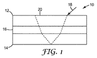
本発明の代表的実施形態の概略は図1に示されており、光学デバイス10は、第一光学部材12と、第二光学部材14と、これらの間に帯電防止層16と、を備える。この実施形態では、帯電防止層16は、第一光学部材12と第二光学部材14の両方と直接接触している。意図されている用途では、光は光線18により示されているように前面20に入射し、入射するとすぐに光は光学デバイス10により所望されるように操作される。
An outline of an exemplary embodiment of the present invention is shown in FIG. 1, and an
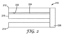
本発明の別の代表的実施形態の略図は図2に示され、ここで、光学デバイス210は、第一光学部材212と、第二光学部材214と、追加の接着層224により第一光学部材212の背面222に接着された帯電防止層216と、を備える。デバイス210は、所望の光学性能を達成するために所望される光学的に有効な配置で第一光学部材212と第二光学部材214とを支持する追加のフレーム226を更に含む。
A schematic diagram of another exemplary embodiment of the present invention is shown in FIG. 2, where the
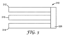
本発明の更に別の代表的実施形態の略図は図3に示されており、ここで、光学デバイス310は、第一光学部材312と、第二光学部材314と、これらの光学部材の間にどちらの光学部材にも接触せずに存在し、追加のフレーム326により所望の光学的に有効な配置で支持されている光学部材帯電防止層316と、を備える。
A schematic diagram of yet another exemplary embodiment of the present invention is shown in FIG. 3, where the
当業者であれば、好適な接着剤、もしあればフレーム構成要素、並びにもしあれば本発明による光学デバイスの他の構成要素を容易に選択することができるであろう。 One skilled in the art will readily be able to select a suitable adhesive, frame components, if any, and other components, if any, of the optical device according to the present invention.
本発明の光学デバイスで使用するための光学部材は、得られるデバイスの所望される光学性能に一部依存して、当業者により容易に選択することができる。本明細書で使用される光学フィルムは、例えば、ポリエステル系フィルムと称される場合もある、ポリエステルの実質的に平坦なシートなどの単層部材、あるいは、より特殊化した光学性能を提供する複雑に形成された構造特性を備える多層組立体であってもよい。例えば、第一光学部材及び第二光学部材は、独立して、光学ベースフィルム、多層光学フィルム、拡散反射偏光フィルム、プリズム状輝度上昇フィルム、プリズム状光学構造の配列、レンズ状光学構造の配列及びビーズ利得拡散フィルムからなる群から選択されてもよい。 The optical member for use in the optical device of the present invention can be readily selected by those skilled in the art depending in part on the desired optical performance of the resulting device. The optical film used herein is a single layer member, such as a substantially flat sheet of polyester, sometimes referred to as a polyester-based film, or a complex that provides more specialized optical performance. It may be a multi-layer assembly with structural characteristics formed in For example, the first optical member and the second optical member are independently an optical base film, a multilayer optical film, a diffuse reflection polarizing film, a prism-like brightness enhancement film, an arrangement of prism-like optical structures, an arrangement of lens-like optical structures, and It may be selected from the group consisting of bead gain diffusion films.
一部の実施形態では、光学部材の一方又は両方は、個別に、反射性偏光子(例えば、反射率を変える規則正しく繰り返す層を有するいわゆる多層光学フィルム又は「MOF」)、輝度上昇フィルム及び拡散反射偏光フィルム(様々な反射率の領域を持つ多層構造を有する「DRPF」と称される場合もある)からなる群から選択される。反応性偏光子の一代表例は、3M Company(St.Paul,MN)から市販され、米国特許第7,345,137号(Hebrinkら)に記載されているVIKUITI(商標)Dual Brightness Enhancement Film II(DBEF−II)である。好適なプリズム状輝度上昇フィルム(「BEF」と称される場合もある)も3Mから市販されており、例えば、米国特許第5,771,328号(Wortman et al.)、同第6,280,063号(Fong)及び同第6,354,709号(Campbellら)並びに米国特許出願公開第20090017256号(Huntら)に記載されている。光学部材として使用できる拡散反射偏光フィルムの代表例としては、米国特許第5,825,543号(Ouderkirkら)に開示されているものが挙げられる。本明細書での使用に好適な市販の光学フィルムの代表例としては、VIKUITI(商標)Dual Brightness Enhanced Film(DBEF)、VIKUITI(商標)Brightness Enhanced Film(BEF)、VIKUITI(商標)Diffuse Reflective Polarizer Film(DRPF)、VIKUITI(商標)Enhanced Specular Reflector(ESR)及びVIKUITI(商標)Advanced Polarizing Film(APF)が挙げられ、全て3M Companyから入手可能である。 In some embodiments, one or both of the optical members are individually reflective polarizers (eg, so-called multilayer optical films or “MOF” having regularly repeating layers that change reflectivity), brightness enhancement films, and diffuse reflection. Selected from the group consisting of polarizing films (sometimes referred to as “DRPF” having a multilayer structure with regions of varying reflectivity). One representative example of a reactive polarizer is the VIKUTI ™ Dual Brightness Enhancement Film II, which is commercially available from 3M Company (St. Paul, MN) and described in US Pat. No. 7,345,137 (Heblink et al.). (DBEF-II). Suitable prismatic brightness enhancement films (sometimes referred to as “BEF”) are also commercially available from 3M, for example, US Pat. No. 5,771,328 (Wortman et al.), 6,280. , 063 (Fong) and 6,354,709 (Campbell et al.) And US Patent Application Publication No. 20090017256 (Hunt et al.). Typical examples of the diffuse reflection polarizing film that can be used as the optical member include those disclosed in US Pat. No. 5,825,543 (Ouderkirk et al.). Representative examples of commercially available optical films suitable for use herein include VIKUTI (TM) Dual Brightness Enhanced Film (DBEF), VIKUTI (TM) Brightness Enhanced Film (BEF), and VIKUTIm (R) PVI (DRPF), VIKUTI ™ Enhanced Specular Reflector (ESR) and VIKUTI ™ Advanced Polarizing Film (APF), all available from 3M Company.
米国特許第5,175,030号及び同第5,183,597号(どちらもLuら)に記載のように、微細構造保有物品(例えば輝度上昇フィルム)は、(a)重合性組成物を調製する工程と、(b)マスターのキャビティーを満たすのにかろうじて十分な量でマスターネガ微細構造化成形表面上に重合性組成物を付着させる工程と、(c)予備成形されたベース(PETフィルムなど)とマスター(少なくとも一方は可撓性である)との間で重合性組成物のビーズを移動させることによりキャビティーを満たす工程と、(d)組成物を硬化させる工程と、を含む方法により作製可能である。マスターは、ニッケル、ニッケルメッキした銅若しくは黄銅のような金属製であってもよく、又は重合条件下で安定であって、好ましくは重合した材料をマスターからきれいに取り出すことができる表面エネルギーを有する、熱可塑性材料であってもよい。 As described in U.S. Pat. Nos. 5,175,030 and 5,183,597 (both Lu et al.), Microstructured articles (e.g., brightness enhancement films) are obtained from (a) a polymerizable composition. And (b) depositing the polymerizable composition on the master negative microstructured molding surface in an amount that is barely sufficient to fill the master cavity; and (c) a preformed base (PET). Filling the cavity by moving beads of the polymerizable composition between the film and the like (at least one of which is flexible), and (d) curing the composition. It can be produced by a method. The master may be made of metal, such as nickel, nickel-plated copper or brass, or is stable under polymerization conditions and preferably has a surface energy that allows the polymerized material to be removed cleanly from the master. It may be a thermoplastic material.
有用なベース材料としては、例えば、スチレン−アクリロニトリル、セルロースアセテートブチレート、セルロースアセテートプロピオネート、セルローストリアセテート、ポリエーテルスルホン、ポリメチルメタクリレート、ポリウレタン、ポリエステル、ポリカーボネート、ポリ塩化ビニル、ポリスチレン、ポリエチレンナフタレート、ナフタレンジカルボン酸系コポリマー又はブレンド、ポリシクロオレフィン、ポリイミド、及びガラスが挙げられる。所望により、ベース材料には、これらの材料の混合物又は組み合わせを含有させることができる。更に、ベースは多層であってもよいし、又は連続相の中に懸濁又は分散した分散成分を含有してもよい。 Useful base materials include, for example, styrene-acrylonitrile, cellulose acetate butyrate, cellulose acetate propionate, cellulose triacetate, polyethersulfone, polymethyl methacrylate, polyurethane, polyester, polycarbonate, polyvinyl chloride, polystyrene, polyethylene naphthalate. , Naphthalene dicarboxylic acid copolymers or blends, polycycloolefins, polyimides, and glasses. If desired, the base material can contain a mixture or combination of these materials. Further, the base may be multi-layered or may contain dispersed components suspended or dispersed in a continuous phase.
輝度上昇フィルムなどの微細構造保有製品の場合、好ましいベース材料の例には、ポリエチレンテレフタレート(PET)及びポリカーボネートが挙げられる。有用なPETフィルムの例としては、フォトグレードのポリエチレンテレフタレート及びMELINEX(商標)PET(DuPont Teijin Films(Hopewell,VA)から入手可能)が挙げられる。 In the case of microstructured products such as brightness enhancement films, examples of preferred base materials include polyethylene terephthalate (PET) and polycarbonate. Examples of useful PET films include photograde polyethylene terephthalate and MELINEX ™ PET (available from DuPont Teijin Films (Hopewell, Va.)).
いくつかのベース材料は、光学的に活性であり得、偏光材料として機能することができる。フィルムを通る光の偏光は、例えば通過光を選択的に吸収する二色偏光子を、フィルム材料に包含させることにより実現され得る。光の偏光はまた、配列雲母チップのような無機材料を組み込むことによって、又は、不連続相を連続フィルム中に分散させることによって(連続フィルム中に光変調液晶の液滴を分散させるなど)実現させることができる。代替手段として、異なる材料の微細層から偏光フィルムを調製することができる。フィルム内の材料は、例えば、フィルムの延伸、電場又は磁場の印加、及びコーティング技術のような方法を用いることによって、偏光配向に揃えることができる。 Some base materials can be optically active and can function as polarizing materials. Polarization of light through the film can be achieved, for example, by including in the film material a dichroic polarizer that selectively absorbs the passing light. Light polarization can also be achieved by incorporating inorganic materials such as aligned mica chips, or by dispersing discontinuous phases in a continuous film (such as dispersing light-modulated liquid crystal droplets in a continuous film). Can be made. As an alternative, polarizing films can be prepared from fine layers of different materials. The material in the film can be aligned to the polarization orientation, for example, by using methods such as stretching the film, applying an electric or magnetic field, and coating techniques.
偏光フィルムの例としては、米国特許第5,825,543号及び同第5,783,120号(両方ともOuderkirkら)に記載のものが挙げられる。これらの偏光フィルムを輝度上昇フィルムと組み合わせて使用することが米国特許第6,111,696号(Allenら)に記載されている。ベースとして使用できる偏光フィルムの他の例は、米国特許第5,882,774号(Jonzaら)に記載のフィルムである。 Examples of polarizing films include those described in US Pat. Nos. 5,825,543 and 5,783,120 (both to Ouderkirk et al.). The use of these polarizing films in combination with brightness enhancement films is described in US Pat. No. 6,111,696 (Allen et al.). Another example of a polarizing film that can be used as a base is the film described in US Pat. No. 5,882,774 (Jonza et al.).
有用な基材としては、全て3M Companyから入手可能なVIKUITI(商標)Dual Brightness Enhancement Film(DBEF)、VIKUITI(商標)Brightness Enhancement Film(BEF)、VIKUITI(商標)Diffuse Reflective Polarizer Film(DRPF)、VIKUITI(商標)Enhanced Specular Reflector(ESR)及びVIKUITI(商標)Advanced Polarizing Film(APF)として市場に出ている市販の光学フィルムが挙げられる。 Useful substrates include all VIKUITI ™ Dual Brightness Enhancement Film (DBEF), VIKUTI ™ Brightness Enhancement Film (BEF), VIKUITiP (DEF), which is available from 3M Company. (Trademark) Enhanced Optical Reflector (ESR) and VIKUTI (trademark) Advanced Polarizing Film (APF) are commercially available optical films.
ベースへの光学部材の付着を促進するために、ベースフィルム材料の1つ以上の表面に、場合により下地処理又は他の処理を施すことができる。ポリエステルベースフィルム層に特に好適なプライマーとしては、米国特許第5,427,835号(Morrisonら)に記載されているようなスルホポリエステルプライマーが挙げられる。プライマー層の厚さは、典型的には少なくとも20nmであり、一般的には、300nm以下から400nm以下である。 One or more surfaces of the base film material can optionally be pretreated or otherwise treated to promote the attachment of the optical member to the base. Particularly suitable primers for the polyester base film layer include sulfopolyester primers as described in US Pat. No. 5,427,835 (Morrison et al.). The thickness of the primer layer is typically at least 20 nm and is generally 300 nm or less to 400 nm or less.
光学部材は、任意の多数の有用なパターンを有することができる。これらのパターンには、規則的又は不規則的なプリズムパターンを含む。そのようなプリズムパターンは環状プリズムパターン、キューブコーナーパターン又は任意のその他のレンズ状微細構造であり得る。有用な微細構造は、輝度上昇フィルムとして使用するための全内部反射フィルムとして機能し得る、規則的プリズムパターンである。別の有用な微細構造は、反射フィルムとして使用するための再帰反射フィルム又は素子として作用できるコーナーキューブプリズムパターンである。別の有用な微細構造は、光学ディスプレイに使用するための光学回転フィルム又は光学回転素子として機能し得るプリズムパターンである。 The optical member can have any number of useful patterns. These patterns include regular or irregular prism patterns. Such prism patterns can be annular prism patterns, cube corner patterns or any other lenticular microstructure. A useful microstructure is a regular prism pattern that can function as a total internal reflection film for use as a brightness enhancement film. Another useful microstructure is a corner cube prism pattern that can act as a retroreflective film or element for use as a reflective film. Another useful microstructure is a prism pattern that can function as an optical rotating film or optical rotating element for use in an optical display.
重合化された微細構造化表面を有する1つの好ましい光学フィルムは、輝度上昇フィルムである。輝度上昇フィルムは、一般に、照明装置の軸上の輝き(本明細書で「輝度」と呼ばれる)を増強する。微細構造のトポグラフィーは、フィルム表面上に複数のプリズムがあるものであってよく、その結果、このフィルムの使用により、反射及び屈折を通じて光を転送することができる。プリズムの高さは1〜75マイクロメートルの範囲であるが、この範囲外の構造ももちろん使用することができる。ラップトップコンピュータ、時計などに見られるような光学ディスプレイ中で使用される場合、微細構造光学フィルムは、ディスプレイから散逸する光を、光学ディスプレイを貫通する垂直軸から所望の角度で配置される一対の平面内に制限することによって、光学ディスプレイの輝度を増大させることができる。結果として、許容範囲の外側に発散するはずだった光は、反射してディスプレイ内へ戻り、この光の一部は「再利用」され、ディスプレイから発散することのできる角度で微細構造フィルムに戻ることになる。この再利用は、ディスプレイに所望の輝度レベルを提供するために必要とされる電力消費量を低減することができることから、有用である。 One preferred optical film having a polymerized microstructured surface is a brightness enhancement film. The brightness enhancement film generally enhances the brightness on the axis of the lighting device (referred to herein as “luminance”). Microstructure topography may be a plurality of prisms on the film surface, so that the use of this film can transmit light through reflection and refraction. The height of the prism is in the range of 1 to 75 micrometers, but structures outside this range can of course be used. When used in an optical display such as found in laptop computers, watches, etc., a microstructured optical film is a pair of light that is dissipated from the display at a desired angle from a vertical axis that penetrates the optical display. By limiting to the plane, the brightness of the optical display can be increased. As a result, light that would have diverged outside the tolerance range would be reflected back into the display, and some of this light would be “reused” back to the microstructured film at an angle that could be diverged from the display. It will be. This reuse is useful because it can reduce the power consumption required to provide the desired brightness level for the display.
輝度上昇フィルムの微細構造化光学部材は、一般に、フィルムの長さ又は幅に沿って伸びる複数の平行な長手方向隆起部を含む。これらの隆起部は、複数個のプリズム先端から形成され得る。各プリズムは、第一ファセット及び第二ファセットを有する。プリズムは、プリズムが形成されている第一表面及び実質的に平ら又は平面でありかつ第一表面に対向する第二表面を有する、ベースの上に形成されている。直角プリズムとは、その頂角が、典型的には90°であることを意味する。しかしながら、この角度は、70°〜120°の範囲であってもよく、80°〜100°の範囲であってもよい。これらの先端は、先鋭形、丸形、又は平坦形若しくは切頭形とすることができる。例えば、隆起部は4〜7〜15マイクロメートルの範囲の半径に丸めることができる。プリズム頂点間の間隔(又はピッチ)は、5〜300マイクロメートルであることができる。プリズムは、米国特許第7,074,463号(Jonesら)に記載のもののように種々のパターンに調製することができる。 The microstructured optical member of a brightness enhancement film generally includes a plurality of parallel longitudinal ridges that extend along the length or width of the film. These ridges can be formed from a plurality of prism tips. Each prism has a first facet and a second facet. The prism is formed on a base having a first surface on which the prism is formed and a second surface that is substantially flat or planar and opposite the first surface. A right angle prism means that its apex angle is typically 90 °. However, this angle may be in the range of 70 ° to 120 °, and may be in the range of 80 ° to 100 °. These tips can be sharp, round, flat or truncated. For example, the ridges can be rounded to a radius in the range of 4-7-15 micrometers. The spacing (or pitch) between the prism vertices can be 5 to 300 micrometers. The prisms can be prepared in various patterns, such as those described in US Pat. No. 7,074,463 (Jones et al.).
輝度上昇フィルムの構造のピッチは、典型的には1ミリメートル以下、より好ましくは10マイクロメートル〜100マイクロメートル、更により好ましくは24マイクロメートル〜50マイクロメートルである。50マイクロメートルのピッチは、きわめて良好に機能することが判明している。好ましいピッチは、液晶ディスプレイのピクセルピッチ又はフィルムの一部の他の光学用途のパラメータに部分的に依存する。プリズムピッチは、モアレ干渉を最小化するのを補助するよう選択すべきである。 The pitch of the brightness enhancing film structure is typically 1 millimeter or less, more preferably 10 micrometers to 100 micrometers, and even more preferably 24 micrometers to 50 micrometers. A pitch of 50 micrometers has been found to work very well. The preferred pitch depends in part on the pixel pitch of the liquid crystal display or other optical application parameters of a portion of the film. The prism pitch should be chosen to help minimize moiré interference.
薄い輝度上昇フィルムを使用する本発明の光学デバイスでは、ピッチは、好ましくは10〜36マイクロメートル、より好ましくは17〜24マイクロメートルである。これは、好ましくは5〜18マイクロメートル、より好ましくは9〜12マイクロメートルのプリズム高さに相当する。プリズムファセットは同一である必要はなく、プリズムは互いに関して傾斜していてもよい。光学物品の全厚とプリズム高さとの関係は、変化してもよい。しかし、典型的には、輪郭のはっきりしたプリズムファセットを備えた比較的薄い光学部材を使用することが望ましい。ほぼ1ミル(20〜35マイクロメートル)の厚さを有する基材上の薄い輝度上昇フィルムの場合、全厚に対するプリズム高さの典型的な比率は、一般に、0.2〜0.4である。他の実施形態では、より厚いBEF材が使用され、例えば、BEF材は50マイクロメートルピッチ及び25マイクロメートル厚さを有する。 In the optical device of the present invention using a thin brightness enhancement film, the pitch is preferably 10 to 36 micrometers, more preferably 17 to 24 micrometers. This corresponds to a prism height of preferably 5-18 micrometers, more preferably 9-12 micrometers. The prism facets need not be identical and the prisms may be tilted with respect to each other. The relationship between the total thickness of the optical article and the prism height may vary. However, it is typically desirable to use a relatively thin optical member with a well-defined prism facet. For thin brightness enhancement films on substrates having a thickness of approximately 1 mil (20-35 micrometers), the typical ratio of prism height to total thickness is generally 0.2-0.4. . In other embodiments, a thicker BEF material is used, for example, the BEF material has a 50 micrometer pitch and a 25 micrometer thickness.
当業者であれば理解するように、本発明の光学デバイスは、上記代表例以外の他の種類の光学部材、あるいは、MOF、BEF又はDRPF材の他の実施形態を使用して作製してもよい。 As will be appreciated by those skilled in the art, the optical device of the present invention may be fabricated using other types of optical members other than the above representative examples, or other embodiments of MOF, BEF or DRPF materials. Good.
本明細書に記載の帯電防止構造体は、帯電防止剤を含む重合性樹脂組成物の重合反応生成物を含む。 The antistatic structure described in the present specification includes a polymerization reaction product of a polymerizable resin composition containing an antistatic agent.
様々な帯電防止剤が(「実施例」に記載の試験方法に従って測定したとき)2〜10秒の静電気減衰時間を提供することができるが、特定の種類及び量の帯電防止剤のみが2秒未満の静電気減衰時間を提供できることが判明した。好ましい帯電防止剤は、2、1又は0.1秒以下の静電気減衰時間を提供する。 Various antistatic agents can provide an electrostatic decay time of 2-10 seconds (when measured according to the test methods described in the "Examples"), but only certain types and amounts of antistatic agents are 2 seconds. It has been found that an electrostatic decay time of less than can be provided. Preferred antistatic agents provide static decay times of 2, 1 or 0.1 seconds or less.
微細構造又は微細構造化部材が帯電防止層上に配置され、帯電防止層が光透過性(例えば、ポリエステル)フィルム又は多層光学フィルムなどのベース層上に配置されている実施形態では、帯電防止層内の帯電防止剤の種類及び量も、重合性樹脂中のこれらの存在がベースフィルム層又は微細構造若しくは微細構造化部材との重合帯電防止層の接着を損なわないように選択される。このようにして得られる構造体全体は、(「実施例」に記載の試験方法に従って測定したとき)ベースフィルム層の少なくとも80%、85%又は90%に対してクロスハッチ引き剥がし粘着力を呈する。最も好ましい実施形態では、クロスハッチ粘着力は、95〜100%である。 In embodiments where the microstructure or microstructured member is disposed on an antistatic layer and the antistatic layer is disposed on a base layer such as a light transmissive (eg, polyester) film or a multilayer optical film, the antistatic layer The type and amount of the antistatic agent within are also selected so that their presence in the polymerizable resin does not impair the adhesion of the polymerized antistatic layer to the base film layer or the microstructure or microstructured member. The entire structure thus obtained exhibits a cross-hatch peel adhesion for at least 80%, 85% or 90% of the base film layer (when measured according to the test method described in “Examples”). . In the most preferred embodiment, the cross hatch adhesion is 95-100%.
帯電防止層
帯電防止層は、アニオンを有する重合性オニウム塩を少なくとも一種と、非オニウム重合性モノマー、オリゴマー又はポリマーを少なくとも一種との、反応生成物を含む。
Antistatic Layer The antistatic layer contains a reaction product of at least one polymerizable onium salt having an anion and at least one non-onium polymerizable monomer, oligomer or polymer.
好適なオニウム塩は、アンモニウム塩、スルホニウム塩、ホスホニウム塩、ピリジニウム塩及びイミダゾリウム塩からなる群から選択することができる。 Suitable onium salts can be selected from the group consisting of ammonium salts, sulfonium salts, phosphonium salts, pyridinium salts and imidazolium salts.
本発明での使用に好ましいオニウム塩は、下式を有する:
(R1)a−bG+[(CH2)qDR2]bX− (I)
式中、
各R1は、独立して、アルキル、脂環式、アリール、アルカリ環式、アルカリール、脂環式アルキル、アラリサイクリック(aralicyclic)又は脂環式アリール部分を含み、ここで、このような部分は、例えば、窒素、酸素又はイオウなどのヘテロ原子を1個以上含んでもよく、あるいは、リン又はハロゲンを含んでもよく(それゆえに有機フッ素性であり得る)、R1は環式又は芳香族であってもよく、環内にG+を含んでもよく、
Gは窒素、イオウ又はリンであり、
Gがイオウである場合にはaは3であり、Gが窒素又はリンである場合にはaは4であり、
Gがイオウである場合にはbは1〜3の整数であり、Gが窒素又はリンである場合にはbは1〜4の整数であり、
qは1〜4の整数であり、
Dは、酸素、イオウ又はNRであり、ここで、RはH又は炭素原子数1〜4個の低級アルキルであり、
R2は(メタ)アクリルであり、
X−は、アニオン、好ましくは有機アニオン、より好ましくは有機フッ素アニオンである。
Preferred onium salts for use in the present invention have the following formula:
(R 1 ) ab G + [(CH 2 ) q DR 2 ] b X − (I)
Where
Each R 1 independently comprises an alkyl, alicyclic, aryl, alkaline, alkaryl, alicyclic alkyl, aracyclic or alicyclic aryl moiety, where such The moiety may contain one or more heteroatoms such as, for example, nitrogen, oxygen or sulfur, or may contain phosphorus or halogen (hence may be organofluorine) and R 1 may be cyclic or aromatic Or may contain G + in the ring,
G is nitrogen, sulfur or phosphorus;
A is 3 when G is sulfur, a is 4 when G is nitrogen or phosphorus,
When G is sulfur, b is an integer of 1 to 3, and when G is nitrogen or phosphorus, b is an integer of 1 to 4,
q is an integer of 1 to 4,
D is oxygen, sulfur or NR, wherein R is H or lower alkyl of 1 to 4 carbon atoms;
R 2 is (meth) acryl,
X − is an anion, preferably an organic anion, more preferably an organic fluorine anion.
本開示を通して、「アクリル」の任意の誘導体の前での「(メタ)」の使用は、「アクリル又はメタアクリル」を意味するものとして理解される。 Throughout this disclosure, the use of “(meth)” in front of any derivative of “acryl” is understood to mean “acryl or methacryl”.
一部の実施形態では、G+が環内に含まれる場合、オニウム塩は下式のうちの1つを有する: In some embodiments, when G + is included in the ring, the onium salt has one of the following formulas:

オニウム塩は、層中に、1〜99%、好ましくは10〜60%、より好ましくは30〜50%の重量百分率で存在し得る。アクリル官能性オニウムは、より速く強力な硬化を呈することからメタクリルオニウムよりも好ましい。 The onium salt may be present in the layer in a weight percentage of 1 to 99%, preferably 10 to 60%, more preferably 30 to 50%. Acrylic functional oniums are preferred over methacrylonium because they exhibit faster and stronger cure.
本明細書で有用なアニオンの代表例としては、アルキル硫酸塩、メタンスルホン酸塩、トシル酸塩、有機フッ素化合物、無機フッ素化合物及びハロゲン化物が挙げられる。 Representative examples of anions useful herein include alkyl sulfates, methanesulfonates, tosylates, organic fluorine compounds, inorganic fluorine compounds, and halides.
最も好ましくは、アニオンは、フッ素化学アニオンである。本明細書での使用に好適な有機フッ素アニオンとしては、米国特許第6,924,329号(Klunら)の8段2〜65行に記載のものが挙げられる。有機フッ素イオンは、非オニウム重合性モノマー、オリゴマー又はポリマーとのオニウム塩の、より大きな溶解度特性及び適合性を提供する。これは、良好な透明性、並びに、得られる層の多電防止性能を向上できる良好なイオン移動度を有する層を提供する上で重要である。一部の代表例としては、−C(SO2CF3)3、−O3SCF3、−O3SC4F9及び−N(SO2CF3)2が挙げられる。入手性及びコストに起因して、多くの場合以下のものが好ましい:−O3SCF3、−O3SC4F9及び−N(SO2CF3)2。典型的には、一部の代替物よりも広範囲の溶解度を提供し、これを含有する組成物の調製及び使用を容易にすることから、−N(SO2CF3)2が最も好ましい。 Most preferably, the anion is a fluorine chemical anion. Organofluorine anions suitable for use herein include those described in US Pat. No. 6,924,329 (Klun et al.), 8th column, lines 2 to 65. Organic fluoride ions provide greater solubility characteristics and compatibility of onium salts with non-onium polymerizable monomers, oligomers or polymers. This is important in providing a layer with good transparency, as well as good ion mobility that can improve the multi-electric performance of the resulting layer. As some typical examples, -C (SO 2 CF 3) 3, -O 3 SCF 3, -O 3 SC 4 F 9 and -N (SO 2 CF 3) 2 and the like. Due to availability and cost, the followings often preferred: -O 3 SCF 3, -O 3 SC 4 F 9 and -N (SO 2 CF 3) 2 . Typically, to provide a wide range of solubility than some alternatives, it facilitates the preparation and use of compositions containing them, -N (SO 2 CF 3) 2 is most preferable.
非オニウム重合性モノマー、オリゴマー又はポリマーは、光学フィルムの性能の鍵である。これらは、オニウム塩と共に、フィルムの静電気減衰、その曇り及び透明度、その凝集強度並びにその層間接着などの帯電防止光学フィルムの鍵となる特性を制御する。 Non-onium polymerizable monomers, oligomers or polymers are key to the performance of the optical film. These, together with the onium salt, control key properties of the antistatic optical film such as static decay of the film, its haze and transparency, its cohesive strength and its interlayer adhesion.
オニウム塩、重合性シリコーン及び/又はペルフルオロポリエーテル内容物、並びにもしあれば他の構成要素は、これらが混合され重合して透明なフィルムを形成するという点で、相溶性であるべきである。 The onium salt, polymerizable silicone and / or perfluoropolyether content, and other components, if any, should be compatible in that they are mixed and polymerized to form a transparent film.
一部の実施形態では、帯電防止層は、以下の方法により光学層上に形成される:(1)(a)上記に記載のような少なくとも一種の重合性オニウム塩と、(b)上記に記載のような少なくとも一種の非オニウム重合性シリコーン又はペルフルオロポリエーテル部分含有モノマー、オリゴマー又はポリマーと、(c)少なくとも一種の非シリコーン、非ペルフルオロエーテルモノマー、オリゴマー又はポリマーと、を含む液体コーティング組成物を提供すること、(2)光学層の表面に液体コーティング組成物を適用すること、並びに(3)液体コーティング組成物をその場で硬化させて、光学層の表面上に帯電防止層を形成すること。他の実施形態では、帯電防止層は、例えば、ポリエステルフィルムといった、基材フィルムの一方の側の上に形成され、その反対側は続いて光学フィルムの表面上に配置され、例えば、積層により又は接着剤で接着され、あるいは、機械的手段で適所に保持される。 In some embodiments, the antistatic layer is formed on the optical layer by the following method: (1) (a) at least one polymerizable onium salt as described above; and (b) above. A liquid coating composition comprising at least one non-onium polymerizable silicone or perfluoropolyether moiety-containing monomer, oligomer or polymer as described, and (c) at least one non-silicone, non-perfluoroether monomer, oligomer or polymer. (2) applying a liquid coating composition to the surface of the optical layer; and (3) curing the liquid coating composition in situ to form an antistatic layer on the surface of the optical layer. about. In other embodiments, the antistatic layer is formed on one side of a substrate film, such as a polyester film, and the opposite side is subsequently disposed on the surface of the optical film, for example, by lamination or Glued with an adhesive or held in place by mechanical means.
本明細書に開示される「実施例」は、帯電防止層のTg及び本発明の光学デバイスにより呈される静電気減衰に関するデータを提供する。 The “Examples” disclosed herein provide data regarding the antistatic layer T g and the electrostatic decay exhibited by the optical device of the present invention.
硬化した帯電防止層のTgは、好ましくは50℃未満、より好ましくは40℃未満、更により好ましくは30℃未満、更により好ましくは20℃未満、更により好ましくは10℃未満、最も好ましくは0℃未満である。この理論に束縛されるものではないが、イオン移動度は所望の帯電防止性を提供するのに必要とされると考えられる。 The T g of the cured antistatic layer is preferably less than 50 ° C., more preferably less than 40 ° C., even more preferably less than 30 ° C., even more preferably less than 20 ° C., even more preferably less than 10 ° C., most preferably It is less than 0 ° C. Without being bound by this theory, it is believed that ion mobility is required to provide the desired antistatic properties.
非オニウム重合性モノマー、オリゴマー又はポリマーは、加工及びコーティングに適合している透明で均質な溶液を提供すべく、オニウム塩と相溶性であるように注意深く選択されなければならない。意図されるコーティング配合物が有意に非相溶性である場合には、構成要素は2つの液相に階層化してしまうか、又は固体沈殿を形成して混合物をコーティングプロセスにおいて操作するのに不適切なものにしてしまうか、並びに/又は、曇り及び不均一な硬化済みコーティングを生じてしまうかする可能性がある。 The non-onium polymerizable monomer, oligomer or polymer must be carefully selected to be compatible with the onium salt to provide a clear and homogeneous solution that is compatible with processing and coating. If the intended coating formulation is significantly incompatible, the component will stratify into two liquid phases or form a solid precipitate that is inappropriate for operating the mixture in the coating process And / or can result in haze and non-uniform cured coatings.
帯電防止層用の材料の選択は、層が密着している場合に、第一光学部材及び第二光学部材に対する帯電防止層の接着に影響する。この接着要件は、特に光学ディスプレイフィルムにおいて重大であり、この構造体は、光学部材と介在する帯電防止コーティングとの間に接着不良を生じることなくバックライト産業の耐久要件を持ちこたえる必要がある。 The selection of the material for the antistatic layer affects the adhesion of the antistatic layer to the first optical member and the second optical member when the layers are in close contact. This adhesion requirement is particularly critical in optical display films, and this structure needs to withstand the durability requirements of the backlight industry without causing poor adhesion between the optical member and the intervening antistatic coating.
非オニウム重合性モノマー、オリゴマー又はポリマーは、硬化した帯電防止層の十分な凝集強度を有する層を提供するために注意深く選択しなければならない。凝集強度は、上記のように仕上がった光学構造体の耐久性のために重要なだけでなく、帯電防止配合物のコーティング及び硬化の成功にとっても決定的である。例えば、選択される帯電防止配合物を、微細組織の造成のための成形型に対して流延して硬化させる場合には、複製表面からの硬化コーティングの有効で包括的な剥離は、コーティングの凝集強度に強く依存する。これは特に、電荷減衰の割増及び更なる帯電防止性能が必要とされる、Tgがより低い(機械的に軟らかい)配合物に対しての課題である。 The non-onium polymerizable monomer, oligomer or polymer must be carefully selected to provide a layer with sufficient cohesive strength of the cured antistatic layer. The cohesive strength is not only critical for the durability of the optical structure finished as described above, but is also critical to the successful coating and curing of the antistatic formulation. For example, when the selected antistatic formulation is cast and cured against a mold for microstructuring, an effective and comprehensive release of the cured coating from the replicated surface is It strongly depends on the cohesive strength. This is particularly premium and additional antistatic performance of charge decay is required is an issue with respect to T g is lower (mechanically soft) formulations.
有用な非オニウム重合性モノマー、オリゴマー又はポリマーとしては、例えば、以下からなる群から選択されるポリ(メタ)アクリルモノマーを挙げてもよい:
(a)モノ(メタ)アクリル含有化合物、例えば、フェノキシエチルアクリレート、エトキシル化フェノキシエチルアクリレート、2−エトキシエトキシエチルアクリレート、エトキシル化テトラヒドロフルフラールアクリレート及びカプロラクトンアクリレート;
(b)ジ(メタ)アクリル含有化合物、例えば、1,3−ブチレングリコールジアクリレート、1,4−ブタンジオールジアクリレート、1,6−ヘキサンジオールジアクリレート、1,6−ヘキサンジオールモノアクリレートモノメタクリレート、エチレングリコールジアクリレート、アルコキシル化脂肪族30ジアクリレート、アルコキシル化シクロヘキサンジメタノールジアクリレート、アルコキシル化ヘキサンジオール26ジアクリレート、アルコキシル化ネオペンチルグリコールジアクリレート、カプロラクトン変性ネオペンチルグリコールヒドロキシピバリン酸ジアクリレート、カプロラクトン変性ネオペンチルグリコールヒドロキシピバリン酸ジアクリレート、シクロヘキサンジメタノールジアクリレート、ジエチレングリコールジアクリレート、ジプロピレングリコールジアクリレート、エトキシル化(10)ビスフェノールAジアクリレート、エトキシル化(3)ビスフェノールAジアクリレート、エトキシル化(30)ビスフェノールAジアクリレート、エトキシル化(4)ビスフェノールAジアクリレート、ヒドロキシピバラルデヒド変性トリメチロールプロパンジアクリレート、ネオペンチルグリコールジアクリレート、ポリエチレングリコール(200)ジアクリレート、ポリエチレングリコール(400)ジアクリレート、ポリエチレングリコール(600)ジアクリレート、プロポキシル化ネオペンチルグリコールジアクリレート、テトラエチレングリコールジアクリレート、トリシクロデカンジメタノールジアクリレート、トリエチレングリコール10ジアクリレート、トリプロピレングリコールジアクリレート;
(c)トリ(メタ)アクリル含有化合物、例えば、グリセロールトリアクリレート、トリメチロールプロパントリアクリレート、ペンタエリスリトールトリアクリレート、エトキシル化トリアクリレート(例えば、エトキシル化(3)トリメチロールプロパントリアクリレート、エトキシル化(6)トリメチロールプロパントリアクリレート、エトキシル化(9)トリメチロールプロパントリアクリレート、エトキシル化(20)トリメチロールプロパントリアクリレート)、プロポキシル化トリアクリレート(例えば、プロポキシル化(3)グリセリル15トリアクリレート、プロポキシル化(5.5)グリセリルトリアクリレート、プロポキシル化(3)トリメチロールプロパントリアクリレート、プロポキシル化(6)トリメチロールプロパントリアクリレート)、トリメチロールプロパントリアクリレート、トリス(2−ヒドロキシエチル)イソシアヌレートトリアクリレート;
(d)高官能価の(メタ)アクリル含有化合物、例えば、ペンタエリスリトールテトラアクリレート、ジトリメチロールプロパンテトラアクリレート、ジペンタエリスリトールペンタアクリレート、エトキシル化(4)ペンタエリスリトールテトラアクリレート、カプロラクトン20変性ジペンタエリスリトールヘキサアクリレート;
(e)オリゴマーの(メタ)アクリル含有化合物、例えば、ウレタンアクリレート、ポリエステルアクリレート、エポキシアクリレート;以上のポリアクリルアミド類似体;並びに
(f)これらの組み合わせ。
Useful non-onium polymerizable monomers, oligomers or polymers may include, for example, poly (meth) acrylic monomers selected from the group consisting of:
(A) mono (meth) acryl-containing compounds such as phenoxyethyl acrylate, ethoxylated phenoxyethyl acrylate, 2-ethoxyethoxyethyl acrylate, ethoxylated tetrahydrofurfural acrylate and caprolactone acrylate;
(B) Di (meth) acryl-containing compounds such as 1,3-butylene glycol diacrylate, 1,4-butanediol diacrylate, 1,6-hexanediol diacrylate, 1,6-hexanediol monoacrylate monomethacrylate , Ethylene glycol diacrylate, alkoxylated aliphatic 30 diacrylate, alkoxylated cyclohexanedimethanol diacrylate, alkoxylated hexanediol 26 diacrylate, alkoxylated neopentyl glycol diacrylate, caprolactone-modified neopentyl glycol hydroxypivalic acid diacrylate, caprolactone Modified neopentyl glycol hydroxypivalic acid diacrylate, cyclohexanedimethanol diacrylate, diethyleneglycol Diacrylate, dipropylene glycol diacrylate, ethoxylated (10) bisphenol A diacrylate, ethoxylated (3) bisphenol A diacrylate, ethoxylated (30) bisphenol A diacrylate, ethoxylated (4) bisphenol A diacrylate, hydroxy Pivalaraldehyde modified trimethylolpropane diacrylate, neopentyl glycol diacrylate, polyethylene glycol (200) diacrylate, polyethylene glycol (400) diacrylate, polyethylene glycol (600) diacrylate, propoxylated neopentyl glycol diacrylate, tetra Ethylene glycol diacrylate, tricyclodecane dimethanol diacrylate, triethyleneglycol 10 diacrylate, tripropylene glycol diacrylate;
(C) Tri (meth) acryl-containing compounds such as glycerol triacrylate, trimethylolpropane triacrylate, pentaerythritol triacrylate, ethoxylated triacrylate (eg ethoxylated (3) trimethylolpropane triacrylate, ethoxylated (6 ) Trimethylolpropane triacrylate, ethoxylated (9) trimethylolpropane triacrylate, ethoxylated (20) trimethylolpropane triacrylate), propoxylated triacrylate (eg propoxylated (3) glyceryl 15 triacrylate, propoxy (5.5) Glyceryl triacrylate, propoxylated (3) trimethylolpropane triacrylate, propoxylated (6) trimethylol B pan triacrylate), trimethylolpropane triacrylate, tris (2-hydroxyethyl) isocyanurate triacrylate;
(D) High functionality (meth) acryl-containing compounds such as pentaerythritol tetraacrylate, ditrimethylolpropane tetraacrylate, dipentaerythritol pentaacrylate, ethoxylated (4) pentaerythritol tetraacrylate,
(E) oligomeric (meth) acryl-containing compounds such as urethane acrylates, polyester acrylates, epoxy acrylates; polyacrylamide analogues as described above; and (f) combinations thereof.
このような化合物は、例えば、Sartomer Company(Exton,Pennsylvania)、UCB Chemicals Corporation(Smyrna,Georgia)、Cytec Corporation(Smyrna,Georgia)、Cognis Performance Chemicals UK(South Hampton,UK)及びAldrich Chemical Company(Milwaukee,Wisconsin)などの業者から広く入手可能である。追加の有用な(メタ)アクリレート材料には、例えば、米国特許第4,262,072号(Wendlingら)に記載されているようなヒダントイン部分含有ポリ(メタ)アクリレートが挙げられる。 Such compounds are, for example, Sartomer Company (Exton, Pennsylvania), UCB Chemicals Corporation (Smyrna, Georgia), Cytec Corporation (Smyrna, Georgia), Cognis Performance Chemicals UK (South Hampton, UK) and Aldrich Chemical Company (Milwaukee, Widely available from vendors such as Wisconsin). Additional useful (meth) acrylate materials include, for example, hydantoin moiety-containing poly (meth) acrylates as described in US Pat. No. 4,262,072 (Wendling et al.).
オニウム塩及び重合性非オニウム内容物は、これらが混合され及び重合して透明なフィルムを形成する点で、相溶性であるべきである。 The onium salt and polymerizable non-onium content should be compatible in that they are mixed and polymerized to form a transparent film.
多くの用途では、得られる硬化コーティング層の少なくとも一表面が完全に滑らかではなく、むしろ微細組織化された表面及び/又は艶消し仕上げを有するように、本発明の帯電防止コーティングを適用することが有益であり得る。このように、帯電防止層はまた、例えば、引っかき傷などの物理的欠陥、並びに、モアレ及び色斑などの望ましくない光学効果を光学マスキング及び/又は除去するといった、追加的な目的を果たし得る。 For many applications, it is possible to apply the antistatic coating of the present invention so that at least one surface of the resulting cured coating layer is not completely smooth, but rather has a finely textured surface and / or a matte finish. Can be beneficial. Thus, the antistatic layer may also serve additional purposes such as optical masking and / or removal of physical defects such as scratches, and undesirable optical effects such as moire and color spots.
このような表面を製造する一方法は、微細構造化成形型に対合させて帯電防止層を成形することを伴う。代表例は、PCT出願番号第US2010/036018号(Aronsonら)及び第US2010/045118号(Yapelら)に開示されている。成形型の中に機械加工された微細構造は、成形型に対して流延された最終硬化コーティングの表面上に複製される。 One method of producing such a surface involves molding an antistatic layer against a microstructured mold. Representative examples are disclosed in PCT Application Nos. US2010 / 036018 (Aronson et al.) And US2010 / 045118 (Yapel et al.). The microstructure machined into the mold is replicated on the surface of the final cured coating cast against the mold.
微細構造は、特定の用途において望ましい任意の種類の微細構造であってよい。特定の場合では、微細構造はくぼみ又は凹部であってもよい。特定の場合では、微細構造は突起部であってもよい。特定の場合では、微細構造は規則的なパターンを形成する。特定の場合では、微細構造は不規則なパターンを形成する。特定の場合では、微細構造は一見ランダムに見える疑似ランダムパターンを形成する。一般的に、微細構造は任意の高さ及び任意の高さの分布を有し得る。 The microstructure can be any type of microstructure desired in a particular application. In certain cases, the microstructure may be a depression or a recess. In certain cases, the microstructure may be a protrusion. In certain cases, the microstructure forms a regular pattern. In certain cases, the microstructure forms an irregular pattern. In certain cases, the microstructure forms a pseudo-random pattern that appears to be random. In general, the microstructure can have any height and any height distribution.
PCT公開番号第US2010/036018号及び第US2010/045118号に開示されているように、所与の用途に有用な特定の利点は、ある閾値寸法よりも大きな勾配規模を有する非平坦な表面の部分を制御することにより、及び/あるいは、微細構造が、ある閾値以下である半値半幅(HWHM)を有する勾配分布を有する又はその値がある好ましい範囲にあるように微細構造を制御することにより、得ることができる。 As disclosed in PCT Publication Nos. US2010 / 036018 and US2010 / 045118, a particular advantage useful for a given application is the portion of a non-planar surface having a gradient magnitude greater than a certain threshold dimension. And / or by controlling the microstructure so that the microstructure has a gradient distribution with a half-width at half maximum (HWHM) that is less than or equal to a certain threshold, or that value is within a certain preferred range. be able to.
このような表面を製造する別の方法は、PCT出願番号第WO2009/079275号(Aronsonら)に教示されているように、成形型上で微細構造を成形するために金属の電着にかける、成形型に対合させて帯電防止層を成形することを伴う。成形型は、電着前にその上に一部の既に機械加工された微細構造を有してもよく、有さなくてもよい。この付着プロセスは、成形型上に隆起領域を作製し、これが今度は、成形型に対して流延された硬化コーティングにおいてくぼみを作製する。 Another method of producing such a surface is to subject the metal to electrodeposition to form a microstructure on a mold, as taught in PCT Application No. WO 2009/079275 (Aronson et al.). This involves forming an antistatic layer by mating with a mold. The mold may or may not have some already machined microstructures thereon prior to electrodeposition. This deposition process creates a raised area on the mold, which in turn creates indentations in the cured coating cast against the mold.
くぼみの形状及び寸法は、ロール成形型上に電気メッキされた金属のタイプに依存して様々である。くぼみの形状及び寸法は、ロール上にメッキされた金属構造の形状及び寸法の逆である。このような形状としては、孔、半球、「輪郭がギザギザの」谷部分、「クレータ」及びカリフラワ表面に似たものが挙げられる。くぼみは互いの内側に重なり合ってもよく、あるいは互いに離れていてもよい。くぼみの寸法すなわち最大直径の範囲は、これらの最大直径にて0.5マイクロメートル〜125マイクロメートルであり得る。典型的な範囲は、0.5〜15マイクロメートルである。くぼみの面積の範囲は、0.01〜1100平方マイクロメートルであり得る。深さの範囲は、0.2〜20マイクロメートルであり得る。 The shape and size of the recess varies depending on the type of metal electroplated on the roll mold. The shape and size of the recess is the inverse of the shape and size of the metal structure plated on the roll. Such shapes include holes, hemispheres, “rough outlines” valleys, “craters” and those that resemble cauliflower surfaces. The indents may overlap each other or may be separated from each other. The size of the indentation or maximum diameter range can be from 0.5 micrometers to 125 micrometers at these maximum diameters. A typical range is 0.5 to 15 micrometers. The range of the indentation area can be from 0.01 to 1100 square micrometers. The depth range can be 0.2 to 20 micrometers.
微細構造化表面上にくぼみを形成するために、一実施形態では、微細構造化ロールを電気メッキプロセスにかける。金属は、ロールの微細構造化表面上に不均一に融合し、突起を形成する。光学フィルムの微細構造化表面は、ロールの微細構造化表面に関して孔又は縦穴などを複製する。電気メッキプロセスを介して微細構造化ロール上に付着した金属構造の寸法及び密度は、電流密度、ロール面速度及びメッキ時間により決定される。電気メッキプロセスで使用される金属塩のタイプは、付着した金属構造の形状を決定し、これにより、微細構造化表面上のくぼみの形状を決定する。微細構造化ロール上に付着する金属構造の位置及び付着は、ランダムである。 To form a depression on the microstructured surface, in one embodiment, the microstructured roll is subjected to an electroplating process. The metal fuses non-uniformly on the microstructured surface of the roll and forms protrusions. The microstructured surface of the optical film replicates holes or vertical holes or the like with respect to the microstructured surface of the roll. The size and density of the metal structure deposited on the microstructured roll through the electroplating process is determined by the current density, roll face speed and plating time. The type of metal salt used in the electroplating process determines the shape of the deposited metal structure, thereby determining the shape of the depression on the microstructured surface. The location and deposition of the metal structure that deposits on the microstructured roll is random.
このような表面を製造する更に別の方法は、米国特許出願公開第2009/0029054号(Yapelら)に教示されているように模様がコーティング上に単純に押し付けられ、その場で硬化できるようなやり方で、円滑に適用された後、コーティングを硬化させるプロセスを取り扱うことを伴う。 Yet another method of producing such a surface is such that the pattern can simply be pressed onto the coating and cured in situ as taught in US 2009/0029054 (Yapel et al.). In a manner, it involves handling the process of curing the coating after it has been applied smoothly.
基材上に配置されたコーティング可能な材料を含むコーティングされた基材は、コーティングされた材料の粘度を初期粘度から第二粘度へ変化させ、次に、コーティングの表面を少なくとも一つの表面側のローラーに接触させ、艶消し仕上げを付与し、コーティング可能な材料を場合により更に硬化させて仕上げコーティングフィルムを提供するようなやり方で、処理される。 A coated substrate comprising a coatable material disposed on a substrate changes the viscosity of the coated material from an initial viscosity to a second viscosity, and then the surface of the coating is at least one surface side It is processed in such a manner as to contact the roller, impart a matte finish, and optionally further cure the coatable material to provide a finished coating film.
コーティング可能な材料は、基材上に適用(例えば、コーティング)されて、コーティングされた表面を提供する。コーティング可能な材料は、基材上を運ばれ、処理されて、コーティング可能な材料の粘度を第一又は初期粘度から第二粘度に変化させる。一部の実施形態では、第一粘度は第二粘度よりも低く、そのため、コーティング可能な材料は、増粘又は部分的に硬化させることにより変化する。一部の実施形態では、コーティング可能な材料は、第二粘度よりも高い初期粘度を有してもよく、そのため、コーティング可能な材料の粘度を変化させることは、コーティング可能な材料の少なくともいくらかの軟化を必要とし得る。コーティング可能な材料の粘度が一度第二粘度になると、その後、材料は、表面側の圧力にかけられて、その上に艶消し仕上げを付与する。艶消し仕上げにより、コーティング可能な材料は、場合により、更に硬化、硬質化又は固体化し得、得られるフィルムは、例えば、切断ステーションなどの別の加工ステーション又は巻き上げロールに運ばれ得る。高価な成形型は、艶消し仕上げを付与するのに必要とされない。 The coatable material is applied (eg, coated) onto the substrate to provide a coated surface. The coatable material is transported over the substrate and processed to change the viscosity of the coatable material from a first or initial viscosity to a second viscosity. In some embodiments, the first viscosity is lower than the second viscosity, so that the coatable material is changed by thickening or partially curing. In some embodiments, the coatable material may have an initial viscosity that is higher than the second viscosity, so that changing the viscosity of the coatable material is at least some of the coatable material. Softening may be required. Once the coatable material has a second viscosity, the material is then subjected to surface side pressure to provide a matte finish thereon. With a matte finish, the coatable material can optionally be further cured, hardened or solidified, and the resulting film can be conveyed to another processing station, such as a cutting station or a winding roll. Expensive molds are not required to provide a matte finish.
このような表面を製造する更に別の方法は、その基材に適用されるコーティング中にビーズを包含させることを伴う。多相コーティングは、表面のコーティング中に又はコーティングのバルク内に組み込まれた不混和性材料、例えば、コーティング中のポリメチルメタクリレートビーズなどの粒子の同伴から生じる艶消し表面構造を有することができる。一部の実施形態では、コーティングのバルクとは異なる屈折率を有する粒子を、艶消し表面の生成を必要とせずに所望の曇り特性を付与するために、使用することができる。有用な粒子は任意の形状を有してもよいが、典型的に好ましい粒子形状は、多くの場合、球形又は楕円形ビーズの形状である。好ましい粒径は、通常、0.1マイクロメートル〜20マイクロメートルの平均直径である。粒子は、コーティングと適合する任意の材料から製造することができる。粒子に好適な材料の一部の代表例としては、ポリメチルメタクリレート、ポリブチルメタクリレート、ポリスチレン、ポリウレタン、ポリアミド、ポリシリコーン及びシリカが挙げられる。有用な粒子は、ガンツ化成株式会社、積水化成品工業株式会社及び綜研化学株式会社(全て日本)から入手することができる。 Yet another method of producing such a surface involves the inclusion of beads in a coating applied to the substrate. Multiphase coatings can have a matte surface structure resulting from the entrainment of particles such as immiscible materials, eg polymethylmethacrylate beads, in the coating or incorporated into the bulk of the coating. In some embodiments, particles having a refractive index different from the bulk of the coating can be used to impart the desired haze characteristics without the need for a matte surface. Useful particles may have any shape, but typically preferred particle shapes are often spherical or elliptical bead shapes. The preferred particle size is usually an average diameter of 0.1 micrometers to 20 micrometers. The particles can be made from any material compatible with the coating. Some representative examples of suitable materials for the particles include polymethyl methacrylate, polybutyl methacrylate, polystyrene, polyurethane, polyamide, polysilicon, and silica. Useful particles can be obtained from Gantz Kasei Co., Ltd., Sekisui Kasei Kogyo Co., Ltd. and Soken Chemical Co., Ltd. (all in Japan).
帯電防止層に表面微細構造又は艶消し仕上げを提供するこれらの方法は、光学デバイス中で色斑又はカラーバンディングを低減するのに特に有効であり得る。これは、微細構造化表面又は艶消し仕上げを有する帯電防止層が続いて別の光学フィルム、特にマイクロプリズム層で上からコーティングされる場合に、特に当てはまる。 These methods of providing a surface microstructure or matte finish to the antistatic layer can be particularly effective in reducing color spots or color banding in optical devices. This is particularly true when an antistatic layer with a microstructured surface or matte finish is subsequently coated from above with another optical film, in particular a microprism layer.
米国特許出願公開第2007/0115407号(Richardら)は、カラーバンディングの問題、並びに、例えば、本発明の硬化した帯電防止層上の微細構造化表面又は艶消し仕上げにより提供されるカラーバンディングを除去する上での光拡散の役割について述べている。 US Patent Application Publication No. 2007/0115407 (Richard et al.) Removes the problem of color banding, as well as color banding provided, for example, by the microstructured surface or matte finish on the cured antistatic layer of the present invention. Describes the role of light diffusion in
本発明は、以下の実施例を参照しながら更に説明されるが、ここで、特に示さない限り、量は重量部で表される。 The invention will be further described with reference to the following examples, in which amounts are expressed in parts by weight unless otherwise indicated.
試験方法
実施例では以下の方法を使用した。
Test Method The following method was used in the examples.
帯電防止性能についての電荷減衰:平均静電荷減衰は、以下の方法を使用して、フィルムサンプルについて決定した。試験材料のシートを12cm×15cmサンプルに切り出し、23℃〜27℃の公称室温(「RT」)にて44%〜50%の相対湿度(「RH」)で少なくとも12時間にわたって状態調整した。ETS(商標)Model 406D Static Decay Test Unit(Electro−Tech Systems,Inc.(Glenside,PA)製)を用い、Federal Test Method Standard 10113,Method 4046,「Antistatic Properties of Materials」として以前は知られていたMIL−STD 3010,Method 4046に従う12時間の前条件付けで使用したものと同じ温度及び湿度条件下にて静電荷拡散時間を測定した。この装置を使用して、高圧(5000ボルト)を用い、平坦な試験材料の表面上に初期静電荷(平均誘導静電荷)を誘導し、電場計を使用して、電荷減衰を観察した。5000ボルト誘導の付加により誘導された実際の電荷を記録した。次に、電荷が初期誘導電荷の10パーセントに減衰するのに必要とされた時間を記録した。これが静電荷拡散時間である。静電荷拡散時間が短いほど、試験材料の帯電防止性能は良好である。本明細書内の静電荷拡散時間の全報告値は、少なくとも6個の別個の測定値の平均(平均電荷減衰)を取ることで決定した。これらの測定値のうちの少なくとも3個は正の+5kV印加電圧を用いて測定したものであり、これらの測定値のうちの少なくとも3個は負の−5kV印加電圧を用いて測定したものである。試験したサンプルが誘導された5kV電位の少なくとも80%(すなわち、4000ボルト)の電荷を受容しなかった場合、帯電防止性であるとはみなさず、表記「wnc」(荷電しない)を割り当てた。 Charge decay for antistatic performance: The average electrostatic charge decay was determined for film samples using the following method. Sheets of test material were cut into 12 cm x 15 cm samples and conditioned for at least 12 hours at a nominal room temperature ("RT") of 23 [deg.] C to 27 [deg.] C and 44% to 50% relative humidity ("RH"). The ETS (TM) Model 406D Static Decay Test Unit (from Electro-Tech Systems, Inc. (Glenside, PA)) was used as a Federal Test Method Standard 10113, Messard Standard 10106, Method The static charge diffusion time was measured under the same temperature and humidity conditions used in the 12 hour preconditioning according to MIL-STD 3010, Method 4046. Using this apparatus, high voltage (5000 volts) was used to induce an initial electrostatic charge (average induced electrostatic charge) on the surface of the flat test material, and charge decay was observed using an electrometer. The actual charge induced by the addition of 5000 volt induction was recorded. The time required for the charge to decay to 10 percent of the initial induced charge was then recorded. This is the electrostatic charge diffusion time. The shorter the electrostatic charge diffusion time, the better the antistatic performance of the test material. All reported values of electrostatic charge diffusion time within this specification were determined by taking an average (average charge decay) of at least 6 separate measurements. At least three of these measured values were measured using a positive +5 kV applied voltage, and at least three of these measured values were measured using a negative -5 kV applied voltage. . If the tested sample did not accept a charge of at least 80% of the induced 5 kV potential (ie 4000 volts), it was not considered antistatic and was assigned the designation “wnc” (not charged).
ガラス転移温度の示差走査熱量測定:帯電防止コーティング配合物の硬化した試料についてのガラス転移温度(Tg)を、モデルQ100 Differential Scanning Calorimeter(TA Instruments,Inc.(New Castle,DE)製)を用いて、測定した。20ミリグラムの硬化済みコーティング材料をスタンダードDSCサンプルパンの中に入れ、パンを圧着して閉じた。試料を圧着したパンの中に装填したままQ100装置の測定セルの中に移し、下記の調整温度スキャンプロトコルでサーモグラムを記録した:まず、試料を素早く−50℃に冷却し、等温条件下で5分にわたって保持して、熱流を安定化させた。次に、試料を0.5℃の重畳振幅変調及び60秒の振幅期間で2.5℃/分の全体発熱率にて最終温度100℃までスキャンした。熱流の可逆的構成要素を装置により記録し、TA Instrumentsにより供給されているソフトウェアを使用して、可逆的な熱流サーモグラムに見られるようなガラス転移に関連する特徴的な変曲の中点としてTgを決定した。 Differential Scanning Calorimetry of Glass Transition Temperature: Glass transition temperature (T g ) for a cured sample of antistatic coating formulation was measured using model Q100 Differential Scanning Calorimeter (TA Instruments, Inc. (New Castle, DE)). And measured. 20 milligrams of cured coating material was placed in a standard DSC sample pan and the pan was crimped closed. The sample was transferred into the measuring cell of the Q100 instrument while loaded in a crimped pan, and a thermogram was recorded with the following adjusted temperature scanning protocol: First, the sample was quickly cooled to −50 ° C. under isothermal conditions. Hold for 5 minutes to stabilize heat flow. The sample was then scanned to a final temperature of 100 ° C. with a superposed amplitude modulation of 0.5 ° C. and an overall heating rate of 2.5 ° C./min with an amplitude period of 60 seconds. As the midpoint of the characteristic inflection associated with the glass transition as seen in the reversible heat flow thermogram, using the software supplied by TA Instruments to record the reversible components of the heat flow. T g was determined.
本明細書に詳細を記すような若干の修正を加えたASTM D3359−02を用いて、接着についてのクロスハッチ剥離(「CHP」)測定:ベースフィルムに対するBEFプリズムコート及び帯電防止アンダーコートの接着力を測定した。まず、選択された試験領域内の試料コーティングに、クロスハッチパターンで刻みをつけた。次に、接着テープを試験領域に接着させた。最後にテープを試験領域から指定された方法で剥離した。試料からのクロスハッチに刻まれたコーティングの除去範囲に基づいて、接着力を評価した。試料を刻むデバイスは、平行な配列で調整された6つの鋭利な刻み刃を有し、刃と刃はおよそ1mmの等間隔であった。1000グラムのおもりを適用した刻みデバイスを試験領域全体に引いた。2つの積層されたコーティングを貫通させるのに妥当なものとしてこの力を選択し、その結果、各刃は少なくともコーティングの下に位置するフィルムの表面まで貫通し、おそらくわずかにフィルムを超えて及びフィルムの中にまで貫通した。6つの刻み線を2〜3インチ(5〜7.5cm)の長さでBEFプリズム軸に対して45度の角度にて適用した。次に、同様の長さでの刻みを第一刻み方向とほぼ直交するように行って、第二刻みがBEFプリズム軸に対して(−)45度の角度になるように、クロスハッチを形成した。これにより、5×5列の刻まれた正方形が25mm2の最終クロスハッチ面積で提供された。クロスハッチ正方形の1本の対角線は、BEFプリズム軸に平行に位置した。次に、一片の3M(商標)#610テープ(高粘着性、ゴム樹脂接着剤を有するセロハンテープ)を手で、テープの長軸がBEFプリズム軸と一致するように試験領域に適用した。軟らかいプラスチックスキージでしっかりと手で圧を加えて、テープを試験試料上にしっかりと押し付けた。次に、試験試料を3〜4分にわたって何もせずに放置して、接着が安定状態になるようにした。次に、テープを手により可能な限り素早くかつ力強く除去し、その結果、テープ末端は、コーティングされた表面に垂直な方向でまっすぐ引き上げられた。接着力の評価は、以下のランキングシステムに従って、テープ剥離後にクロスハッチ面積がどれだけ除去された(テープ接着に移動した)かに基づいた。 Cross hatch peel ("CHP") measurements for adhesion using ASTM D3359-02 with minor modifications as detailed herein: Adhesion of BEF prism coat and antistatic undercoat to base film Was measured. First, the sample coating in the selected test area was scored with a cross hatch pattern. The adhesive tape was then adhered to the test area. Finally, the tape was peeled from the test area by the specified method. Adhesion was evaluated based on the extent of removal of the coating carved into the cross hatch from the sample. The device for slicing the sample had six sharp knives adjusted in a parallel arrangement, with the blades and blades spaced approximately 1 mm apart. A nick device with a 1000 gram weight applied was drawn over the entire test area. This force was chosen as reasonable to penetrate two stacked coatings, so that each blade penetrates at least to the surface of the film located under the coating, possibly slightly beyond the film and the film It penetrated to the inside. Six score lines were applied 2-3 inches (5-7.5 cm) long and at a 45 degree angle to the BEF prism axis. Next, a cross hatch is formed so that the step with the same length is made almost perpendicular to the first step direction, and the second step is at an angle of (−) 45 degrees with respect to the BEF prism axis. did. This provided 5 × 5 rows of engraved squares with a final cross-hatch area of 25 mm 2 . One diagonal of the cross hatch square was positioned parallel to the BEF prism axis. Next, a piece of 3M ™ # 610 tape (cellophane tape with high tack, rubber resin adhesive) was applied by hand to the test area so that the long axis of the tape coincided with the BEF prism axis. The pressure was applied by hand with a soft plastic squeegee and the tape was pressed firmly onto the test sample. The test sample was then left unattended for 3-4 minutes to ensure a stable adhesion. The tape was then removed by hand as quickly and forcefully as possible so that the tape ends were pulled straight up in a direction perpendicular to the coated surface. The evaluation of adhesion was based on how much cross-hatch area was removed (moved to tape adhesion) after tape peeling according to the following ranking system.
この試験プロトコルでは、クロスハッチ接着力を所与の材料について四回測定し、この四回の剥離試験の各々について決定したランキングの平均として性能を報告した。操作者による変異の可能性を取り除くために、同じ操作者が、本明細書に報告された全てのクロスハッチ接着試験を行った。 In this test protocol, cross-hatch adhesion was measured four times for a given material and performance was reported as the average of the rankings determined for each of the four peel tests. To eliminate the possibility of operator variation, the same operator performed all cross-hatch adhesion tests reported herein.
材料
以下の市販製品及び材料を実施例及び比較例に使用した:
CD 9087(一官能性アクリレート):Sartomer Company,Inc.(Exton,PA)からのエトキシル化(3)フェノールアクリレート;
CD 9088(一官能性アクリレート):Sartomer Company,Inc.からのエトキシル化(6)フェノールアクリレート;
EBECRYL(商標)110(一官能性アクリレート):Cytec Surface Specialties Inc.(Smyrna,GA)からのエトキシル化(2)フェノールアクリレート;
EBECRYL(商標)8402(多官能性アクリレート):Cytec Surface Specialties Inc.からの脂肪族ウレタンジアクリレート;
現在はBASF Group(Florham Park,NJ)の一部であるCiba Specialty ChemicalsからのIRGACURE(商標)819光開始剤;
SR 339(一官能性アクリレート):Sartomer Company,Inc.からの2−フェノキシエチルアクリレート;
SR 494(多官能性アクリレート):Sartomer Company,Inc.からのエトキシル化(4)ペンタエリスリトールテトラアクリレート;
SR 9035(多官能性アクリレート):Sartomer Company,Inc.からのエトキシ化トリメチロールプロパントリアクリレート;
Ciba(Suffolk,VA)からのAGEFLEX(商標)FA1Q80MC*500(N−アクリロイルオキシエチル−N,N,N−トリメチルアンモニウムクロリド、すなわち、(CH3)3NCH2CH2OC(O)CH=CH2 +Cl−)、水中80%固形分;
CibaからのAGEFLEX(商標)FM2*PTZ(N−メタクリロイルオキシエチル−N,N,−ジエチルアミン、すなわち、(CH3CH2)2NCH2CH2OC(O)C(CH3)=CH2);
CibaからのAGEFLEX(商標)FA 1(ジメチルアミノエチルアクリレート)、CIBAから;
3M Companyからの3M(商標)FLUORAD(商標)HQ−115(リチウムビス(トリフルオロメタンスルホニル)イミド、Li+−N(SO2CF3)2);
3Mからのリチウムノナフルオロブタンスルホネート;
3Mからのリチウムトリフルオロメタンスルホネート;
DayChem Laboratories(Vandalia,OH)からからのトリス(トリフルオロメタンスルホニル)メタン、HC(SO2CF3)3;
J.T.Bakerからの水酸化リチウム一水和物;
Aldrichからの水酸化リチウム一水和物;
Sigma−Aldrich(Milwaukee,WI)からの、BHT(すなわち、2,6−ジ−tert−ブチル−4メチルフェノール)、硫酸ジメチル、ヘキサデシルブロミド、N−(ヒドロキシエチル)−N,N,−ジエチルアミン(CH3CH2)2NCH2CH2OH)、N−(ヒドロキシエチル)−N,N,−ジブチルアミン(CH3CH2CH2CH2)2NCH2CH2OH)、フェノチアジン、メトキシヒドロキノン(MEHQ)及びアクリロイルクロリド;並びに
EMD Chemicals(Gibbstown,NJ)からのトリエチルアミン、メチルt−ブチルエーテル(「MTBE」)、アセトン、無水硫酸マグネシウム及びジクロロメタン。
Materials The following commercial products and materials were used in the examples and comparative examples:
CD 9087 (monofunctional acrylate): Sartomer Company, Inc. Ethoxylated (3) phenol acrylate from (Exton, PA);
CD 9088 (monofunctional acrylate): Sartomer Company, Inc. Ethoxylated (6) phenol acrylate from
EBECRYL ™ 110 (monofunctional acrylate): Cytec Surface Specialties Inc. Ethoxylated (2) phenol acrylate from (Smyrna, GA);
EBECRYL ™ 8402 (polyfunctional acrylate): Cytec Surface Specialties Inc. Aliphatic urethane diacrylate from
IRGACURE ™ 819 photoinitiator from Ciba Specialty Chemicals, currently part of BASF Group (Florham Park, NJ);
SR 339 (monofunctional acrylate): Sartomer Company, Inc. 2-phenoxyethyl acrylate from
SR 494 (polyfunctional acrylate): Sartomer Company, Inc. Ethoxylated from (4) pentaerythritol tetraacrylate;
SR 9035 (polyfunctional acrylate): Sartomer Company, Inc. Ethoxylated trimethylolpropane triacrylate from
AGEFLEX ™ FA1Q80MC * 500 (N-acryloyloxyethyl-N, N, N-trimethylammonium chloride, ie, (CH 3 ) 3 NCH 2 CH 2 OC (O) CH═CH from Ciba (Suffolk, VA) 2 + Cl − ), 80% solids in water;
AGEFLEX ™ FM2 * PTZ (N-methacryloyloxyethyl-N, N, -diethylamine from Ciba, ie (CH 3 CH 2 ) 2 NCH 2 CH 2 OC (O) C (CH 3 ) ═CH 2 ) ;
AGEFLEX ™ FA 1 (dimethylaminoethyl acrylate) from Ciba, from CIBA;
3M ™ FLUORAD ™ HQ-115 from 3M Company (lithium bis (trifluoromethanesulfonyl) imide, Li + -N (SO 2 CF 3 ) 2 );
Lithium nonafluorobutane sulfonate from 3M;
Lithium trifluoromethanesulfonate from 3M;
Tris (trifluoromethanesulfonyl) methane, HC (SO 2 CF 3 ) 3 from DayChem Laboratories (Vandalia, OH);
J. et al. T.A. Lithium hydroxide monohydrate from Baker;
Lithium hydroxide monohydrate from Aldrich;
BHT (ie 2,6-di-tert-butyl-4 methylphenol), dimethyl sulfate, hexadecyl bromide, N- (hydroxyethyl) -N, N, -diethylamine from Sigma-Aldrich (Milwaukee, WI) (CH 3 CH 2) 2 NCH 2 CH 2 OH), N- ( hydroxyethyl) -N, N, - dibutylamine (CH 3 CH 2 CH 2 CH 2) 2 NCH 2 CH 2 OH), phenothiazine, methoxy hydroquinone (MEHQ) and acryloyl chloride; and triethylamine, methyl t-butyl ether ("MTBE"), acetone, anhydrous magnesium sulfate and dichloromethane from EMD Chemicals (Gibbstown, NJ).
実施例で使用される様々な重合性オニウム材料は、以下のように調製した。 Various polymerizable onium materials used in the examples were prepared as follows.
(CH3)3NCH2CH2OC(O)CH=CH2 +−N(SO2CF3)2、すなわち、アクリロイルオキシエチル−N,N,N−トリメチルアンモニウムビス(トリフルオロメタンスルホニル)イミド(本明細書ではPOS−1と呼ぶ)の調製:オーバーヘッドスターラーを備えた秤量済み5L三口丸底フラスコに1486g(水中79.1%固形分、6.069mol)のAGEFLEX(商標)FA1Q80MC*500を充填し、内容物を40℃に加熱した。フラスコに1分にわたって2177.33g(水中80%固形分、6.069mol)のHQ−115を加え、その後、597.6gの脱イオン水を加えた。1時間にわたって撹拌した後、反応物を分液漏斗に移し、下の有機層(2688.7g)を反応フラスコに戻し、40℃にて30分にわたって1486gの脱イオン水で洗浄した。下層(2656.5g)を再び水層から分離して、オーバーヘッドスターラー及びスチルヘッド及びエアバブラーを備えた乾燥5L三口丸底フラスコに配置した。フラスコに2000gのアセトンを加え、反応物をエアスパージしながら大気圧にて6時間にわたって蒸留して、生成物を共沸乾燥し、2591gの透明な液体を生じ、これをゆっくりと固体に結晶化させた。 (CH 3) 3 NCH 2 CH 2 OC (O) CH = CH 2 + - N (SO 2 CF 3) 2, i.e., acryloyloxyethyl -N, N, N-trimethylammonium bis (trifluoromethanesulfonyl) imide ( Preparation: POS-1): A weighed 5 L three-neck round bottom flask equipped with an overhead stirrer is charged with 1486 g (79.1% solids in water, 6.069 mol) of AGEFLEX ™ FA1Q80MC * 500 And the contents were heated to 40 ° C. To the flask was added 2177.33 g (80% solids in water, 6.069 mol) of HQ-115 over 1 minute followed by 597.6 g of deionized water. After stirring for 1 hour, the reaction was transferred to a separatory funnel and the lower organic layer (2688.7 g) was returned to the reaction flask and washed with 1486 g of deionized water at 40 ° C. for 30 minutes. The lower layer (2656.5 g) was again separated from the aqueous layer and placed in a dry 5 L three neck round bottom flask equipped with an overhead stirrer and still head and air bubbler. 2000 g of acetone is added to the flask and the reaction is distilled at atmospheric pressure for 6 hours with air sparging to dry the product azeotropically, yielding 2591 g of a clear liquid that slowly crystallizes into a solid. It was.
(CH3CH2)2N(CH3)CH2CH2OC(O)CH=CH2 +−N(SO2CF3)2、すなわち、アクリロイルオキシエチル−N,N−ジエチル−N−メチルアンモニウムビス(トリフルオロメタンスルホニル)イミド(本明細書ではPOS−2と呼ぶ)の調製:オーバーヘッドスターラーを備えた5L三口丸底フラスコに500g(4.24mol)のN−(ヒドロキシエチル)−N,N−ジエチルアミン、1329gのt−ブチルメチルエーテル及び0.046gのフェノチアジンを入れ、イソプロパノール−水−ドライアイス浴で−4℃に冷却した。次に、2つの滴下漏斗を介して、同時にほぼ等モル速度で422.23g(4.67mol)のアクリロイルクロリド及び407.12g(5.09mol)の水中50%固形分の水酸化ナトリウムを3時間にわたって加え、この時間の間に418gの追加のt−ブチルメチルエーテルを加えた。3時間後、反応物を1329gのt−ブチルメチルエーテルで希釈し、25.47g(0.424mol)の酢酸を含有する443gの水で洗浄した。層を分離し、上側の有機層を4443gの炭酸ナトリウム飽和水溶液で洗浄した。層を分離し、有機層を硫酸マグネシウム上で乾燥させ、ロータリーエバポレーター上で濃縮して、中間体N−(アクリロイルオキシエチル)−N,N−ジエチルアミンを得た。空気雰囲気下でオーバーヘッドスターラー及び還流冷却器を備えた円筒形反応器に600g(3.49mol)のN−(アクリロイルオキシエチル)−N,N−ジエチルアミン、24.74g(0.21mol)の炭酸ナトリウム、0.15gのMEHQ及び0.03gのフェノチアジンを23℃にて入れた。次に、462.7g(3.67mol)の硫酸ジメチルを滴下漏斗を介して5時間にわたって加えた。反応物は加熱しなくても60.4℃の最高温度に到達した。中間体(CH3CH2)2N(CH3)CH2CH2OC(O)CH=CH2 +−O3SOCH3を512.3gの脱イオン水に溶解させ、反応器から取り出し、更に100gの脱イオン水ですすいだ。この溶液をチーズクロスで6Lの三角フラスコ中に濾過して粒子を除去した。オーバーヘッドスターラーで1分にわたって撹拌しながら三角フラスコに1218g(水中82.3%固形分、3.49mol)のHQ−115を加えた。10分の撹拌後、下の有機層を分離し、612gの脱イオン水で洗浄し、700gのアセトンで希釈し、硫酸マグネシウム上で乾燥させ、濾過し、0.32gのMEHQ及び0.08gのフェノチアジンで処理し、ロータリーエバポレーター上で濃縮して、黄色油として1394gのPOS−2を得た。 (CH 3 CH 2) 2 N (CH 3) CH 2 CH 2 OC (O) CH = CH 2 + - N (SO 2 CF 3) 2, i.e., acryloyloxyethyl -N, N-diethyl--N- methyl Preparation of ammonium bis (trifluoromethanesulfonyl) imide (referred to herein as POS-2): 500 g (4.24 mol) N- (hydroxyethyl) -N, N in a 5 L three neck round bottom flask equipped with an overhead stirrer -Diethylamine, 1329 g t-butyl methyl ether and 0.046 g phenothiazine were charged and cooled to -4 [deg.] C in an isopropanol-water-dry ice bath. Next, 422.23 g (4.67 mol) of acryloyl chloride and 407.12 g (5.09 mol) of 50% solids sodium hydroxide in water were passed through the two dropping funnels at approximately equimolar rates simultaneously for 3 hours. Over this time, 418 g of additional t-butyl methyl ether was added during this time. After 3 hours, the reaction was diluted with 1329 g t-butyl methyl ether and washed with 443 g water containing 25.47 g (0.424 mol) acetic acid. The layers were separated and the upper organic layer was washed with 4443 g of saturated aqueous sodium carbonate. The layers were separated and the organic layer was dried over magnesium sulfate and concentrated on a rotary evaporator to give the intermediate N- (acryloyloxyethyl) -N, N-diethylamine. 600 g (3.49 mol) N- (acryloyloxyethyl) -N, N-diethylamine, 24.74 g (0.21 mol) sodium carbonate in a cylindrical reactor equipped with an overhead stirrer and reflux condenser under air atmosphere 0.15 g MEHQ and 0.03 g phenothiazine were charged at 23 ° C. Then 462.7 g (3.67 mol) of dimethyl sulfate was added via a dropping funnel over 5 hours. The reaction reached a maximum temperature of 60.4 ° C. without heating. Intermediate (CH 3 CH 2) 2 N (CH 3) CH 2 CH 2 OC (O) CH = CH 2 + - a O 3 SOCH 3 was dissolved in deionized water 512.3G, removed from the reactor, further Rinse with 100 g of deionized water. This solution was filtered with a cheesecloth into a 6 L Erlenmeyer flask to remove particles. While stirring with an overhead stirrer for 1 minute, 1218 g (82.3% solids in water, 3.49 mol) of HQ-115 was added to the Erlenmeyer flask. After stirring for 10 minutes, the lower organic layer was separated, washed with 612 g deionized water, diluted with 700 g acetone, dried over magnesium sulfate, filtered, 0.32 g MEHQ and 0.08 g Treatment with phenothiazine and concentration on a rotary evaporator gave 1394 g of POS-2 as a yellow oil.
(CH3CH2)2N(CH3)CH2CH2OC(O)C(CH3)=CH2 +−N(SO2CF3)2、すなわち、メタクリロイルオキシエチル)−N,N−ジエチル−N−メチルアンモニウムビス(トリフルオロメタンスルホニル)イミド(本明細書ではPOS−3と呼ぶ)の調製:空気雰囲気下でオーバーヘッドスターラー及び還流冷却器を備えた円筒形反応器に500g(2.69mol)のAGEFLEX(商標)FM2*PTZ、19.06g(0.16mol)の炭酸ナトリウム、0.10gのMEHQ及び0.02gのフェノチアジンを入れ、39.5℃に加熱した。次に、356.5g(2.83mol)の硫酸ジメチルを滴下漏斗を介して2.25時間にわたって加えた。反応物は加熱しなくても76.3℃の最高温度に到達した。3.25時間後、サンプルを1H NMR分析用に採取し、4.25時間の時点で反応物を50℃に加熱した。中間体(CH3CH2)2N(CH3)CH2CH2OC(O)C(CH3)=CH2 +−O3SOCH3を504gの脱イオン水で洗浄して、溶液を生成した。50℃にて反応物に987.94g(水中79.8%固形分、2.75mol)のHQ−115を1分にわたって加えた。30分後、下の有機層を分離し、50℃にて504gの脱イオン水で洗浄し、水層から分離し、600gのアセトンで希釈し、無水硫酸マグネシウム上で乾燥させ、濾過し、ロータリーエバポレーションにより濃縮して、黄色油として1269gのPOS−3生成物を得た。 (CH 3 CH 2) 2 N (CH 3) CH 2 CH 2 OC (O) C (CH 3) = CH 2 + - N (SO 2 CF 3) 2, i.e., methacryloyloxyethyl) -N, N- Preparation of diethyl-N-methylammonium bis (trifluoromethanesulfonyl) imide (referred to herein as POS-3): 500 g (2.69 mol) in a cylindrical reactor equipped with an overhead stirrer and reflux condenser under air atmosphere. ) AGEFLEX ™ FM2 * PTZ, 19.06 g (0.16 mol) sodium carbonate, 0.10 g MEHQ and 0.02 g phenothiazine were charged and heated to 39.5 ° C. Next, 356.5 g (2.83 mol) of dimethyl sulfate was added via an addition funnel over a period of 2.25 hours. The reaction reached a maximum temperature of 76.3 ° C. without heating. After 3.25 hours, a sample was taken for 1H NMR analysis and the reaction was heated to 50 ° C. at 4.25 hours. Intermediate (CH 3 CH 2) 2 N (CH 3) CH 2 CH 2 OC (O) C (CH 3) = CH 2 + - and washed with O 3 SOCH 3 to 504g of deionized water, forming a solution did. At 50 ° C., 987.94 g (79.8% solids in water, 2.75 mol) of HQ-115 was added to the reaction over 1 minute. After 30 minutes, the lower organic layer is separated, washed with 504 g of deionized water at 50 ° C., separated from the aqueous layer, diluted with 600 g of acetone, dried over anhydrous magnesium sulfate, filtered, and rotary Concentration by evaporation gave 1269 g of POS-3 product as a yellow oil.
(CH3CH2CH2CH2)2N(CH3)CH2CH2OC(O)CH=CH2 +−N(SO2CF3)2、すなわち、アクリロイルオキシエチル−N,N−ジブチル−N−メチルアンモニウムビス(トリフルオロメタンスルホニル)イミド(POS−4と呼ぶ)の調製:(C2H5)2N(CH3)CH2CH2OC(O)CH=CH2 +−N(SO2CF3)の調製と同様の調製を用いて、1064gのMTBE中の500g(2.89mol)のN−(ヒドロキシエチル)−N,N,−ジブチルアミン(C4H9)2NCH2CH2OHを0.0394gのフェノチアジンと共に、287.25g(3.174mol)のアクリロイルクロリド及び276.98g(3.46mol)の50%水性水酸化ナトリウムと反応させて、17.33gの酢酸水溶液で処理し、続いて354.7gの脱イオン水で洗浄し、硫酸マグネシウム上で乾燥させ、濾過し、0.10gのMEHQ及び0.025gのフェノチアジンで処理した後、わずかに黄色の生成物として441.2gの(C4H9)2NCH2CH2OC(O)CH=CH2を生成した。525g(2.31mol)の(C4H9)2NCH2CH2OC(O)CH=CH2の組み合わせ調製物を16.35g(0.139mol)の炭酸ナトリウムの存在下にて305.85g(2.425mol)の硫酸ジメチルと反応させて、中間体(C4H9)2N(CH3)CH2CH2OC(O)CH=CH2 +−O3SOCH3(本明細書でPOS−5と呼ぶ)を生成した。これは70℃超で融解する固体である。この中間体(濾過なし)(816.3g(2.31mol))を612.2gの脱イオン水に溶解させ、804.3g(水中82.3%固形分、2.31mol)のHQ−115と反応させて、下側に有機層を生成し、これを更に612gの脱イオン水で洗浄し、分離し、600gのアセトンで希釈し、硫酸マグネシウム上で乾燥させ、濾過し、ロータリーエバポレーター上で濃縮して、褐色油として1164.6gのPOS−4を得た。 (CH 3 CH 2 CH 2 CH 2) 2 N (CH 3) CH 2 CH 2 OC (O) CH = CH 2 + - N (SO 2 CF 3) 2, i.e., acryloyloxyethyl -N, N-dibutyl Preparation of —N-methylammonium bis (trifluoromethanesulfonyl) imide (referred to as POS-4): (C 2 H 5) 2 N (CH 3 ) CH 2 CH 2 OC (O) CH═CH 2 + − N (SO 2 CF 3 ) using a similar preparation to that of 5004 g (2.89 mol) N- (hydroxyethyl) -N, N, -dibutylamine (C 4 H 9 ) 2 NCH 2 CH in 1064 g MTBE. 2 OH with 0.0394 g phenothiazine, 287.25 g (3.174 mol) acryloyl chloride and 276.98 g (3.46 mol) 50% React with aqueous sodium hydroxide, treat with 17.33 g aqueous acetic acid followed by washing with 354.7 g deionized water, dry over magnesium sulfate, filter, 0.10 g MEHQ and 0. After treatment with 025 g phenothiazine, 441.2 g of (C 4 H 9 ) 2 NCH 2 CH 2 OC (O) CH═CH 2 was produced as a slightly yellow product. 305.85 g (2.31 mol) of (C 4 H 9 ) 2 NCH 2 CH 2 OC (O) CH═CH 2 combined preparation in the presence of 16.35 g (0.139 mol) of sodium carbonate It is reacted with dimethyl sulfate (2.425mol), intermediate (C 4 H 9) 2 N (CH 3) CH 2 CH 2 OC (O) CH = CH 2 + - in O 3 SOCH 3 (herein Called POS-5). This is a solid that melts above 70 ° C. This intermediate (no filtration) (816.3 g (2.31 mol)) was dissolved in 612.2 g of deionized water and 804.3 g (82.3% solids in water, 2.31 mol) of HQ-115 and The reaction produces a lower organic layer which is further washed with 612 g of deionized water, separated, diluted with 600 g of acetone, dried over magnesium sulfate, filtered and concentrated on a rotary evaporator. As a result, 1164.6 g of POS-4 was obtained as a brown oil.
(C4H9)2N(CH)3CH2CH2OC(O)CH=CH2 +−O3SCF3、すなわち、アクリロイルオキシエチル−N,N−ジブチル−N−メチルアンモニウムトリフルオロメタンスルホネート(本明細書ではPOS−6と呼ぶ)の調製:オーバーヘッドスターラーを備えた500mL丸底フラスコに100.0g(0.269mol)の(C4H9)2N(CH3)CH2CH2OC(O)CH=CH2 +−O3SOCH3、100gの脱イオン水、0.0923gのMEHQ及び0.023gのフェノチアジンを入れた。次に、111.37g(水中72%固形分、0.269mol)のリチウムトリフルオロメタンスルホネートを加えた。15分の撹拌後、150gのジクロロメタンを反応物に加え、5分の撹拌後、下のジクロロメタン層を分離した。水層を別の150gのジクロロメタンで再抽出した。2つのジクロロメタン抽出物を、ジクロロメタン層を含有するガラス容器の洗浄のために使用された30gの追加のジクロロメタンと共に組み合わせ、100gの脱イオン水で洗浄した。有機層を硫酸マグネシウム上で乾燥させ、濾過し、ロータリーエバポレーター上で濃縮して、淡褐色固体として97.59gのPOS−6を生じた。 (C 4 H 9) 2 N (CH) 3 CH 2 CH 2 OC (O) CH = CH 2 + - O 3 SCF 3, i.e., acryloyloxyethyl -N, N-dibutyl -N- methyl ammonium trifluoromethanesulfonate Preparation (referred to herein as POS-6): In a 500 mL round bottom flask equipped with an overhead stirrer, 100.0 g (0.269 mol) (C 4 H 9 ) 2 N (CH 3 ) CH 2 CH 2 OC (O) CH = CH 2 + - O 3 SOCH 3, 100g of deionized water were placed phenothiazine MEHQ and 0.023g of 0.0923G. Next, 111.37 g (72% solids in water, 0.269 mol) of lithium trifluoromethanesulfonate was added. After stirring for 15 minutes, 150 g of dichloromethane was added to the reaction and after stirring for 5 minutes, the lower dichloromethane layer was separated. The aqueous layer was re-extracted with another 150 g of dichloromethane. The two dichloromethane extracts were combined with 30 g of additional dichloromethane that was used for washing the glass container containing the dichloromethane layer and washed with 100 g of deionized water. The organic layer was dried over magnesium sulfate, filtered and concentrated on a rotary evaporator to yield 97.59 g of POS-6 as a light brown solid.
(C4H9)2N(CH)3CH2CH2OC(O)CH=CH2 +−C(SO2CF3)3、すなわち、アクリロイルオキシエチル−N,N−ジブチル−N−メチルアンモニウムトリス(トリフルオロメタンスルホニル)メチド(本明細書ではPOS−7と呼ぶ)の調製:トリス(トリフルオロメタンスルホニル)メタン、HC(SO2CF3)3、75.0g(水中60%固形分、0.10mol)を4.55g(0.10mol)の水酸化リチウム一水和物でpH0に中和した。更に1.2gの水酸化リチウム一水和物を加えると(合計5.75g)、pHは2に上昇した。更に0.81gの水酸化リチウム一水和物を加えると(合計6.56g)、pHは14に上昇した。7.08gのトリス(トリフルオロメタンスルホニル)メタンを加えても、溶液のpHはpH 14のままであった。溶液は全ての酸が中和されたものとみなされ、51.37%固形分のリチウムトリス(トリフルオロメタンスルホニル)メチド水溶液を生成するように調製されたものとして使用した。オーバーヘッドスターラーを備えた250mL丸底フラスコに20.0g(0.538mol)の(C4H9)2N(CH3)CH2CH2OC(O)CH=CH2 +−O3SOCH3、30gの脱イオン水、0.0295gのMEHQ及び0.007gのフェノチアジンを入れ、これに87.59g(51.37%固形分、0.0538mol)のリチウムトリス(トリフルオロメタンスルホニル)メチドを加えた。数分の撹拌後、30gのMTBEを添加し、30分にわたって撹拌を続け、その時間に反応物を上側の水層と下側の有機層との間で分離させた。有機層を30gの脱イオン水で洗浄し、無水硫酸マグネシウム上で乾燥させ、濾過し、ロータリーエバポレーター上で濃縮して、茶色液体として34gのPOS−7を生成した。
(C 4 H 9) 2 N (CH) 3 CH 2 CH 2 OC (O) CH = CH 2 + - C (SO 2 CF 3) 3, i.e., acryloyloxyethyl -N, N-dibutyl -N- methyl Preparation of ammonium tris (trifluoromethanesulfonyl) methide (referred to herein as POS-7): Tris (trifluoromethanesulfonyl) methane, HC (SO 2 CF 3 ) 3 , 75.0 g (60% solids in water, 0 .10 mol) was neutralized to pH 0 with 4.55 g (0.10 mol) of lithium hydroxide monohydrate. When 1.2 g of lithium hydroxide monohydrate was added (total 5.75 g), the pH rose to 2. When 0.81 g of lithium hydroxide monohydrate was added (total 6.56 g), the pH rose to 14. The pH of the solution remained at
C8H17N(CH3)2CH2CH2OC(O)CH=CH2 +−N(SO2CF3)2、すなわち、アクリロイルオキシエチル−N,N−ジメチル−N−オクチルアンモニウムビス(トリフルオロメタンスルホニル)イミド(本明細書ではPOS−8と呼ぶ)の調製:C8H17N(CH3)2CH2CH2OH+−N(SO2CF3)2を米国特許第6,372,829号の実施例1に記載のように調製した。オーバーヘッドスターラーを備えた500mL三口丸底フラスコに125g(0.259mol)のC8H17N(CH3)2CH2CH2OH+−N(SO2CF3)2、35.39g(0.350mol)のトリエチルアミン及び190.87gのMTBEを入れた。フラスコを氷浴中で冷却し、30.48g(0.337mol)のアクリロイルクロリドを30分にわたって加えた。1時間後、125mLの約0.02MのHClをフラスコに加え、5分にわたって撹拌した。層を分離し、上の有機層を130gの炭酸ナトリウム飽和水溶液で30分にわたって洗浄した。上の有機層を分離し、硫酸マグネシウム上で乾燥させ、濾過し、濃縮して、黄色油として131.3gのPOS−8を生成した。 C 8 H 17 N (CH 3 ) 2 CH 2 CH 2 OC (O) CH = CH 2 + - N (SO 2 CF 3) 2, i.e., acryloyloxyethyl -N, N-dimethyl -N- octyl ammonium bis Preparation of (trifluoromethanesulfonyl) imide (referred to herein as POS-8): C 8 H 17 N (CH 3 ) 2 CH 2 CH 2 OH + -N (SO 2 CF 3 ) 2 , 372,829, as described in Example 1. An overhead stirrer 500mL three necked round bottom flask equipped with 125g of (0.259mol) C 8 H 17 N (CH 3) 2 CH 2 CH 2 OH + - N (SO 2 CF 3) 2, 35.39g (0. 350 mol) triethylamine and 190.87 g MTBE. The flask was cooled in an ice bath and 30.48 g (0.337 mol) acryloyl chloride was added over 30 minutes. After 1 hour, 125 mL of about 0.02 M HCl was added to the flask and stirred for 5 minutes. The layers were separated and the upper organic layer was washed with 130 g of saturated aqueous sodium carbonate for 30 minutes. The upper organic layer was separated, dried over magnesium sulfate, filtered and concentrated to yield 131.3 g of POS-8 as a yellow oil.
C16H33N(CH3)2CH2CH2OC(O)CH=CH2 +−N(SO2CF3)2、すなわち、アクリロイルオキシエチル)−N,N−ジメチル−N−ヘキサデシルアンモニウムビス(トリフルオロメタンスルホニル)イミド(本明細書ではPOS−9と呼ぶ)の調製:スターラー、凝縮器及び温度プローブを備えた3L三口丸底反応フラスコに234重量部のAGEFLEX(商標)FA 1、617部のアセトン、500部の1−ブロムヘキサデカン及び0.5部のBHT(ブチルヒドロキシトルエン、時期尚早な重合を防止するための阻害物質として添加された酸化防止剤)を入れた。2個のIRランプを用いることにより混合物を35℃に加熱し、150rpmで撹拌した。24時間の加熱後、反応混合物を室温に冷却した。透明な反応溶液を丸底フラスコへ移し、アセトンを真空下40℃でのロータリーエバポレーションにより、除去した。得られた固体残留物を1Lの冷たい酢酸エチルと混合し、10分にわたって混合した。大部分を濾過し、固体生成物を500mLの冷たい酢酸エチルで洗浄した。固体生成物を皿に移し、一晩真空オーブン内で40℃にて乾燥させて、アクリロイルオキシエチル−N,N−ジメチル−n−ヘキサデシルアンモニウムブロミドを生成した。オーバーヘッドスターラーを備えた二口500mL丸底フラスコに25.0g(0.558mol)のアクリロイルオキシエチル−N,N−ジメチル−n−ヘキサデシルアンモニウムブロミド及び80gの脱イオン水を入れ、65℃油浴中で加熱した。次に、39.56g(水中80.97%固形分、0.0558mol)のHQ−115を不均質混合物に一度に加え、1時間にわたって65℃にて撹拌し、2つの液相を得た。反応混合物を40℃に放冷し、49.89gのMTBEを撹拌しながら反応混合物に加えた。5分後、反応混合物は、下側の水層と上側の有機層とに分離した。水層を25gのMTBEで2回抽出した。組み合わせたMTBE層を50gの脱イオン水で2回洗浄し、無水硫酸マグネシウム上で乾燥させ、濾過し、ロータリーエバポレーター上で濃縮して、黄色液体として39.2gのPOS−9を生成した。 C 16 H 33 N (CH 3 ) 2 CH 2 CH 2 OC (O) CH = CH 2 + - N (SO 2 CF 3) 2, i.e., acryloyloxyethyl) -N, N-dimethyl -N- hexadecyl Preparation of ammonium bis (trifluoromethanesulfonyl) imide (referred to herein as POS-9): 234 parts by weight of AGEFLEX ™ FA 1, in a 3 L three neck round bottom reaction flask equipped with a stirrer, condenser and temperature probe, 617 parts acetone, 500 parts 1-bromohexadecane and 0.5 parts BHT (butylhydroxytoluene, an antioxidant added as an inhibitor to prevent premature polymerization) were added. The mixture was heated to 35 ° C. by using two IR lamps and stirred at 150 rpm. After 24 hours of heating, the reaction mixture was cooled to room temperature. The clear reaction solution was transferred to a round bottom flask and acetone was removed by rotary evaporation at 40 ° C. under vacuum. The resulting solid residue was mixed with 1 L of cold ethyl acetate and mixed for 10 minutes. Most was filtered and the solid product was washed with 500 mL of cold ethyl acetate. The solid product was transferred to a dish and dried overnight in a vacuum oven at 40 ° C. to produce acryloyloxyethyl-N, N-dimethyl-n-hexadecyl ammonium bromide. A two-necked 500 mL round bottom flask equipped with an overhead stirrer was charged with 25.0 g (0.558 mol) acryloyloxyethyl-N, N-dimethyl-n-hexadecylammonium bromide and 80 g deionized water and a 65 ° C. oil bath Heated in. Next, 39.56 g (80.97% solids in water, 0.0558 mol) of HQ-115 was added to the heterogeneous mixture in one portion and stirred at 65 ° C. for 1 hour to obtain two liquid phases. The reaction mixture was allowed to cool to 40 ° C. and 49.89 g MTBE was added to the reaction mixture with stirring. After 5 minutes, the reaction mixture separated into a lower aqueous layer and an upper organic layer. The aqueous layer was extracted twice with 25 g MTBE. The combined MTBE layers were washed twice with 50 g deionized water, dried over anhydrous magnesium sulfate, filtered and concentrated on a rotary evaporator to yield 39.2 g POS-9 as a yellow liquid.
(CH3)3NCH2CH2OC(O)CH=CH2 +−OSO2CF3、すなわち、アクリルオキシエチル−N,N,N−トリメチルアンモニウムトリフルオロメタンスルホネート(本明細書ではPOS−10と呼ぶ)の調製:オーバーヘッドスターラーを備えた250mL三口丸底フラスコに50.00g(水中79.9%固形分、0.2063mol)のAGEFLEX(商標)FA1Q80MC*500及び15.00gの脱イオン水を入れた。この溶液を油浴中で45℃に加熱した。溶液に素早く10秒にわたって42.91g(水中75%固形分、0.2063mol)のリチウムトリフルオロメタンスルホネート(Li+−OSO2CF3)を加え、1.5時間後、75gのジクロロメタンを加えて、相分離を開始させた。得られた二相系を分液漏斗に移し、下側の(有機)層を50gの脱イオン水で洗浄した。得られた水相を第一水相と組み合わせ、エアバブラー及びアスピレータによる弱い吸引を用いて80℃で蒸留して、粘性の白色液体として53gのPOS−10を生成し、これを薄片状の白色蝋に凝固させた。 (CH 3) 3 NCH 2 CH 2 OC (O) CH = CH 2 + - OSO 2 CF 3, i.e., acryloxy ethyl -N, N, a POS-10 in N- trimethylammonium trifluoromethanesulfonate (herein Prepared): A 250 mL three-neck round bottom flask equipped with an overhead stirrer is charged with 50.00 g (79.9% solids in water, 0.2063 mol) of AGEFLEX ™ FA1Q80MC * 500 and 15.00 g of deionized water. It was. This solution was heated to 45 ° C. in an oil bath. To the solution was quickly added 42.91 g (75% solids in water, 0.2063 mol) of lithium trifluoromethanesulfonate (Li + -OSO 2 CF 3 ) over 10 seconds, and after 1.5 hours, 75 g of dichloromethane was added, Phase separation was started. The resulting biphasic system was transferred to a separatory funnel and the lower (organic) layer was washed with 50 g of deionized water. The resulting aqueous phase was combined with the first aqueous phase and distilled at 80 ° C. using weak suction with an air bubbler and aspirator to produce 53 g of POS-10 as a viscous white liquid, which was flaked white wax To solidify.
(CH3)3NCH2CH2OC(O)CH=CH2 +−OSO2C4F9、すなわち、アクリルオキシエチル−N,N,N−トリメチルアンモニウム(1,1,1,2,2,3,3,4,4−ノナフルオロ)ブタンスルホネート(本明細書ではPOS−11と呼ぶ)の調製:オーバーヘッドスターラーを備えた250mL三口丸底フラスコに50.00g(水中79.9%固形分、0.2063mol)のAGEFLEX(商標)FA1Q80MC*500及び20.11gの脱イオン水を入れた。この溶液を油浴中で45℃に加熱した。溶液に素早く10秒にわたって140.28g(水中40%固形分、0.2063mol)のリチウム(1,1,1,2,2,3,3,4,4−ノナフルオロ)ブタンスルホネート(Li+−OSO2C4F9)を加え、1.5時間後、二相系を分液漏斗に移し、下側の(有機)層を50gの脱イオン水で洗浄した。得られた有機相をエアバブラー及びアスピレータによる弱い吸引を用いて80℃で蒸留して、粘性白色液体として73gのPOS−11を生成し、これを壊れやすい白色固体に凝固させた。 (CH 3 ) 3 NCH 2 CH 2 OC (O) CH═CH 2 + —OSO 2 C 4 F 9 , ie, acryloxyethyl-N, N, N-trimethylammonium (1,1,1,2,2 , 3,3,4,4-Nonafluoro) butanesulfonate (referred to herein as POS-11): 50.00 g (79.9% solids in water, in a 250 mL three-neck round bottom flask equipped with an overhead stirrer 0.2063 mol) of AGEFLEX ™ FA1Q80MC * 500 and 20.11 g of deionized water. This solution was heated to 45 ° C. in an oil bath. To the solution quickly over 140 seconds 140.28 g (40% solids in water, 0.2063 mol) of lithium (1,1,1,2,2,3,3,4,4-nonafluoro) butanesulfonate (Li + -OSO 2 C 4 F 9 ) was added and after 1.5 hours the two-phase system was transferred to a separatory funnel and the lower (organic) layer was washed with 50 g of deionized water. The resulting organic phase was distilled at 80 ° C. using weak suction with an air bubbler and aspirator to produce 73 g of POS-11 as a viscous white liquid, which solidified into a fragile white solid.
(CH3CH2CH2CH2)2N(CH3)CH2CH2OC(O)CH=CH2 +−OSO2C4F9、すなわち、アクリルオキシエチル−N,N−ジブチル−N−メチルアンモニウム(1,1,1,2,2,3,3,4,4−ノナフルオロ)ブタンスルホネート(本明細書ではPOS−12と呼ぶ)の調製:オーバーヘッドスターラーを備えた1L三口丸底フラスコに100.00g(100%固形分、0.4390mol)のアクリルオキシエチル−N,N−ジブチルアミンを入れた。この溶液をセットして45℃にて撹拌し、56.46g(1.02当量、0.4477mol)の硫酸ジメチルを空気下にて1時間にわたって滴加した。およそ25%のDMSを加えた後、123gのアセトンを加えて褐色固体の生成物を可溶化した。温度は40℃に低下した。反応は合計4時間にわたって進行し、このとき、アセトンは56℃にて大気圧で1時間にわたって留去され、その後、ウォーターアスピレーターによる真空引きを行いながら1時間にわたって留去した。最終生成物は褐色〜黄色の固体であり、これは直接分離されなかった。この固体を156gの脱イオン水中に溶解させ、45℃にて撹拌するよう設定した。1分の過程にわたって、335.84g(水中40%固形分、0.4390mol)のリチウム(1,1,1,2,2,3,3,4,4−ノナフルオロ)ブタンスルホネート(Li+−OSO2C4F9)を加えた。100gの脱イオン水を加えて、溶液の粘度を下げるのを助けた。温度を50℃に上昇させ、アリコートを取り、濾紙を取り付けたセラミックフィルターで濾過した。得られた白色固体は、本発明者らの製品調和性の仮定に合致するものであり、次に反応物全体を同じ方法で濾過した。濾滓を100gの脱イオン水で四回洗浄し、固体を手で破砕して微細な粉末にし、50℃のオーブンで一晩乾燥させた。POS−12の単離収率は、白色/褐色固体203.9gであった。 (CH 3 CH 2 CH 2 CH 2) 2 N (CH 3) CH 2 CH 2 OC (O) CH = CH 2 + - OSO 2 C 4 F 9, i.e., acryloxy ethyl -N, N-dibutyl -N Preparation of methylammonium (1,1,1,2,2,3,3,4,4-nonafluoro) butanesulfonate (referred to herein as POS-12): 1 L three-necked round bottom flask with overhead stirrer Was charged with 100.00 g (100% solids, 0.4390 mol) of acryloxyethyl-N, N-dibutylamine. The solution was set and stirred at 45 ° C., and 56.46 g (1.02 equivalents, 0.4477 mol) of dimethyl sulfate was added dropwise over 1 hour under air. After adding approximately 25% DMS, 123 g of acetone was added to solubilize the product as a brown solid. The temperature dropped to 40 ° C. The reaction proceeded for a total of 4 hours. At this time, acetone was distilled off at 56 ° C. at atmospheric pressure for 1 hour, and then distilled off for 1 hour while evacuating with a water aspirator. The final product was a brown to yellow solid that was not separated directly. This solid was dissolved in 156 g of deionized water and set to stir at 45 ° C. Over the course of 1 minute, 335.84 g (40% solids in water, 0.4390 mol) of lithium (1,1,1,2,2,3,3,4,4-nonafluoro) butanesulfonate (Li + -OSO 2 C 4 F 9) was added. 100 g of deionized water was added to help reduce the viscosity of the solution. The temperature was raised to 50 ° C., an aliquot was taken and filtered through a ceramic filter fitted with filter paper. The resulting white solid was in accordance with our product harmony assumption, and then the entire reaction was filtered in the same manner. The filter cake was washed four times with 100 g of deionized water and the solid was crushed by hand to a fine powder and dried in an oven at 50 ° C. overnight. The isolated yield of POS-12 was 203.9 g of a white / brown solid.
(CH3)3NCH2CH2OC(O)CH=CH2 +−O3SOCH3、すなわち、アクリロイルオキシエチル−N,N,N−トリメチルアンモニウムメチルサルフェート(本明細書ではPOS−13と呼ぶ)の調製:オーバーヘッドスターラーを備え、還流冷却器を取り付けた250mL丸底フラスコに50g(0.349mol)のジメチルアミノエチルアクリレートを入れた。フラスコを乾燥空気下で室温にて油浴中に配置し、44.03g(0.349mol)の硫酸ジメチルを、これを入れた均圧添加漏斗で5.5時間にわたって加えた。油浴温度を2時間の時点で30℃に上げ、50%の硫酸ジメチル添加を完了させた。浴温度を3時間の時点で40℃に上げ、75%の硫酸ジメチル添加を完了させた。浴温度を3.5時間の時点で60℃に上げ、80%の硫酸ジメチル添加を完了させた。6.75時間の時点で、浴を80℃に加熱し、POS−13を茶色〜黄色の液体として単離した。 (CH 3) 3 NCH 2 CH 2 OC (O) CH = CH 2 + - O 3 SOCH 3, i.e., acryloyloxyethyl -N, N, referred to as POS-13 in N- trimethylammonium methylsulfate (herein ) Preparation: 50 g (0.349 mol) of dimethylaminoethyl acrylate was placed in a 250 mL round bottom flask equipped with an overhead stirrer and fitted with a reflux condenser. The flask was placed in an oil bath at room temperature under dry air and 44.03 g (0.349 mol) of dimethyl sulfate was added over 5.5 hours with a pressure equalizing addition funnel containing it. The oil bath temperature was raised to 30 ° C. at 2 hours to complete the 50% dimethyl sulfate addition. The bath temperature was raised to 40 ° C. at 3 hours to complete the 75% dimethyl sulfate addition. The bath temperature was raised to 60 ° C. at 3.5 hours to complete the 80% dimethyl sulfate addition. At 6.75 hours, the bath was heated to 80 ° C. and POS-13 was isolated as a brown-yellow liquid.
C12H25N(CH3)(CH2CH2OC(O)CH=CH2)2 +−N(SO2CF3)2、すなわち、ビス−(アクロイルオキシエチル)−N−メチル−N−ドデシルアンモニウムビス(トリフルオロメタンスルホニル)イミド(本明細書ではPOS−14と呼ぶ)の調製:POS−14を米国特許出願公開第2007141329号の帯電防止剤Cの調製に記載のように調製した。オーバーヘッドスターラーを備えた250mL三口丸底フラスコに40g(0.0706mol)のC12H25N(CH3)(CH2CH2OH)2 +−N(SO2CF3)2、17.14g(0.1694mol)のトリエチルアミン及び71.84gのジクロロメタンを入れた。フラスコを氷浴中で冷却し、14.70g(0.1624mol)のアクリロイルクロリドを45分にわたって添加した。更に2.25時間後、71.84mLの水をフラスコに加え、10分にわたって撹拌した。層を分離し、数百ppmの4−メトキシフェノール(MEHQ,Sigma−Aldrich)を上の有機層に加え、これを濃縮して、橙色油として50gのPOS−14を生じた。 C 12 H 25 N (CH 3 ) (CH 2 CH 2 OC (O) CH = CH 2) 2 + - N (SO 2 CF 3) 2, i.e., bis - (acryloyloxyethyl) -N- methyl - Preparation of N-dodecylammonium bis (trifluoromethanesulfonyl) imide (referred to herein as POS-14): POS-14 was prepared as described in Preparation of Antistatic Agent C of US Patent Publication No. 2007141329. . In a 250 mL three-neck round bottom flask equipped with an overhead stirrer, 40 g (0.0706 mol) of C 12 H 25 N (CH 3 ) (CH 2 CH 2 OH) 2 + -N (SO 2 CF 3 ) 2 , 17.14 g ( 0.1694 mol) of triethylamine and 71.84 g of dichloromethane were added. The flask was cooled in an ice bath and 14.70 g (0.1624 mol) acryloyl chloride was added over 45 minutes. After an additional 2.25 hours, 71.84 mL of water was added to the flask and stirred for 10 minutes. The layers were separated and several hundred ppm of 4-methoxyphenol (MEHQ, Sigma-Aldrich) was added to the upper organic layer, which was concentrated to yield 50 g of POS-14 as an orange oil.
(実施例1〜12)
帯電防止コーティング組成物
例1〜12のために、40重量部の重合性オニウム塩POS−1を35部の一官能性アクリレート、25部の多官能性アクリレート及び光開始剤としての0.5部のIRGACURE(商標)819と混合することにより、様々な液体紫外線硬化性帯電防止コーティング組成物を調製した。使用された一官能性アクリレートは、以下のものから示されているように選択された:SR 339(2−フェノキシエチルアクリレート)、EBECRYL(商標)110(エトキシル化2フェノールアクリレート)、CD 9087(エトキシル化3フェノールアクリレート)及びCD 9088(エトキシル化6フェノールアクリレート)。使用された多官能性アクリレートは、以下のものから示されているように選択された:EBECRYL(商標)8402(脂肪族ウレタンジアクリレート)、SR 494(エトキシル化トリメチロールプロパントリアクリレート)及びSR 9035(エトキシル化4ペンタエリスリトールテトラアクリレート)。具体的な帯電防止コーティング配合は、下表1に示されている。各混合物は封止サンプルボトル中で30分にわたって60℃に加熱され、激しく手により振盪して混合し、次に周囲条件下にて放冷した。室温にて全ての溶液は均質、透明であり、光開始剤に起因してわずかに黄色であり、中程度の粘性を有していた。
(Examples 1-12)
Antistatic Coating Composition For Examples 1-12, 40 parts by weight of polymerizable onium salt POS-1 with 35 parts monofunctional acrylate, 25 parts polyfunctional acrylate and 0.5 part as a photoinitiator A variety of liquid UV curable antistatic coating compositions were prepared by mixing with IRGACURE ™ 819. The monofunctional acrylate used was selected as indicated from: SR 339 (2-phenoxyethyl acrylate), EBECRYL ™ 110 (ethoxylated 2- phenol acrylate), CD 9087 (ethoxyl). 3 phenol acrylate) and CD 9088 (ethoxylated 6 phenol acrylate). The polyfunctional acrylates used were selected as indicated from: EBECRYL ™ 8402 (aliphatic urethane diacrylate), SR 494 (ethoxylated trimethylolpropane triacrylate) and SR 9035. (Ethoxylated 4- pentaerythritol tetraacrylate). Specific antistatic coating formulations are shown in Table 1 below. Each mixture was heated to 60 ° C. in a sealed sample bottle for 30 minutes, shaken vigorously by hand and then allowed to cool under ambient conditions. At room temperature, all solutions were homogeneous and clear, slightly yellow due to the photoinitiator and had a moderate viscosity.
帯電防止配合物のコーティング及び硬化
実験室規模のコーティングデバイスを使用して、コーティングされたフィルムサンプルを作製した。コーティング装置並びに以下のコーティング手順は、米国特許第6,899,922号に詳細に記載されている。この装置を使用して、液体紫外線硬化性帯電防止コーティング組成物の連続した、空隙のない、均質コーティングを矩形片のVIKUITI(商標)DBEF IIフィルム(3M)上に精確に適用した。コーティング用フィルム試料で、装置の取り付けロールの周りを、フィルムの末端が間隙を生じずにかつ最小限の重なりでほぼぴったり重なるように包んだ。次に、取り付けロールを第一及び第二ピック&プレースロール上に、フィルムが取り付けロールとこれらの2本の支持補助ロールの各々との間に挟まるように、配置した。モデルFUSION(商標)200(Chemyx,Inc.(Stafford,TX))のシリンジポンプにより既知の体積のコーティング配合物を精確に分注することにより、コーティング厚さを制御した。振動分配システムを使用して、装置の3本のロールが駆動して回転するのにつれて、1/16インチ(1.6mm)ID片の可撓性TYGON(商標)チューブを介して主移送ロールの操作幅を横断して、計量されたコーティング体積を分配した。これは、主移送ロールの操作幅に左右勝手違いの螺旋パターンで、複数のビーズとしてのコーティングを有効に送達し、これにより、横方向のコーティング均質性をもたらした。ロールの回転は、コーティング体積の全てが完全に主ロール上に分注された後も維持され、その結果、主ロール及び第二ロールの濡れた表面は、取り付けロール上のフィルム表面に連続して接触した。それゆえ、コーティング配合物は、補助ロールによりランダムかつ繰り返しフィルム基材から取り上げられ、フィルム基材に戻された。コーティングデバイスのロールは、コーティングがロール回転方向に均一に配分されるまで、複数の旋回で回転した。このように、VIKUITI(商標)DBEF IIフィルム片上の試験コーティング面積にわたって均一な被覆を達成したが、この面積は、主移送ロール及び第二移送ロールの操作幅並びに取り付けロールの周囲径により定義される。注射器送達体積は、表1の配合の各々について、1、2、3及び4マイクロメートルのコーティング厚さを達成するために設定された。全ての帯電防止コーティングは、室温にて遂行された。この装置を以降では実験室規模マルチロールコーターと呼ぶ。
Coating and Curing of Antistatic Formulation Coated film samples were made using a laboratory scale coating device. The coating apparatus as well as the following coating procedure is described in detail in US Pat. No. 6,899,922. Using this apparatus, a continuous, void-free, homogeneous coating of a liquid UV curable antistatic coating composition was accurately applied onto a rectangular piece of VIKUTI ™ DBEF II film (3M). A film sample for coating was wrapped around the mounting rolls of the device so that the film ends overlap almost without gaps and with minimal overlap. Next, the mounting roll was placed on the first and second pick and place rolls so that the film was sandwiched between the mounting roll and each of these two support assist rolls. The coating thickness was controlled by accurately dispensing a known volume of coating formulation with a syringe pump of model FUSION ™ 200 (Chemyx, Inc. (Staffford, TX)). Using a vibration distribution system, as the three rolls of the device are driven and rotated, the main transfer roll is passed through a flexible TYGON ™ tube of 1/16 inch (1.6 mm) ID strip. A metered coating volume was dispensed across the operating width. This effectively delivered the coating as a plurality of beads in a spiral pattern that was unequal to the operating width of the main transfer roll, resulting in lateral coating uniformity. The roll rotation is maintained after all of the coating volume has been completely dispensed onto the main roll, so that the wet surfaces of the main roll and second roll are continuous with the film surface on the mounting roll. Contacted. Therefore, the coating formulation was picked from the film substrate randomly and repeatedly by the auxiliary roll and returned to the film substrate. The roll of the coating device was rotated in multiple turns until the coating was evenly distributed in the roll rotation direction. Thus, uniform coverage was achieved over the test coating area on the VIKUTI ™ DBEF II film strip, which area is defined by the operating width of the main and second transfer rolls and the circumference of the mounting roll. . The syringe delivery volume was set to achieve coating thicknesses of 1, 2, 3, and 4 micrometers for each of the formulations in Table 1. All antistatic coatings were performed at room temperature. This apparatus is hereinafter referred to as a laboratory scale multi-roll coater.
上記のように適用されたコーティング配合物は、FUSION(商標)UV Dバルブ(FUSION UV Systems Inc.(Gaithersburg,MD))を外付けした紫外線処理装置を用いて硬化させた。コーティング済み試料は、各試料をそのコーティングされた側を上向きにして30秒にわたって140°F(60℃)に温度が制御された加熱圧盤上に配置することにより、まず予加熱された。次に、試料を直ちに紫外線処理装置のコンベヤ上に配置し、次にこれに試料を30ft/分(9.1m/分)で硬化チャンバを通して運ばせたが、Dバルブ出力設定は100%に設定した。コーティングされた側を紫外線源に面するように配向した。本質的に酸素がない条件下で硬化を作用させるように、硬化チャンバを窒素でパージした。紫外線処理装置から戻ってきた際、コーティングの性質は、室温にて、硬化済みコーティングを触り、擦ることにより証明されたように、透明で、滑らかで固体であった。 The coating formulation applied as described above was cured using a UV treatment apparatus with an external FUSION ™ UV D bulb (FUSION UV Systems Inc. (Gaithersburg, MD)). The coated samples were first preheated by placing each sample on a heated platen controlled at 140 ° F. (60 ° C.) for 30 seconds with its coated side facing up. The sample was then immediately placed on the conveyor of the UV processor, and then it was transported through the curing chamber at 30 ft / min (9.1 m / min), but the D valve output setting was set to 100%. did. The coated side was oriented to face the UV source. The cure chamber was purged with nitrogen to effect cure under conditions that are essentially free of oxygen. Upon returning from the UV processor, the properties of the coating were clear, smooth and solid as evidenced by touching and rubbing the cured coating at room temperature.
帯電防止コーティングの特徴付け
上記手順のように、VIKUITI(商標)DBEF II上の各配合コーティングについて電荷減衰を測定した。VIKUITI(商標)DBEF IIフィルム上に送達された各コーティング厚さ(1、2、3及び4マイクロメートル)での各配合物について6個の測定値の平均を報告し、これらは表2の「帯電防止コーティングを有するDBEF II」と表記された欄に示されている。
Characterization of Antistatic Coating Charge decay was measured for each formulated coating on VIKUTI ™ DBEF II as in the procedure above. An average of 6 measurements was reported for each formulation at each coating thickness (1, 2, 3 and 4 micrometers) delivered on the VIKUTI ™ DBEF II film, which is shown in Table 2, “ It is shown in the column labeled “DBEF II with antistatic coating”.
プリズムオーバーコート手順
表2の各VIKUITI(商標)DBEF II試料上に適用されたような帯電防止コーティングを次に、米国特許出願公開第2009/0017256号(Hunt et al.)、表1の樹脂R8に引用されているものと同様(ただし、光開始剤が0.3%ではなく1.0%で使用されていることを除く)の光学等級アクリレート樹脂を使用して、90度、50ピッチのBEFプリズムでオーバーコーティングした。50マイクロメートルのピッチで90°の夾角プリズム形状を有し、米国特許第5,771,328号(Wortmanら)に記載のもののように、基準面よりも上に第一距離にて配置された突起を有する複数のプリズム素子を有する第一領域と、基準面からより短い距離にて配置された突起を有する複数のプリズム素子を有する第二領域と、を含むプリズム領域の繰り返しパターンを有する、14インチ×18インチ(36cm×46cm)の平坦な成形型を、機械的支持及び熱保持特性のための3/16インチ(4.8mm)のアルミニウム板上に取り付けた。この成形型を調整して、プリズムの軸を成形型の長軸に平行にした(18インチ;46cm)。この組立品を140°F(60℃)に設定した熱制御ホットプレート上でこの温度に予加熱した。光学アクリレート樹脂の充填サイズのビーズを成形型の上部14インチ(36cm)端に適用した。次に、帯電防止コーティング済みVIKUITI(商標)DBEF IIを、硬化した帯電防止コーティング済み表面が成形型に面するように、成形型に積層した。次に、実験室ロール積層機(General Binding Corporation(Northbrook,IL)から入手可能なモデルCatena 35)をBEFプリズムコーティング手順のために使用した。実験室規模積層機を3/16インチ(4.8mm)の間隙設定、140°F(60℃)のロール温度及び3の速度設定にて作動させた。先端として光学アクリレート樹脂のビーズを有する端部により試料が積層機のニップロールを通って進むにつれて、光学等級アクリレートのビーズは、未硬化光学アクリレート樹脂が均一に帯電防止コーティングを濡らし、同時に成形型のプリズム形状を充填するように、成形型の長軸の下の薄層に広がった。積層直後、FUSION UV Systems Inc.からのFUSION(商標)UV D bulbを外付けした実験室規模紫外線処理装置を用いて、試料を成形型上で硬化させた。挟まれた光学樹脂が、DBEF IIフィルムを通過して成形型に対している樹脂を通って進んだ紫外線光により硬化するように、積層体を、VIKUITI(商標)DBEF IIフィルムを紫外線源に向けて処理した。紫外線処理装置のライン速度は30ft/分(9.1m/分)であり、紫外線出力は100%に設定された。窒素パージは、硬化中には使用しなかった。仕上げプロトタイプ試料を特徴付けのための硬化直後に成形型から取り外した。これにより、帯電防止コーティング上に連続的な硬化済みBEFプリズムコートがもたらされ、連続的プリズム構造の全厚は26〜28マイクロメートルであった。
Prism Overcoat Procedure An antistatic coating such as applied on each VIKUTI ™ DBEF II sample in Table 2 is then applied to US Patent Application Publication No. 2009/0017256 (Hunt et al.), Resin R8 in Table 1. 90 degree, 50 pitch using an optical grade acrylate resin similar to that cited in (but except that the photoinitiator is used at 1.0% instead of 0.3%) Overcoated with BEF prism. It has a 90 ° depression prism shape at a pitch of 50 micrometers and is arranged at a first distance above the reference plane, as described in US Pat. No. 5,771,328 (Wortman et al.). 14 having a repetitive pattern of prism areas including a first area having a plurality of prism elements having protrusions and a second area having a plurality of prism elements having protrusions arranged at a shorter distance from the reference plane. An inch by 18 inch (36 cm by 46 cm) flat mold was mounted on a 3/16 inch (4.8 mm) aluminum plate for mechanical support and heat retention properties. The mold was adjusted so that the prism axis was parallel to the long axis of the mold (18 inches; 46 cm). The assembly was preheated to this temperature on a heat controlled hot plate set at 140 ° F. (60 ° C.). Filled size beads of optical acrylate resin were applied to the upper 14 inch (36 cm) end of the mold. Next, an antistatic coated VIKUTI ™ DBEF II was laminated to the mold so that the cured antistatic coated surface faced the mold. Next, a laboratory roll laminator (model Catena 35, available from General Binding Corporation (Northbrook, IL)) was used for the BEF prism coating procedure. The laboratory scale laminator was operated with a 3/16 inch (4.8 mm) gap setting, a roll temperature of 140 ° F. (60 ° C.) and a speed setting of 3. As the sample travels through the nip roll of the laminator with the end having an optical acrylate resin bead at the tip, the optical grade acrylate bead uniformly wets the antistatic coating with the uncured optical acrylate resin while simultaneously forming the prism of the mold Spread to a thin layer under the long axis of the mold to fill the shape. Immediately after lamination, FUSION UV Systems Inc. Samples were cured on a mold using a laboratory scale UV treatment apparatus with an external FUSION ™ UV D bulb from Direct the VIKUTI (TM) DBEF II film to the UV source so that the sandwiched optical resin is cured by the UV light that has passed through the DBEF II film and through the resin against the mold. And processed. The line speed of the UV treatment apparatus was 30 ft / min (9.1 m / min) and the UV output was set to 100%. Nitrogen purge was not used during curing. The finished prototype sample was removed from the mold immediately after curing for characterization. This resulted in a continuous cured BEF prism coat on the antistatic coating, and the total thickness of the continuous prism structure was 26-28 micrometers.
プリズムオーバーコーティングされた帯電防止サンプルの特徴付け
BEFプリズムオーバーコートに先立って試料を特徴付けするために使用されたのと同じ試験手順を用いて、プリズムコーティング済み試料を必要な前条件付けサイクル(公称50% RH及びRTにて12時間)後に電荷減衰に関し再び特徴付けした。これらの結果は表2の「帯電防止コーティング及びプリズムオーバーコートを有するDBEF II」と表記された欄に報告されている。
Characterization of Prism Overcoated Antistatic Sample Using the same test procedure used to characterize the sample prior to BEF prism overcoat, the prism-coated sample was subjected to the required preconditioning cycle (nominal 50 Characterized again for charge decay after 12 hours at% RH and RT). These results are reported in the column labeled “DBEF II with antistatic coating and prism overcoat” in Table 2.
帯電防止コーティングのガラス転移温度の測定
下塗りされていない5ミル(127マイクロメートル)のPETフィルム上に、表1に示したものと同じ配合物の各々を塗布した。コーティングバーを使用したところ、均一性には劣るものの、10〜20マイクロメートルのはるかに厚いコーティングが得られた。これらの試料を次に、VIKUITI(商標)DBEF II上の帯電防止コーティングの効果に関して上記したものと同じ予加熱レジメン及び紫外線処理条件下で、硬化させた。各硬化した試料は、下塗りされていないPETフィルムから容易に取り外され、上記に概略を示した試験手順を用いたガラス転移温度のDSC特徴付けのために戻された。DSC加熱スキャンからのTgは、表2の「DSCからのガラス転移温度」と表記された欄に報告されている。
Measurement of Glass Transition Temperature of Antistatic Coating Each of the same formulations as shown in Table 1 was applied onto an unprimed 5 mil (127 micrometer) PET film. When a coating bar was used, a much thicker coating of 10-20 micrometers was obtained, although less uniform. These samples were then cured under the same preheating regime and UV treatment conditions as described above for the effect of the antistatic coating on VIKUTI ™ DBEF II. Each cured sample was easily removed from the unprimed PET film and returned for DSC characterization of the glass transition temperature using the test procedure outlined above. The T g from the DSC heating scan is reported in the column labeled “Glass transition temperature from DSC” in Table 2.
電荷減衰及びガラス転移温度
表2に要約されたコーティングされたフィルム実施例のほとんどは、これらのより低い電荷減衰値により示されるように、優れた帯電防止特性を示す。これらの配合物は各々、帯電防止性能のための活性剤と考えられているアクリロイルオキシエチル−N,N,N−トリメチルアンモニウムビス(トリフルオロメタンスルホニル)イミド(POS−1)を40%含むが、それでも、VIKUITI(商標)DBEF IIフィルム上の硬化コーティングの比較可能な厚さにおいても測定された電荷減衰に有意な差異が存在した。DSCデータの見地からこれらの電荷減衰の差異を精査することにより、より低いガラス転移温度はより良好な電荷減衰を助けることが示唆される。−10℃以下のTg値について、VIKUITI(商標)DBEF II上にコーティング及び硬化させた配合物の電荷減衰値は、多くの場合、0.1秒よりもはるかに低く、時には0.01秒に達した。他方の極端な例では、硬化した配合物のガラス転移温度が高過ぎる場合、コーティングされたフィルムの電荷減衰の程度はより高くなり、一部の使用については帯電防止構造体として有用であるには高過ぎる恐れがある。この具体例は実施例5に見られ、ここで、硬化した配合物のTgは36.6℃であり、コーティングされたVIKUITI(商標)DBEF IIの関連する電荷減衰は、1〜4マイクロメートルのコーティング厚さに対して17秒を超過した。
Charge decay and glass transition temperature Most of the coated film examples summarized in Table 2 exhibit excellent antistatic properties, as indicated by their lower charge decay values. Each of these formulations contains 40% acryloyloxyethyl-N, N, N-trimethylammonium bis (trifluoromethanesulfonyl) imide (POS-1), which is considered an activator for antistatic performance, Nevertheless, there was a significant difference in measured charge decay at comparable thicknesses of cured coatings on VIKUTI ™ DBEF II film. Examining these charge decay differences from a DSC data standpoint suggests that lower glass transition temperatures help better charge decay. For T g values below −10 ° C., the charge decay values of formulations coated and cured on VIKUTI ™ DBEF II are often much lower than 0.1 seconds, sometimes 0.01 seconds Reached. In the other extreme case, if the glass transition temperature of the cured formulation is too high, the degree of charge decay of the coated film will be higher and for some uses to be useful as an antistatic structure. May be too expensive. An example of this is seen in Example 5, where the T g of the cured formulation is 36.6 ° C. and the associated charge decay of the coated VIKUTI ™ DBEF II is 1 to 4 micrometers. The coating thickness of 17 seconds was exceeded.
驚くべきことに、帯電防止性能は、BEFプリズムでのオーバーコーティングから損害を受けず、多くの場合、BEFプリズムでのオーバーコーティング後に実際には改善した(電荷減衰が減少した)。例えば、VIKUITI(商標)DBEF II上にコーティングし硬化したおよそ1マイクロメートルの最終厚さに達した実施例7の配合物は、1.98秒の電荷減衰を有した。BEFプリズムでのオーバーコーティング後、最終構造体は、0.59秒の電荷減衰を有した。この電荷減衰時間は、バックライト組立体に輝度上昇フィルムを組み込む際の欠陥を防止するための有意な時間尺において電荷を拡散させることに関して、十分に低い。 Surprisingly, the antistatic performance did not suffer from overcoating with the BEF prism, and in many cases actually improved after overcoating with the BEF prism (charge decay was reduced). For example, the formulation of Example 7 reaching a final thickness of approximately 1 micrometer coated and cured on VIKUTI ™ DBEF II had a charge decay of 1.98 seconds. After overcoating with the BEF prism, the final structure had a charge decay of 0.59 seconds. This charge decay time is sufficiently low with respect to spreading charge on a significant time scale to prevent defects in incorporating brightness enhancement films into the backlight assembly.
比較例C13及びC14
比較のため、帯電防止コーティングなしのVIKUITI(商標)DBEF IIフィルム及び介在する帯電防止コーティングなしに直接フィルム上にコーティングされた90度で50ピッチのプリズムを有するDBEF IIフィルムの電荷減衰を測定した。これらの試料の各々は、少なくとも4000ボルトの最小電荷を受け入れることができず、それ自体は、帯電防止性であるとは考えられなかった。
Comparative Examples C13 and C14
For comparison, the charge decay of VIKUTI ™ DBEF II film without antistatic coating and DBEF II film with 90 degree 50 pitch prisms coated directly on the film without an intervening antistatic coating was measured. Each of these samples could not accept a minimum charge of at least 4000 volts, and as such was not considered antistatic.
比較例C15〜C20
比較例C15〜C20のためのコーティング組成物は、それぞれ、実施例1〜5及び実施例12に類似であるように設計されたが、重合性オニウム塩は有さなかった。配合物は、表3に示されている。
Comparative Examples C15-C20
The coating compositions for Comparative Examples C15-C20 were designed to be similar to Examples 1-5 and Example 12, respectively, but had no polymerizable onium salt. The formulations are shown in Table 3.
実施例1〜12について述べたものと同じ手順を用いて、表3の混合物を封止したサンプルボトルの中で各々60℃に30分にわたって加熱し、激しく手により振盪して混合し、最後に周囲条件下にて放冷した。室温では比較例C15〜C20の溶液はこれらの対応物(実施例1〜5及び12)と同様であり、均質、透明であり、光開始剤に起因してわずかに黄色であることが判明した。 Using the same procedure as described for Examples 1-12, the mixture of Table 3 was heated in a sealed sample bottle to 60 ° C. for 30 minutes each, shaken vigorously by hand, and finally mixed. Allowed to cool under ambient conditions. At room temperature, the solutions of Comparative Examples C15-C20 were similar to their counterparts (Examples 1-5 and 12) and were found to be homogeneous, transparent and slightly yellow due to the photoinitiator. .
これらの比較コーティング例を4マイクロメートルの単一コーティング厚さのみで調製したことを除き、上記に概略を示したものと同じ手順及び装置を用いて、VIKUITI(商標)DBEF II上への比較例C15〜C20の配合物のコーティングを達成した。90°、50ピッチのBEFプリズムを有する4マイクロメートルのコーティングのオーバーコーティングを既に記載したように達成した。表4は、それぞれの硬化済み配合物のガラス転移温度、VIKUITI(商標)DBEF II上の4マイクロメートルコーティングの電荷減衰、並びに、最後にBEFプリズムでのオーバーコート後のVIKUITI(商標)DBEF II上の4マイクロメートルコーティングの試料の電荷減衰を報告している。これらのデータは、表2に示されている実施例1〜5及び実施例12の結果と直接比較することができる。 Comparative examples on VIKUTI ™ DBEF II using the same procedure and equipment outlined above, except that these comparative coating examples were prepared with only a single coating thickness of 4 micrometers. Coating with a formulation of C15 to C20 was achieved. Overcoating of a 4 micrometer coating with a 90 °, 50 pitch BEF prism was achieved as previously described. Table 4 shows the glass transition temperature of each cured formulation, the charge decay of the 4 micrometer coating on VIKUTI ™ DBEF II, and finally on VIKUTI ™ DBEF II after overcoating with a BEF prism. The charge decay of 4 micrometer coating samples is reported. These data can be directly compared with the results of Examples 1-5 and Example 12 shown in Table 2.
概して、表4のプリズムオーバーコートを有する全サンプルの電荷減衰は、サンプルが帯電防止性ではない(wncと表記)か又はこれらが帯電防止光学フィルム構造体として実用的に有用であるとはみなされない長さの電荷減衰時間しか有さないかのいずれかであることを示す。 In general, the charge decay of all samples with the prism overcoat of Table 4 is not considered to be practically useful as antistatic optical film structures, as the samples are not antistatic (denoted as wnc). Indicates that it has only a long charge decay time.
(実施例21〜33)
表5は、重合性オニウムアクリロイルオキシエチル−N,N,N−トリメチルアンモニウムビス(トリフルオロメタンスルホニル)イミドの様々な電荷を用いて調製された一連の帯電防止コーティング配合物を報告している。これらの配合物中の重合性オニウム塩の量の範囲は0.5重量%〜90重量%であり、組成は、帯電したアクリレート全体の重量パーセントとして決定した。同じ多官能性アクリレートと一官能性アクリレートの対をこれらの配合物のそれぞれの中の重合性オニウム塩と共に使用した。使用した多官能性アクリレートは、EBECRYL(商標)8402であった。使用した一官能性アクリレートは、SR 339であった。SR 339に対するEBECRYL(商標)8402の比率が0.714で一定であるように、組成物を配合した。使用した光開始剤は、IRGACURE(商標)819であった。実施例21〜33についての具体的な帯電防止コーティング配合は、表5に示している。先の実施例におけるように、これらの混合物を封止したサンプルボトルの中で各々60℃に30分にわたって加熱し、激しく手により振盪して混合し、最後に周囲条件下にて放冷した。室温にて全ての溶液は均質、透明であり、光開始剤に起因してわずかに黄色であり、中程度の粘性を有していた。
(Examples 21 to 33)
Table 5 reports a series of antistatic coating formulations prepared using various charges of polymerizable onium acryloyloxyethyl-N, N, N-trimethylammonium bis (trifluoromethanesulfonyl) imide. The range of the amount of polymerizable onium salt in these formulations was 0.5 wt% to 90 wt%, and the composition was determined as a weight percent of the total charged acrylate. The same multifunctional acrylate and monofunctional acrylate pair was used with the polymerizable onium salt in each of these formulations. The multifunctional acrylate used was EBECRYL ™ 8402. The monofunctional acrylate used was SR 339. The composition was formulated so that the ratio of EBECRYL ™ 8402 to SR 339 was constant at 0.714. The photoinitiator used was IRGACURE ™ 819. Specific antistatic coating formulations for Examples 21-33 are shown in Table 5. As in previous examples, these mixtures were each heated to 60 ° C. for 30 minutes in a sealed sample bottle, mixed by vigorous hand shaking, and finally allowed to cool under ambient conditions. At room temperature, all solutions were homogeneous and clear, slightly yellow due to the photoinitiator and had a moderate viscosity.
これらの実施例が3マイクロメートルの単一帯電防止コーティング厚さに限定されたことを除き、上記に概略を示したものと同じ手順及び装置を用いて、実施例21〜33の配合物をVIKUITI(商標)DBEF II上にコーティングし、硬化させた。90°、50ピッチのBEFプリズムを有する3マイクロメートルの帯電防止コーティングのオーバーコートもまた同様に達成した。表6は、先の実施例のように行われた、それぞれの硬化済み帯電防止配合物のガラス転移温度、VIKUITI(商標)DBEF II上の3マイクロメートルコーティング配合物の電荷減衰、並びに、BEFプリズム構造でのオーバーコーティング後のVIKUITI(商標)DBEF II上の3マイクロメートルコーティングの試料の電荷減衰を報告している。加えて、プリズムオーバーコーティングされた構造体のクロスハッチ剥離接着力をそれぞれ四回測定し、平均剥離接着力評価も表6に報告する。 Using the same procedure and equipment outlined above, the formulations of Examples 21-33 were treated with VIKUTI, except that these examples were limited to a single antistatic coating thickness of 3 micrometers. Coated on (trademark) DBEF II and cured. A 3 micrometer antistatic coating overcoat with 90 °, 50 pitch BEF prisms was also achieved. Table 6 shows the glass transition temperature of each cured antistatic formulation, charge attenuation of the 3 micrometer coating formulation on VIKUTI ™ DBEF II, and BEF prism, as done in the previous examples. It reports the charge decay of a sample of 3 micrometer coating on VIKUTI ™ DBEF II after overcoating with the structure. In addition, the cross-hatch peel adhesion strength of the prism overcoated structure was measured four times and the average peel adhesion evaluation is also reported in Table 6.
注目されることに、電荷減衰時間の短さは驚くほど低濃度の重合性オニウム塩でさえ存続し、特に有用な静電気減衰時間(5秒)は2重量%程度の低濃度の重合性オニウム塩で実現した。この効果は、部分的には、このより低い範囲の組成物において見られるより低いTgに起因するものであり得る。より高濃度の重合性オニウム塩では、例えば、50重量%超の重合性オニウム塩は接着力を損なうことから、プリズム及び帯電防止コーティングは不利を被る。コーティング/プリズム接着の耐性と帯電防止性能のバランスを効果的に取るこのタイプの光学フィルム構造体における帯電防止コーティングに最適な組成物は、重合性オニウム塩のこの特定の選択について2重量%〜50重量%であり得、コーティング配合物中でコアクリレートについてのこれらの選択と組み合わされてもよい。 Of note, the short charge decay time persists even at surprisingly low concentrations of polymerizable onium salts, and particularly useful static decay times (5 seconds) are as low as 2 wt% of polymerizable onium salts. Realized. This effect is in part may be due to a lower T g than found in the composition of this lower range. At higher concentrations of polymerizable onium salts, prisms and antistatic coatings are disadvantaged, for example, because greater than 50% by weight of polymerizable onium salt impairs adhesion. The optimal composition for antistatic coating in this type of optical film structure that effectively balances the resistance of coating / prism adhesion and antistatic performance is between 2% and 50% for this particular choice of polymerizable onium salt. It may be by weight and may be combined with these choices for the coacrylate in the coating formulation.
実施例34〜39及び41、並びに、比較例C40及びC42〜C47
実施例34〜39及び41、並びに、比較例C40及びC42〜C47では、多数の重合性オニウム塩候補を、代表的なもののみであるが、具体的なアクリレートコーティング配合物との相溶性について試験した。この試験プロトコルにおけるアクリレートコーティング混合物は全て、35重量部のSR 339、25重量部のEBECRYL(商標)8402及び0.5重量部の光開始剤IRGACURE(商標)819からなるアクリレート混合物を組み合わされた40重量部の重合性オニウム塩に基づく。試験された様々な重合性オニウム塩化学物質は、表7に列挙されている。
Examples 34 to 39 and 41 and Comparative Examples C40 and C42 to C47
In Examples 34-39 and 41, and Comparative Examples C40 and C42-C47, a number of polymerizable onium salt candidates, although only representative, were tested for compatibility with specific acrylate coating formulations. did. All acrylate coating mixtures in this test protocol were combined with an acrylate mixture consisting of 35 parts by weight SR 339, 25 parts by weight EBECRYL ™ 8402 and 0.5 parts by weight photoinitiator IRGACURE ™ 819. Based on parts by weight of polymerizable onium salt. The various polymerizable onium salt chemicals tested are listed in Table 7.
先の実施例に記載の混合プロセスと一致して、表7に記載の各重合性オニウム塩をアクリレート配合物と組み合わせてサンプルボトルの中に入れ、スクリューキャップで封止し、次に対流式オーブンの中で30分にわたって60℃に加熱した。30分の加熱サイクルの過程中、各サンプルを断続的に激しく手により振盪した。加熱及び振盪後、各サンプルを周囲条件下で放冷した。サンプルをRT条件下で最大2日にわたって静止保持し、次に均質性について視覚的に評価した。 Consistent with the mixing process described in the previous examples, each polymerizable onium salt listed in Table 7 was combined with an acrylate formulation into a sample bottle, sealed with a screw cap, and then a convection oven. Heated to 60 ° C. for 30 minutes. During the 30 minute heating cycle, each sample was intermittently vigorously shaken by hand. After heating and shaking, each sample was allowed to cool under ambient conditions. Samples were held stationary for up to 2 days under RT conditions and then visually assessed for homogeneity.
実施例34〜39及び41の溶液はそれぞれ、均質、透明であり、光開始剤に起因してわずかに黄色であった。比較例C40及びC42〜C47は、液層への層化、固体沈殿物の形成又は一部の場合には不透明な高粘性ペーストの形成により立証されるように、著しく不均質である混合物を生じた。 The solutions of Examples 34-39 and 41 were each homogeneous, transparent and slightly yellow due to the photoinitiator. Comparative Examples C40 and C42-C47 yield a mixture that is significantly inhomogeneous, as evidenced by stratification into a liquid layer, solid precipitate formation or, in some cases, formation of an opaque high viscosity paste. It was.
先述の実験プロトコルを使用して、VIKUITI(商標)DBEF II上での本調査の各配合物のコーティング及び硬化を試みた。比較例C40及びC42〜C47の混合物の非均質性に起因して、これらは、均質なコーティングをもたらすよう効果的に処理できなかった。しかしながら、実施例34〜39及び41の配合物は、VIKUITI(商標)DBEF II上にうまくコーティングされ、硬化しておよそ3マイクロメートルの仕上げ厚さになった。実施例34〜38は、表7で一覧されるような非常に適当な電荷減衰を有すると共に、非常に透明で滑らかであり、均一な硬化コーティングをもたらした。実施例39及び41からのコーティングは、非常にわずかな縞模様の仕上げを呈した。しかしながら、これらの配合物は、光学フィルム構造体への適用にかろうじて許容可能であると考えられ、良好な電荷減衰を示した。 Using the experimental protocol described above, attempts were made to coat and cure each formulation of this study on VIKUTI ™ DBEF II. Due to the non-homogeneity of the mixtures of Comparative Examples C40 and C42-C47, they could not be processed effectively to provide a homogeneous coating. However, the formulations of Examples 34-39 and 41 were successfully coated on VIKUTI ™ DBEF II and cured to a finished thickness of approximately 3 micrometers. Examples 34-38 had very good charge decay as listed in Table 7 and were very clear and smooth, resulting in a uniform cured coating. The coatings from Examples 39 and 41 exhibited a very slight striped finish. However, these formulations were considered barely acceptable for application to optical film structures and showed good charge decay.
(実施例48)
40重量部の重合性オニウム塩アクリロイルオキシエチル−N,N,N−トリメチルアンモニウムビス(トリフルオロメタンスルホニル)イミド(POS−1)、35重量部のSR 339、25重量部のEBECRYL(商標)8402及び0.5重量部のIRGACURE(商標)819光開始剤を混合することにより、帯電防止コーティング配合物を調製した。この配合物を従来の5ミル(127マイクロメートル)二軸配向接着剤を下塗りしたPETフィルム(DuPont Teijin Films(Hopewell,VA)からのMELINEX(商標)618)上にコーティングし、硬化させた。1、2、3及び4マイクロメートルの4つのコート厚さの各々について1つの試料を調製した。実施例1〜12で記載したような装置及び実験プロトコルを用いて、配合物の混合、並びに、5ミル(127マイクロメートル)PETの下塗り済み表面上への配合物のコーティング及び硬化を達成した。実施例1〜12で記載したような手順及び材料を用いて、サンプルも90/50のBEFプリズムでコーティングした。BEFプリズムでのオーバーコーティング前後の電荷減衰、並びに、プリズムコーティングされた構造体の平均クロスハッチ剥離を表8に示す。
(Example 48)
40 parts by weight of polymerizable onium salt acryloyloxyethyl-N, N, N-trimethylammonium bis (trifluoromethanesulfonyl) imide (POS-1), 35 parts by weight of SR 339, 25 parts by weight of EBECRYL ™ 8402 and An antistatic coating formulation was prepared by mixing 0.5 parts by weight of IRGACURE ™ 819 photoinitiator. This formulation was coated on a conventional 5 mil (127 micrometer) biaxially oriented primer-coated PET film (MELINEX ™ 618 from DuPont Teijin Films, Hopewell, Va.) And allowed to cure. One sample was prepared for each of the four coat thicknesses of 1, 2, 3, and 4 micrometers. Using the equipment and experimental protocol as described in Examples 1-12, mixing of the formulation and coating and curing of the formulation on a primed surface of 5 mil (127 micrometers) PET was achieved. Samples were also coated with 90/50 BEF prisms using procedures and materials as described in Examples 1-12. Table 8 shows the charge decay before and after overcoating with the BEF prism, as well as the average cross-hatch stripping of the prism-coated structure.
(実施例49〜54)
40部の重合性オニウムアクロイルオキシエチル−N,N,N−トリメチルアンモニウムビス(トリフルオロメタンスルホニル)イミドを60部の選択された多官能性アクリレートと混合することにより、一連の帯電防止コーティング配合物を調製した。各配合物は、表9に列挙されている単一多官能性アクリレート及び0.5部のIRGACURE(商標)819光開始剤(非オニウム一官能性アクリレートは全く使用されなかった)を特徴とした。先の実施例に記載の手順のように、これらの混合物を封止したサンプルボトルの中でそれぞれ60℃にておよそ30分にわたって加熱し、激しく手により振盪して混合し、最後に周囲条件下にて放冷した。室温にて全ての溶液は均質、透明であり、光開始剤に起因してわずかに黄色であった。
(Examples 49 to 54)
A series of antistatic coating formulations by mixing 40 parts of polymerizable onium acryloyloxyethyl-N, N, N-trimethylammonium bis (trifluoromethanesulfonyl) imide with 60 parts of selected multifunctional acrylate. Was prepared. Each formulation was characterized by a single multifunctional acrylate listed in Table 9 and 0.5 parts IRGACURE ™ 819 photoinitiator (no non-onium monofunctional acrylate was used at all). . As in the procedure described in the previous examples, these mixtures were each heated in a sealed sample bottle at 60 ° C for approximately 30 minutes, shaken vigorously by hand, and finally mixed under ambient conditions. And left to cool. At room temperature all solutions were homogeneous and transparent and slightly yellow due to the photoinitiator.
粘度を低下させ、室温でのコーティングを促進するために、実施例49の配合物を20重量部のイソプロピルアルコール(IPA)で希釈したことを除き、上記で概略を述べたものと同じ手順及び装置を用いて、実施例49〜54の配合物をVIKUITI(商標)DBEF II上にコーティングし、硬化させた。硬化直前の140°F(60℃)圧盤上での標準的な30秒予加熱中に、IPAを実施例49のコーティング済み試料から乾燥させた。実施例49〜54の各配合物についてのコーティング厚さは、3マイクロメートルであった。先述のものと同じ実験プロトコルの下、90度で50ピッチのBEFプリズムを有する硬化済み3マイクロメートルコーティングを完了させた。 The same procedure and apparatus outlined above, except that the formulation of Example 49 was diluted with 20 parts by weight of isopropyl alcohol (IPA) to reduce viscosity and promote coating at room temperature. Were used to coat and cure the formulations of Examples 49-54 on VIKUTI ™ DBEF II. The IPA was dried from the coated sample of Example 49 during a standard 30 second preheat on a 140 ° F. (60 ° C.) platen just prior to curing. The coating thickness for each formulation of Examples 49-54 was 3 micrometers. A cured 3 micrometer coating with a 90 degree 50 pitch BEF prism was completed under the same experimental protocol as described above.
表9は、硬化した帯電防止配合物のガラス転移温度を報告している。実施例50及び51の配合物のガラス転移温度は、転移が試料サーモグラムから識別するには過度に広範で拡散していたため、先述のスタンダードDSC技術で測定できなかった。比較目的のために、製造者により公開されている市販のアクリレート構成要素のガラス転移温度も表9に報告している。VIKUITI(商標)DBEF II上の3マイクロメートルコーティング配合物の電荷減衰、並びに、BEFプリズム構造を有するオーバーコーティング後の試料の電荷減衰を測定し、報告した。加えて、プリズムオーバーコーティングされた構造体の剥離接着力評価をそれぞれ四回測定し、平均剥離接着力評価も表9に報告した。 Table 9 reports the glass transition temperature of the cured antistatic formulation. The glass transition temperature of the formulations of Examples 50 and 51 could not be measured with the standard DSC technique described above because the transition was too broadly diffuse to distinguish from the sample thermogram. For comparison purposes, the glass transition temperatures of commercial acrylate components published by the manufacturer are also reported in Table 9. The charge decay of the 3 micrometer coating formulation on VIKUTI ™ DBEF II as well as the charge decay of the sample after overcoating with the BEF prism structure was measured and reported. In addition, the peel adhesion evaluation of the prism overcoated structure was measured four times, and the average peel adhesion evaluation was also reported in Table 9.
これらの結果は、帯電性能が、単一多官能性アクリレートと重合性オニウム塩のより単純な組み合わせに基づいた有効アクリレートコーティングにより示されたことを明確に示す。更に、電荷減衰は依然として硬化済みコーティングのガラス転移に非常に大きな度合で相関していた。実際の値は実施例50及び51からは入手できなかったが、これら3つの高いTgは、多官能性アクリレート構成要素の公表Tgから推論することができる。更に、実施例50及び51のコーティングは、実施例52、53及び54の対応物よりも明らかに高い弾性(触るとより硬い)を有し、それからこれらが高いTgを有することが示唆される。 These results clearly show that charging performance was demonstrated with an effective acrylate coating based on a simpler combination of a single multifunctional acrylate and a polymerizable onium salt. Furthermore, charge decay still correlated to a very large extent with the glass transition of the cured coating. Although actual values were not available from Examples 50 and 51, these three high T gs can be inferred from the published T g of the multifunctional acrylate component. Furthermore, the coating of Example 50 and 51, than the counterparts of Examples 52, 53 and 54 clearly higher elasticity (when touched harder) have, then it is suggested that they have a high T g .
(実施例55〜58)
上記標準的混合プロトコルを用いて、40部の重合性オニウム塩アクリロイルオキシエチル−N,N,N−トリメチルアンモニウムビス(トリフルオロメタンスルホニル)イミド、35部のSR 339、25部のEBECRYL(商標)8402及び0.5部のIRGACURE(商標)819光開始剤を混合することにより、帯電防止コーティング配合物を調製した。次に、この配合物を等部のイソプロパノール(IPA)で希釈して、コーティングのための50%固形分溶液を作った。次に、上記のような実験室規模マルチロールコーターを用いて、この配合物をVIKUITI(商標)DBEF II上にコーティングした。コーティング直後に試料を直ちに140°F(60℃)対流式オーブン内で2分間にわたって加熱して、コーティングからIPAを乾燥させた。この工程は、紫外線硬化直前の予加熱100%固形分コーティング済みサンプルに対して使用した圧盤加熱工程の代替として、提供した。次に、紫外線処理装置を用いる標準プロトコルを介して、DBEF II上の乾燥したアクリレートコーティングの硬化を達成した。マルチロールコーターに送達されるコーティング溶液の量を介してコーティング厚さを調整して、それぞれ0.25、0.50、1.0及び2.0マイクロメートルの乾燥及び硬化コーティング厚さで実施例55〜58の試料を得た。サンプルの各々をまた、BEFプリズムでオーバーコーティングした。BEFプリズムでのオーバーコーティング前後の電荷減衰、並びに、プリズムコーティングされた構造体の平均クロスハッチ剥離を表10に示す。
(Examples 55-58)
Using the standard mixing protocol described above, 40 parts of polymerizable onium salt acryloyloxyethyl-N, N, N-trimethylammonium bis (trifluoromethanesulfonyl) imide, 35 parts SR 339, 25 parts EBECRYL ™ 8402 And 0.5 parts IRGACURE ™ 819 photoinitiator were mixed to prepare an antistatic coating formulation. This formulation was then diluted with an equal part of isopropanol (IPA) to make a 50% solids solution for coating. This formulation was then coated onto VIKUTI ™ DBEF II using a laboratory scale multi-roll coater as described above. Immediately after coating, the sample was immediately heated in a 140 ° F. (60 ° C.) convection oven for 2 minutes to dry the IPA from the coating. This process was provided as an alternative to the platen heating process used for preheated 100% solids coated samples just prior to UV curing. Next, curing of the dried acrylate coating on DBEF II was achieved via a standard protocol using a UV processor. Examples with dry and cured coating thicknesses of 0.25, 0.50, 1.0 and 2.0 micrometers, respectively, adjusting the coating thickness via the amount of coating solution delivered to the multi-roll coater 55-58 samples were obtained. Each of the samples was also overcoated with a BEF prism. Table 10 shows the charge decay before and after overcoating with the BEF prism, and the average cross-hatch stripping of the prism-coated structure.
本発明を添付図面を参照しながら好ましい実施形態について詳細に説明したが、様々な変更及び修正が当業者に明らかであることに留意されたい。そのような変更及び修正は、添付された「特許請求の範囲」によって定められるような本発明の範囲から逸脱しない限り、これに含まれるものと理解すべきである。 Although the present invention has been described in detail with reference to the preferred embodiments with reference to the accompanying drawings, it should be noted that various changes and modifications will be apparent to those skilled in the art. Such changes and modifications are to be understood as being included herein without departing from the scope of the present invention as defined by the appended claims.
多数の特許及び特許出願が本明細書で参照されているが、これらの各々はその全体が参照により組み込まれているものとする。 A number of patents and patent applications are referenced herein, each of which is incorporated by reference in its entirety.
Claims (41)
(R1)a−bG+[(CH2)qDR2]bX−
を有し、式中、
各R1は、独立して、アルキル、脂環式、アリール、アルカリ環式、アルカリール、脂環式アルキル、アラリサイクリック又は脂環式アリール部分を含み、ここで、このような部分は、例えば、窒素、酸素又はイオウなどのヘテロ原子を1個以上含んでもよく、あるいは、リン又はハロゲンを含んでもよく;R1は環式又は芳香族であってもよく、環内にG+を含んでもよく、
Gは窒素、イオウ又はリンであり、
Gがイオウである場合にはaは3であり、Gが窒素又はリンである場合にはaは4であり、
Gがイオウである場合にはbは1〜3の整数であり、Gが窒素又はリンである場合にはbは1〜4の整数であり、
qは1〜4の整数であり、
Dは、酸素、イオウ又はNRであり、ここで、RはH又は炭素原子数1〜4個の低級アルキルであり、
R2は(メタ)アクリルであり、
X−はアニオンである、請求項1に記載の光学デバイス。 The onium salt has the formula:
(R 1 ) ab G + [(CH 2 ) q DR 2 ] b X −
Where
Each R 1 independently comprises an alkyl, cycloaliphatic, aryl, alkaline cyclic, alkaryl, cycloaliphatic alkyl, aracyclic or cycloaliphatic aryl moiety, wherein such moiety is For example, it may contain one or more heteroatoms such as nitrogen, oxygen or sulfur, or it may contain phosphorus or halogen; R 1 may be cyclic or aromatic and contains G + in the ring However,
G is nitrogen, sulfur or phosphorus;
A is 3 when G is sulfur, a is 4 when G is nitrogen or phosphorus,
When G is sulfur, b is an integer of 1 to 3, and when G is nitrogen or phosphorus, b is an integer of 1 to 4,
q is an integer of 1 to 4,
D is oxygen, sulfur or NR, wherein R is H or lower alkyl of 1 to 4 carbon atoms;
R 2 is (meth) acryl,
The optical device according to claim 1, wherein X − is an anion.
Applications Claiming Priority (3)
| Application Number | Priority Date | Filing Date | Title |
|---|---|---|---|
| US25664109P | 2009-10-30 | 2009-10-30 | |
| US61/256,641 | 2009-10-30 | ||
| PCT/US2010/054509 WO2011053709A2 (en) | 2009-10-30 | 2010-10-28 | Optical device with antistatic property |
Related Child Applications (1)
| Application Number | Title | Priority Date | Filing Date |
|---|---|---|---|
| JP2016124407A Division JP2016197246A (en) | 2009-10-30 | 2016-06-23 | Optical device with antistatic property |
Publications (2)
| Publication Number | Publication Date |
|---|---|
| JP2013509619A true JP2013509619A (en) | 2013-03-14 |
| JP2013509619A5 JP2013509619A5 (en) | 2013-12-05 |
Family
ID=43922983
Family Applications (4)
| Application Number | Title | Priority Date | Filing Date |
|---|---|---|---|
| JP2012537067A Withdrawn JP2013509619A (en) | 2009-10-30 | 2010-10-28 | Optical device with antistatic properties |
| JP2016124407A Pending JP2016197246A (en) | 2009-10-30 | 2016-06-23 | Optical device with antistatic property |
| JP2018077382A Pending JP2018132774A (en) | 2009-10-30 | 2018-04-13 | Optical device with antistatic property |
| JP2019227051A Pending JP2020057011A (en) | 2009-10-30 | 2019-12-17 | Optical device with antistatic property |
Family Applications After (3)
| Application Number | Title | Priority Date | Filing Date |
|---|---|---|---|
| JP2016124407A Pending JP2016197246A (en) | 2009-10-30 | 2016-06-23 | Optical device with antistatic property |
| JP2018077382A Pending JP2018132774A (en) | 2009-10-30 | 2018-04-13 | Optical device with antistatic property |
| JP2019227051A Pending JP2020057011A (en) | 2009-10-30 | 2019-12-17 | Optical device with antistatic property |
Country Status (7)
| Country | Link |
|---|---|
| US (2) | US20120288675A1 (en) |
| EP (1) | EP2493941B1 (en) |
| JP (4) | JP2013509619A (en) |
| KR (1) | KR101831997B1 (en) |
| CN (1) | CN102906126B (en) |
| TW (1) | TWI557194B (en) |
| WO (1) | WO2011053709A2 (en) |
Cited By (3)
| Publication number | Priority date | Publication date | Assignee | Title |
|---|---|---|---|---|
| JP2013087259A (en) * | 2011-10-21 | 2013-05-13 | Kohjin Holdings Co Ltd | Method for producing water-insoluble ionic vinyl monomer and antistatic agent and antistatic composition comprising the same |
| JP2016027354A (en) * | 2013-07-19 | 2016-02-18 | 富士フイルム株式会社 | Laminated body for polarizing plate, polarizing plate including the same, and liquid crystal display device |
| JP2019157039A (en) * | 2018-03-15 | 2019-09-19 | 三菱マテリアル電子化成株式会社 | Reactive fluorine-containing sulfonyl imide and copolymer thereof, and solution containing the same |
Families Citing this family (11)
| Publication number | Priority date | Publication date | Assignee | Title |
|---|---|---|---|---|
| JP5881317B2 (en) * | 2011-06-14 | 2016-03-09 | Kjケミカルズ株式会社 | Process for producing unsaturated quaternary ammonium salt compound, and antistatic agent and antistatic composition comprising the same |
| WO2016099996A1 (en) * | 2014-12-16 | 2016-06-23 | 3M Innovative Properties Company | Antistatic polymers and methods of making the same |
| WO2016099948A1 (en) | 2014-12-16 | 2016-06-23 | 3M Innovative Properties Company | Antistatic polymers and methods of making the same |
| EP3233952A1 (en) | 2014-12-16 | 2017-10-25 | 3M Innovative Properties Company | Ionic diol, antistatic polyurethane, and method of making the same |
| WO2017034870A1 (en) | 2015-08-21 | 2017-03-02 | 3M Innovative Properties Company | Transparent conductors including metal traces and methods of making same |
| JP6373299B2 (en) * | 2016-06-02 | 2018-08-15 | 日東電工株式会社 | Polarizing film with adhesive layer and image display device |
| JP7024309B2 (en) * | 2017-10-16 | 2022-02-24 | Dic株式会社 | Active energy ray-curable composition and film using it |
| WO2019147259A1 (en) | 2018-01-26 | 2019-08-01 | Hewlett-Packard Development Company, L.P. | Three-dimensional printing |
| CN108976338A (en) * | 2018-07-10 | 2018-12-11 | 东南大学 | A kind of novel display optical material and preparation method thereof |
| TW202013986A (en) * | 2018-09-18 | 2020-04-01 | 固昌通訊股份有限公司 | In-ear microphone with active noise control |
| US20220177303A1 (en) | 2019-05-08 | 2022-06-09 | 3M Innovative Properties Company | Nanostructured article |
Citations (6)
| Publication number | Priority date | Publication date | Assignee | Title |
|---|---|---|---|---|
| JPH11218942A (en) * | 1998-11-20 | 1999-08-10 | Dainippon Printing Co Ltd | Method for recording and reproducing electrostatic latent image |
| JPH11278582A (en) * | 1998-03-27 | 1999-10-12 | Dainippon Printing Co Ltd | Transparent conductive cover tape |
| JP2003152383A (en) * | 2001-11-13 | 2003-05-23 | Nitto Denko Corp | Wiring circuit board |
| JP2004536940A (en) * | 2001-08-02 | 2004-12-09 | スリーエム イノベイティブ プロパティズ カンパニー | Optically transparent antistatic pressure sensitive adhesive |
| WO2009014897A2 (en) * | 2007-07-23 | 2009-01-29 | 3M Innovative Properties Company | Antistatic article, method of making the same, and display device having the same |
| JP2009149834A (en) * | 2007-11-28 | 2009-07-09 | Toyo Ink Mfg Co Ltd | Antistatic acrylic resin composition, antistatic acrylic adhesive composition, and protective film for optical member |
Family Cites Families (69)
| Publication number | Priority date | Publication date | Assignee | Title |
|---|---|---|---|---|
| US4262072A (en) | 1979-06-25 | 1981-04-14 | Minnesota Mining And Manufacturing Company | Poly(ethylenically unsaturated alkoxy) heterocyclic protective coatings |
| JPH02173601A (en) | 1988-12-26 | 1990-07-05 | Kuraray Co Ltd | Antidazzle filter |
| US5175030A (en) | 1989-02-10 | 1992-12-29 | Minnesota Mining And Manufacturing Company | Microstructure-bearing composite plastic articles and method of making |
| US5183597A (en) | 1989-02-10 | 1993-02-02 | Minnesota Mining And Manufacturing Company | Method of molding microstructure bearing composite plastic articles |
| US5161041A (en) | 1990-04-26 | 1992-11-03 | Ois Optical Imaging Systems, Inc. | Lighting assembly for a backlit electronic display including an integral image splitting and collimating means |
| US5427835A (en) | 1992-06-04 | 1995-06-27 | Minnesota Mining And Manufacturing Company | Sulfopolymer/vanadium oxide antistatic compositions |
| US5828488A (en) | 1993-12-21 | 1998-10-27 | Minnesota Mining And Manufacturing Co. | Reflective polarizer display |
| US5882774A (en) | 1993-12-21 | 1999-03-16 | Minnesota Mining And Manufacturing Company | Optical film |
| WO1996027757A1 (en) | 1995-03-03 | 1996-09-12 | Minnesota Mining And Manufacturing Company | Light directing film having variable height structured surface and light directing article constructed therefrom |
| US5783120A (en) | 1996-02-29 | 1998-07-21 | Minnesota Mining And Manufacturing Company | Method for making an optical film |
| US5825543A (en) | 1996-02-29 | 1998-10-20 | Minnesota Mining And Manufacturing Company | Diffusely reflecting polarizing element including a first birefringent phase and a second phase |
| WO2009079275A1 (en) | 2007-12-14 | 2009-06-25 | 3M Innovative Properties Company | Optical article |
| US5919551A (en) | 1996-04-12 | 1999-07-06 | 3M Innovative Properties Company | Variable pitch structured optical film |
| US6280063B1 (en) | 1997-05-09 | 2001-08-28 | 3M Innovative Properties Company | Brightness enhancement article |
| US6577358B1 (en) | 1997-06-25 | 2003-06-10 | Dai Nippon Printing Co., Ltd. | Lens film with conductive lens layer or conductive layer |
| JPH1114807A (en) * | 1997-06-25 | 1999-01-22 | Dainippon Printing Co Ltd | Lens film, surface light source and liquid crystal display device |
| US6358601B1 (en) | 1997-07-11 | 2002-03-19 | 3M Innovative Properties Company | Antistatic ceramer hardcoat composition with improved antistatic characteristics |
| EP1975649A1 (en) | 1998-02-18 | 2008-10-01 | Minnesota Mining And Manufacturing Company | Optical film |
| US6277471B1 (en) | 1999-06-18 | 2001-08-21 | Shih Chieh Tang | Brightness enhancement film |
| US6372829B1 (en) | 1999-10-06 | 2002-04-16 | 3M Innovative Properties Company | Antistatic composition |
| US6581286B2 (en) | 2000-04-05 | 2003-06-24 | 3M Innovative Properties Company | Method of making tool to produce optical film |
| BR0206297A (en) | 2001-01-10 | 2004-01-06 | 3M Innovative Properties Co | Device and method for coating limited length substrates and for improving uniformity of non-uniform or defective coatings |
| US6924329B2 (en) | 2001-11-05 | 2005-08-02 | 3M Innovative Properties Company | Water- and oil-repellent, antistatic compositions |
| JP3737740B2 (en) | 2001-11-13 | 2006-01-25 | 帝人デュポンフィルム株式会社 | Antistatic laminated polyester film |
| KR100813953B1 (en) * | 2002-04-22 | 2008-03-14 | 삼성전자주식회사 | Ultraviolet-curing composition having antistatic property |
| US6841598B2 (en) * | 2002-08-16 | 2005-01-11 | General Electric Company | Antistatic and antidust agents, compositions thereof, and methods of manufacture |
| ATE364886T1 (en) | 2002-09-20 | 2007-07-15 | Nisshin Spinning | COMPOSITION FOR POLYELECTROLYTES, POLYELECTROLYTES, ELECTRICAL DOUBLE LAYER CAPACITORS AND SECONDARY CELLS WITH ANHYDROUS ELECTROLYTE |
| TW582552U (en) | 2003-03-24 | 2004-04-01 | Shih-Chieh Tang | Brightness unit structure for a brightness enhancement film |
| US7041365B2 (en) | 2003-05-12 | 2006-05-09 | 3M Innovative Properties Company | Static dissipative optical construction |
| US7074463B2 (en) | 2003-09-12 | 2006-07-11 | 3M Innovative Properties Company | Durable optical element |
| JP4780269B2 (en) | 2004-03-11 | 2011-09-28 | 日清紡ホールディングス株式会社 | Solvent-free liquid composition |
| KR101096128B1 (en) | 2004-03-31 | 2011-12-20 | 다이니폰 인사츠 가부시키가이샤 | Antistatic antireflective film capable of preventing occurrence of interference fringe |
| JP5030251B2 (en) * | 2004-07-26 | 2012-09-19 | 日東電工株式会社 | Adhesive composition, adhesive sheet and surface protective film |
| TWI387629B (en) * | 2004-07-26 | 2013-03-01 | Nitto Denko Corp | Pressure-sensitive adhesive composition, pressure-sensitive adhesive sheets, and surface protecting film |
| JP4362093B2 (en) | 2004-08-06 | 2009-11-11 | 大日本印刷株式会社 | Ionizing radiation curable composition for forming antistatic film, antistatic film and structure comprising antistatic film |
| JP2006103033A (en) | 2004-10-01 | 2006-04-20 | Tamapori Kk | Antistatic film and its manufacturing method |
| US7345137B2 (en) | 2004-10-18 | 2008-03-18 | 3M Innovative Properties Company | Modified copolyesters and optical films including modified copolyesters |
| JP2006117895A (en) | 2004-10-25 | 2006-05-11 | Ta Chemical Co | Photocurable composition |
| JP4888680B2 (en) | 2004-11-15 | 2012-02-29 | パイオトレック株式会社 | Antistatic agent and method of using the same |
| US7416309B2 (en) * | 2004-12-30 | 2008-08-26 | 3M Innovative Properties Company | Optical film having a surface with rounded structures |
| JP2006232882A (en) * | 2005-02-22 | 2006-09-07 | Nitto Denko Corp | Pressure-sensitive adhesive composition, pressure-sensitive adhesive sheets and double-sided pressure-sensitive adhesive tape |
| US7586566B2 (en) * | 2005-06-03 | 2009-09-08 | 3M Innovative Properties Company | Brightness enhancing film and display device having the same |
| JP4778274B2 (en) * | 2005-06-30 | 2011-09-21 | 三光化学工業株式会社 | Antistatic polymer composition and molded article using the same |
| TWI274896B (en) | 2005-06-30 | 2007-03-01 | Efun Technology Co Ltd | Brightness enhancement film having reinforcing layer |
| CN101243153B (en) * | 2005-09-05 | 2010-10-06 | 日东电工株式会社 | Adhesive composition, adhesive sheet and surface-protecting film |
| TWI391711B (en) | 2005-09-13 | 2013-04-01 | Efun Technology Co Ltd | Brightness enhancement film having a light-guiding layer |
| KR101117366B1 (en) * | 2005-09-16 | 2012-03-07 | 다이니폰 인사츠 가부시키가이샤 | Antistatic anti-glare film |
| US7777832B2 (en) | 2005-11-18 | 2010-08-17 | 3M Innovative Properties Company | Multi-function enhancement film |
| JP2007165729A (en) | 2005-12-15 | 2007-06-28 | Sumida Corporation | Inductor |
| JP2007260983A (en) | 2006-03-27 | 2007-10-11 | Fujifilm Corp | Optical sheet and method for producing adhesive layer |
| JP2007271673A (en) | 2006-03-30 | 2007-10-18 | Nitto Denko Corp | Method of manufacturing light diffusion film |
| US8092904B2 (en) * | 2006-03-31 | 2012-01-10 | 3M Innovative Properties Company | Optical article having an antistatic layer |
| JP5154772B2 (en) | 2006-07-19 | 2013-02-27 | リンテック株式会社 | Antireflection film |
| TWI290232B (en) * | 2006-07-27 | 2007-11-21 | Eternal Chemical Co Ltd | Scratch-resistant optical film |
| US8986812B2 (en) | 2007-07-09 | 2015-03-24 | 3M Innovative Properties Company | Thin microstructured optical films |
| US8623140B2 (en) | 2007-07-25 | 2014-01-07 | 3M Innovative Properties Company | System and method for making a film having a matte finish |
| JP5483808B2 (en) * | 2007-08-14 | 2014-05-07 | チェイル インダストリーズ インコーポレイテッド | Adhesive composition and optical member |
| JP2009057436A (en) * | 2007-08-31 | 2009-03-19 | Toyo Ink Mfg Co Ltd | Antistatic polymer and use of the same |
| JP2009066986A (en) * | 2007-09-14 | 2009-04-02 | Fujifilm Corp | Surface functional material and its manufacturing method |
| JP5260273B2 (en) | 2007-12-27 | 2013-08-14 | 三洋化成工業株式会社 | Active energy ray-curable antistatic resin composition |
| JP2009179671A (en) * | 2008-01-30 | 2009-08-13 | Toyo Ink Mfg Co Ltd | Slightly water-soluble antistatic polymerizable compound, antistatic polymerizable composition containing the compound, and polymer having antistatic property |
| JP5398992B2 (en) * | 2008-01-31 | 2014-01-29 | 三洋化成工業株式会社 | Active energy ray-curable antistatic resin composition |
| JP4340321B1 (en) | 2008-05-16 | 2009-10-07 | 株式会社オプトメイト | LAMINATED OPTICAL FILM, MANUFACTURING METHOD THEREOF, AND OPTICAL DEVICE USING THE SAME |
| CN102099714A (en) | 2008-06-03 | 2011-06-15 | 3M创新有限公司 | Microstructures comprising polyalkyl nitrogen or phosphorus onium fluoroalkyl sulfonyl salts |
| US8143336B2 (en) | 2008-08-07 | 2012-03-27 | Momentive Performance Materials Inc. | Activated halo-containing aralkylsilane composition, process of preparing same and rubber compositions made therefrom |
| JP4586088B2 (en) | 2008-08-19 | 2010-11-24 | ファナック株式会社 | Reciprocating linear drive device |
| WO2010141261A2 (en) | 2009-06-02 | 2010-12-09 | 3M Innovative Properties Company | Light redirecting film and display system incorporating same |
| TW201103885A (en) | 2009-07-22 | 2011-02-01 | Daxon Technology Inc | Antistatic ionic compound, oligomer thereof, copolymer thereof, and pressure-sensitive adhesive composition |
| JP5837495B2 (en) | 2009-08-25 | 2015-12-24 | スリーエム イノベイティブ プロパティズ カンパニー | Light redirecting film and display system incorporating the same |
-
2010
- 2010-10-28 KR KR1020127013548A patent/KR101831997B1/en active IP Right Grant
- 2010-10-28 CN CN201080048786.4A patent/CN102906126B/en active Active
- 2010-10-28 WO PCT/US2010/054509 patent/WO2011053709A2/en active Application Filing
- 2010-10-28 US US13/504,810 patent/US20120288675A1/en not_active Abandoned
- 2010-10-28 EP EP10779120.4A patent/EP2493941B1/en active Active
- 2010-10-28 JP JP2012537067A patent/JP2013509619A/en not_active Withdrawn
- 2010-10-29 TW TW099137363A patent/TWI557194B/en not_active IP Right Cessation
-
2016
- 2016-06-23 JP JP2016124407A patent/JP2016197246A/en active Pending
-
2017
- 2017-10-09 US US15/728,321 patent/US11111392B2/en active Active
-
2018
- 2018-04-13 JP JP2018077382A patent/JP2018132774A/en active Pending
-
2019
- 2019-12-17 JP JP2019227051A patent/JP2020057011A/en active Pending
Patent Citations (6)
| Publication number | Priority date | Publication date | Assignee | Title |
|---|---|---|---|---|
| JPH11278582A (en) * | 1998-03-27 | 1999-10-12 | Dainippon Printing Co Ltd | Transparent conductive cover tape |
| JPH11218942A (en) * | 1998-11-20 | 1999-08-10 | Dainippon Printing Co Ltd | Method for recording and reproducing electrostatic latent image |
| JP2004536940A (en) * | 2001-08-02 | 2004-12-09 | スリーエム イノベイティブ プロパティズ カンパニー | Optically transparent antistatic pressure sensitive adhesive |
| JP2003152383A (en) * | 2001-11-13 | 2003-05-23 | Nitto Denko Corp | Wiring circuit board |
| WO2009014897A2 (en) * | 2007-07-23 | 2009-01-29 | 3M Innovative Properties Company | Antistatic article, method of making the same, and display device having the same |
| JP2009149834A (en) * | 2007-11-28 | 2009-07-09 | Toyo Ink Mfg Co Ltd | Antistatic acrylic resin composition, antistatic acrylic adhesive composition, and protective film for optical member |
Cited By (4)
| Publication number | Priority date | Publication date | Assignee | Title |
|---|---|---|---|---|
| JP2013087259A (en) * | 2011-10-21 | 2013-05-13 | Kohjin Holdings Co Ltd | Method for producing water-insoluble ionic vinyl monomer and antistatic agent and antistatic composition comprising the same |
| JP2016027354A (en) * | 2013-07-19 | 2016-02-18 | 富士フイルム株式会社 | Laminated body for polarizing plate, polarizing plate including the same, and liquid crystal display device |
| JP2019157039A (en) * | 2018-03-15 | 2019-09-19 | 三菱マテリアル電子化成株式会社 | Reactive fluorine-containing sulfonyl imide and copolymer thereof, and solution containing the same |
| JP7074515B2 (en) | 2018-03-15 | 2022-05-24 | 三菱マテリアル電子化成株式会社 | Reactive fluorine-containing sulfonylimides and copolymers thereof, and solutions containing them. |
Also Published As
| Publication number | Publication date |
|---|---|
| JP2016197246A (en) | 2016-11-24 |
| CN102906126B (en) | 2018-02-16 |
| KR101831997B1 (en) | 2018-04-04 |
| TW201124491A (en) | 2011-07-16 |
| EP2493941A2 (en) | 2012-09-05 |
| US20180030281A1 (en) | 2018-02-01 |
| JP2020057011A (en) | 2020-04-09 |
| WO2011053709A2 (en) | 2011-05-05 |
| CN102906126A (en) | 2013-01-30 |
| WO2011053709A3 (en) | 2012-12-20 |
| KR20120088761A (en) | 2012-08-08 |
| TWI557194B (en) | 2016-11-11 |
| US20120288675A1 (en) | 2012-11-15 |
| JP2018132774A (en) | 2018-08-23 |
| EP2493941B1 (en) | 2017-09-20 |
| US11111392B2 (en) | 2021-09-07 |
Similar Documents
| Publication | Publication Date | Title |
|---|---|---|
| JP2018132774A (en) | Optical device with antistatic property | |
| JP6944976B2 (en) | Benzyl (meth) acrylate monomer suitable for microstructured optical film | |
| EP2178998B1 (en) | Antistatic article, method of making the same, and display device having the same | |
| US11807795B2 (en) | Optical device with antistatic coating | |
| US8871315B2 (en) | Triphenyl monomers suitable for microstructured optical films | |
| US9164195B2 (en) | Methods of making microstructured optical films comprising biphenyl difunctional monomers | |
| US20110076424A1 (en) | Microstructures comprising polyalkyl nitrogen or phosphorus onium fluoroalkyl sulfonyl salts | |
| EP2898356B1 (en) | Microstructured film comprising nanoparticles and monomer comprising alkylene oxide repeat units | |
| JP2001524152A (en) | Optical products made from high refractive index brominated monomers | |
| KR20180110022A (en) | Integrated optical film assembly |
Legal Events
| Date | Code | Title | Description |
|---|---|---|---|
| A521 | Request for written amendment filed |
Free format text: JAPANESE INTERMEDIATE CODE: A523 Effective date: 20131016 |
|
| A621 | Written request for application examination |
Free format text: JAPANESE INTERMEDIATE CODE: A621 Effective date: 20131016 |
|
| A977 | Report on retrieval |
Free format text: JAPANESE INTERMEDIATE CODE: A971007 Effective date: 20140709 |
|
| A131 | Notification of reasons for refusal |
Free format text: JAPANESE INTERMEDIATE CODE: A131 Effective date: 20140715 |
|
| A601 | Written request for extension of time |
Free format text: JAPANESE INTERMEDIATE CODE: A601 Effective date: 20141014 |
|
| A602 | Written permission of extension of time |
Free format text: JAPANESE INTERMEDIATE CODE: A602 Effective date: 20141021 |
|
| A521 | Request for written amendment filed |
Free format text: JAPANESE INTERMEDIATE CODE: A523 Effective date: 20150115 |
|
| A131 | Notification of reasons for refusal |
Free format text: JAPANESE INTERMEDIATE CODE: A131 Effective date: 20150623 |
|
| A521 | Request for written amendment filed |
Free format text: JAPANESE INTERMEDIATE CODE: A523 Effective date: 20150924 |
|
| A02 | Decision of refusal |
Free format text: JAPANESE INTERMEDIATE CODE: A02 Effective date: 20160223 |
|
| A521 | Request for written amendment filed |
Free format text: JAPANESE INTERMEDIATE CODE: A523 Effective date: 20160623 |
|
| A911 | Transfer to examiner for re-examination before appeal (zenchi) |
Free format text: JAPANESE INTERMEDIATE CODE: A911 Effective date: 20160630 |
|
| A912 | Re-examination (zenchi) completed and case transferred to appeal board |
Free format text: JAPANESE INTERMEDIATE CODE: A912 Effective date: 20160826 |
|
| A761 | Written withdrawal of application |
Free format text: JAPANESE INTERMEDIATE CODE: A761 Effective date: 20161017 |