JP2013254734A - Display apparatus capable of controlling light transmittance - Google Patents
Display apparatus capable of controlling light transmittance Download PDFInfo
- Publication number
- JP2013254734A JP2013254734A JP2013115057A JP2013115057A JP2013254734A JP 2013254734 A JP2013254734 A JP 2013254734A JP 2013115057 A JP2013115057 A JP 2013115057A JP 2013115057 A JP2013115057 A JP 2013115057A JP 2013254734 A JP2013254734 A JP 2013254734A
- Authority
- JP
- Japan
- Prior art keywords
- retarder
- polarizer
- phase
- display element
- external light
- Prior art date
- Legal status (The legal status is an assumption and is not a legal conclusion. Google has not performed a legal analysis and makes no representation as to the accuracy of the status listed.)
- Pending
Links
- 238000002834 transmittance Methods 0.000 title claims abstract description 62
- 230000003287 optical effect Effects 0.000 claims abstract description 22
- 239000000758 substrate Substances 0.000 claims description 59
- 230000005540 biological transmission Effects 0.000 claims description 53
- 230000001934 delay Effects 0.000 claims description 43
- 230000010287 polarization Effects 0.000 claims description 29
- 230000003111 delayed effect Effects 0.000 claims description 24
- 230000008859 change Effects 0.000 claims description 15
- 239000010408 film Substances 0.000 description 66
- 239000010410 layer Substances 0.000 description 24
- 238000010586 diagram Methods 0.000 description 20
- 239000010409 thin film Substances 0.000 description 16
- 239000004973 liquid crystal related substance Substances 0.000 description 15
- 238000002161 passivation Methods 0.000 description 14
- 239000000872 buffer Substances 0.000 description 9
- 239000004065 semiconductor Substances 0.000 description 9
- 238000000034 method Methods 0.000 description 8
- 239000006185 dispersion Substances 0.000 description 7
- 238000002347 injection Methods 0.000 description 6
- 239000007924 injection Substances 0.000 description 6
- 230000008569 process Effects 0.000 description 6
- 239000000470 constituent Substances 0.000 description 4
- 239000011229 interlayer Substances 0.000 description 4
- 238000004519 manufacturing process Methods 0.000 description 4
- 239000012780 transparent material Substances 0.000 description 4
- 229910052779 Neodymium Inorganic materials 0.000 description 3
- 229910052782 aluminium Inorganic materials 0.000 description 3
- 229910052804 chromium Inorganic materials 0.000 description 3
- 239000004020 conductor Substances 0.000 description 3
- 229910052737 gold Inorganic materials 0.000 description 3
- 229910052741 iridium Inorganic materials 0.000 description 3
- 229910052744 lithium Inorganic materials 0.000 description 3
- 229910052749 magnesium Inorganic materials 0.000 description 3
- 229910052759 nickel Inorganic materials 0.000 description 3
- 239000011368 organic material Substances 0.000 description 3
- 229910052763 palladium Inorganic materials 0.000 description 3
- 229910052697 platinum Inorganic materials 0.000 description 3
- 229910052709 silver Inorganic materials 0.000 description 3
- 229910045601 alloy Inorganic materials 0.000 description 2
- 239000000956 alloy Substances 0.000 description 2
- 229910052791 calcium Inorganic materials 0.000 description 2
- 239000011521 glass Substances 0.000 description 2
- 230000005525 hole transport Effects 0.000 description 2
- 229910010272 inorganic material Inorganic materials 0.000 description 2
- 239000011147 inorganic material Substances 0.000 description 2
- 239000012212 insulator Substances 0.000 description 2
- 230000004048 modification Effects 0.000 description 2
- 238000012986 modification Methods 0.000 description 2
- 229910052750 molybdenum Inorganic materials 0.000 description 2
- 238000003860 storage Methods 0.000 description 2
- TVIVIEFSHFOWTE-UHFFFAOYSA-K tri(quinolin-8-yloxy)alumane Chemical compound [Al+3].C1=CN=C2C([O-])=CC=CC2=C1.C1=CN=C2C([O-])=CC=CC2=C1.C1=CN=C2C([O-])=CC=CC2=C1 TVIVIEFSHFOWTE-UHFFFAOYSA-K 0.000 description 2
- MBPCKEZNJVJYTC-UHFFFAOYSA-N 4-[4-(n-phenylanilino)phenyl]aniline Chemical compound C1=CC(N)=CC=C1C1=CC=C(N(C=2C=CC=CC=2)C=2C=CC=CC=2)C=C1 MBPCKEZNJVJYTC-UHFFFAOYSA-N 0.000 description 1
- 229910005191 Ga 2 O 3 Inorganic materials 0.000 description 1
- 239000004642 Polyimide Substances 0.000 description 1
- 229910052581 Si3N4 Inorganic materials 0.000 description 1
- VYPSYNLAJGMNEJ-UHFFFAOYSA-N Silicium dioxide Chemical compound O=[Si]=O VYPSYNLAJGMNEJ-UHFFFAOYSA-N 0.000 description 1
- XUIMIQQOPSSXEZ-UHFFFAOYSA-N Silicon Chemical compound [Si] XUIMIQQOPSSXEZ-UHFFFAOYSA-N 0.000 description 1
- GWEVSGVZZGPLCZ-UHFFFAOYSA-N Titan oxide Chemical compound O=[Ti]=O GWEVSGVZZGPLCZ-UHFFFAOYSA-N 0.000 description 1
- NRTOMJZYCJJWKI-UHFFFAOYSA-N Titanium nitride Chemical compound [Ti]#N NRTOMJZYCJJWKI-UHFFFAOYSA-N 0.000 description 1
- NIXOWILDQLNWCW-UHFFFAOYSA-N acrylic acid group Chemical group C(C=C)(=O)O NIXOWILDQLNWCW-UHFFFAOYSA-N 0.000 description 1
- 230000009471 action Effects 0.000 description 1
- 239000000853 adhesive Substances 0.000 description 1
- 230000001070 adhesive effect Effects 0.000 description 1
- 230000000903 blocking effect Effects 0.000 description 1
- 239000003990 capacitor Substances 0.000 description 1
- 239000002131 composite material Substances 0.000 description 1
- 150000001875 compounds Chemical class 0.000 description 1
- PMHQVHHXPFUNSP-UHFFFAOYSA-M copper(1+);methylsulfanylmethane;bromide Chemical compound Br[Cu].CSC PMHQVHHXPFUNSP-UHFFFAOYSA-M 0.000 description 1
- XCJYREBRNVKWGJ-UHFFFAOYSA-N copper(II) phthalocyanine Chemical compound [Cu+2].C12=CC=CC=C2C(N=C2[N-]C(C3=CC=CC=C32)=N2)=NC1=NC([C]1C=CC=CC1=1)=NC=1N=C1[C]3C=CC=CC3=C2[N-]1 XCJYREBRNVKWGJ-UHFFFAOYSA-N 0.000 description 1
- 230000003247 decreasing effect Effects 0.000 description 1
- 230000002950 deficient Effects 0.000 description 1
- 238000010291 electrical method Methods 0.000 description 1
- 238000005516 engineering process Methods 0.000 description 1
- RBTKNAXYKSUFRK-UHFFFAOYSA-N heliogen blue Chemical compound [Cu].[N-]1C2=C(C=CC=C3)C3=C1N=C([N-]1)C3=CC=CC=C3C1=NC([N-]1)=C(C=CC=C3)C3=C1N=C([N-]1)C3=CC=CC=C3C1=N2 RBTKNAXYKSUFRK-UHFFFAOYSA-N 0.000 description 1
- 238000010030 laminating Methods 0.000 description 1
- 239000000463 material Substances 0.000 description 1
- 239000011159 matrix material Substances 0.000 description 1
- 229910052751 metal Inorganic materials 0.000 description 1
- 239000002184 metal Substances 0.000 description 1
- TWNQGVIAIRXVLR-UHFFFAOYSA-N oxo(oxoalumanyloxy)alumane Chemical compound O=[Al]O[Al]=O TWNQGVIAIRXVLR-UHFFFAOYSA-N 0.000 description 1
- 230000000149 penetrating effect Effects 0.000 description 1
- 230000000737 periodic effect Effects 0.000 description 1
- 230000035699 permeability Effects 0.000 description 1
- 239000012466 permeate Substances 0.000 description 1
- 229910021420 polycrystalline silicon Inorganic materials 0.000 description 1
- 229920000728 polyester Polymers 0.000 description 1
- 229920001721 polyimide Polymers 0.000 description 1
- 230000004044 response Effects 0.000 description 1
- 238000007789 sealing Methods 0.000 description 1
- 229910052710 silicon Inorganic materials 0.000 description 1
- 239000010703 silicon Substances 0.000 description 1
- HQVNEWCFYHHQES-UHFFFAOYSA-N silicon nitride Chemical compound N12[Si]34N5[Si]62N3[Si]51N64 HQVNEWCFYHHQES-UHFFFAOYSA-N 0.000 description 1
- 229910052814 silicon oxide Inorganic materials 0.000 description 1
- 239000002356 single layer Substances 0.000 description 1
- 239000007787 solid Substances 0.000 description 1
- 239000000126 substance Substances 0.000 description 1
- OGIDPMRJRNCKJF-UHFFFAOYSA-N titanium oxide Inorganic materials [Ti]=O OGIDPMRJRNCKJF-UHFFFAOYSA-N 0.000 description 1
- 230000009466 transformation Effects 0.000 description 1
- 238000000844 transformation Methods 0.000 description 1
- 238000001771 vacuum deposition Methods 0.000 description 1
Images


Classifications
-
- G—PHYSICS
- G02—OPTICS
- G02B—OPTICAL ELEMENTS, SYSTEMS OR APPARATUS
- G02B5/00—Optical elements other than lenses
- G02B5/30—Polarising elements
- G02B5/3083—Birefringent or phase retarding elements
-
- H—ELECTRICITY
- H10—SEMICONDUCTOR DEVICES; ELECTRIC SOLID-STATE DEVICES NOT OTHERWISE PROVIDED FOR
- H10K—ORGANIC ELECTRIC SOLID-STATE DEVICES
- H10K59/00—Integrated devices, or assemblies of multiple devices, comprising at least one organic light-emitting element covered by group H10K50/00
- H10K59/50—OLEDs integrated with light modulating elements, e.g. with electrochromic elements, photochromic elements or liquid crystal elements
-
- G—PHYSICS
- G02—OPTICS
- G02B—OPTICAL ELEMENTS, SYSTEMS OR APPARATUS
- G02B5/00—Optical elements other than lenses
- G02B5/30—Polarising elements
-
- H—ELECTRICITY
- H10—SEMICONDUCTOR DEVICES; ELECTRIC SOLID-STATE DEVICES NOT OTHERWISE PROVIDED FOR
- H10K—ORGANIC ELECTRIC SOLID-STATE DEVICES
- H10K50/00—Organic light-emitting devices
- H10K50/80—Constructional details
- H10K50/86—Arrangements for improving contrast, e.g. preventing reflection of ambient light
-
- H—ELECTRICITY
- H10—SEMICONDUCTOR DEVICES; ELECTRIC SOLID-STATE DEVICES NOT OTHERWISE PROVIDED FOR
- H10K—ORGANIC ELECTRIC SOLID-STATE DEVICES
- H10K59/00—Integrated devices, or assemblies of multiple devices, comprising at least one organic light-emitting element covered by group H10K50/00
- H10K59/10—OLED displays
- H10K59/12—Active-matrix OLED [AMOLED] displays
- H10K59/121—Active-matrix OLED [AMOLED] displays characterised by the geometry or disposition of pixel elements
-
- H—ELECTRICITY
- H10—SEMICONDUCTOR DEVICES; ELECTRIC SOLID-STATE DEVICES NOT OTHERWISE PROVIDED FOR
- H10K—ORGANIC ELECTRIC SOLID-STATE DEVICES
- H10K59/00—Integrated devices, or assemblies of multiple devices, comprising at least one organic light-emitting element covered by group H10K50/00
- H10K59/80—Constructional details
- H10K59/8791—Arrangements for improving contrast, e.g. preventing reflection of ambient light
-
- H—ELECTRICITY
- H10—SEMICONDUCTOR DEVICES; ELECTRIC SOLID-STATE DEVICES NOT OTHERWISE PROVIDED FOR
- H10K—ORGANIC ELECTRIC SOLID-STATE DEVICES
- H10K59/00—Integrated devices, or assemblies of multiple devices, comprising at least one organic light-emitting element covered by group H10K50/00
- H10K59/80—Constructional details
- H10K59/8793—Arrangements for polarized light emission
-
- H—ELECTRICITY
- H10—SEMICONDUCTOR DEVICES; ELECTRIC SOLID-STATE DEVICES NOT OTHERWISE PROVIDED FOR
- H10K—ORGANIC ELECTRIC SOLID-STATE DEVICES
- H10K2102/00—Constructional details relating to the organic devices covered by this subclass
- H10K2102/301—Details of OLEDs
- H10K2102/302—Details of OLEDs of OLED structures
- H10K2102/3023—Direction of light emission
- H10K2102/3031—Two-side emission, e.g. transparent OLEDs [TOLED]
Abstract
Description
本発明は、表示装置に係り、さらに詳細には、モードによって光透過率を変化させる表示装置に関する。 The present invention relates to a display device, and more particularly to a display device that changes light transmittance depending on a mode.
有機発光表示装置は、視野角、コントラスト、応答速度、消費電力などの側面で特性に優れるため、MP3プレーヤや携帯電話などの個人用携帯機器からテレビ(TV)に至るまで応用範囲が拡がりつつある。これらの有機発光表示装置は、自発光特性を持ち、液晶表示装置と異なって別途の光源を必要としないため厚さ及び重量を低減させうる。また、有機発光表示装置は、装置内部の薄膜トランジスタや有機発光素子を透明な形態に作り、画素領域とは別途に透過領域(または、透過窓)を形成することで、透明表示装置に形成できる。 Organic light-emitting display devices have excellent characteristics in terms of viewing angle, contrast, response speed, power consumption, and the like, and their application range is expanding from personal portable devices such as MP3 players and mobile phones to televisions (TVs). . These organic light emitting display devices have a self-luminous property and do not require a separate light source unlike a liquid crystal display device, and thus can reduce thickness and weight. In addition, the organic light emitting display device can be formed in a transparent display device by forming a thin film transistor or an organic light emitting element inside the device in a transparent form and forming a transmission region (or transmission window) separately from the pixel region.
本発明の一実施形態は、透明表示素子への最小追加部材で低電力で光透過率を制御する表示装置を提供するところに目的がある。 An embodiment of the present invention has an object to provide a display device that controls light transmittance with low power with a minimum addition member to a transparent display element.
本発明の望ましい一実施形態による光透過率制御の可能な表示装置は、光を放出する第1領域及び前記第1領域と隣接して外光を透過する第2領域が一方向に交互に配列された透明表示素子と、前記透明表示素子が放出する光路上に配されて前記外光を線形偏光させる第1偏光器と、前記第1偏光器と前記透明表示素子との間に配されて前記外光の位相を遅延させる第1リターダと、前記透明表示素子が放出する光路の反対側に配されて前記外光を線形偏光させる第2偏光器と、前記第2偏光器と前記透明表示素子との間に配され、前記透明表示素子の前記第1領域と前記第2領域との配列方向と同方向に前記外光の波長を第1位相だけ遅延させる第2リターダと、第2位相だけ遅延させる第3リターダとが交互に配列されたパターンリターダと、を備える。 A display device capable of controlling light transmittance according to an exemplary embodiment of the present invention includes a first region that emits light and a second region that is adjacent to the first region and that transmits external light alternately in one direction. A transparent display element, a first polarizer disposed on an optical path emitted by the transparent display element to linearly polarize the external light, and disposed between the first polarizer and the transparent display element. A first retarder that delays the phase of the external light; a second polarizer that is arranged on the opposite side of the optical path emitted by the transparent display element to linearly polarize the external light; the second polarizer, and the transparent display A second retarder that is disposed between the first and second regions of the transparent display element and delays the wavelength of the external light by a first phase in the same direction as the arrangement direction of the first region and the second region of the transparent display element; Pattern retarder arranged alternately with third retarder to delay by And, equipped with a.
前記第1リターダは、前記外光の波長を前記第1位相だけ遅延させる。 The first retarder delays the wavelength of the external light by the first phase.
前記第1偏光器及び前記第2偏光器は、互いに同じ方向の偏光軸を持つ。 The first polarizer and the second polarizer have polarization axes in the same direction.
前記第1位相及び前記第2位相の絶対値は同一であり、回転方向は異なり、前記第3リターダが前記第2領域に対応するように前記パターンリターダの位置が調節されれば、前記表示装置は、前記外光を透過させる。 If the absolute value of the first phase and the second phase are the same, the rotation direction is different, and the position of the pattern retarder is adjusted so that the third retarder corresponds to the second region, the display device Transmits the external light.
前記第1位相及び前記第2位相の絶対値は同一であり、回転方向は異なり、前記第2リターダが前記第2領域に対応するように前記パターンリターダの位置が調節されれば、前記表示装置は、前記外光を遮断する。 If the absolute value of the first phase and the second phase are the same, the rotation direction is different, and the position of the pattern retarder is adjusted so that the second retarder corresponds to the second region, the display device Blocks the outside light.
前記第1偏光器及び前記第2偏光器は、互いに直交する方向の偏光軸を持つ。 The first polarizer and the second polarizer have polarization axes in directions orthogonal to each other.
前記第1位相及び前記第2位相の絶対値は同一であり、回転方向は異なり、前記第3リターダが前記第2領域に対応するように前記パターンリターダの位置が調節されれば、前記表示装置は、前記外光を遮断する。 If the absolute value of the first phase and the second phase are the same, the rotation direction is different, and the position of the pattern retarder is adjusted so that the third retarder corresponds to the second region, the display device Blocks the outside light.
前記第1位相及び前記第2位相の絶対値は同一であり、回転方向は異なり、前記第2リターダが前記第2領域に対応するように前記パターンリターダの位置が調節されれば、前記表示装置は、前記外光を透過する。 If the absolute value of the first phase and the second phase are the same, the rotation direction is different, and the position of the pattern retarder is adjusted so that the second retarder corresponds to the second region, the display device Transmits the external light.
前記透明表示素子の前記第1領域及び前記第2領域が垂直方向に交互に配列され、前記パターンリターダの前記第2リターダと前記第3リターダとが、前記透明表示素子に対応して垂直方向に交互に配列される。 The first area and the second area of the transparent display element are alternately arranged in a vertical direction, and the second retarder and the third retarder of the pattern retarder correspond to the transparent display element in the vertical direction. Alternatingly arranged.
前記パターンリターダを、上または下方向に前記画素ピッチの半分だけ移動させる位置変更部をさらに備える。 The image processing apparatus further includes a position changing unit that moves the pattern retarder upward or downward by half the pixel pitch.
前記透明表示素子の前記第1領域及び前記第2領域が水平方向に交互に配列され、前記パターンリターダの前記第2リターダと前記第3リターダとは、前記透明表示素子に対応して水平方向に交互に配列される。 The first area and the second area of the transparent display element are alternately arranged in a horizontal direction, and the second retarder and the third retarder of the pattern retarder are horizontally arranged corresponding to the transparent display element. Alternatingly arranged.
前記パターンリターダを、左または右方向に前記画素ピッチの半分だけ移動させる位置変更部をさらに備える。 The image processing apparatus further includes a position changing unit that moves the pattern retarder in the left or right direction by a half of the pixel pitch.
前記第2リターダと前記第3リターダとの延伸軸が互いに垂直である。 The extending axes of the second retarder and the third retarder are perpendicular to each other.
前記第2リターダの数と前記第3リターダの数との和は、前記第2領域の数の2倍より1だけ多い。 The sum of the number of second retarders and the number of third retarders is one more than twice the number of second regions.
前記第2リターダの数は前記第3リターダの数より1だけ多いか、または、前記第3リターダの数は前記第2リターダの数より1だけ多い。 The number of the second retarders is one more than the number of the third retarders, or the number of the third retarders is one more than the number of the second retarders.
本発明の望ましい一実施形態による光透過率制御の可能な表示装置は、光を放出する第1領域、及び前記第1領域と隣接して外光を透過する第2領域が一方向に交互に配列された透明表示素子と、前記透明表示素子が放出する光路上に配され、前記外光の波長を第1位相だけ遅延させて円形偏光させる第1円偏光器と、前記透明表示素子が放出する光路の反対側に配され、前記外光を前記第1位相だけ遅延させる第1遅延領域と、第2位相だけ遅延させる第2遅延領域とが、前記透明表示素子の前記第1領域及び前記第2領域との配列方向と同方向に繰り返し形成され、前記外光を前記第1位相または前記第2位相だけ遅延させつつ円偏光させる第2円偏光器と、を備える。 According to an exemplary embodiment of the present invention, a display device capable of controlling light transmittance includes a first region that emits light and a second region that transmits external light adjacent to the first region alternately in one direction. An array of transparent display elements; a first circular polarizer disposed on an optical path from which the transparent display element emits; and delays the wavelength of the external light by a first phase to circularly polarize; and the transparent display element emits light. A first delay region that is disposed on the opposite side of the optical path to delay the external light by the first phase, and a second delay region that delays the external light by the second phase, and the first region of the transparent display element and the second region A second circular polarizer that is repeatedly formed in the same direction as the arrangement direction with respect to the second region and circularly polarizes the external light while being delayed by the first phase or the second phase.
前記第1円偏光器は、前記透明表示素子が放出する光路上に配されて前記外光を線形偏光させる第1偏光器と、第1偏光器と前記透明表示素子との間に配されて前記外光の波長を前記第1位相だけ遅延させる第1リターダと、を備え、前記第2円偏光器は、前記透明表示素子が放出する光路の反対側に配されて前記外光を線形偏光させる第2偏光器と、前記第2偏光器と前記透明表示素子との間に配され、前記外光の波長を前記第1位相だけ遅延させる第2リターダと、前記第2位相だけ遅延させる第3リターダとが交互に配列されたパターンリターダと、を備える。 The first circular polarizer is disposed on an optical path emitted from the transparent display element to linearly polarize the external light, and is disposed between the first polarizer and the transparent display element. A first retarder that delays the wavelength of the external light by the first phase, and the second circular polarizer is disposed on the opposite side of the optical path that the transparent display element emits to linearly polarize the external light. A second polarizer that is disposed between the second polarizer and the transparent display element and delays the wavelength of the external light by the first phase; and a second retarder that delays the second phase by the second phase. A pattern retarder in which three retarders are alternately arranged.
前記第1位相及び前記第2位相の絶対値は同一であり、回転方向は異なり、前記第1円偏光器及び前記第2円偏光器は、互いに同じ方向の偏光軸を持ち、前記第2円偏光器の前記第1遅延領域または前記第2遅延領域が前記第2領域に対応するように、前記第2円偏光器と前記透明表示素子との相対的位置を調節して前記外光を遮断または透過させる位置変更部をさらに備える。 The absolute values of the first phase and the second phase are the same, the rotation directions are different, and the first circular polarizer and the second circular polarizer have polarization axes in the same direction, and the second circle The external light is blocked by adjusting the relative position of the second circular polarizer and the transparent display element so that the first delay region or the second delay region of the polarizer corresponds to the second region. Or the position change part which permeate | transmits is further provided.
前記第1位相及び前記第2位相の絶対値は同一であり、回転方向は異なり、前記第1円偏光器と前記第2円偏光器とは、互いに直交する方向の偏光軸を持ち、前記第2円偏光器の前記第1遅延領域または前記第2遅延領域が前記第2領域に対応するように、前記第2円偏光器と前記透明表示素子との相対的位置を調節して前記外光を遮断または透過させる位置変更部をさらに備える。 The absolute values of the first phase and the second phase are the same, the rotation directions are different, and the first circular polarizer and the second circular polarizer have polarization axes in directions orthogonal to each other, and The external light is adjusted by adjusting a relative position between the second circular polarizer and the transparent display element so that the first delay region or the second delay region of the two-circular polarizer corresponds to the second region. A position changing unit for blocking or transmitting the light.
前記透明表示素子の前記第1領域及び前記第2領域が垂直または水平方向に互いに繰り返されるパターンを持ち、前記第2円偏光器の前記第1遅延領域と前記第2遅延領域とが、前記透明表示素子のパターン方向と同方向に互いに繰り返されるパターンを持つ。 The first area and the second area of the transparent display element have a pattern that is repeated vertically or horizontally, and the first delay area and the second delay area of the second circular polarizer are transparent. The display element has a pattern repeated in the same direction as the pattern direction of the display element.
本発明の望ましい一実施形態による光透過率制御の可能な表示装置は、光を放出する第1領域、及び前記第1領域と隣接して外光を透過する第2領域を備える画素が形成された第1基板と、前記第1基板を密封する第2基板とを備える透明表示素子と、前記透明表示素子の前記第1基板の外側に配されて前記外光を線形偏光させる第1偏光器と、前記第1偏光器と前記第1基板との間に配されて前記外光を第1位相だけ遅延させる第1リターダと、前記透明表示素子の第2基板の外側に配されて前記外光を線形偏光させる第2偏光器と、前記第2偏光器と前記第2基板との間に配され、前記外光の波長を第2位相だけ遅延させる第2リターダと、第3位相だけ遅延させる第3リターダとを互いに繰り返して配したパターンリターダと、を備える。 A display device capable of controlling light transmittance according to an embodiment of the present invention includes a pixel including a first region that emits light and a second region that transmits external light adjacent to the first region. A transparent display element comprising a first substrate and a second substrate that seals the first substrate, and a first polarizer that is arranged outside the first substrate of the transparent display element and linearly polarizes the external light. A first retarder disposed between the first polarizer and the first substrate to delay the external light by a first phase; and disposed outside the second substrate of the transparent display element. A second polarizer for linearly polarizing light, a second retarder disposed between the second polarizer and the second substrate and delaying the wavelength of the external light by a second phase, and delayed by a third phase A pattern retarder arranged repeatedly with a third retarder .
前記第1位相及び前記第2位相は同一であり、前記第1位相及び前記第3位相の絶対値は同一であり、回転方向は異なる。 The first phase and the second phase are the same, the absolute values of the first phase and the third phase are the same, and the rotation directions are different.
前記第1偏光器及び前記第2偏光器は、互いに同じ方向の偏光軸を持ち、前記第2リターダまたは前記第3リターダが前記第2領域に対応するように、前記パターンリターダと前記透明表示素子との相対的位置を調節して前記外光を遮断または透過させる位置変更部をさらに備える。 The pattern retarder and the transparent display element are configured such that the first polarizer and the second polarizer have polarization axes in the same direction, and the second retarder or the third retarder corresponds to the second region. And a position changing unit that blocks or transmits the external light.
前記第1偏光器及び前記第2偏光器は、互いに直交する方向の偏光軸を持ち、前記第2リターダまたは前記第3リターダが前記第2領域に対応するように、前記パターンリターダと前記透明表示素子との相対的位置を調節して前記外光を透過または遮断させる位置変更部をさらに備える。 The pattern retarder and the transparent display are configured such that the first polarizer and the second polarizer have polarization axes orthogonal to each other, and the second retarder or the third retarder corresponds to the second region. It further includes a position changing unit that adjusts a relative position with respect to the element to transmit or block the external light.
前記透明表示素子の前記第1領域及び前記第2領域が垂直または水平方向に互いに繰り返されるパターンを持ち、前記パターンリターダの前記第2リターダ及び前記第3リターダが、前記透明表示素子のパターン方向と同方向に交互に配列されるパターンを持つ。 The first area and the second area of the transparent display element have a pattern that repeats in a vertical or horizontal direction, and the second retarder and the third retarder of the pattern retarder have a pattern direction of the transparent display element. It has a pattern arranged alternately in the same direction.
本発明の望ましい一実施形態による光透過率制御の可能な表示装置は、光を放出する第1領域、及び前記第1領域と隣接して外光を透過する第2領域を備える画素が形成された第1基板と、前記第1基板を密封する第2基板とを備える透明表示素子と、前記透明表示素子の前記第2基板の外側に配されて前記外光を線形偏光させる第1偏光器と、前記第1偏光器と前記第2基板との間に配されて前記外光を第1位相だけ遅延させる第1リターダと、前記透明表示素子の第1基板の外側に配されて前記外光を線形偏光させる第2偏光器と、前記第2偏光器と前記第1基板との間に配され、前記外光の波長を第2位相だけ遅延させる第2リターダと、第3位相だけ遅延させる第3リターダとを互いに繰り返して配したパターンリターダと、を備える。 A display device capable of controlling light transmittance according to an embodiment of the present invention includes a pixel including a first region that emits light and a second region that transmits external light adjacent to the first region. A transparent display element comprising a first substrate and a second substrate that seals the first substrate, and a first polarizer that is arranged outside the second substrate of the transparent display element and linearly polarizes the external light. A first retarder disposed between the first polarizer and the second substrate to delay the external light by a first phase; and disposed outside the first substrate of the transparent display element. A second polarizer for linearly polarizing light; a second retarder disposed between the second polarizer and the first substrate for delaying the wavelength of the external light by a second phase; and a delay by a third phase A pattern retarder arranged repeatedly with a third retarder .
前記第1位相及び前記第2位相は同一であり、前記第1位相及び前記第3位相の絶対値は同一であり、回転方向は異なる。 The first phase and the second phase are the same, the absolute values of the first phase and the third phase are the same, and the rotation directions are different.
前記第1偏光器及び前記第2偏光器は、互いに同じ方向の偏光軸を持ち、前記第2リターダまたは前記第3リターダが前記第2領域に対応するように、前記パターンリターダと前記透明表示素子との相対的位置を調節して前記外光を遮断または透過させる位置変更部をさらに備える。 The pattern retarder and the transparent display element are configured such that the first polarizer and the second polarizer have polarization axes in the same direction, and the second retarder or the third retarder corresponds to the second region. And a position changing unit that blocks or transmits the external light.
前記第1偏光器及び前記第2偏光器は、互いに直交する方向の偏光軸を持ち、前記第2リターダまたは前記第3リターダが前記第2領域に対応するように、前記パターンリターダと前記透明表示素子との相対的位置を調節して前記外光を透過または遮断させる位置変更部をさらに備える。 The pattern retarder and the transparent display are configured such that the first polarizer and the second polarizer have polarization axes orthogonal to each other, and the second retarder or the third retarder corresponds to the second region. It further includes a position changing unit that adjusts a relative position with respect to the element to transmit or block the external light.
前記透明表示素子の第1領域及び第2領域が垂直または水平方向に互いに繰り返されるパターンを持ち、前記パターンリターダの第2リターダ及び第3リターダが、前記透明表示素子のパターン方向と同方向に交互に配列されるパターンを持つ。 The first area and the second area of the transparent display element have a pattern that is repeated vertically or horizontally, and the second retarder and the third retarder of the pattern retarder are alternately arranged in the same direction as the pattern direction of the transparent display element. With a pattern arranged in
本発明の一実施形態によれば、透明表示素子の外側に光学部材を配することで、表示装置に必要な構成要素を最小化しつつ低電力で外光の透過率を制御できる。これによって、表示装置の重量減少、製造工数の低減、コストダウン及び不良率減少の長所がある。 According to one embodiment of the present invention, by arranging an optical member outside the transparent display element, the transmittance of external light can be controlled with low power while minimizing the components necessary for the display device. As a result, the weight of the display device is reduced, the number of manufacturing steps is reduced, the cost is reduced, and the defective rate is reduced.
また本発明の一実施形態によれば、透過モード時の透過率を高め、ブラックモード時の透過率を低減させる。 According to an embodiment of the present invention, the transmittance in the transmission mode is increased and the transmittance in the black mode is reduced.
本発明は多様な変換を加えることができ、かついろいろな実施形態を持つことができるところ、特定実施形態を図面に例示し、詳細な説明に詳細に説明しようとする。しかし、これは本発明を特定の実施形態に限定しようとするものではなく、本発明の思想及び技術範囲に含まれるあらゆる変換、均等物ないし代替物を含むと理解されねばならない。図面上の同じ符号は同じ要素を参照する。本発明を説明するに際して、係る公知技術についての具体的な説明が本発明の趣旨を不明にすると判断される場合、その詳細な説明を略する。 While the invention is susceptible to various modifications, and may have various embodiments, specific embodiments are illustrated in the drawings and will be described in detail in the detailed description. However, this should not be construed as limiting the invention to any particular embodiment, but should be understood to include any transformations, equivalents or alternatives that fall within the spirit and scope of the invention. Like reference numbers in the drawings refer to like elements. In the description of the present invention, when it is determined that a specific description of the known technology is unclear, the detailed description thereof will be omitted.
第1、第2などの用語は、多様な構成要素を説明するときに使われるが、構成要素は用語によって限定されてはならない。用語は、ある構成要素を他の構成要素から区別する目的のみで使われる。 The terms such as “first” and “second” are used when describing various components, but the components should not be limited by the terms. The terminology is only used to distinguish one component from another.
本願で使った用語は、単に特定の実施形態を説明するために使われたものであり、本発明を限定するものではない。単数の表現は、文脈上明らかに異なって意味しない限り、複数の表現を含む。本願で、“含む”または“持つ”などの用語は、明細書に記載の特徴、数、段階、動作、構成要素、部品またはこれらを組み合わせたものが存在するということを指定しようとするものであり、一つまたはそれ以上の他の特徴や数、段階、動作、構成要素、部品またはこれらを組み合わせたものなどの存在または付加可能性を予め排除しないと理解されねばならない。 The terminology used herein is for the purpose of describing particular embodiments only and is not intended to be limiting of the invention. A singular expression includes the plural expression unless the context clearly indicates otherwise. In this application, terms such as “include” or “have” are intended to specify that there is a feature, number, step, action, component, part, or combination thereof as described in the specification. It should be understood that the existence or additional possibilities of one or more other features or numbers, steps, operations, components, components or combinations thereof are not excluded in advance.
本発明の実施形態を説明する図面において、ある階や領域は明細書の明確性のために厚さを拡大して示した。また層、膜、領域、板などの部分が他の部分の“上に”あるという時、これは、他の部分の“真上に”ある場合だけではなく、その間にさらに他の部分がある場合も含む。 In the drawings illustrating the embodiments of the present invention, certain floors and regions are shown with an enlarged thickness for clarity of the specification. Also, when a layer, film, region, plate, or other part is “on top” of another part, this is not just “on top” of the other part, but other parts in between. Including cases.
以下、添付した図面に示した本発明に関する実施形態を参照して本発明の構成及び作用を詳細に説明する。 Hereinafter, the configuration and operation of the present invention will be described in detail with reference to embodiments of the present invention shown in the accompanying drawings.
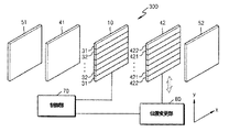
図1は、本発明の一実施形態による表示装置100を概略的に示す断面図である。
FIG. 1 is a cross-sectional view schematically showing a
図1を参照すれば、表示装置100は、外光の透過の可能な透明表示素子10上に第1偏光器51、第1リターダ41、パターンリターダ42及び第2偏光器52がさらに備えられる。
Referring to FIG. 1, the
透明表示素子10は、背面発光(bottom emission)する有機発光表示装置であり、第1基板1と、第1基板1上に備えられたディスプレイ部と、ディスプレイ部を密封する第2基板2とを備える。ディスプレイ部は、複数の画素に区切られているが、画素は、第1基板1の方向に光を放出する画素領域31、及び画素領域31に隣接して外光を透過する透過領域32を備える。
The
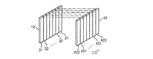
図2は、図1に示した透明表示素子10の概略的な平面図である。
FIG. 2 is a schematic plan view of the
図2に示したように、透明表示素子10のディスプレイ部には複数の画素が備えられ、複数の画素は、行方向及び列方向にマトリックス状に配列される。この時、透明表示素子10の画素領域31及び透過領域32が一方向に互いに繰り返されるパターンを持つように画素が配列される。これによって、透明表示素子10には、画素領域31及び透過領域32が一方向に一定間隔で規則的に形成される。
As shown in FIG. 2, the display unit of the
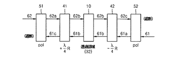
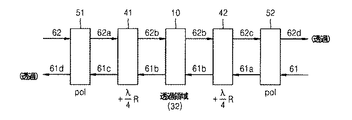
再び図1を参照すれば、透明表示素子10から順次に第1リターダ41及び第1偏光器51は、透明表示素子10が光を放出する第1基板1の外側に配される。第1偏光器51と第1リターダ41との組み合わせは、所定の方向に回転する円偏光(circularly polarized light)を通過させることを特徴とする。すなわち、第1偏光器51と第1リターダ41との組み合わせは、左円偏光または右円偏光のうち一種のみ通過させうるものであり、表示装置100の全面で外光の反射を低減させてユーザに画像を鮮やかに表示する。ここで第1偏光器51は、入射される光を所定の方向に線形偏光させる線形偏光器(linear polarizer)であり、第1リターダ41は、入射される光を+1/4波長(+λ/4)ほど位相遅延させる位相遅延器(retarder)である。第1リターダ41は、線形偏光を円偏光に変換するか、または円偏光を線形偏光に変換する。第1リターダ41は、接着物質によって透明表示素子10に貼り付けられ、またはフィルム状に透明表示素子10に貼り付けられる。
Referring to FIG. 1 again, the
透明表示素子10から順次にパターンリターダ42及び第2偏光器52は、透明表示素子10が光を放出しない側である第2基板2の外側に配される。ここで第2偏光器52は、入射される光を所定の方向に線形偏光させる線形偏光器である。パターンリターダ42は、入射される光を−1/4波長(−λ/4)だけ位相遅延させる第2リターダ421、及び入射される光を+1/4波長(+λ/4)だけ位相遅延させる第3リターダ422を持つ位相遅延器である。パターンリターダ42は、線形偏光を円偏光に変換するか、または円偏光を線形偏光に変換する。
In order from the
図3は、図1に示したパターンリターダの概略的な平面図である。 FIG. 3 is a schematic plan view of the pattern retarder shown in FIG.
図3に示したように、パターンリターダ42は、透明表示素子10の画素領域31及び透過領域32の繰り返しパターン方向と同方向に、第2リターダ421と第3リターダ422とを互いに繰り返して備える。これによって、本発明の実施形態は、第2リターダ421または第3リターダ422が透明表示素子10の周期的な透過領域32に対応するように、透明表示素子10に対してパターンリターダ42の相対的位置を調節することで、外光の透過率を制御する。
As shown in FIG. 3, the
パターンリターダ42の第2リターダ421の数及び第3リターダ422の数の和は、透明表示素子10の透過領域32に対応するラインの数の2倍より1だけ多い。この時、パターンリターダ42の位置制御方法によって、第2リターダ421の数が第3リターダ422の数より1だけ多いか、または第3リターダ422の数が第2リターダ421の数より1だけ多い。図2及び図3に示した透明表示素子10及びパターンリターダ42を参照すれば、例えば、透明表示素子10は、5ラインの透過領域32を備え、パターンリターダ42は、5個の第2リターダ421及び6個の第3リターダ422、すなわち、総数が11個のリターダを備える。図2及び図3に示した画素数及びリターダの数は、説明の便宜のために選択されたものであり、本発明はこれに限定されず、複数の画素及びリターダが備えられうるということはいうまでもない。
The sum of the number of the
パターンリターダ42は、例えば、配向膜と液晶膜とを含む構造に形成されることができる。配向膜は液晶膜の液晶分子を配向させ、公知の光配向性化合物を使える。液晶膜の液晶分子は配向膜の配向によって配向される。第2リターダ421または第2リターダ422が位置する領域ごとに配向膜の配向処理を異ならせることで液晶分子の配向状態を変換させ、位相遅延値が周期的に変わるパターンリターダ42を形成する。第2リターダ421及び第3リターダ422は、互いに延伸軸が垂直である。
The pattern retarder 42 can be formed, for example, in a structure including an alignment film and a liquid crystal film. The alignment film aligns the liquid crystal molecules of the liquid crystal film and can use a known photo-alignment compound. The liquid crystal molecules of the liquid crystal film are aligned by the alignment film. By changing the alignment process of the alignment film for each region where the
一方、本発明の一実施形態によれば、表示装置100は、第1偏光器51と第2偏光器52とが互いに同じ偏光軸を持つことができ、他の実施形態によれば、表示装置100は、第1偏光器51と第2偏光器52とが互いに異なる偏光軸を持つ。これらの2つの実施形態で、パターンリターダ42の位相遅延値の制御によって低電力で外光の透過率を変換できる表示装置100を具現することが、本発明の一側面による特徴である。
Meanwhile, according to an embodiment of the present invention, the
本発明の一実施形態によれば、第1偏光器51、第1リターダ41、パターンリターダ42及び第2偏光器52などの各種光学部材を備える表示装置100を開示し、これらの各種光学部材によって外光の透過度を調節できることを特徴とする。
According to an embodiment of the present invention, a
表示装置100の外光の透過度を調節するための一方法では、透明表示素子10の一側に液晶を配置させる。この場合、液晶を密封するために2枚のガラス基板が必要である。しかし、本発明の一実施形態によれば、パターンリターダ42及び各種光学部材特有の配置によって、液晶使用時に望まれるさらなるガラス基板が必要なく、低電力で表示装置の透過率を調節できるという効果がある。
In one method for adjusting the transmittance of external light of the
そして、液晶の波長分散性は、フィルム状の光学部材である第1リターダ41の波長分散性とは異なり、液晶の波長分散性と光学部材の波長分散性とを合わせ難いため、表示装置が全体的に波長分散性特性を持つようになる。ここで波長分散性とは、あらゆる波長の光に対して均一なブラック(Black)状態や透過(Transparent)状態にならない現象を意味する。しかし、本発明の一実施形態によれば、位相遅延値の異なるリターダが繰り返して配列された固体型のパターンリターダ42を使うため、光学部材である第1リターダ41とパターンリターダ42との波長分散性を合わせやすい。これによって、表示装置100が透過モードである時に外光の透過率を増加させ、ブラックモードである時に外光の透過率を減少させる。
Since the wavelength dispersion of the liquid crystal is different from the wavelength dispersion of the
また液晶を用いて外光の透過度を調節するためには、液晶密封工程と透明表示素子製造工程とが分離されないため工程が複雑である。そして、電気的方式で液晶の配列を調節することで外光の透過度を調節せねばならない。しかし、本発明の一実施形態によれば、透明表示素子10の製造工程と固体型のパターンリターダ42の製造工程とが完全に分離されることで工程が単純化する。そして、本発明の一実施形態によれば、パターンリターダ42を機械的/物理的移動方式によって位置変更することで、簡単に外光の透過度を調節できる。
Further, in order to adjust the transmittance of external light using liquid crystal, the liquid crystal sealing process and the transparent display element manufacturing process are not separated, and the process is complicated. Then, the transmittance of outside light must be adjusted by adjusting the alignment of the liquid crystal by an electrical method. However, according to an embodiment of the present invention, the manufacturing process of the
本発明の一実施形態によれば、表示装置100が光を透過する透過モード(transparent mode)である時、画像が具現される側に位置しているユーザが、第2基板2の外側から第1基板1の外側方向に透過する第1外光61を通じて第2基板2の外側のイメージを観察する。一方、画像が具現される反対側に位置しているユーザも、第1基板1の外側から第2基板2の外側に透過される第2外光62を通じて第1基板1の外側のイメージを観察する。ここで第1外光61は、画像と同方向に出る外光であり、第2外光62は、第1外光61と逆方向の外光である。
According to an exemplary embodiment of the present invention, when the
また、表示装置100が光を透過しないブラックモード(black mode)である時、画像が具現される側に位置しているユーザは、第2基板2の外側のイメージを観察できない。一方、画像が具現される反対側に位置しているユーザも、第1基板1の外側のイメージを観察できない。
In addition, when the
図4は、図1に示した透明表示素子10に含まれた画素の一実施形態を示すものである。そして、図5は、画素の他の実施形態を示すものである。
FIG. 4 shows an embodiment of a pixel included in the
画素は複数のサブ画素を含み、例えば、赤色サブ画素Pr、緑色サブ画素Pg、青色サブ画素Pbを含む。 The pixel includes a plurality of sub-pixels, for example, a red sub-pixel Pr, a green sub-pixel Pg, and a blue sub-pixel Pb.
各サブ画素Pr、Pg、Pbは、画素領域31及び透過領域32を備える。画素領域31には画素回路部311及び発光部312が備えられ、画素回路部311及び発光部312は、重畳しないように互いに隣接して配される。それによって初めて、発光部312が第1基板1の方向に背面発光する時、画素回路部311によって光路が邪魔されないからである。
Each subpixel Pr, Pg, Pb includes a
画素領域31に隣接して、外光を透過する透過領域32が配される。
Adjacent to the
透過領域32は、図4に示したように、各サブ画素Pr、Pg、Pb別に独立して備えられてもよく、図5に示したように、各サブ画素Pr、Pg、Pbにかけて互いに連結されるように備えられてもよい。すなわち、ディスプレイ部全体からみれば、画素は共通の透過領域32を介して互いに離隔している複数の画素領域31を備えられる。図5による実施形態の場合、外光が透過される透過領域32の面積が広くなる効果があるため、ディスプレイ部全体の透過率を高める。
As shown in FIG. 4, the
図5では、赤色サブ画素Pr、緑色サブ画素Pg及び青色サブ画素Pbの透過領域32がいずれも連結されたと示したが、本発明は必ずしもこれに限定されるのではなく、赤色サブ画素Pr、緑色サブ画素Pg及び青色サブ画素Pbのうち互いに隣接しているいずれか2つのサブ画素の透過領域32のみ互いに連結されるように備えられてもよい。
Although FIG. 5 shows that the
図6は、図4及び図5に示したサブ画素Pr、Pg、Pbのうちいずれか一つのサブ画素の断面を示すものである。 FIG. 6 shows a cross section of one of the sub-pixels Pr, Pg, and Pb shown in FIGS.
図6に示したように、画素領域31の画素回路部311には薄膜トランジスタTRが配されるが、図面に示したように必ずしも一つの薄膜トランジスタTRが配されることに限定されるものではなく、この薄膜トランジスタTRを備えるピクセル回路が備えられる。この画素回路には、薄膜トランジスタTR以外にも複数の薄膜トランジスタ及びストレージキャパシタがさらに備えられ、これらと連結されたスキャンライン、データライン及びVddラインなどの配線がさらに備えられる。
As shown in FIG. 6, the thin film transistor TR is disposed in the
画素領域の発光部312には、発光素子である有機発光素子ELが配される。この有機発光素子ELは、ピクセル回路の薄膜トランジスタTRと電気的に連結されている。
The
初めに、第1基板1上にはバッファ膜211が形成され、このバッファ膜211上に薄膜トランジスタTRを備えるピクセル回路が形成される。
First, a
次に、バッファ膜211上には半導体活性層212が形成される。
Next, the semiconductor
バッファ膜211は、不純元素の浸透を防止して表面を平坦化する役割を行うものであり、このような役割を行える多様な物質で形成される。一例として、バッファ膜211は、シリコンオキサイド、シリコンナイトライド、シリコンオキシナイトライド、アルミニウムオキサイド、アルミニウムナイトライド、チタンオキサイドまたはチタンナイトライドなどの無機物や、ポリイミド、ポリエステル、アクリルなどの有機物またはこれらの積層体で形成される。バッファ膜211は必須構成要素ではなく、必要に応じては備えられなくてもよい。
The
半導体活性層212は多結晶シリコンに形成されるが、必ずしもこれに限定されるものではなく、酸化物半導体で形成されうる。例えば、G−I−Z−O層[(In2O3)a(Ga2O3)b(ZnO)c層](a、b、cは、それぞれa≧0、b≧0、c>0の条件を満たす実数)でありうる。このように半導体活性層212を酸化物半導体で形成する場合には、画素領域31のうち画素回路部311での光透過度がさらに高くなり、これによってディスプレイ部全体の外光透過度を上昇させる。
The semiconductor
半導体活性層212を覆うようにゲート絶縁膜213がバッファ膜211上に形成され、ゲート絶縁膜213上にゲート電極214が形成される。
A
ゲート電極214を覆うように、ゲート絶縁膜213上に層間絶縁膜215が形成され、この層間絶縁膜215上にソース電極216及びドレイン電極217が形成され、それぞれ半導体活性層212及びコンタクトホールを通じてコンタクトされる。
An interlayer insulating
前述のような薄膜トランジスタTRの構造は、必ずしも図示されたところに限定されるものではなく、多様な形態の薄膜トランジスタの構造が適用できるということはいうまでもない。 The structure of the thin film transistor TR as described above is not necessarily limited to that illustrated, and it is needless to say that various types of thin film transistor structures can be applied.
このような薄膜トランジスタTRを覆うようにパッシベーション膜218が形成される。パッシベーション膜218は、上面の平坦化した単一または複数層の絶縁膜になる。このパッシベーション膜218は無機物及び/または有機物で形成される。パッシベーション膜218は、画素領域31及び透過領域32をいずれも覆うように形成される。しかし、これに限定されるものではなく、図示されていないが、パッシベーション膜218は透過領域32に対応する位置に開口部(図示せず)を備えることで透過領域32の外光透過効率をさらに高める。
A
パッシベーション膜218上には、薄膜トランジスタTRと電気的に連結された有機発光素子ELの第1電極221が形成される。第1電極221は、あらゆるサブピクセル別に独立したアイランド状に形成される。第1電極221は、画素領域31内の発光部312に位置し、画素回路部311と重畳しないように配される。
On the
パッシベーション膜218上には、有機及び/または無機絶縁物に備えられた画素定義膜219が形成される。
On the
画素定義膜219は、第1電極221のエッジを覆って中央部は露出させるように第3開口部219aを持つ。一方、この画素定義膜219は画素領域31を覆うように備えられるが、必ずしも画素領域31全体を覆うように備えられるものではなく、少なくとも一部、特に、第1電極221のエッジを覆うようにすればよい。この画素定義膜219は、透過領域32に対応する位置に第2開口部219bを備える。画素定義膜219が透過領域32には位置しないため、透過領域32の外光透過効率がさらに高くなる。
The
パッシベーション膜218及び画素定義膜219は、いずれも透明な物質からなる。絶縁膜が透明な物質からなることで、透明表示素子10の外光透過効率はさらに高くなる。
Both the
第3開口部219aを通じて露出された第1電極221上には、有機膜223及び第2電極222が順に積層される。第2電極222は、第1電極221と対向して、有機膜223及び画素定義膜219を覆って画素領域31内に位置する。第2電極222は、少なくとも画素領域31に形成され、透過領域32に対応する位置に第1開口部222aを備える。第2電極222が透過領域32には位置しないことで、透過領域32の外光透過効率がさらに高くなる。一方、第1開口部222aと第2開口部219bとは互いに連結される。
An
有機膜223は、低分子または高分子有機膜が使われる。低分子有機膜を使う場合、ホール注入層(HIL:Hole Injection Layer)、ホール輸送層(HTL:Hole Transport Layer)、発光層(EML:Emission Layer)、電子輸送層(ETL:Electron Transport Layer)、電子注入層(EIL:Electron Injection Layer)などが単一あるいは複合の構造で積層して形成され、使用可能な有機材料も銅フタロシアニン(CuPc:copper phthalocyanine)、N,N−ジ(ナフタレン−1−イル)−N,N’−ジフェニル−ベンジジン(NPB)、トリス(8−キノリノラト)アルミニウム(Alq3)などをはじめとして多様に適用できる。これら低分子有機膜は、真空蒸着法で形成される。この時、ホール注入層、ホール輸送層、電子輸送層、及び電子注入層などは共通層であり、赤色、緑色、青色のピクセルに共通に適用される。
The
第1電極221はアノード電極の機能を行い、第2電極222はカソード電極の機能を行えるが、もちろん、これら第1電極221及び第2電極222の極性は互いに逆になってもよい。
The
本発明の一実施形態によれば、第1電極221は透明電極になり、第2電極222は反射電極になる。第1電極221は、ITO、IZO、ZnO、またはIn2O3などの透明な導電性物質を含んで備えられる。そして第2電極222は、すなわち、Ag、Mg、Al、Pt、Pd、Au、Ni、Nd、Ir、Cr、Li、またはCaなどで形成される。よって、有機発光素子ELは、第1電極221の方向に画像を具現する背面発光型(bottom emission type)になる。この場合、第2電極222もディスプレイ部全体に電圧降下が起きないように十分な厚さで形成可能になって、大面積表示装置100に適用するのに十分である。
According to one embodiment of the present invention, the
図7は、本発明の他の実施形態による表示装置200を概略的に示す断面図である。
FIG. 7 is a cross-sectional view schematically illustrating a
図7に示した表示装置200は、図1に示した表示装置100と異なって、透明表示素子10が前面発光(top emission)する有機発光表示装置でありうる。よって、透明表示素子10から順次に第1リターダ41及び第1偏光器51は、透明表示素子10が光を放出する第2基板2の外側に配される。一方、透明表示素子10から順次にパターンリターダ42及び第2偏光器52は、透明表示素子10が光を放出しない側である第1基板1の外側に配される。その外の構成要素は、前述した図1ないし図3の実施形態の対応する構成要素とその機能が同一または類似しているので、これについての具体的な説明は略する。
Unlike the
本発明の一実施形態によれば、表示装置200が光を透過する透過モード(transparent mode)である時、画像が具現される側に位置しているユーザが、第1基板1の外側から第2基板2の外側に透過される第1外光61を通じて第1基板1の外側のイメージを観察する。一方、画像が具現される反対側に位置しているユーザも、第2基板2の外側から第1基板2の外側に透過される第2外光62を通じて第2基板2の外側のイメージを観察する。ここで第1外光61は、画像と同方向に出る外光であり、第2外光62は、第1外光61と逆方向の外光である。
According to an exemplary embodiment of the present invention, when the
また、表示装置200が光を透過しないブラックモードである時、画像が具現される側に位置しているユーザは、第1基板1の外側のイメージを観察できない。一方、画像が具現される反対側に位置しているユーザも、第2基板2の外側のイメージを観察できない。
In addition, when the
図8は、図7に示した透明表示素子10に含まれた画素の一実施形態を示すものである。そして、図9は、画素の他の実施形態を示すものである。
FIG. 8 shows an embodiment of a pixel included in the
図8及び図9に示した画素は、図4及び図5に示した画素とは異なって、画素領域31に備えられる画素回路部311及び発光部312が互いに重畳するように配される。発光部312が第2基板2の方向に前面発光するので、画素回路部311と発光部312とが互いに重畳してもよい。これに加えて、発光部312がピクセル回路を備える画素回路部311を遮蔽することで、ピクセル回路による光干渉を排除できる特徴がある。その他の構成要素は、前述した図4及び図5の実施形態の対応する構成要素とその機能が同一または類似しているので、これについての具体的な説明は略する。
Unlike the pixels shown in FIGS. 4 and 5, the pixels shown in FIGS. 8 and 9 are arranged such that a
透過領域32は、図8に示したように、各サブ画素Pr、Pg、Pb別に独立して備えられてもよく、図9に示したように、各サブ画素Pr、Pg、Pbにかけて互いに連結されるように備えられてもよい。
As shown in FIG. 8, the
図10は、図8及び図9に示したサブ画素Pr、Pg、Pbのうちいずれか一つのサブ画素の断面を示すものである。 FIG. 10 shows a cross section of one of the sub-pixels Pr, Pg, and Pb shown in FIGS.
図10に示したように、画素回路部311には薄膜トランジスタTRが配され、発光部312には発光素子である有機発光素子ELが配される。
As shown in FIG. 10, the
第1基板1上にバッファ膜211が形成され、バッファ膜211上に半導体活性層212が形成され、半導体活性層212上にゲート絶縁膜213、ゲート電極214、層間絶縁膜215が形成される。層間絶縁膜215上にはソースドレイン電極216、217が形成される。このような薄膜トランジスタTRを覆うように、絶縁膜の一種であるパッシベーション膜218が形成される。パッシベーション膜218は、画素領域31及び透過領域32をいずれも覆うように形成される。しかし、これに限定されるものではなく、図示されていないが、パッシベーション膜218は、透過領域32に対応する位置に開口部(図示せず)を備えることで透過領域の外光透過効率をさらに高める。
A
パッシベーション膜218上には、薄膜トランジスタTRと電気的に連結された有機発光素子ELの第1電極221が形成される。第1電極221は画素領域31内の発光部312に位置し、画素回路部311と重畳して画素回路部311を遮蔽するように配される。
On the
パッシベーション膜218上には、有機及び/または無機絶縁物からなる画素定義膜219が形成される。
A
画素定義膜219は、第1電極221のエッジを覆って中央部は露出させるように第3開口部219aを持つ。一方、この画素定義膜219は、画素領域31を覆うように備えられるが、必ずしも画素領域31全体を覆うように備えられるものではなく、少なくとも一部、特に、第1電極221の端を覆うようにすればよい。この画素定義膜219は、透過領域32に対応する位置に第2開口部219bを備える。画素定義膜219が透過領域32には位置しないため、透過領域32の外光透過効率がさらに高くなる。
The
パッシベーション膜218及び画素定義膜219はいずれも透明な物質からなる。絶縁膜が透明な物質からなることで、透明表示素子10の外光透過効率はさらに高くなる。
Both the
第3開口部219aを通じて露出された第1電極221上には、有機膜223及び第2電極222が順に積層される。第2電極222は少なくとも画素領域31に形成され、透過領域32に対応する位置に第1開口部222aを備える。第2電極222が透過領域32には位置しないため、透過領域32の外光透過効率がさらに高くなる。一方、第1開口部222aと第2開口部219bとは互いに連結される。
An
図10に示した本発明の一実施形態によれば、ここで第1電極221は、透明な導電体及び反射膜の積層構造で形成され、第2電極222は、半反射半透過電極になる。ここで透明な導電体は、仕事関数の高いITO、IZO、ZnO、またはIn2O3などからなる。一方、反射膜は、Ag、Mg、Al、Pt、Pd、Au、Ni、Nd、Ir、Cr、Li、Ca、Mo及びこれらの合金からなる群から選択された少なくとも一つの金属を含むことを特徴とする。ここで第1電極221は、画素領域31内に形成される。
According to the embodiment of the present invention shown in FIG. 10, the
第2電極222は、Ag、Mg、Al、Pt、Pd、Au、Ni、Nd、Ir、Cr、Li、Ca、Moまたはこれらの合金などで形成される。ここで第2電極222は、透過率が高いように100ないし300Åの厚さの薄膜で形成することが望ましい。よって、有機発光素子ELは、第2電極222の方向に画像を具現する前面発光型になる。
The
図11は、本発明の一実施形態による表示装置の動作を概略的に説明するための図面である。 FIG. 11 is a view for schematically explaining the operation of the display device according to the embodiment of the present invention.
図11を参照すれば、表示装置300は、タブレットコンピュータ、メディア保存装置、携帯電話、個人携帯端末などの映像を処理及び表示する電子装置である。表示装置300は、第1偏光器51、第1リターダ41、透明表示素子10、パターンリターダ42及び第2偏光器52を備える。図11に示した表示装置300は、図1及び図7に示した表示装置100、200である。そして、表示装置300は、制御部70及び位置変更部80を備える。以下では、図1及び図7の実施形態と対応する構成要素についての具体的な説明は略する。
Referring to FIG. 11, the
透明表示素子10は、画素領域31と透過領域32とが列方向(y軸)に繰り返して配列されたパターンを持つ。パターンリターダ42は、第2リターダ421及び第3リターダ422が、透明表示素子10の画素領域31及び透過領域32に対応して列方向に繰り返して配列されたパターンを持つ。
The
制御部70は、透明表示素子10の駆動のためのドライバIC(図示せず)を備える。ドライバICは、透明表示素子10のディスプレイ部に形成された複数のスキャンラインSにスキャン信号を印加するスキャンドライバ、及び複数のデータラインDにデータ信号を印加するデータドライバを備える。そして、制御部70は、外光の透過率制御のための制御信号を位置変更部80に出力する。
The
位置変更部80は制御信号によって、パターンリターダ42を所定距離ほど機械的/物理的に移動させ、透明表示素子10との相対的な位置を変化させる。例えば、位置変更部80は、パターンリターダ42を垂直方向(y軸)に上下移動させることで、透明表示素子10を透過する外光の透過率を制御する。パターンリターダ42の位置変化量(移動距離)は、画素ピッチの略半分(1/2)に対応する。例えば、パターンリターダ42の位置変化量は約200μmである。
The
図12Aないし図12Cは、図11に示した透明表示素子とパターンリターダとの相対的な位置変化を説明する例示図である。図12Aないし図12Cの点線は、透明表示素子10とパターンリターダ42との位置対応関係を説明するために示した。
12A to 12C are exemplary diagrams for explaining a relative position change between the transparent display element and the pattern retarder shown in FIG. The dotted lines in FIGS. 12A to 12C are shown for explaining the positional correspondence between the
図12Aに示したように、初期に、パターンリターダ42は、入射光を+λ/4ほど位相遅延させる第3リターダ422が透明表示素子10の画素領域31に対応し、入射光を−λ/4ほど位相遅延させる第2リターダ421が、透明表示素子10の透過領域32に対応するように配される。
As shown in FIG. 12A, in the initial stage, the
表示装置300は位置変更部80を用いて、パターンリターダ42を垂直方向(y軸)に上下移動を制御することで、透明表示素子10とパターンリターダ42との相対的位置を変更させて外光の透過率を制御する。
The
図12Bに示したように、パターンリターダ42は下方に所定距離移動するか、または、図12Cに示したように、パターンリターダ42は上方に所定距離移動し、パターンリターダ42の入射光を−λ/4ほど位相遅延させる第2リターダ421が透明表示素子10の画素領域31に対応し、入射光を+λ/4ほど位相遅延させる第3リターダ422が透明表示素子10の透過領域32に対応するように配される。
As shown in FIG. 12B, the
しかし、本発明の実施形態はこれに限定されず、初期にパターンリターダ42は、入射光を−λ/4ほど位相遅延させる第2リターダ421が透明表示素子10の画素領域31に対応し、入射光を+λ/4ほど位相遅延させる第3リターダ422が透明表示素子10の透過領域32に対応するように配される。そして、パターンリターダ42を上方または下方に所定距離移動させて、パターンリターダ42は、入射光を+λ/4ほど位相遅延させる第3リターダ422が透明表示素子10の画素領域31に対応し、入射光を−λ/4ほど位相遅延させる第2リターダ421が透明表示素子10の透過領域32に対応するように配される。
However, the embodiment of the present invention is not limited to this. In the initial stage, the
図13は、本発明の他の実施形態による表示装置の動作を概略的に説明するための図面である。 FIG. 13 is a view for schematically explaining an operation of a display device according to another exemplary embodiment of the present invention.
図13に示した表示装置400は、図11に示した表示装置300とは異なって、透明表示素子10は、画素領域31及び透過領域32が行方向(x軸)に繰り返して配列されたパターンを持ち、パターンリターダ42は、第2リターダ421及び第3リターダ422が透明表示素子10の画素領域31及び透過領域32に対応して行方向に繰り返して配列されたパターンを持つ。よって、位置変更部80は、制御部70が出力する制御信号によって、パターンリターダ42を水平方向(x軸)に左右移動させることで、透明表示素子10を透過する外光の透過率を制御する。パターンリターダ42の位置変化量(移動距離)は、画素ピッチの略半分(1/2)に対応する。
The
その外の構成要素は、前述した図11の実施形態の対応する構成要素とその機能が同一または類似しているので、これについての具体的な説明は略する。 The other components have the same or similar functions as the corresponding components in the embodiment of FIG. 11 described above, and a specific description thereof will be omitted.
図14Aないし図14Cは、図13に示した透明表示素子とパターンリターダとの相対的な位置変化を説明する例示図である。図14Aないし図14Cの点線は、透明表示素子10とパターンリターダ42との位置対応関係を説明するために示した。
14A to 14C are exemplary diagrams for explaining a relative position change between the transparent display element and the pattern retarder shown in FIG. The dotted lines in FIGS. 14A to 14C are shown for explaining the positional correspondence between the
図14Aに示したように、初期に、パターンリターダ42は、入射光を+λ/4ほど位相遅延させる第3リターダ422が透明表示素子10の画素領域31に対応し、入射光を−λ/4ほど位相遅延させる第2リターダ421が透明表示素子10の透過領域32に対応するように配される。
As shown in FIG. 14A, initially, the
表示装置300は位置変更部80を用いて、図14Bに示したように、パターンリターダ42を左方に所定距離移動させるか、または、図14Cに示したように、パターンリターダ42を右方に所定距離移動させて、パターンリターダ42の入射光を−λ/4ほど位相遅延させる第2リターダ421が透明表示素子10の画素領域31に対応し、入射光を+λ/4ほど位相遅延させる第3リターダ422が透明表示素子10の透過領域32に対応するように配される。
The
しかし、本発明の実施形態はこれに限定されず、初期にパターンリターダ42は、入射光を−λ/4ほど位相遅延させる第2リターダ421が透明表示素子10の画素領域31に対応し、入射光を+λ/4ほど位相遅延させる第3リターダ422が透明表示素子10の透過領域32に対応するように配される。そして、パターンリターダ42を左方または右方に所定距離移動させ、パターンリターダ42は、入射光を+λ/4ほど位相遅延させる第3リターダ422が透明表示素子10の画素領域31に対応し、入射光を−λ/4ほど位相遅延させる第2リターダ421が透明表示素子10の透過領域32に対応するように配される。
However, the embodiment of the present invention is not limited to this. In the initial stage, the
図15及び図16は、本発明の一実施形態による偏光板とリターダとの組み合わせによる表示装置の外光透過率調節を説明する図面である。図15及び図16で、画像の方向と逆方向に進む光、すなわち、前面入射光である第2外光62と、画像の方向と同方向に進む光、すなわち、背面入射光である第1外光61と、を用いて説明する。
FIG. 15 and FIG. 16 are diagrams for explaining external light transmittance adjustment of a display device by a combination of a polarizing plate and a retarder according to an embodiment of the present invention. 15 and 16, the light traveling in the direction opposite to the image direction, that is, the second
図15は、図12Aまたは図14Aに示した透明表示素子とパターンリターダとの相対的な位置関係による表示装置の外光透過率調節を説明する図面である。 FIG. 15 is a diagram for explaining external light transmittance adjustment of the display device according to the relative positional relationship between the transparent display element and the pattern retarder shown in FIG. 12A or 14A.
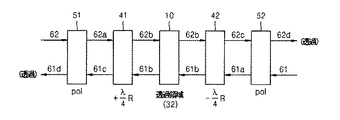
図15を参照すれば、入射光を−1/4波長(−λ/4)ほど遅延させるパターンリターダ42の第2リターダ421が透明表示素子10の透過領域32に対応するように、透明表示素子10とパターンリターダ42との相対的な位置が制御される。第1リターダ41は、前述したように入射光を+1/4波長(+λ/4)ほど遅延させる位相遅延器である。よって、第1リターダ41とパターンリターダ42の第2リターダ421とは、その入射光を、絶対値のサイズは同じものの方向が相異なるように位相遅延させる。これに加えて、第1偏光器51及び第2偏光器52は互いに同じ方向の偏光軸を持つ。
Referring to FIG. 15, the transparent display element is configured such that the
第2外光62は、第1偏光器51を経つつ線形偏光された第2a外光62aになる。第2a外光62aは、第1リターダ41を経つつ位相が+1/4波長(+λ/4)ほど遅延した第2b外光62bになる。第2b外光62bは、透明表示素子10の透過領域32を通過し、パターンリターダ42の第2リターダ421を経つつ位相が再び−1/4波長(−λ/4)ほど遅延した第2c外光62cになる。第2c外光62cは、第2偏光器52を経つつ線形偏光された第2d外光62dになる。
The second
第1外光61は、第2偏光器52を経つつ線形偏光された第1a外光61aになる。第1a外光61aは、パターンリターダ42の第2リターダ421を経つつ位相が−1/4波長(−λ/4)ほど遅延した第1b外光61bになる。第1b外光61bは透明表示素子10の透過領域32を通過し、第1リターダ41を経つつ位相が再び+1/4波長(+λ/4)ほど遅延した第1c外光61cになる。第1c外光61cは、第1偏光器51を経つつ線形偏光された第1d外光61dになる。
The first
結果的に、図15のように、第1偏光器51及び第2偏光器52が同方向の偏光軸を持ち、パターンリターダ42の透過領域32に対応するリターダが第1リターダ41と互いに異なる位相遅延値を持つようにパターンリターダ42の位置が制御される場合、第1外光61及び第2外光62は透過される。すなわち、パターンリターダ42の位置制御によって透過される外光の位相遅延値を定めることで、表示装置の透過モードを容易に具現する。
As a result, as shown in FIG. 15, the
一方、ユーザは、透明表示素子10の画素領域31から放出される光によって、画像を見られる。
On the other hand, the user can see the image by the light emitted from the
図16は、図12B、図12C、図14Bまたは図14Cに示した透明表示素子とパターンリターダとの相対的な位置関係による表示装置の外光透過率調節を説明する図面である。 FIG. 16 is a view for explaining adjustment of the external light transmittance of the display device according to the relative positional relationship between the transparent display element shown in FIG. 12B, FIG. 12C, FIG. 14B or FIG. 14C and the pattern retarder.
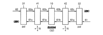
図16を参照すれば、入射光を+1/4波長(+λ/4)ほど遅延させるパターンリターダ42の第3リターダ422が透明表示素子10の透過領域32に対応するように、透明表示素子10とパターンリターダ42との相対的な位置が制御される。第1リターダ41は、前述したように入射光を+1/4波長(+λ/4)ほど遅延させる位相遅延器である。よって、第1リターダ41とパターンリターダ42の第3リターダ422とは、入射光を同じサイズ及び同方向に位相遅延させる。これに加えて、第1偏光器51と第2偏光器52とは互いに同じ方向の偏光軸を持つ。
Referring to FIG. 16, the
第2外光62は、第1偏光器51を経つつ線形偏光された第2a外光62aになる。第2a外光62aは、第1リターダ41を経つつ位相が+1/4波長(+λ/4)ほど遅延した第2b外光62bになる。第2b外光62bは透明表示素子10の透過領域32を通過し、パターンリターダ42の第3リターダ422を経つつ位相が再び+1/4波長(+λ/4)ほど遅延した第2c外光62cになる。第2c外光62cは、第2偏光器52を経つつ第1偏光器51と同方向に線形偏光され、第2c外光62cは遮断される。
The second
第1外光61は、第2偏光器52を経つつ線形偏光された第1a外光61aになる。第1a外光61aは、パターンリターダ42の第3リターダ422を経つつ位相が+1/4波長(−λ/4)ほど遅延した第1b外光61bになる。第1b外光61bは透明表示素子10の透過領域32を通過し、第1リターダ41を経つつ位相が再び+1/4波長(+λ/4)ほど遅延した第1c外光61cになる。第1c外光61cは、第1偏光器51を経つつ第2偏光器52と同方向に線形偏光され、第1c外光61cは遮断される。
The first
結果的に、図16のように、第1偏光器51及び第2偏光器52が同方向の偏光軸を持ち、パターンリターダ42の透過領域32に対応するリターダが第1リターダ41と互いに同じ位相遅延値を持つように位置制御される場合、第1外光61及び第2外光62は遮断される。すなわち、パターンリターダ42の位置制御によって透過される外光の位相遅延値を定めることで、表示装置300のブラックモードを容易に具現する。
As a result, as shown in FIG. 16, the
一方、ユーザは、透明表示素子10の画素領域31から放出される光によって画像を見ることができる。
On the other hand, the user can view an image by light emitted from the
本発明の実施形態は、図15及び図16のように、第1偏光器51及び第2偏光器52が同方向の偏光軸を持ち、パターンリターダ42の物理的移動によって透明表示素子10とパターンリターダ42との相対的位置を制御することで、表示装置300の透過モードとブラックモードとのスイチングを容易に具現する。
In the embodiment of the present invention, as shown in FIGS. 15 and 16, the
図17及び図18は、本発明の他の実施形態による偏光板とリターダとの組み合わせによる表示装置の外光透過率調節を説明する図面である。図17及び図18で、画像の方向と逆方向に進む光、すなわち、前面入射光である第2外光62と、画像の方向と同方向に進む光、すなわち、背面入射光である第1外光61とを用いて説明する。
FIG. 17 and FIG. 18 are diagrams for explaining external light transmittance adjustment of a display device by a combination of a polarizing plate and a retarder according to another embodiment of the present invention. 17 and 18, the light traveling in the opposite direction to the image direction, that is, the second
図17は、図12Aまたは図14Aに示した透明表示素子とパターンリターダとの相対的な位置関係による表示装置の外光透過率調節を説明する図面である。 FIG. 17 is a diagram for explaining external light transmittance adjustment of the display device according to the relative positional relationship between the transparent display element and the pattern retarder shown in FIG. 12A or 14A.
図17を参照すれば、入射光を−1/4波長(−λ/4)ほど遅延させるパターンリターダ42の第2リターダ421が透明表示素子10の透過領域32に対応するように、透明表示素子10とパターンリターダ42との相対的な位置が制御される。第1リターダ41は、前述したように入射光を+1/4波長(+λ/4)ほど遅延させる位相遅延器である。よって、第1リターダ41とパターンリターダ42の第2リターダ421とは、入射光を絶対値のサイズは同じものの方向が相異なるように位相遅延させる。これに加えて、第1偏光器51と第2偏光器52とは、互いに直交する方向の偏光軸を持つ。
Referring to FIG. 17, the transparent display element is configured such that the
第2外光62は、第1偏光器51を経つつ線形偏光された第2a外光62aになる。第2a外光62aは、第1リターダ41を経つつ位相が+1/4波長(+λ/4)ほど遅延した第2b外光62bになる。第2b外光62bは透明表示素子10の透過領域32を通過し、パターンリターダ42の第2リターダ421を経つつ位相が再び−1/4波長(−λ/4)ほど遅延した第2c外光62cになる。第2c外光62cは、第2偏光器52を経つつ第1偏光器51と異なる方向に線形偏光され、第2c外光62cは遮断される。
The second
第1外光61は、第2偏光器52を経つつ線形偏光された第1a外光61aになる。第1a外光61aは、第2リターダ421を経つつ位相が−1/4波長(−λ/4)ほど遅延した第1b外光61bになる。第1b外光61bは、透明表示素子10の透過領域32を通過し、第1リターダ41を経つつ位相が再び+1/4波長(+λ/4)ほど遅延した第1c外光61cになる。第1c外光61cは、第1偏光器51を経つつ第2偏光器52と異なる方向に線形偏光され、第1c外光61cは遮断される。
The first
結果的に、図16のように、第1偏光器51及び第2偏光器52が互いに垂直である偏光軸を持ち、パターンリターダ42の透過領域32に対応するリターダが第1リターダ41と互いに異なる位相遅延値を持つようにパターンリターダ42の位置が制御される場合、第1外光61及び第2外光62は遮断される。すなわち、パターンリターダ42の位置制御によって透過される外光の位相遅延値を定めることで、表示装置300のブラックモードを容易に具現する。
As a result, as shown in FIG. 16, the
一方、ユーザは、透明表示素子10の画素領域31から放出される光によって画像を見られる。
On the other hand, the user can see the image by the light emitted from the
図18は、図12B、図12C、図14Bまたは図14Cに示した透明表示素子とパターンリターダとの相対的な位置関係による表示装置の外光透過率調節を説明する図面である。 FIG. 18 is a diagram for explaining external light transmittance adjustment of the display device according to the relative positional relationship between the transparent display element shown in FIG. 12B, FIG. 12C, FIG. 14B, or FIG. 14C and the pattern retarder.
図18を参照すれば、入射光を+1/4波長(+λ/4)ほど遅延させるパターンリターダ42の第3リターダ422が透明表示素子10の透過領域32に対応するように、透明表示素子10とパターンリターダ42との相対的な位置が制御される。第1リターダ41は、前述したように入射光を+1/4波長(+λ/4)ほど遅延させる位相遅延板である。よって、第1リターダ41とパターンリターダ42の第3リターダ422とは、同じサイズ及び同方向に位相遅延させる。これに加えて、第1偏光器51と第2偏光器52とは、互いに直交する方向の偏光軸を持つ。
Referring to FIG. 18, the
第2外光62は、第1偏光器51を経つつ線形偏光された第2a外光62aになる。第2a外光62aは、第1リターダ41を経つつ位相が+1/4波長(+λ/4)ほど遅延した第2b外光62bになる。第2b外光62bは透明表示素子10の透過領域32を通過し、パターンリターダ42の第3リターダ422を経つつ位相が再び+1/4波長(+λ/4)ほど遅延した第2c外光62cになる。第2c外光62cは、第2偏光器52を経つつ第1偏光器51と異なる方向に線形偏光され、第2d外光62dになる。
The second
第1外光61は、第2偏光器52を経つつ線形偏光された第1a外光61aになる。第1a外光61aは、パターンリターダ42の第3リターダ422を経つつ位相が+1/4波長(+λ/4)ほど遅延した第1b外光61bになる。第1b外光61bは透明表示素子10の透過領域32を通過し、第1リターダ41を経つつ位相が再び+1/4波長(+λ/4)ほど遅延した第1c外光61cになる。第1c外光61cは、第1偏光器51を経つつ第2偏光器52と異なる方向に線形偏光され、第1d外光61dになる。
The first
結果的に、図18のように、第1偏光器51及び第2偏光器52が互いに垂直である偏光軸を持ち、パターンリターダ42の透過領域32に対応するリターダが第1リターダ41と同じ位相遅延値を持つように位置制御される場合、第1外光61及び第2外光62は透過される。すなわち、パターンリターダ42の位置制御によって位相遅延値を定めることで、表示装置300の透過モードを容易に具現する。
As a result, as shown in FIG. 18, the
一方、ユーザは、透明表示素子10の画素領域31から放出される光によって画像を見られる。
On the other hand, the user can see the image by the light emitted from the
本発明の実施形態は、図17及び図18のように、第1偏光器51及び第2偏光器52が互いに垂直方向の偏光軸を持ち、パターンリターダ42の物理的移動によって透明表示素子10とパターンリターダ42との相対的位置を制御することで、表示装置300のブラックモード及び透過モードのスイチングを容易に具現する。
In the embodiment of the present invention, as shown in FIGS. 17 and 18, the
図19は、本発明の他の実施形態による表示装置500を概略的に示す断面図である。
FIG. 19 is a cross-sectional view schematically illustrating a
図19の表示装置500は、透明表示装置10が放出する光路上に第1円偏光器71を配し、透明表示装置10が放出する光路の反対側に第2円偏光器72を配する。第1円偏光器71は、前述した表示装置100ないし400の第1リターダ41及び第1偏光器51の組み合わせを入れ替え、第2円偏光器72は、パターンリターダ42及び第2偏光器52の組み合わせを入れ替える。その外の構成要素は、前述した表示装置100ないし400の対応する構成要素とその機能及び動作が同一または類似しているので、これについての具体的な説明は略する。
In the
第1円偏光器71は、入射される光を+1/4波長(+λ/4)ほど位相遅延させつつ円形偏光させる。第2円偏光器72は、第1円偏光器72と同一または垂直方向の偏光軸を持ち、入射される光を−1/4波長(−λ/4)ほど位相遅延させる第1遅延領域と、入射される光を+1/4波長(+λ/4)ほど位相遅延させる第2遅延領域とが繰り返して形成されたパターンを持つ。第1遅延領域と第2遅延領域とは、互いに延伸軸が垂直である。
The first
したがって、表示装置500は、第2円偏光器72のパターン方向に沿って第1遅延領域または第2遅延領域が透明表示素子の透過領域32に対応するように、位置変更部80によって第2円偏光器72を上下または左右に一定距離移動させることで、表示装置500の外光を透過または遮断する。
Therefore, in the
図19の実施形態による表示装置500は、前述した実施形態による表示装置100ないし400がリターダ及び線偏光器を配する2回の工程を、円偏光器を配する1回の工程に低減して表示装置500を製造する。また、リターダのAR(Anti−Reflect)特性を別途に合わせる必要なく、円偏光器でAR特性を合わせることで工程が簡素化する。
The
本発明は、添付した図面に示した一実施形態を参照として説明されたが、これは例示的なものに過ぎず、当業者ならば、これから多様な変形及び均等な他の実施形態が可能であるという点を理解できるであろう。したがって、本発明の真の保護範囲は添付した特許請求の範囲のみによって定められなければならない。 Although the present invention has been described with reference to one embodiment shown in the accompanying drawings, this is merely illustrative, and various modifications and equivalent other embodiments may be made by those skilled in the art. You will understand that there is. Accordingly, the true protection scope of the present invention should be determined solely by the appended claims.
本発明は、表示装置関連の技術分野に好適に用いられる。 The present invention is suitably used in the technical field related to display devices.
100、200、300、400 表示装置
10 透明表示素子
31 画素領域(第1領域)
32 透過領域(第2領域)
41 第1リターダ
42 パターンリターダ
421 第2リターダ
422 第3リターダ
51 第1偏光器
52 第2偏光器
61 第1外光
62 第2外光
70 制御部
80 位置変更部
100, 200, 300, 400
32 Transmission area (second area)
41
Claims (30)
前記透明表示素子が放出する光路上に配されて前記外光を線形偏光させる第1偏光器と、
前記第1偏光器と前記透明表示素子との間に配されて前記外光の位相を遅延させる第1リターダと、
前記透明表示素子が放出する光路の反対側に配されて前記外光を線形偏光させる第2偏光器と、
前記第2偏光器と前記透明表示素子との間に配され、前記透明表示素子の前記第1領域と前記第2領域との配列方向と同方向に前記外光の波長を第1位相だけ遅延させる第2リターダと、第2位相だけ遅延させる第3リターダとが交互に配列されたパターンリターダと、を備える、光透過率制御の可能な表示装置。 Transparent display elements in which first regions that emit light and second regions that transmit external light adjacent to the first regions are alternately arranged in one direction;
A first polarizer disposed on an optical path from which the transparent display element emits to linearly polarize the external light;
A first retarder disposed between the first polarizer and the transparent display element to delay the phase of the external light;
A second polarizer disposed on the opposite side of the optical path from which the transparent display element emits to linearly polarize the external light;
A wavelength of the external light is delayed by a first phase in the same direction as the arrangement direction of the first area and the second area of the transparent display element, which is disposed between the second polarizer and the transparent display element. A display device capable of controlling light transmittance, comprising: a second retarder to be operated; and a pattern retarder in which third retarders to be delayed by the second phase are alternately arranged.
前記第3リターダが前記第2領域に対応するように前記パターンリターダの位置が調節されれば、前記表示装置が、前記外光を透過させることを特徴とする、請求項3に記載の光透過率制御の可能な表示装置。 The absolute values of the first phase and the second phase are the same, the rotation direction is different,
The light transmission according to claim 3, wherein the display device transmits the external light when the position of the pattern retarder is adjusted so that the third retarder corresponds to the second region. Display device capable of rate control.
前記第2リターダが前記第2領域に対応するように前記パターンリターダの位置が調節されれば、前記表示装置が、前記外光を遮断することを特徴とする、請求項3に記載の光透過率制御の可能な表示装置。 The absolute values of the first phase and the second phase are the same, the rotation direction is different,
The light transmission according to claim 3, wherein the display device blocks the external light when the position of the pattern retarder is adjusted so that the second retarder corresponds to the second region. Display device capable of rate control.
前記第3リターダが前記第2領域に対応するように前記パターンリターダの位置が調節されれば、前記表示装置が、前記外光を遮断することを特徴とする請求項6に記載の光透過率制御の可能な表示装置。 The absolute values of the first phase and the second phase are the same, the rotation direction is different,
The light transmittance according to claim 6, wherein the display device blocks the external light when the position of the pattern retarder is adjusted so that the third retarder corresponds to the second region. Controllable display device.
前記第2リターダが前記第2領域に対応するように前記パターンリターダの位置が調節されれば、前記表示装置が、前記外光を透過することを特徴とする、請求項6に記載の光透過率制御の可能な表示装置。 The absolute values of the first phase and the second phase are the same, the rotation direction is different,
The light transmission according to claim 6, wherein if the position of the pattern retarder is adjusted so that the second retarder corresponds to the second region, the display device transmits the external light. Display device capable of rate control.
前記パターンリターダの前記第2リターダと前記第3リターダとが、前記透明表示素子に対応して垂直方向に交互に配列されることを特徴とする、請求項1に記載の光透過率制御の可能な表示装置。 The first region and the second region of the transparent display element are alternately arranged in a vertical direction,
2. The light transmittance control according to claim 1, wherein the second retarder and the third retarder of the pattern retarder are alternately arranged in a vertical direction corresponding to the transparent display element. Display device.
前記パターンリターダの前記第2リターダと前記第3リターダとが、前記透明表示素子に対応して水平方向に交互に配列されることを特徴とする、請求項1に記載の光透過率制御の可能な表示装置。 The first region and the second region of the transparent display element are alternately arranged in a horizontal direction,
2. The light transmittance control according to claim 1, wherein the second retarder and the third retarder of the pattern retarder are alternately arranged in a horizontal direction corresponding to the transparent display element. Display device.
前記透明表示素子が放出する光路上に配され、前記外光の波長を第1位相だけ遅延させて円形偏光させる第1円偏光器と、
前記透明表示素子が放出する光路の反対側に配され、前記外光を前記第1位相だけ遅延させる第1遅延領域と、第2位相だけ遅延させる第2遅延領域とが、前記透明表示素子の前記第1領域及び前記第2領域との配列方向と同方向に繰り返し形成され、前記外光を前記第1位相または前記第2位相だけ遅延させつつ円偏光させる第2円偏光器と、を備える、光透過率制御の可能な表示装置。 Transparent display elements in which first regions that emit light and second regions that transmit external light adjacent to the first regions are alternately arranged in one direction;
A first circular polarizer disposed on an optical path from which the transparent display element emits, and circularly polarizes the external light by delaying the wavelength of the external light by a first phase;
A first delay region that is arranged on the opposite side of the optical path from which the transparent display element emits and delays the external light by the first phase, and a second delay region that delays the second phase by the second phase, A second circular polarizer that is repeatedly formed in the same direction as the arrangement direction of the first region and the second region, and circularly polarizes the external light while being delayed by the first phase or the second phase. Display device capable of controlling light transmittance.
前記透明表示素子が放出する光路上に配されて前記外光を線形偏光させる第1偏光器と、第1偏光器と前記透明表示素子との間に配されて前記外光の波長を前記第1位相だけ遅延させる第1リターダと、を備え、
前記第2円偏光器が、
前記透明表示素子が放出する光路の反対側に配されて前記外光を線形偏光させる第2偏光器と、前記第2偏光器と前記透明表示素子との間に配され、前記外光の波長を前記第1位相だけ遅延させる第2リターダと、前記第2位相だけ遅延させる第3リターダとが交互に配列されたパターンリターダと、を備える、請求項16に記載の光透過率制御の可能な表示装置。 The first circular polarizer is
A first polarizer disposed on an optical path from which the transparent display element emits to linearly polarize the external light; and a first polarizer that is disposed between the first polarizer and the transparent display element to change the wavelength of the external light. A first retarder that delays by one phase;
The second circular polarizer is
A second polarizer for linearly polarizing the external light disposed on the opposite side of the light path emitted by the transparent display element; and a wavelength of the external light disposed between the second polarizer and the transparent display element. A light retarder capable of controlling light transmittance according to claim 16, comprising: a second retarder that delays the second retarder by the first phase; and a pattern retarder in which third retarders that are delayed by the second phase are alternately arranged. Display device.
前記第1円偏光器及び前記第2円偏光器が、互いに同じ方向の偏光軸を持ち、
前記第2円偏光器の前記第1遅延領域または前記第2遅延領域が前記第2領域に対応するように、前記第2円偏光器と前記透明表示素子との相対的位置を調節して前記外光を遮断または透過させる位置変更部をさらに備える、請求項16に記載の光透過率制御の可能な表示装置。 The absolute values of the first phase and the second phase are the same, the rotation direction is different,
The first circular polarizer and the second circular polarizer have polarization axes in the same direction,
The relative position between the second circular polarizer and the transparent display element is adjusted so that the first delay region or the second delay region of the second circular polarizer corresponds to the second region. The display device capable of controlling light transmittance according to claim 16, further comprising a position changing unit that blocks or transmits external light.
前記第1円偏光器と前記第2円偏光器とが、互いに直交する方向の偏光軸を持ち、
前記第2円偏光器の前記第1遅延領域または前記第2遅延領域が前記第2領域に対応するように、前記第2円偏光器と前記透明表示素子との相対的位置を調節して前記外光を遮断または透過させる位置変更部をさらに備える、請求項16に記載の光透過率制御の可能な表示装置。 The absolute values of the first phase and the second phase are the same, the rotation direction is different,
The first circular polarizer and the second circular polarizer have polarization axes in directions orthogonal to each other;
The relative position between the second circular polarizer and the transparent display element is adjusted so that the first delay region or the second delay region of the second circular polarizer corresponds to the second region. The display device capable of controlling light transmittance according to claim 16, further comprising a position changing unit that blocks or transmits external light.
前記第2円偏光器の前記第1遅延領域と前記第2遅延領域とが、前記透明表示素子のパターン方向と同方向に互いに繰り返されるパターンを持つ、請求項16に記載の光透過率制御の可能な表示装置。 The first area and the second area of the transparent display element have a pattern that is repeated vertically or horizontally,
17. The light transmittance control according to claim 16, wherein the first delay region and the second delay region of the second circular polarizer have a pattern repeated in the same direction as a pattern direction of the transparent display element. Possible display device.
前記透明表示素子の前記第1基板の外側に配されて前記外光を線形偏光させる第1偏光器と、
前記第1偏光器と前記第1基板との間に配されて前記外光を第1位相だけ遅延させる第1リターダと、
前記透明表示素子の第2基板の外側に配されて前記外光を線形偏光させる第2偏光器と、
前記第2偏光器と前記第2基板との間に配され、前記外光の波長を第2位相だけ遅延させる第2リターダと、第3位相だけ遅延させる第3リターダとを互いに繰り返して配したパターンリターダと、を備える、光透過率制御の可能な表示装置。 A transparent substrate including a first substrate on which a pixel including a first region that emits light and a second region that transmits external light adjacent to the first region is formed, and a second substrate that seals the first substrate A display element;
A first polarizer disposed on the outside of the first substrate of the transparent display element to linearly polarize the external light;
A first retarder disposed between the first polarizer and the first substrate to delay the external light by a first phase;
A second polarizer that is arranged outside the second substrate of the transparent display element and linearly polarizes the external light;
A second retarder that is disposed between the second polarizer and the second substrate and delays the wavelength of the external light by a second phase and a third retarder that delays the third phase by a third phase are arranged repeatedly. A display device capable of controlling light transmittance, comprising a pattern retarder.
前記第1位相及び前記第3位相の絶対値が同一であり、回転方向が異なることを特徴とする、請求項21に記載の光透過率制御の可能な表示装置。 The first phase and the second phase are the same;
The display device according to claim 21, wherein the absolute values of the first phase and the third phase are the same, and the rotation directions are different.
前記第2リターダまたは前記第3リターダが前記第2領域に対応するように、前記パターンリターダと前記透明表示素子との相対的位置を調節して前記外光を遮断または透過させる位置変更部をさらに備える、請求項22に記載の光透過率制御の可能な表示装置。 The first polarizer and the second polarizer have polarization axes in the same direction;
A position changing unit configured to block or transmit the external light by adjusting a relative position between the pattern retarder and the transparent display element so that the second retarder or the third retarder corresponds to the second region; A display device capable of controlling light transmittance according to claim 22.
前記第2リターダまたは前記第3リターダが前記第2領域に対応するように、前記パターンリターダと前記透明表示素子との相対的位置を調節して前記外光を透過または遮断させる位置変更部をさらに備える、請求項22に記載の光透過率制御の可能な表示装置。 The first polarizer and the second polarizer have polarization axes in directions orthogonal to each other;
A position changing unit that adjusts a relative position of the pattern retarder and the transparent display element to transmit or block the external light so that the second retarder or the third retarder corresponds to the second region; A display device capable of controlling light transmittance according to claim 22.
前記パターンリターダの前記第2リターダ及び前記第3リターダが、前記透明表示素子のパターン方向と同方向に交互に配列されるパターンを持つ、請求項21に記載の光透過率制御の可能な表示装置。 The first area and the second area of the transparent display element have a pattern that is repeated vertically or horizontally,
The display device capable of controlling light transmittance according to claim 21, wherein the second retarder and the third retarder of the pattern retarder have a pattern alternately arranged in the same direction as the pattern direction of the transparent display element. .
前記透明表示素子の前記第2基板の外側に配されて前記外光を線形偏光させる第1偏光器と、
前記第1偏光器と前記第2基板との間に配されて前記外光を第1位相だけ遅延させる第1リターダと、
前記透明表示素子の前記第1基板の外側に配されて前記外光を線形偏光させる第2偏光器と、
前記第2偏光器と前記第1基板との間に配され、前記外光の波長を第2位相だけ遅延させる第2リターダと、第3位相だけ遅延させる第3リターダとを互いに繰り返して配したパターンリターダと、を備える、光透過率制御の可能な表示装置。 A first substrate on which a pixel including a first region that emits light and a second region that transmits external light adjacent to the first region is formed, and a second substrate that seals the first substrate. A transparent display element;
A first polarizer disposed on the outside of the second substrate of the transparent display element to linearly polarize the external light;
A first retarder disposed between the first polarizer and the second substrate to delay the external light by a first phase;
A second polarizer disposed on the outside of the first substrate of the transparent display element to linearly polarize the external light;
A second retarder that is disposed between the second polarizer and the first substrate and delays the wavelength of the external light by a second phase and a third retarder that delays the third phase by a third phase are arranged repeatedly. A display device capable of controlling light transmittance, comprising a pattern retarder.
前記第1位相及び前記第3位相の絶対値が同一であり、回転方向が異なることを特徴とする請求項26に記載の光透過率制御の可能な表示装置。 The first phase and the second phase are the same;
27. The display device capable of controlling light transmittance according to claim 26, wherein the absolute values of the first phase and the third phase are the same, and the rotation directions are different.
前記第2リターダまたは前記第3リターダが前記第2領域に対応するように、前記パターンリターダと前記透明表示素子との相対的位置を調節して前記外光を遮断または透過させる位置変更部をさらに備える、請求項27に記載の光透過率制御の可能な表示装置。 The first polarizer and the second polarizer have polarization axes in the same direction;
A position changing unit configured to block or transmit the external light by adjusting a relative position between the pattern retarder and the transparent display element so that the second retarder or the third retarder corresponds to the second region; 28. A display device capable of controlling light transmittance according to claim 27.
前記第2リターダまたは前記第3リターダが前記第2領域に対応するように、前記パターンリターダと前記透明表示素子との相対的位置を調節して前記外光を透過または遮断させる位置変更部をさらに備える、請求項27に記載の光透過率制御の可能な表示装置。 The first polarizer and the second polarizer have polarization axes in directions orthogonal to each other;
A position changing unit that adjusts a relative position of the pattern retarder and the transparent display element to transmit or block the external light so that the second retarder or the third retarder corresponds to the second region; 28. A display device capable of controlling light transmittance according to claim 27.
前記パターンリターダの前記第2リターダ及び前記第3リターダが、前記透明表示素子のパターン方向と同方向に交互に配列されるパターンを持つ、請求項26に記載の光透過率制御の可能な表示装置。 The first area and the second area of the transparent display element have a pattern that is repeated vertically or horizontally,
27. The display device capable of controlling light transmittance according to claim 26, wherein the second retarder and the third retarder of the pattern retarder have a pattern alternately arranged in the same direction as the pattern direction of the transparent display element. .
Applications Claiming Priority (2)
| Application Number | Priority Date | Filing Date | Title |
|---|---|---|---|
| KR1020120061081A KR101338250B1 (en) | 2012-06-07 | 2012-06-07 | Display device |
| KR10-2012-0061081 | 2012-06-07 |
Publications (2)
| Publication Number | Publication Date |
|---|---|
| JP2013254734A true JP2013254734A (en) | 2013-12-19 |
| JP2013254734A5 JP2013254734A5 (en) | 2016-07-21 |
Family
ID=48325402
Family Applications (1)
| Application Number | Title | Priority Date | Filing Date |
|---|---|---|---|
| JP2013115057A Pending JP2013254734A (en) | 2012-06-07 | 2013-05-31 | Display apparatus capable of controlling light transmittance |
Country Status (6)
| Country | Link |
|---|---|
| US (1) | US9164211B2 (en) |
| EP (1) | EP2672541A3 (en) |
| JP (1) | JP2013254734A (en) |
| KR (1) | KR101338250B1 (en) |
| CN (1) | CN103489891B (en) |
| TW (1) | TWI580026B (en) |
Cited By (2)
| Publication number | Priority date | Publication date | Assignee | Title |
|---|---|---|---|---|
| JP2017116881A (en) * | 2015-12-25 | 2017-06-29 | 大日本印刷株式会社 | Color filter substrate with optical functional layer |
| JP2018073761A (en) * | 2016-11-04 | 2018-05-10 | パイオニア株式会社 | Light emitting device |
Families Citing this family (55)
| Publication number | Priority date | Publication date | Assignee | Title |
|---|---|---|---|---|
| CN102971396B (en) | 2010-04-30 | 2016-06-22 | 代表亚利桑那大学的亚利桑那校董会 | The synthesis of four-coordination palladium complex and the application in light-emitting device thereof |
| US9221857B2 (en) | 2011-04-14 | 2015-12-29 | Arizona Board Of Regents Acting For And On Behalf Of Arizona State University | Pyridine-oxyphenyl coordinated iridium (III) complexes and methods of making and using |
| WO2012162488A1 (en) | 2011-05-26 | 2012-11-29 | Arizona Board Of Regents Acting For And On Behalf Of Arizona State University | Synthesis of platinum and palladium complexes as narrow-band phosphorescent emitters for full color displays |
| WO2014047616A1 (en) | 2012-09-24 | 2014-03-27 | Arizona Board Of Regents For And On Behalf Of Arizona State University | Metal compounds, methods, and uses thereof |
| US20150274762A1 (en) | 2012-10-26 | 2015-10-01 | Arizona Board Of Regents Acting For And On Behalf Of Arizona State University | Metal complexes, methods, and uses thereof |
| JP6804823B2 (en) | 2013-10-14 | 2020-12-23 | アリゾナ・ボード・オブ・リージェンツ・オン・ビハーフ・オブ・アリゾナ・ステイト・ユニバーシティーArizona Board of Regents on behalf of Arizona State University | Platinum complex and device |
| US10020455B2 (en) | 2014-01-07 | 2018-07-10 | Arizona Board Of Regents On Behalf Of Arizona State University | Tetradentate platinum and palladium complex emitters containing phenyl-pyrazole and its analogues |
| KR102160157B1 (en) * | 2014-01-13 | 2020-09-28 | 삼성디스플레이 주식회사 | Organic light-emitting display apparatus and method for manufacturing the same |
| TWI544228B (en) * | 2014-04-21 | 2016-08-01 | 王仁宏 | Optical Module and Optically Functional Film for Optical Device |
| US9941479B2 (en) | 2014-06-02 | 2018-04-10 | Arizona Board Of Regents On Behalf Of Arizona State University | Tetradentate cyclometalated platinum complexes containing 9,10-dihydroacridine and its analogues |
| US9923155B2 (en) | 2014-07-24 | 2018-03-20 | Arizona Board Of Regents On Behalf Of Arizona State University | Tetradentate platinum (II) complexes cyclometalated with functionalized phenyl carbene ligands and their analogues |
| MY180819A (en) * | 2014-07-31 | 2020-12-09 | Basf Coatings Gmbh | Encapsulation structure for an oled display incorporating antireflection properties |
| CN105336759B (en) * | 2014-08-06 | 2018-06-29 | 上海和辉光电有限公司 | Display panel |
| CN105353533B (en) * | 2014-08-20 | 2019-11-12 | 群创光电股份有限公司 | Display panel and the display equipment for using it |
| WO2016029137A1 (en) | 2014-08-22 | 2016-02-25 | Arizona Board Of Regents On Behalf Of Arizona State University | Organic light-emitting diodes with fluorescent and phosphorescent emitters |
| CN104201292B (en) * | 2014-08-27 | 2019-02-12 | 京东方科技集团股份有限公司 | A kind of organic electroluminescence device and preparation method thereof |
| KR102166502B1 (en) * | 2014-09-16 | 2020-10-16 | 삼성디스플레이 주식회사 | Organic light emitting display device |
| KR102254582B1 (en) | 2014-10-02 | 2021-05-24 | 삼성디스플레이 주식회사 | Organic light emitting display device and method of manufacturing the same |
| US9865825B2 (en) | 2014-11-10 | 2018-01-09 | Arizona Board Of Regents On Behalf Of Arizona State University | Emitters based on octahedral metal complexes |
| US10033003B2 (en) | 2014-11-10 | 2018-07-24 | Arizona Board Of Regents On Behalf Of Arizona State University | Tetradentate metal complexes with carbon group bridging ligands |
| KR102338907B1 (en) * | 2015-02-13 | 2021-12-14 | 삼성디스플레이 주식회사 | Liquid crystal display apparatus and method for manufacturing the same |
| KR102319689B1 (en) * | 2015-05-07 | 2021-11-01 | 한화테크윈 주식회사 | Dome camera system |
| US9879039B2 (en) | 2015-06-03 | 2018-01-30 | Arizona Board Of Regents On Behalf Of Arizona State University | Tetradentate and octahedral metal complexes containing naphthyridinocarbazole and its analogues |
| US11930662B2 (en) | 2015-06-04 | 2024-03-12 | Arizona Board Of Regents On Behalf Of Arizona State University | Transparent electroluminescent devices with controlled one-side emissive displays |
| US10158091B2 (en) | 2015-08-04 | 2018-12-18 | Arizona Board Of Regents On Behalf Of Arizona State University | Tetradentate platinum (II) and palladium (II) complexes, devices, and uses thereof |
| US10576081B2 (en) * | 2015-08-20 | 2020-03-03 | Apple Inc. | Self-emissive display with switchable retarder for high contrast |
| US10230048B2 (en) * | 2015-09-29 | 2019-03-12 | X-Celeprint Limited | OLEDs for micro transfer printing |
| CN105259708B (en) * | 2015-11-20 | 2018-09-14 | 武汉华星光电技术有限公司 | Transparent display |
| KR102416742B1 (en) * | 2015-12-21 | 2022-07-06 | 삼성디스플레이 주식회사 | Transparent display devices |
| KR102490627B1 (en) * | 2015-12-31 | 2023-01-20 | 엘지디스플레이 주식회사 | Liquid Crystal Display and Method for Driving the Same |
| CN105510999B (en) * | 2016-01-28 | 2019-05-28 | 京东方科技集团股份有限公司 | Anti-reflection structure and its manufacturing method, display and its manufacturing method |
| KR102651055B1 (en) * | 2016-03-24 | 2024-03-26 | 삼성디스플레이 주식회사 | Optical film and display apparatus |
| US11335865B2 (en) | 2016-04-15 | 2022-05-17 | Arizona Board Of Regents On Behalf Of Arizona State University | OLED with multi-emissive material layer |
| US11137641B2 (en) | 2016-06-10 | 2021-10-05 | X Display Company Technology Limited | LED structure with polarized light emission |
| JP6719558B2 (en) * | 2016-06-30 | 2020-07-08 | 富士フイルム株式会社 | Optical device and display device |
| US10505145B2 (en) * | 2016-07-26 | 2019-12-10 | Samsung Display Co., Ltd. | Display device |
| US10177323B2 (en) | 2016-08-22 | 2019-01-08 | Arizona Board Of Regents On Behalf Of Arizona State University | Tetradentate platinum (II) and palladium (II) complexes and octahedral iridium complexes employing azepine functional groups and their analogues |
| US10822363B2 (en) | 2016-10-12 | 2020-11-03 | Arizona Board Of Regents On Behalf Of Arizona State University | Narrow band red phosphorescent tetradentate platinum (II) complexes |
| US11183670B2 (en) | 2016-12-16 | 2021-11-23 | Arizona Board Of Regents On Behalf Of Arizona State University | Organic light emitting diode with split emissive layer |
| US11708385B2 (en) | 2017-01-27 | 2023-07-25 | Arizona Board Of Regents On Behalf Of Arizona State University | Metal-assisted delayed fluorescent emitters employing pyrido-pyrrolo-acridine and analogues |
| CN106997931A (en) | 2017-03-29 | 2017-08-01 | 武汉华星光电技术有限公司 | OLED display panel and OLED display |
| US11101435B2 (en) | 2017-05-19 | 2021-08-24 | Arizona Board Of Regents On Behalf Of Arizona State University | Tetradentate platinum and palladium complexes based on biscarbazole and analogues |
| US10516117B2 (en) | 2017-05-19 | 2019-12-24 | Arizona Board Of Regents On Behalf Of Arizona State University | Metal-assisted delayed fluorescent emttters employing benzo-imidazo-phenanthridine and analogues |
| WO2019079508A2 (en) | 2017-10-17 | 2019-04-25 | Jian Li | Phosphorescent excimers with preferred molecular orientation as monochromatic emitters for display and lighting applications |
| US11647643B2 (en) | 2017-10-17 | 2023-05-09 | Arizona Board Of Regents On Behalf Of Arizona State University | Hole-blocking materials for organic light emitting diodes |
| CN111869325B (en) | 2018-03-16 | 2023-06-16 | 富士胶片株式会社 | Electroluminescent display device |
| US11878988B2 (en) | 2019-01-24 | 2024-01-23 | Arizona Board Of Regents On Behalf Of Arizona State University | Blue phosphorescent emitters employing functionalized imidazophenthridine and analogues |
| US11594691B2 (en) | 2019-01-25 | 2023-02-28 | Arizona Board Of Regents On Behalf Of Arizona State University | Light outcoupling efficiency of phosphorescent OLEDs by mixing horizontally aligned fluorescent emitters |
| KR20200097871A (en) * | 2019-02-08 | 2020-08-20 | 삼성디스플레이 주식회사 | Display apparatus and the manufacturing method thereof |
| US11785838B2 (en) | 2019-10-02 | 2023-10-10 | Arizona Board Of Regents On Behalf Of Arizona State University | Green and red organic light-emitting diodes employing excimer emitters |
| CN110752249B (en) * | 2019-11-20 | 2022-08-09 | 京东方科技集团股份有限公司 | Display device, control method thereof and display panel |
| CN111312774A (en) * | 2020-02-25 | 2020-06-19 | 武汉华星光电半导体显示技术有限公司 | Display device |
| US11945985B2 (en) | 2020-05-19 | 2024-04-02 | Arizona Board Of Regents On Behalf Of Arizona State University | Metal assisted delayed fluorescent emitters for organic light-emitting diodes |
| KR20230020066A (en) | 2021-08-02 | 2023-02-10 | 삼성디스플레이 주식회사 | Display apparatus, electronic device including the same, method for manufacturing the display apparatus |
| KR20230159145A (en) * | 2022-05-13 | 2023-11-21 | 동우 화인켐 주식회사 | A display device capable of controlling light transmittance |
Family Cites Families (19)
| Publication number | Priority date | Publication date | Assignee | Title |
|---|---|---|---|---|
| GB8403092D0 (en) * | 1984-02-06 | 1984-03-07 | Gardner H I | Polarshade |
| US6295109B1 (en) * | 1997-12-26 | 2001-09-25 | Sharp Kabushiki Kaisha | LCD with plurality of pixels having reflective and transmissive regions |
| KR100283275B1 (en) | 1997-12-26 | 2001-03-02 | 마찌다 가쯔히꼬 | Liquid crystal display device |
| GB2354833A (en) | 1999-09-28 | 2001-04-04 | Sharp Lab Of Europ Ltd | Liquid crystal device |
| US6835504B2 (en) * | 2002-05-13 | 2004-12-28 | Macronix International Co., Ltd. | Photomask with illumination control over patterns having varying structural densities |
| KR100518426B1 (en) | 2003-03-27 | 2005-09-29 | 엘지.필립스 엘시디 주식회사 | Liquid crystal display device |
| GB2403023A (en) * | 2003-06-20 | 2004-12-22 | Sharp Kk | Organic light emitting device |
| JP4316960B2 (en) * | 2003-08-22 | 2009-08-19 | 株式会社半導体エネルギー研究所 | apparatus |
| JP2005114983A (en) | 2003-10-07 | 2005-04-28 | Seiko Epson Corp | Liquid crystal device and electronic appliance |
| KR20050060847A (en) * | 2003-12-17 | 2005-06-22 | 삼성전자주식회사 | Liquid crystal display, and optical film assembly thereof |
| WO2006050793A1 (en) | 2004-11-12 | 2006-05-18 | Merck Patent Gmbh | Transflective vertically aligned liquid crystal display with in-cell patterned quarter-wave retarder |
| KR101197759B1 (en) | 2005-08-30 | 2012-11-06 | 엘지디스플레이 주식회사 | Trans-reflecting type in plane switching mode liquid crystal display |
| JP2007180024A (en) * | 2005-11-30 | 2007-07-12 | Semiconductor Energy Lab Co Ltd | Display |
| WO2007063782A1 (en) * | 2005-11-30 | 2007-06-07 | Semiconductor Energy Laboratory Co., Ltd. | Display device |
| TW200732733A (en) * | 2006-02-17 | 2007-09-01 | Ind Tech Res Inst | Hybrid display |
| US20100165275A1 (en) * | 2007-06-15 | 2010-07-01 | Michinori Tsukamoto | Optical element, display device, and optical device |
| KR20110101980A (en) * | 2010-03-10 | 2011-09-16 | 삼성모바일디스플레이주식회사 | Organic light emitting display device and manufacturing method thereof |
| KR101407586B1 (en) | 2011-04-25 | 2014-06-27 | 삼성디스플레이 주식회사 | Display device and operating method thereof |
| KR101885698B1 (en) | 2011-06-27 | 2018-08-07 | 삼성디스플레이 주식회사 | Display device |
-
2012
- 2012-06-07 KR KR1020120061081A patent/KR101338250B1/en active IP Right Grant
-
2013
- 2013-02-13 US US13/765,816 patent/US9164211B2/en active Active
- 2013-03-11 TW TW102108482A patent/TWI580026B/en active
- 2013-04-30 EP EP13165955.9A patent/EP2672541A3/en not_active Withdrawn
- 2013-05-24 CN CN201310198817.XA patent/CN103489891B/en active Active
- 2013-05-31 JP JP2013115057A patent/JP2013254734A/en active Pending
Cited By (3)
| Publication number | Priority date | Publication date | Assignee | Title |
|---|---|---|---|---|
| JP2017116881A (en) * | 2015-12-25 | 2017-06-29 | 大日本印刷株式会社 | Color filter substrate with optical functional layer |
| JP2018073761A (en) * | 2016-11-04 | 2018-05-10 | パイオニア株式会社 | Light emitting device |
| JP7434511B2 (en) | 2016-11-04 | 2024-02-20 | パイオニア株式会社 | light emitting device |
Also Published As
| Publication number | Publication date |
|---|---|
| CN103489891B (en) | 2017-10-24 |
| CN103489891A (en) | 2014-01-01 |
| US20130329288A1 (en) | 2013-12-12 |
| EP2672541A2 (en) | 2013-12-11 |
| US9164211B2 (en) | 2015-10-20 |
| TWI580026B (en) | 2017-04-21 |
| TW201401500A (en) | 2014-01-01 |
| KR101338250B1 (en) | 2013-12-09 |
| EP2672541A3 (en) | 2016-09-14 |
Similar Documents
| Publication | Publication Date | Title |
|---|---|---|
| JP2013254734A (en) | Display apparatus capable of controlling light transmittance | |
| JP6054066B2 (en) | Display device capable of controlling light transmittance | |
| JP6457613B2 (en) | Organic light emitting display | |
| KR102283456B1 (en) | Display device | |
| KR102080007B1 (en) | Display device | |
| US8963129B2 (en) | Organic light emitting display device | |
| JP5240796B2 (en) | Organic light emitting display | |
| JP6030838B2 (en) | Organic light emitting display | |
| KR101407586B1 (en) | Display device and operating method thereof | |
| KR101923173B1 (en) | Organic light emitting display device | |
| US8598582B2 (en) | Organic light emitting display device | |
| US8797239B2 (en) | Organic light-emitting display device | |
| US9245936B2 (en) | Multi-display apparatus | |
| US11903267B2 (en) | Organic light-emitting display apparatus | |
| US9146418B2 (en) | Display device | |
| KR20160084005A (en) | Liquid crystal display apparatus | |
| KR101918751B1 (en) | Organic light emitting display device | |
| KR20150014328A (en) | Multi flexible organic light emitting display |
Legal Events
| Date | Code | Title | Description |
|---|---|---|---|
| A521 | Request for written amendment filed |
Free format text: JAPANESE INTERMEDIATE CODE: A523 Effective date: 20160527 |
|
| A621 | Written request for application examination |
Free format text: JAPANESE INTERMEDIATE CODE: A621 Effective date: 20160527 |
|
| A977 | Report on retrieval |
Free format text: JAPANESE INTERMEDIATE CODE: A971007 Effective date: 20161222 |
|
| A131 | Notification of reasons for refusal |
Free format text: JAPANESE INTERMEDIATE CODE: A131 Effective date: 20170104 |
|
| A521 | Request for written amendment filed |
Free format text: JAPANESE INTERMEDIATE CODE: A523 Effective date: 20170404 |
|
| RD02 | Notification of acceptance of power of attorney |
Free format text: JAPANESE INTERMEDIATE CODE: A7422 Effective date: 20170419 |
|
| A131 | Notification of reasons for refusal |
Free format text: JAPANESE INTERMEDIATE CODE: A131 Effective date: 20171003 |
|
| A02 | Decision of refusal |
Free format text: JAPANESE INTERMEDIATE CODE: A02 Effective date: 20180508 |