JP2013201280A - Nonvolatile memory device and method of manufacturing the same - Google Patents
Nonvolatile memory device and method of manufacturing the same Download PDFInfo
- Publication number
- JP2013201280A JP2013201280A JP2012068498A JP2012068498A JP2013201280A JP 2013201280 A JP2013201280 A JP 2013201280A JP 2012068498 A JP2012068498 A JP 2012068498A JP 2012068498 A JP2012068498 A JP 2012068498A JP 2013201280 A JP2013201280 A JP 2013201280A
- Authority
- JP
- Japan
- Prior art keywords
- layer
- memory device
- nonvolatile memory
- crystal
- conductive
- Prior art date
- Legal status (The legal status is an assumption and is not a legal conclusion. Google has not performed a legal analysis and makes no representation as to the accuracy of the status listed.)
- Pending
Links
Images


Classifications
-
- H—ELECTRICITY
- H10—SEMICONDUCTOR DEVICES; ELECTRIC SOLID-STATE DEVICES NOT OTHERWISE PROVIDED FOR
- H10N—ELECTRIC SOLID-STATE DEVICES NOT OTHERWISE PROVIDED FOR
- H10N70/00—Solid-state devices without a potential-jump barrier or surface barrier, and specially adapted for rectifying, amplifying, oscillating or switching
- H10N70/20—Multistable switching devices, e.g. memristors
-
- H—ELECTRICITY
- H10—SEMICONDUCTOR DEVICES; ELECTRIC SOLID-STATE DEVICES NOT OTHERWISE PROVIDED FOR
- H10N—ELECTRIC SOLID-STATE DEVICES NOT OTHERWISE PROVIDED FOR
- H10N70/00—Solid-state devices without a potential-jump barrier or surface barrier, and specially adapted for rectifying, amplifying, oscillating or switching
- H10N70/011—Manufacture or treatment of multistable switching devices
- H10N70/021—Formation of the switching material, e.g. layer deposition
- H10N70/026—Formation of the switching material, e.g. layer deposition by physical vapor deposition, e.g. sputtering
-
- H—ELECTRICITY
- H10—SEMICONDUCTOR DEVICES; ELECTRIC SOLID-STATE DEVICES NOT OTHERWISE PROVIDED FOR
- H10N—ELECTRIC SOLID-STATE DEVICES NOT OTHERWISE PROVIDED FOR
- H10N70/00—Solid-state devices without a potential-jump barrier or surface barrier, and specially adapted for rectifying, amplifying, oscillating or switching
- H10N70/20—Multistable switching devices, e.g. memristors
- H10N70/24—Multistable switching devices, e.g. memristors based on migration or redistribution of ionic species, e.g. anions, vacancies
- H10N70/245—Multistable switching devices, e.g. memristors based on migration or redistribution of ionic species, e.g. anions, vacancies the species being metal cations, e.g. programmable metallization cells
-
- H—ELECTRICITY
- H10—SEMICONDUCTOR DEVICES; ELECTRIC SOLID-STATE DEVICES NOT OTHERWISE PROVIDED FOR
- H10N—ELECTRIC SOLID-STATE DEVICES NOT OTHERWISE PROVIDED FOR
- H10N70/00—Solid-state devices without a potential-jump barrier or surface barrier, and specially adapted for rectifying, amplifying, oscillating or switching
- H10N70/801—Constructional details of multistable switching devices
- H10N70/821—Device geometry
- H10N70/826—Device geometry adapted for essentially vertical current flow, e.g. sandwich or pillar type devices
-
- H—ELECTRICITY
- H10—SEMICONDUCTOR DEVICES; ELECTRIC SOLID-STATE DEVICES NOT OTHERWISE PROVIDED FOR
- H10N—ELECTRIC SOLID-STATE DEVICES NOT OTHERWISE PROVIDED FOR
- H10N70/00—Solid-state devices without a potential-jump barrier or surface barrier, and specially adapted for rectifying, amplifying, oscillating or switching
- H10N70/801—Constructional details of multistable switching devices
- H10N70/861—Thermal details
- H10N70/8613—Heating or cooling means other than resistive heating electrodes, e.g. heater in parallel
-
- H—ELECTRICITY
- H10—SEMICONDUCTOR DEVICES; ELECTRIC SOLID-STATE DEVICES NOT OTHERWISE PROVIDED FOR
- H10N—ELECTRIC SOLID-STATE DEVICES NOT OTHERWISE PROVIDED FOR
- H10N70/00—Solid-state devices without a potential-jump barrier or surface barrier, and specially adapted for rectifying, amplifying, oscillating or switching
- H10N70/801—Constructional details of multistable switching devices
- H10N70/881—Switching materials
- H10N70/883—Oxides or nitrides
- H10N70/8836—Complex metal oxides, e.g. perovskites, spinels
-
- H—ELECTRICITY
- H10—SEMICONDUCTOR DEVICES; ELECTRIC SOLID-STATE DEVICES NOT OTHERWISE PROVIDED FOR
- H10B—ELECTRONIC MEMORY DEVICES
- H10B63/00—Resistance change memory devices, e.g. resistive RAM [ReRAM] devices
- H10B63/20—Resistance change memory devices, e.g. resistive RAM [ReRAM] devices comprising selection components having two electrodes, e.g. diodes
-
- H—ELECTRICITY
- H10—SEMICONDUCTOR DEVICES; ELECTRIC SOLID-STATE DEVICES NOT OTHERWISE PROVIDED FOR
- H10B—ELECTRONIC MEMORY DEVICES
- H10B63/00—Resistance change memory devices, e.g. resistive RAM [ReRAM] devices
- H10B63/80—Arrangements comprising multiple bistable or multi-stable switching components of the same type on a plane parallel to the substrate, e.g. cross-point arrays
- H10B63/84—Arrangements comprising multiple bistable or multi-stable switching components of the same type on a plane parallel to the substrate, e.g. cross-point arrays arranged in a direction perpendicular to the substrate, e.g. 3D cell arrays
Abstract
Description
本発明の実施形態は、不揮発性記憶装置及びその製造方法に関する。 Embodiments described herein relate generally to a nonvolatile memory device and a method for manufacturing the same.
近年、小型携帯機器が世界的に普及し、同時に、高速情報伝送網の大幅な進展に伴い、小型で大容量の不揮発性記憶装置の需要が急速に拡大してきている。記憶密度の限界を大幅に超えることを目指した新規メモリがいくつか提案されている。例えば、低抵抗状態と高抵抗状態とを有する抵抗変化材料を用いたメモリが提案されている。 In recent years, small portable devices have spread worldwide, and at the same time, with the rapid progress of high-speed information transmission networks, the demand for small-sized and large-capacity nonvolatile storage devices has been rapidly expanding. Several new memories have been proposed that aim to significantly exceed the limits of storage density. For example, a memory using a resistance change material having a low resistance state and a high resistance state has been proposed.
本発明の実施形態は、動作安定性の高い不揮発性記憶装置及びその製造方法を提供する。 Embodiments of the present invention provide a nonvolatile memory device with high operational stability and a method for manufacturing the same.
本発明の実施形態によれば、第1導電部と、第2導電部と、記憶層と、を備えた不揮発性記憶装置が提供される。前記記憶層は、前記第1導電部と前記第2導電部との間に設けられる。前記記憶層は、前記第1導電部と前記第2導電部とを介して供給される電流により、抵抗が低い第1状態と前記第1状態よりも抵抗が高い第2状態との間で可逆的に遷移する。前記記憶層は、(M11−uM2u)xX+yα+zβで表される材料を含む。前記M1及び前記M2は、Mg、Al、Sc、Y、Ga、Ti、Zr、Hf、Si、Ge、Sn、V、Cr、Mn、Fe、Co、Ni、Cu、Zn、Nb、Ta、Mo、W、Ru、Rh、Ca、Sr、Ba及びLn(ランタノイド元素)よりなる群から選択された少なくともいずれかを含む。前記Xは、OまたはNの少なくともいずれかを含む。前記αは、Li、Na、K、Rb、Cs及びFrの少なくともいずれかを含む。前記βは、F、Cl、Br及びIの少なくともいずれかを含む。前記xは、0.1≦x≦1.1である。前記yは、0.0001≦y≦0.2である。前記zは、0.9≦y/z≦1.1である。 According to the embodiment of the present invention, a nonvolatile memory device including a first conductive part, a second conductive part, and a storage layer is provided. The memory layer is provided between the first conductive part and the second conductive part. The memory layer is reversible between a first state having a low resistance and a second state having a higher resistance than the first state by a current supplied through the first conductive unit and the second conductive unit. Transition. The storage layer includes a material represented by (M1 1-u M2 u ) xX + yα + zβ. M1 and M2 are Mg, Al, Sc, Y, Ga, Ti, Zr, Hf, Si, Ge, Sn, V, Cr, Mn, Fe, Co, Ni, Cu, Zn, Nb, Ta, and Mo. , W, Ru, Rh, Ca, Sr, Ba, and Ln (lanthanoid elements). X includes at least one of O and N. The α includes at least one of Li, Na, K, Rb, Cs, and Fr. The β includes at least one of F, Cl, Br, and I. Said x is 0.1 <= x <= 1.1. The y is 0.0001 ≦ y ≦ 0.2. Said z is 0.9 <= y / z <= 1.1.
以下に、本発明の各実施の形態について図面を参照しつつ説明する。
なお、図面は模式的または概念的なものであり、各部分の厚みと幅との関係、部分間の大きさの比率などは、必ずしも現実のものと同一とは限らない。また、同じ部分を表す場合であっても、図面により互いの寸法や比率が異なって表される場合もある。
なお、本願明細書と各図において、既出の図に関して前述したものと同様の要素には同一の符号を付して詳細な説明は適宜省略する。
Embodiments of the present invention will be described below with reference to the drawings.
The drawings are schematic or conceptual, and the relationship between the thickness and width of each part, the size ratio between the parts, and the like are not necessarily the same as actual ones. Further, even when the same part is represented, the dimensions and ratios may be represented differently depending on the drawings.
Note that, in the present specification and each drawing, the same elements as those described above with reference to the previous drawings are denoted by the same reference numerals, and detailed description thereof is omitted as appropriate.
(第1の実施形態)
図1は、第1の実施形態に係る不揮発性記憶装置の構成を例示する模式的断面図である。
図1に表したように、本実施形態に係る不揮発性記憶装置110は、第1導電部10と、第2導電部20と、記憶層15と、を含む。記憶層15は、第1導電部10と第2導電部20との間に設けられる。
(First embodiment)
FIG. 1 is a schematic cross-sectional view illustrating the configuration of the nonvolatile memory device according to the first embodiment.
As illustrated in FIG. 1, the
記憶層15には、第1導電部10と第2導電部20とを介して電流が供給される。記憶層15は、その電流により、抵抗が低い第1状態(低抵抗状態)と、第1状態よりも抵抗が高い第2状態(高抵抗状態)との間を可逆的に遷移可能である。
A current is supplied to the
不揮発性記憶装置110は、記憶層15の状態の遷移により、情報の記憶を行う。例えば、高抵抗状態をデジタル信号の「0」とし、低抵抗状態をデジタル信号の「1」とする。これにより、デジタル信号の1ビットの情報を記憶することができる。
The
記憶層15には、例えば、(M11−uM2u)xX+yα+zβで表される材料を用いる。
ここで、「M1」及び「M2」は、例えば、Mg、Al、Sc、Y、Ga、Ti、Zr、Hf、Si、Ge、Sn、V、Cr、Mn、Fe、Co、Ni、Cu、Zn、Nb、Ta、Mo、W、Ru、Rh、Ca、Sr、Ba及びLn(ランタノイド元素)よりなる群から選択された少なくともいずれかを含む。
ランタノイド元素Lnは、La、Ce、Pr、Nd、Pm、Sm、Eu、Gd、Tb、Dy、Ho、Er、Tm、Yb及びLuを含む。
また、「M1」及び「M2」は、V、Cr、Mn、Fe、Co及びNiよりなる群から選択された少なくともいずれかであると、より好ましい。これにより、結晶内の電子状態が、コントロールしやすくなる。
For the
Here, “M1” and “M2” are, for example, Mg, Al, Sc, Y, Ga, Ti, Zr, Hf, Si, Ge, Sn, V, Cr, Mn, Fe, Co, Ni, Cu, It contains at least one selected from the group consisting of Zn, Nb, Ta, Mo, W, Ru, Rh, Ca, Sr, Ba, and Ln (lanthanoid elements).
The lanthanoid element Ln includes La, Ce, Pr, Nd, Pm, Sm, Eu, Gd, Tb, Dy, Ho, Er, Tm, Yb, and Lu.
Further, “M1” and “M2” are more preferably at least one selected from the group consisting of V, Cr, Mn, Fe, Co, and Ni. This makes it easier to control the electronic state in the crystal.
「X」は、例えば、OまたはNの少なくともいずれかを含む。
「α」は、例えば、Li、Na、K、Rb、Cs及びFrの少なくともいずれかを含む。
「β」は、F、Cl、Br及びIの少なくともいずれかを含む。
組成比「x」は、0.1≦x≦1.1を満たす。
組成比「y」は、0.0001≦y≦0.2を満たす。
組成比「z」は、0.9≦y/z≦1.1を満たす。
すなわち、「X」は、OまたはNを主成分とし、陰イオン数に対して少なくとも0.01%以上20%以下のアルカリ金属元素及びハロゲン元素を含む。
また、組成比「u」は、0以上1以下の任意の値である。すなわち、「M1」及び「M2」は、いずれか一方だけでもよい。換言すると、記憶層15は、M1、M2及びXを含む3元系の化合物でもよいし、M1及びXを含む2元系の化合物でもよい。
記憶層15の材料及び組成比は、例えば、二次イオン質量分析法(SIMS)によって分析することができる。
“X” includes, for example, at least one of O and N.
“Α” includes, for example, at least one of Li, Na, K, Rb, Cs, and Fr.
“Β” includes at least one of F, Cl, Br, and I.
The composition ratio “x” satisfies 0.1 ≦ x ≦ 1.1.
The composition ratio “y” satisfies 0.0001 ≦ y ≦ 0.2.
The composition ratio “z” satisfies 0.9 ≦ y / z ≦ 1.1.
That is, “X” contains O or N as a main component and contains an alkali metal element and a halogen element at least 0.01% to 20% with respect to the number of anions.
The composition ratio “u” is an arbitrary value of 0 or more and 1 or less. That is, only one of “M1” and “M2” may be used. In other words, the
The material and composition ratio of the
記憶層15に使用する材料は、少なくとも1種類の陽イオン元素を有する複合化合物とする。また、陽イオン元素の少なくとも1種類は、電子が不完全に満たされたd軌道を有する遷移元素とする。隣接する陽イオン元素間の平均最短距離は、0.32nmとする。これにより、記憶層15の電子伝導度が向上する。
例えば、2種類の陽イオン元素を用いる場合は、その1方がM1であり、他方がM2である。3種類以上の陽イオン元素を用いる場合は、その陽イオン元素の1つがM1であり、他の陽イオン元素がM2に含まれる。または、その陽イオン元素の1つがM2であり、他の陽イオン元素がM1に含まれる。
The material used for the
For example, when two kinds of cation elements are used, one of them is M1 and the other is M2. When three or more kinds of cationic elements are used, one of the cationic elements is M1, and the other cationic element is included in M2. Alternatively, one of the cationic elements is M2, and the other cationic element is included in M1.
記憶層15に使用する材料は、例えば、
・スピネル構造、
・イルメナイト構造、
・ホランダイト構造、
・ウルフラマイト構造、
・ラムスデライト構造、
・デラフォサイト構造、
・α−NaFeO2構造、
・LiMoN2構造、
・蛍石構造、
・岩塩型構造、
・ルチル構造、
・アナターゼ構造
のいずれかの結晶構造を有する。
記憶層15の結晶構造は、例えば、X線回折法(XRD)により、分析することができる。
The material used for the
・ Spinel structure,
・ Ilmenite structure,
・ Hollandite structure,
・ Wolframite structure,
・ Lambs delight structure,
・ Delafosite structure,
Α-NaFeO 2 structure,
LiMoN 2 structure,
・ Fluorite structure,
・ Salt type structure,
-Rutile structure,
-It has one of the crystal structures of anatase structure.
The crystal structure of the
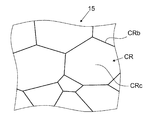
図2は、第1の実施形態に係る不揮発性記憶装置の一部の構成を例示する模式図である。
図2は、記憶層15の結晶CRを例示している。
記憶層15は、例えば、スパッタリングによって形成される。スパッタリングにおいては、上記のM1、M2、X、α及びβを含む材料をターゲットとして用いる。
FIG. 2 is a schematic view illustrating the configuration of a part of the nonvolatile memory device according to the first embodiment.
FIG. 2 illustrates the crystal CR of the
The
M1、M2、X、α及びβのうち、α及びβは、上記いずれかの結晶構造で結晶化する際に、結晶CRの粒界部CRb付近に集まる。このため、結晶CRの粒界部CRbにおけるαの濃度は、結晶CRの中心部CRcにおけるαの濃度よりも高い。また、結晶CRの粒界部CRbにおけるβの濃度は、結晶CRの中心部CRcにおけるβの濃度よりも高い。 Among M1, M2, X, α, and β, α and β gather near the grain boundary portion CRb of the crystal CR when crystallizing with any of the above crystal structures. For this reason, the concentration of α in the grain boundary portion CRb of the crystal CR is higher than the concentration of α in the center portion CRc of the crystal CR. Further, the concentration of β in the grain boundary portion CRb of the crystal CR is higher than the concentration of β in the center portion CRc of the crystal CR.
以上のような材料を記憶層15に使用することで、高い記録密度を実現しつつ、低抵抗状態と高抵抗状態との間で遷移可能な回数が増加する。例えば、スイッチング確率が向上する。スイッチング確率は、低抵抗状態と高抵抗状態との間で記憶層15を遷移させる処理を行った回数に対する、処理に応答して記憶層15が正常に遷移した回数の割合である。低抵抗状態と高抵抗状態との間の遷移は、情報の書き込み及び消去に対応している。従って、スイッチング確率が向上すると、情報の書き込み及び消去を正常に実施できるサイクル寿命が向上する。本実施形態によれば、動作安定性の高い不揮発性記憶装置が得られる。例えば、本実施形態においては、Pbpsi(Peta bit per square inch)以上の記憶密度を実現することができる。
By using the material as described above for the
以下、本実施形態に係る不揮発性記憶装置110における動作の例をモデル的に説明する。
図3は、第1の実施形態に係る不揮発性記憶装置の動作を例示する模式図である。
図3に表したように、記憶層15は、抵抗(抵抗率)が低い低抵抗状態(低抵抗状態LR)と、低抵抗状態よりも抵抗(抵抗率)が相対的に高い高抵抗状態(高抵抗状態HR)とを有する。記憶層15において、低抵抗状態LRと、高抵抗状態HRと、の間を可逆的に遷移可能である。
Hereinafter, an example of the operation in the
FIG. 3 is a schematic view illustrating the operation of the nonvolatile memory device according to the first embodiment.
As illustrated in FIG. 3, the
以下では、記憶層15の初期状態が高抵抗状態HRである場合として説明する。
記憶層15に設けられた電位勾配により、記憶層15を変化させ、記憶層15を低抵抗状態LRにすることにより情報の書き込みを行う。
Hereinafter, the case where the initial state of the
Information is written by changing the
記憶層15は、位置が固定された陽イオン(第1陽イオン51)と、移動可能な陽イオン(第2陽イオン52)と、陰イオン53と、を含む。例えば、第1陽イオン51として上記の「M1」の元素が用いられ、第2陽イオン52として上記の「M2」の元素が用いられ、陰イオン53として上記の「X」の元素が用いられる。例えば、第1陽イオン51の少なくとも一部は、遷移元素である。すなわち、第1陽イオン51の価数は変化可能である。
The
まず、例えば、第2導電部20の電位が、第1導電部10の電位よりも相対的に低い状態を作る。例えば、第1導電部10を固定電位(例えば、接地電位)とし、第2導電部20に負の電位を与える。これにより、第2陽イオン52の一部が結晶中(記憶層15の中)を第2導電部20(陰極)に向けて移動する。結晶である記憶層15の内部において、第2陽イオン52の数が、陰イオン53に対して相対的に減少する。
First, for example, a state in which the potential of the second
第2導電部20の側に移動した第2陽イオン52は、第2導電部20から電子を受取り、例えば、金属原子52mとして析出して金属層17が形成される。すなわち、記憶層15のうちで第2導電部20に近い領域では、第2陽イオン52が還元されて金属的に振る舞う。これにより、電気抵抗が減少する。
The
一方、記憶層15の内部では、陰イオン53が過剰となるため、記憶層15の内部に残された第1陽イオン51の価数が上昇する。これにより、記憶層15において、電子伝導性が発現する。その結果、記憶層15全体として、低抵抗状態LRへと変化する。この動作を、セット動作SOという。セット動作SOは、例えば書き込み動作である。
On the other hand, since the
書き込んだ情報の読み出しは、例えば電圧パルスを記憶層15に印加し、記憶層15の抵抗値を検出することにより行う。この時、電圧パルスの大きさは、記憶層15の抵抗が変化しない程度の微小な値とされる。
Reading of the written information is performed by, for example, applying a voltage pulse to the
なお、以上説明した過程は、一種の電気分解である。例えば、第1導電部10(陽極)の側では電気化学的酸化により酸化剤が生じ、第2導電部20(陰極)の側では電気化学的還元により還元剤が生じる。 The process described above is a kind of electrolysis. For example, an oxidizing agent is generated by electrochemical oxidation on the first conductive portion 10 (anode) side, and a reducing agent is generated by electrochemical reduction on the second conductive portion 20 (cathode) side.
一方、低抵抗状態LRを高抵抗状態HRに戻す動作(リセット動作RO)の際には、例えば、記憶層15に大電流パルスを印加し、それによるジュール熱によって記憶層15を加熱して、記憶層15の酸化還元反応を促進させる。ジュール熱により、第2陽イオン52は、熱的により安定な結晶構造内(記憶層15の内部)へと戻り、初期の高抵抗状態HRが現れる。リセット動作ROは、例えば消去動作である。
On the other hand, in the operation of returning the low resistance state LR to the high resistance state HR (reset operation RO), for example, a large current pulse is applied to the
また、セット動作SOとは逆極性の電圧パルスを印加してもリセット動作ROを行うことができる。例えば、第1導電部10を固定電位とし、第2導電部20に正の電位を与えることにより、第2導電部20の近傍の金属原子52mは第2導電部20に電子を与え、第2陽イオン52となる。第2陽イオン52は、記憶層15内の電位勾配により記憶層15の内部に戻る。これにより、初期の高抵抗状態HRへと変化する。
このようにして、本実施形態に係る不揮発性記憶装置110の書き込み動作及び消去動作、すなわち、セット動作SO及びリセット動作ROが行われる。
Further, the reset operation RO can be performed even when a voltage pulse having a polarity opposite to that of the set operation SO is applied. For example, by setting the first
In this way, the write operation and erase operation of the
このようなセット動作SO及びリセット動作ROが行われる不揮発性記憶装置を実用化するには、以下の2つの条件が満たされることが好ましい。1つは、室温におけるリセット動作ROが十分に抑制されることである。言い換えると、十分に長いリテンション時間を確保することである。もう1つは、リセット動作ROの消費電力が十分に小さいことである。 In order to put into practical use a nonvolatile memory device in which such a set operation SO and a reset operation RO are performed, it is preferable that the following two conditions are satisfied. One is that the reset operation RO at room temperature is sufficiently suppressed. In other words, ensuring a sufficiently long retention time. The other is that the power consumption of the reset operation RO is sufficiently small.
室温でのリセット動作ROは、例えば、第1陽イオン51及び第2陽イオン52を2価以上にすることで抑制できる。リセット動作ROの消費電力は、例えば、結晶破壊を引き起こすことなく、記憶層15内(結晶CR内)を移動する第2陽イオン52のイオン半径及び移動パスを導入することにより、小さくできる。これらの条件は、既に説明した元素及び結晶構造を有する記憶層15を用いることで、実現できる。
The reset operation RO at room temperature can be suppressed, for example, by making the
セット動作SO後の第1導電部10(陽極)側には、酸化剤が生じる。このため、第1導電部10には、酸化され難い材料を用いる。これにより、第1導電部10の酸化による不揮発性記憶装置110の劣化を防止できる。酸化され難い材料としては、例えば、電気伝導性窒化物や電気伝導性酸化物などが挙げられる。
An oxidizing agent is generated on the first conductive portion 10 (anode) side after the set operation SO. For this reason, a material that is not easily oxidized is used for the first
また、第1導電部10の材料は、イオン電導性を有しないものがよい。
酸化され難く、イオン電導性を有しない材料としては、例えば、D1N、D2Ot、D3D4O3、及び、D52D6O4などが挙げられる。
ここで、「D1」は、Ti、Zr、Hf、V、Nb及びTaよりなる群から選択された少なくともいずれかを含む。
「N」は、窒素である。
「D2」は、Ti、V、Cr、Mn、Fe、Co、Ni、Cu、Zr、Nb、Mo、Ru、Rh、Pd、Ag、Hf、Ta、W、Re、Ir、Os及びPtよりなる群から選択された少なくともいずれかを含む。
組成比tは、1≦t≦4を満たす。
「O」は、酸素である。
「D3」は、La、K、Ca、Sr、Ba及びLn(ランタノイド元素)よりなる群から選択された少なくともいずれかを含む。
「D4」は、Ti、V、Cr、Mn、Fe、Co、Ni、Cu、Zr、Nb、Mo、Ru、Rh、Pd、Ag、Hf、Ta、W、Re、Ir、Os及びPtよりなる群から選択された少なくともいずれかを含む。
「D5」は、K、Ca、Sr、Ba及びLn(ランタノイド元素)よりなる群から選択された少なくともいずれかを含む。
「D6」は、Ti、V、Cr、Mn、Fe、Co、Ni、Cu、Zr、Nb、Mo、Ru、Rh、Pd、Ag、Hf、Ta、W、Re、Ir、Os及びPtよりなる群から選択された少なくともいずれかを含む。
上記のうち、最も好ましい材料は、電気伝導率の良さなどを加味した総合的性能の観点から、LaNiO3である。
Moreover, the material of the 1st
Examples of the material that is not easily oxidized and does not have ionic conductivity include D1N, D2O t , D3D4O 3 , and D5 2 D6O 4 .
Here, “D1” includes at least one selected from the group consisting of Ti, Zr, Hf, V, Nb, and Ta.
“N” is nitrogen.
“D2” is composed of Ti, V, Cr, Mn, Fe, Co, Ni, Cu, Zr, Nb, Mo, Ru, Rh, Pd, Ag, Hf, Ta, W, Re, Ir, Os, and Pt. Including at least one selected from the group.
The composition ratio t satisfies 1 ≦ t ≦ 4.
“O” is oxygen.
“D3” includes at least one selected from the group consisting of La, K, Ca, Sr, Ba, and Ln (lanthanoid elements).
“D4” is made of Ti, V, Cr, Mn, Fe, Co, Ni, Cu, Zr, Nb, Mo, Ru, Rh, Pd, Ag, Hf, Ta, W, Re, Ir, Os, and Pt. Including at least one selected from the group.
“D5” includes at least one selected from the group consisting of K, Ca, Sr, Ba, and Ln (lanthanoid elements).
“D6” is made of Ti, V, Cr, Mn, Fe, Co, Ni, Cu, Zr, Nb, Mo, Ru, Rh, Pd, Ag, Hf, Ta, W, Re, Ir, Os, and Pt. Including at least one selected from the group.
Among the above, the most preferable material is LaNiO 3 from the viewpoint of the overall performance in consideration of good electrical conductivity and the like.
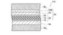
図4は、第1の実施形態に係る別の不揮発性記憶装置の構成を例示する模式図である。 図4に表したように、不揮発性記憶装置112は、ヒータ層35と、保護層33Bと、を、さらに備える。保護層33Bは、第2導電部20の上に設けられる。保護層33Bは、第2導電部20を保護する。ヒータ層35は、第2導電部20と保護層33Bとの間に設けられる。ヒータ層35は、リセット動作ROにおいて記憶層15の加熱に用いられる。これにより、リセット動作ROの際の記憶層15の酸化還元反応をより促進させることができる。保護層33Bは、第1導電部10の下に設けてもよい。ヒータ層35及び保護層33Bは、必要に応じて設けられ、省略可能である。
FIG. 4 is a schematic view illustrating the configuration of another nonvolatile memory device according to the first embodiment. As illustrated in FIG. 4, the
セット動作SOの後、記憶層15の第2導電部20側の部分には、還元剤が生じる。そこで、保護層33Bには、例えば、SnO2などの半導体、アモルファスカーボン及びダイヤモンドライクカーボンなどを用いる。これにより、セット動作SO後に記憶層15に生じた還元剤が、大気と反応することを防止できる。ヒータ層35には、例えば、約10−5Ωcm以上の抵抗率を持つ材料を用いる。
After the set operation SO, a reducing agent is generated in the portion of the
第1導電部10と記憶層15との間、または第2導電部20と記憶層15との間に、ペルチエ素子膜を設けてもよい。これにより、第1導電部10及び第2導電部20を保護しつつ、記憶層15のみを有効に加熱することができる。例えば、陽極である第1導電部10と記憶層15との間に、p型ペルチエ素子膜を設ける。p型ペルチエ素子膜は、第1導電部10から記憶層15に向けて熱を移動させる。これにより、第1導電部10の劣化を抑制しつつ、記憶層15を効率的に加熱できる。これにより、サイクル寿命、リセット確率及びリセット動作RO時の消費電力のいずれも特性が改善する。
A Peltier element film may be provided between the first
p型ペルチエ素子膜には、例えば、ペルチエ係数の大きい材料を用いる。ペルチエ係数は、ゼーベック係数と温度との積で表される。従って、p型ペルチエ素子膜には、ゼーベック係数の大きい材料を用いる。ゼーベック係数の大きい材料は、例えば、フェルミ面での状態密度が急峻になっている。また、p型ペルチエ素子膜には、例えば、ゼーベック係数が大きいとともに、強相関電子系であり、かつ低次元構造の結晶構造を有する材料を用いる。これにより、不揮発性記憶装置112の特性が、より改善される。この条件を満足する材料としては、例えば、Ca3Co4O9、LaCaCoO4、La2CuO4、CuAlO2などが挙げられる。また、p型ペルチエ素子膜の抵抗値は、記憶層15の抵抗値よりも低くする。そこで、p型ペルチエ素子膜には、上記の材料に若干p形キャリアを注入し、低抵抗化したものを用いる。これにより、ゼーベック係数は、いずれも100μV/K以上を有する。上記の材料を用いた場合、計算上において、リセット動作RO時の記憶層15の全発熱量に対して、30%〜100%の第1導電部10の冷却効果が期待される。
For the p-type Peltier element film, for example, a material having a large Peltier coefficient is used. The Peltier coefficient is represented by the product of the Seebeck coefficient and temperature. Therefore, a material having a large Seebeck coefficient is used for the p-type Peltier element film. A material having a large Seebeck coefficient has, for example, a steep state density on the Fermi surface. For the p-type Peltier element film, for example, a material having a large Seebeck coefficient, a strongly correlated electron system, and a low-dimensional crystal structure is used. Thereby, the characteristics of the
以下、記憶層15に関する材料の特性の例について説明する。
試料においては、直径が約60mmで、厚さ約1mmのガラス基板からなるディスクが用いられる。このディスクの上に、下部電極層が設けられ、下部電極層の上に記憶層15となる試料層が設けられ、その上に上部電極層及び保護層が設けられる。下部電極層及び上部電極層には、厚さが500nmのPt膜が用いられる。保護層には、ダイヤモンドライクカーボン(DLC)が用いられる。
Hereinafter, an example of material characteristics relating to the
In the sample, a disk made of a glass substrate having a diameter of about 60 mm and a thickness of about 1 mm is used. A lower electrode layer is provided on the disk, a sample layer serving as the
記憶層15となる原料を含む所定のターゲットを用い、所定の雰囲気でのRFマグネトロンスパッタにより、記憶層15が形成できる。記憶層15の形成の際のディスクの温度は300℃〜600℃の範囲内の値に維持される。記憶層15の厚さは、約10nmである。
The
上部電極層に、タングステン(W)のプローブを接触させ、記憶層15に電流を通電する。プローブの先端の径は、約10nmである。書き込み動作においては、下部電極層とプローブとの間に10ナノ秒(ns)で1ボルト(V)の電圧パルスを印加する。消去動作においては、下部電極層とプローブとの間に、100nsで0.2Vの電圧パルスを印加する。この書き込み動作と消去動作とを繰り返して実施したときに、記憶層15における高抵抗状態HRの抵抗値の、低抵抗状態LRの抵抗値に対する比(オンオフ比)が1,000以上であるときのスイッチング確率が評価値として用いられる。
A tungsten (W) probe is brought into contact with the upper electrode layer, and a current is passed through the
第1試料においては、記憶層15としてZnV2O4+0.1Li+0.1Fが用いられる。第1試料における記憶層15は、ZnV2O4+0.1Li+0.1Fの合金ターゲットを用い、95%のArと、5%のO2と、を含む雰囲気中でのRFマグネトロンスパッタにより形成される。ダイヤモンドライクカーボンは、例えば、CVD(Chemical Vapor Deposition)法により、記憶層15の上に、厚さ約3nmで形成される。
In the first sample, ZnV 2 O 4 + 0.1Li + 0.1F is used as the
第1試料に対し、10,000箇所にプローブを当てて電圧パルスの印加を実施する。第1試料では、全ての箇所において、オンオフ比1,000以上で書き込み及び消去が繰り返される。すなわち、第1試料のスイッチング確率は、100%である。また、第1試料のスイッチング回数SWNは、10,000サイクル以上である。 A voltage pulse is applied to the first sample by applying probes to 10,000 locations. In the first sample, writing and erasing are repeated at an on / off ratio of 1,000 or more at all locations. That is, the switching probability of the first sample is 100%. The switching frequency SWN of the first sample is 10,000 cycles or more.
以下の各試料において、説明しない部分は、上記の第1試料と同様である。
第2試料においては、記憶層15としてZnCr2O4+0.1Li+0.1Fが用いられる。
第3試料においては、記憶層15としてZnMn2O4+0.1Li+0.1Fが用いられる。
第4試料においては、記憶層15としてZnCo2O4+0.1Li+0.1Fが用いられる。
第5試料においては、記憶層15としてMgCr2O4+0.1Li+0.1Fが用いられる。
第6試料においては、記憶層15としてMgMn2O4+0.1Li+0.1Fが用いられる。
第7試料においては、記憶層15としてMgCo2O4+0.1Li+0.1Fが用いられる。
第8試料においては、記憶層15としてCoMn2O4+0.1Li+0.1Fが用いられる。
第9試料においては、記憶層15としてCaCr2O4+0.1Li+0.1Fが用いられる。
第10試料においては、記憶層15としてCaMn2O4+0.1Li+0.1Fが用いられる。
第11試料においては、記憶層15としてSrMn2O4+0.1Li+0.1Fが用いられる。
第12試料においては、記憶層15としてBa0.25Mn2O4+0.1Li+0.1Fが用いられる。製造方法については、Ba0.25Mn2O4+0.1Li+0.1Fをスパッタ法により形成し、Baを約10nmの厚さで形成する。
第13試料においては、記憶層15としてZn0.25Mn2O4+0.1Li+0.1Fが用いられる。製造方法については、Zn0.25Mn2O4+0.1Li+0.1Fをスパッタ法により形成し、Znを約10nmの厚さで形成する。
第14試料においては、記憶層15としてCuAlO2+0.1Li+0.1Fが用いられる。
第15試料においては、記憶層15としてMgCrO3+0.1Li+0.1Fが用いられる。
第16試料においては、記憶層15としてNiWN2+0.1Li+0.1Fが用いられる。また、保護層としてSnO2が用いられる。製造方法については、NiWN2+0.1Li+0.1FをAr95%、NH35%の雰囲気中でスパッタ法により形成する。
第17試料においては、記憶層15としてZn1.2V1.8O4+0.1Li+0.1Fが用いられる。また、保護層としてSnO2が用いられる。
第18試料においては、記憶層15としてZn1.2Cr1.8O4+0.1Li+0.1Fが用いられる。また、保護層としてSnO2が用いられる。
第19試料においては、記憶層15としてZnAl1.8Cr0.2O4+0.1Li+0.1Fが用いられる。また、保護層としてSnO2が用いられる。
第20試料においては、記憶層15としてZnAl1.8Mn0.2O4+0.1Li+0.1Fが用いられる。また、保護層としてSnO2が用いられる。
第21試料においては、記憶層15としてZnSc1.8Mn0.2O4+0.1Li+0.1Fが用いられる。また、保護層としてSnO2が用いられる。
第22試料においては、記憶層15としてZnY1.8Mn0.2O4+0.1Li+0.1Fが用いられる。また、保護層としてSnO2が用いられる。
第23試料においては、記憶層15としてZnLn1.8Mn0.2O4+0.1Li+0.1Fが用いられる。また、保護層としてSnO2が用いられる。
第24試料においては、記憶層15としてZnGa1.8Mn0.2O4+0.1Li+0.1Fが用いられる。また、保護層としてSnO2が用いられる。
第25試料においては、記憶層15としてZnAl1.8Ti0.2O4+0.1Li+0.1Fが用いられる。また、保護層としてSnO2が用いられる。
第26試料においては、記憶層15としてZnAl1.8Zr0.2O4+0.1Li+0.1Fが用いられる。また、保護層としてSnO2が用いられる。
第27試料においては、記憶層15としてZnAl1.8Hf0.2O4+0.1Li+0.1Fが用いられる。また、保護層としてSnO2が用いられる。
第28試料においては、記憶層15としてZnAl1.8Si0.2O4+0.1Li+0.1Fが用いられる。また、保護層としてSnO2が用いられる。
第29試料においては、記憶層15としてZnAl1.8Ge0.2O4+0.1Li+0.1Fが用いられる。また、保護層としてSnO2が用いられる。
第30試料においては、記憶層15としてZnAl1.8Sn0.2O4+0.1Li+0.1Fが用いられる。また、保護層としてSnO2が用いられる。
第31試料においては、記憶層15としてZnFe1.8Mn0.2O4+0.1Li+0.1Fが用いられる。また、保護層としてSnO2が用いられる。
第32試料においては、記憶層15としてZnAl1.8Nb0.2O4+0.1Li+0.1Fが用いられる。また、保護層としてSnO2が用いられる。
第33試料においては、記憶層15としてZnAl1.8Ta0.2O4+0.1Li+0.1Fが用いられる。また、保護層としてSnO2が用いられる。
第34試料においては、記憶層15としてZnAl1.8Mo0.2O4+0.1Li+0.1Fが用いられる。また、保護層としてSnO2が用いられる。
第35試料においては、記憶層15としてZnAl1.8Ru0.2O4+0.1Li+0.1Fが用いられる。また、保護層としてSnO2が用いられる。
第36試料においては、記憶層15としてZnAl1.8Rh0.2O4+0.1Li+0.1Fが用いられる。また、保護層としてSnO2が用いられる。
以上の第2〜第36試料においては、10,000箇所にプローブを当てて電圧パルスの印加を実施し、全ての箇所において、オンオフ比1,000以上で書き込み及び消去が繰り返される。すなわち、第2〜第36試料のスイッチング確率は、100%である。また、第2〜第36試料のスイッチング回数SWNは、10,000サイクル以上である。
In the following samples, the parts not described are the same as those in the first sample.
In the second sample, ZnCr 2 O 4 + 0.1Li + 0.1F is used as the
In the third sample, ZnMn 2 O 4 + 0.1Li + 0.1F is used as the
In the fourth sample, ZnCo 2 O 4 + 0.1Li + 0.1F is used as the
In the fifth sample, MgCr 2 O 4 + 0.1Li + 0.1F is used as the
In the sixth sample, MgMn 2 O 4 + 0.1Li + 0.1F is used as the
In the seventh sample, MgCo 2 O 4 + 0.1Li + 0.1F is used as the
In the eighth sample, CoMn 2 O 4 + 0.1Li + 0.1F is used as the
In the ninth sample, CaCr 2 O 4 + 0.1Li + 0.1F is used as the
In the tenth sample, CaMn 2 O 4 + 0.1Li + 0.1F is used as the
In the eleventh sample, SrMn 2 O 4 + 0.1Li + 0.1F is used as the
In the twelfth sample, Ba 0.25 Mn 2 O 4 + 0.1Li + 0.1F is used as the
In the thirteenth sample, Zn 0.25 Mn 2 O 4 + 0.1Li + 0.1F is used as the
In the fourteenth sample, CuAlO 2 + 0.1Li + 0.1F is used as the
In the fifteenth sample, MgCrO 3 + 0.1Li + 0.1F is used as the
In the sixteenth sample, NiWN 2 + 0.1Li + 0.1F is used as the
In the seventeenth sample, Zn 1.2 V 1.8 O 4 + 0.1Li + 0.1F is used as the
In the eighteenth sample, Zn 1.2 Cr 1.8 O 4 + 0.1Li + 0.1F is used as the
In the nineteenth sample, ZnAl 1.8 Cr 0.2 O 4 + 0.1Li + 0.1F is used as the
In the twentieth sample, ZnAl 1.8 Mn 0.2 O 4 + 0.1Li + 0.1F is used as the
In the twenty-first sample, ZnSc 1.8 Mn 0.2 O 4 + 0.1Li + 0.1F is used as the
In the twenty-second sample, ZnY 1.8 Mn 0.2 O 4 + 0.1Li + 0.1F is used as the
In the twenty-third sample, ZnLn 1.8 Mn 0.2 O 4 + 0.1Li + 0.1F is used as the
In the twenty-fourth sample, ZnGa 1.8 Mn 0.2 O 4 + 0.1Li + 0.1F is used as the
In the 25th sample, ZnAl 1.8 Ti 0.2 O 4 + 0.1Li + 0.1F is used as the
In the twenty-sixth sample, ZnAl 1.8 Zr 0.2 O 4 + 0.1Li + 0.1F is used as the
In the twenty-seventh sample, ZnAl 1.8 Hf 0.2 O 4 + 0.1Li + 0.1F is used as the
In the twenty-eighth sample, ZnAl 1.8 Si 0.2 O 4 + 0.1Li + 0.1F is used as the
In the 29th sample, ZnAl 1.8 Ge 0.2 O 4 + 0.1Li + 0.1F is used as the
In the 30th sample, ZnAl 1.8 Sn 0.2 O 4 + 0.1Li + 0.1F is used as the
In the 31st sample, ZnFe 1.8 Mn 0.2 O 4 + 0.1Li + 0.1F is used as the
In the thirty-second sample, ZnAl 1.8 Nb 0.2 O 4 + 0.1Li + 0.1F is used as the
In the thirty-third sample, ZnAl 1.8 Ta 0.2 O 4 + 0.1Li + 0.1F is used as the
In the 34th sample, ZnAl 1.8 Mo 0.2 O 4 + 0.1Li + 0.1F is used as the
In the thirty-fifth sample, ZnAl 1.8 Ru 0.2 O 4 + 0.1Li + 0.1F is used as the
In the thirty-sixth sample, ZnAl 1.8 Rh 0.2 O 4 + 0.1Li + 0.1F is used as the
In the above second to thirty-sixth samples, a voltage pulse is applied by applying a probe to 10,000 locations, and writing and erasing are repeated at an on / off ratio of 1,000 or more at all locations. That is, the switching probability of the second to thirty-sixth samples is 100%. Further, the switching frequency SWN of the second to thirty-sixth samples is 10,000 cycles or more.
第37試料においては、記憶層15としてZnV2O4が用いられる。
第37試料において、10,000箇所にプローブを当てて電圧パルスの印加を実施する。第37試料において、オンオフ比1,000以上で書き込み及び消去が繰り返されるのは、10,000箇所のうち、7562箇所のみである。すなわち、第37試料のスイッチング確率は、75.62%である。
In the 37th sample, ZnV 2 O 4 is used as the
In the 37th sample, a voltage pulse is applied by applying a probe to 10,000 points. In the 37th sample, writing and erasing are repeated at an on / off ratio of 1,000 or more only in 7562 out of 10,000. That is, the switching probability of the 37th sample is 75.62%.
第38試料においては、記憶層15としてZnCr2O4が用いられる。
第38試料において、10,000箇所にプローブを当てて電圧パルスの印加を実施する。第38試料において、オンオフ比1,000以上で書き込み及び消去が繰り返されるのは、10,000箇所のうち、8541箇所のみである。すなわち、第38試料のスイッチング確率は、85.41%である。
In the thirty-eighth sample, ZnCr 2 O 4 is used as the
In the thirty-eighth sample, a voltage pulse is applied by applying a probe to 10,000 points. In the thirty-eighth sample, writing and erasing are repeated at an on / off ratio of 1,000 or more at only 8541 out of 10,000. That is, the switching probability of the 38th sample is 85.41%.
第39試料においては、記憶層15としてZnMn2O4が用いられる。
第39試料において、10,000箇所にプローブを当てて電圧パルスの印加を実施する。第39試料において、オンオフ比1,000以上で書き込み及び消去が繰り返されるのは、10,000箇所のうち、9682箇所のみである。すなわち、第39試料のスイッチング確率は、96.82%である。
In the 39th sample, ZnMn 2 O 4 is used as the
In the 39th sample, a voltage pulse is applied by applying a probe to 10,000 points. In the 39th sample, writing and erasing are repeated at an on / off ratio of 1,000 or more only in 9682 out of 10,000 locations. That is, the switching probability of the 39th sample is 96.82%.
第40試料においては、記憶層15としてZnCo2O4が用いられる。
第40試料において、10,000箇所にプローブを当てて電圧パルスの印加を実施する。第40試料において、オンオフ比1,000以上で書き込み及び消去が繰り返されるのは、10,000箇所のうち、6534箇所のみである。すなわち、第40試料のスイッチング確率は、65.34%である。
In the 40th sample, ZnCo 2 O 4 is used as the
In the 40th sample, a voltage pulse is applied by applying a probe to 10,000 points. In the 40th sample, writing and erasing are repeated at an on / off ratio of 1,000 or more at only 6534 out of 10,000. That is, the switching probability of the 40th sample is 65.34%.
第41試料においては、記憶層15としてMgCr2O4が用いられる。
第41試料において、10,000箇所にプローブを当てて電圧パルスの印加を実施する。第41試料において、オンオフ比1,000以上で書き込み及び消去が繰り返されるのは、10,000箇所のうち、3766箇所のみである。すなわち、第41試料のスイッチング確率は、37.66%である。
In the forty-first sample, MgCr 2 O 4 is used as the
In the 41st sample, a voltage pulse is applied by applying a probe to 10,000 locations. In the forty-first sample, writing and erasing are repeated at an on / off ratio of 1,000 or more only in 3766 locations out of 10,000 locations. That is, the switching probability of the 41st sample is 37.66%.
第42試料においては、記憶層15としてMgMn2O4が用いられる。
第42試料において、10,000箇所にプローブを当てて電圧パルスの印加を実施する。第42試料において、オンオフ比1,000以上で書き込み及び消去が繰り返されるのは、10,000箇所のうち、3587箇所のみである。すなわち、第42試料のスイッチング確率は、35.87%である。
In the forty-second sample, MgMn 2 O 4 is used as the
In the 42nd sample, a voltage pulse is applied by applying a probe to 10,000 points. In the forty-second sample, writing and erasing are repeated at an on / off ratio of 1,000 or more at only 3587 out of 10,000. That is, the switching probability of the forty-second sample is 35.87%.
第1〜第36試料においては、記憶層15は(M11−uM2u)xX+yα+zβで表される材料である。第37〜第42試料においては、記憶層15は(M11−uM2u)xX+yα+zβで表される材料でない。このように、(M11−uM2u)xX+yα+zβで表される材料を記憶層15に用いることで、低抵抗状態と高抵抗状態との間で遷移可能な回数が増加する。すなわち、動作安定性が向上する。
In the first to thirty-sixth samples, the
本実施形態において、記憶層15に含まれる(M11−uM2u)xX+yα+zβの組成比「x」は、0.1≦x≦1.1を満たす。組成比「y」は、0.0001≦y≦0.2を満たす。組成比「z」は、0.9≦y/z≦1.1を満たす。
In the present embodiment, the composition ratio “x” of (M1 1−u M2 u ) xX + yα + zβ included in the
以下、組成比x、組成比y及び組成比zを変えたときの記憶層15の特性の例について説明する。
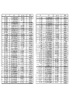
図5は、不揮発性記憶装置の特性を例示する表である。
図5には、(M11−uM2u)xX+yα+zβで表される材料において、組成比x、組成比y及び組成比zを変えたときの、スイッチング確率の判定Evを示している。ここで、記憶層15において、低抵抗状態と高抵抗状態との相互の遷移(スイッチング)を10,000箇所で実施したときに、スイッチング確率が100%の場合が、良好な特性が得られている状態である。スイッチング確率100%未満の場合は、特性が良くない状態である。
図5においては、良好な特性が得られている状態は、「判定Ev」に関して「OK」と表示されている。特性が良くない状態は、「判定Ev」に関して「NG」と表示されている。図5においては、「M1」としてZnを用い、「M2」としてMnを用い、「X」としてO(酸素)を用い、「α」としてLiを用い、「β」としてFを用いたときの例が示されている。
Hereinafter, examples of characteristics of the
FIG. 5 is a table illustrating characteristics of the nonvolatile memory device.
FIG. 5 shows determination Ev of the switching probability when the composition ratio x, the composition ratio y, and the composition ratio z are changed in the material represented by (M1 1-u M2 u ) xX + yα + zβ. Here, in the
In FIG. 5, “OK” is displayed for “determination Ev” when a good characteristic is obtained. A state where the characteristics are not good is displayed as “NG” regarding “determination Ev”. In FIG. 5, Zn is used as “M1”, Mn is used as “M2”, O (oxygen) is used as “X”, Li is used as “α”, and F is used as “β”. An example is shown.
図5から分かるように、良好な特性が得られているとき(判定Evが「OK」のとき)は、組成比xが0.1以上1.1以下である。組成比xが0.1未満、または、1.1より大きいときは、良好な特性が得られない(判定Evは「NG」)。組成比xが0.1以上1.1以下であっても、組成比yが、0.0001より小さい、または、0.2より大きいときは、良好な特性が得られない。さらに、組成比xが0.1以上1.1以下であっても、組成比yと組成比zとの比であるy/zが、0.9より小さい、または、1.1より大きいときは、良好な特性が得られない。 As can be seen from FIG. 5, when good characteristics are obtained (when the determination Ev is “OK”), the composition ratio x is 0.1 or more and 1.1 or less. When the composition ratio x is less than 0.1 or greater than 1.1, good characteristics cannot be obtained (determination Ev is “NG”). Even if the composition ratio x is 0.1 or more and 1.1 or less, when the composition ratio y is smaller than 0.0001 or larger than 0.2, good characteristics cannot be obtained. Furthermore, even when the composition ratio x is 0.1 or more and 1.1 or less, when y / z which is the ratio of the composition ratio y and the composition ratio z is smaller than 0.9 or larger than 1.1 Does not provide good characteristics.
また、図5では、「M1」がZnで、「M2」がMnで、「X」がO(酸素)で、「α」がLiで、「β」がFのときの例が示されている。「M1」及び「M2」が、Mg、Al、Sc、Y、Ga、Ti、Zr、Hf、Si、Ge、Sn、V、Cr、Mn、Fe、Co、Ni、Cu、Zn、Nb、Ta、Mo、W、Ru、Rh、Ca、Sr、Ba及びLnのいずれかであるときも、同様の傾向となる。「X」が、OまたはNであるときも、同様の傾向となる。「α」が、Na、K、Rb、Cs及びFrのいずれかであるときも、同様の傾向となる。「β」が、Cl、Br及びIのいずれかであるときも、同様の傾向となる。 FIG. 5 shows an example in which “M1” is Zn, “M2” is Mn, “X” is O (oxygen), “α” is Li, and “β” is F. Yes. “M1” and “M2” are Mg, Al, Sc, Y, Ga, Ti, Zr, Hf, Si, Ge, Sn, V, Cr, Mn, Fe, Co, Ni, Cu, Zn, Nb, Ta , Mo, W, Ru, Rh, Ca, Sr, Ba, and Ln have the same tendency. The same tendency is obtained when “X” is O or N. The same tendency is obtained when “α” is any one of Na, K, Rb, Cs, and Fr. The same tendency is obtained when “β” is any one of Cl, Br, and I.
このように、記憶層15では、(M11−uM2u)xX+yα+zβで表される材料において、組成比「x」が0.1以上1.1以下であり、組成比「y」が0.0001以上0.2以下であり、かつ組成比「y/z」が0.9以上1.1以下のときに、良好な特性が得られる。
Thus, in the
(第2の実施形態)
本実施形態に係る不揮発性記憶装置は、クロスポイント型の構成を有する。
図6は、第2の実施形態に係る不揮発性記憶装置の構成を例示する模式的斜視図である。
図7は、第2の実施形態に係る不揮発性記憶装置の構成を例示する模式図である。
図6及び図7に表したように、本実施形態に係る不揮発性記憶装置210においては、基板30が設けられる。基板30の主面に対して並行な平面をX−Y平面とする。X−Y平面内の1つの方向をX軸方向とする。X−Y平面内においてX軸方向に対して垂直な方向をY軸方向とする。X軸方向とY軸方向とに対して垂直な方向をZ軸方向とする。
(Second Embodiment)
The nonvolatile memory device according to this embodiment has a cross-point configuration.
FIG. 6 is a schematic perspective view illustrating the configuration of the nonvolatile memory device according to the second embodiment.
FIG. 7 is a schematic view illustrating the configuration of the nonvolatile memory device according to the second embodiment.
As shown in FIGS. 6 and 7, the
不揮発性記憶装置210において、基板30の主面の上に、X軸方向に延在する帯状の第1の配線(ワード線WLi−1、WLi、WLi+1)が設けられる。さらに、Y軸方向に延在する帯状の第2の配線(ビット線BLj−1、BLj、BLj+1)が、設けられる。第2の配線(ビット線BLj−1、BLj、BLj+1)は、第1の配線(ワード線WLi−1、WLi、WLi+1)に対向する。
In the
なお、上記では、第1の配線の延在方向が第2の配線の延在方向に対して直交するが、第1の配線の延在方向が第2の配線の延在方向と交差(非平行)すれば良い。 In the above description, the extending direction of the first wiring is orthogonal to the extending direction of the second wiring, but the extending direction of the first wiring intersects with the extending direction of the second wiring (non- (Parallel).
なお、上記において添え字i及び添え字jは任意である。すなわち、第1の配線の数及び第2の配線の数は、任意である。
本具体例では、第1の配線がワード線となり、第2の配線がビット線となる。ただし、第1の配線がビット線で、第2の配線がワード線でも良い。以下では、第1の配線がワード線であり、第2の配線がビット線であるとして説明する。
In the above, the suffix i and the suffix j are arbitrary. That is, the number of first wirings and the number of second wirings are arbitrary.
In this specific example, the first wiring is a word line and the second wiring is a bit line. However, the first wiring may be a bit line and the second wiring may be a word line. In the following description, it is assumed that the first wiring is a word line and the second wiring is a bit line.
図6及び図7に表したように、第1の配線と第2の配線との間にメモリセル33が設けられる。
As shown in FIGS. 6 and 7, the
図7に表したように、例えば、ワード線WLi−1、WLi、WLi+1の一端は、選択スイッチであるMOSトランジスタRSWを介して、デコーダ機能を有するワード線ドライバ31に接続される。ビット線BLj−1、BLj、BLj+1の一端は、選択スイッチであるMOSトランジスタCSWを介して、デコーダ及び読み出し機能を有するビット線ドライバ32に接続される。
As shown in FIG. 7, for example, one end of each of the word lines WL i−1 , WL i , WL i + 1 is connected to a
MOSトランジスタRSWのゲートには、ワード線(ロウ)を選択するための選択信号Ri−1、Ri、Ri+1が入力され、MOSトランジスタCSWのゲートには、ビット線(カラム)を選択するための選択信号Ci−1、Ci、Ci+1が入力される。 Selection signals R i−1 , R i , and R i + 1 for selecting a word line (row) are input to the gate of the MOS transistor RSW, and a bit line (column) is selected to the gate of the MOS transistor CSW. Selection signals C i−1 , C i , and C i + 1 are input.
メモリセル33は、ワード線WLi−1、WLi、WLi+1と、ビット線BLj−1、BLj、BLj+1と、が互いに対向する交差部に配置される。メモリセル33には、書き込み/読み出し時における回り込み電流(sneak current)を防止するための整流素子34を付加することができる。
In the
図8は、第2の実施形態に係る不揮発性記憶装置の一部の構成を例示する模式的断面図である。
図8に表したように、ワード線WLiとビット線BLjとの間には、メモリセル33及び整流素子34が設けられる。なお、ワード線WLiとビット線BLjとの上下の配置の関係は任意である。ワード線WLiとビット線BLjとの間における、メモリセル33と整流素子34との配置の順番は、任意である。
FIG. 8 is a schematic cross-sectional view illustrating the configuration of a part of the nonvolatile memory device according to the second embodiment.
As shown in FIG. 8, a
図8に表したように、メモリセル33は、記憶部22を含む。記憶部22は、第1導電部10と、第2導電部20と、第1導電部10と第2導電部20との間に設けられた記憶層15と、を含む。記憶層15には、第1の実施形態に関して説明した構成が適用できる。
As illustrated in FIG. 8, the
メモリセル33は、保護層33Bをさらに含むことができる。本具体例では、保護層33Bは、記憶部22のビット線BLjの側に設けられているが、保護層33Bは、記憶部22のワード線WLiの側に設けても良く、整流素子34とワード線WLiとの間に設けても良い。メモリセル33は、記憶部22と保護層33Bとの間に設けられたヒータ層35をさらに含むことができる。ヒータ層35及び保護層33Bは、必要に応じて設けられ、省略可能である。
The
なお、第1導電部10及び第2導電部20の少なくともいずれかとして、記憶部22に隣接する、例えば、ワード線WLi、整流素子34、ヒータ層35、保護層33B、ビット線BLjの少なくともいずれかを用いても良い。
In addition, as at least one of the first
図9及び図10は、第2の実施形態に係る別の不揮発性記憶装置の構成を例示する模式的斜視図である。
図9及び図10に表したように、本実施形態に係る不揮発性記憶装置211及び212においては、ワード線、ビット線、及び、それらの間に設けられたメモリセル33を含む積層構造体が、複数積み重ねられる。これにより、3次元構造の不揮発性記憶装置が形成される。
9 and 10 are schematic perspective views illustrating the configuration of another nonvolatile memory device according to the second embodiment.
As shown in FIGS. 9 and 10, in the
本実施形態に係る不揮発性記憶装置210、211、212においては、駆動部となるワード線ドライバ31及びビット線ドライバ32は、ワード線WLi及びビット線BLjを介して、記憶層15への電圧の印加、及び、記憶層15への電流の通電、の少なくともいずれかを行う。これにより、記憶層15に変化を発生させて情報を書き込む。例えば、駆動部は、記憶層15に電圧を印加して記憶層15に変化を発生させて情報を書き込む。また、書き込んだ情報を読み出すことができる。また、消去を行うことができる。
In the
本実施形態に係る不揮発性記憶装置210、211、212においても、動作安定性の高い不揮発性記憶装置が提供できる。
Also in the
(第3の実施の形態)
本実施形態に係る不揮発性記憶装置は、プローブメモリ型の構成を有する。
図11は、第3の実施形態に係る不揮発性記憶装置の構成を例示する模式的斜視図である。
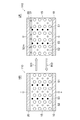
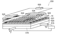
図12は、第3の実施形態に係る不揮発性記憶装置の構成を例示する模式的平面図である。
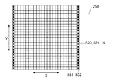
図11及び図12に表したように、本実施形態に係る不揮発性記憶装置250では、基板520と、基板520の上に設けられた電極521と、電極521の上に設けられた記憶層15(記憶媒体)と、を備える。基板520は、XYスキャナ516の上に設けられる。記憶層15には、複数のデータエリア531が設けられる。また、データエリア531のX軸方向の両端には、サーボエリア532が設けられる。
(Third embodiment)
The nonvolatile memory device according to the present embodiment has a probe memory type configuration.
FIG. 11 is a schematic perspective view illustrating the configuration of the nonvolatile memory device according to the third embodiment.
FIG. 12 is a schematic plan view illustrating the configuration of the nonvolatile memory device according to the third embodiment.
As shown in FIGS. 11 and 12, in the
記憶層15に対向するように、プローブアレイが配置される。
プローブアレイは、例えば、基板523と、基板523の一面側にアレイ状に配置される複数のプローブ(ヘッド)524と、を有する。プローブ524として、例えば、カンチレバーが用いられる。複数のプローブ524は、マルチプレクスドライバ525、526により駆動される。
複数のプローブ524は、それぞれ、基板523内のマイクロアクチュエータを用いて個別に動作可能である。また、全てをまとめて同じ動作をさせて記憶層15のデータエリア531に対してアクセスを行うこともできる。
A probe array is arranged to face the
The probe array includes, for example, a
Each of the plurality of
例えば、電極521が第1導電部10として用いられ、プローブ524が第2導電部20として用いられる。また、記憶層15の上に導電性の保護層33Bが設けられる場合は、その保護層33Bが、第2導電部20となる。
For example, the
例えば、マルチプレクスドライバ525、526を用いて、全てのプローブ524をX方向に一定周期で往復動作させ、記憶媒体(記憶層15)のサーボエリア532からY方向の位置情報を読み出す。Y方向の位置情報は、ドライバ515に転送される。
ドライバ515は、この位置情報に基づいてXYスキャナ516を駆動し、記憶層15をY方向に移動させ、記憶層15のデータエリア531とプローブ524との位置決めを行う。
両者の位置決めが完了したら、データエリア531上のプローブ524を用いてデータの書き込み、読み出しまたは消去を行う。
For example, using the
The
When the positioning of both is completed, data is written, read or erased using the
例えば、1つのデータエリア531に対応して1つのプローブ(ヘッド)524が設けられ、1つのサーボエリア532に対して1つのプローブ524が設けられる。各プローブ524は、例えばマルチプレクスドライバ525、526を介して、駆動部600に接続される。駆動部600は、それぞれのプローブ524に、情報記憶のための、電圧及び電流の少なくともいずれかを供給する。記憶層15は、プローブ524を介して与えられた電圧及び電流によって、高抵抗状態と低抵抗状態との間を遷移する。また、駆動部600は、記憶層15に記憶された高抵抗状態と低抵抗状態とを検出し、記憶された情報を読み出す。
For example, one probe (head) 524 is provided corresponding to one
このような構成の不揮発性記憶装置250は、記憶層15と、記憶層15への電圧の印加、及び、記憶層15への電流の通電、の少なくともいずれかによって、記憶層15に変化を発生させて情報を記憶する駆動部600と、を備える。不揮発性記憶装置250は、記憶層15に併設されたプローブ524をさらに備え、駆動部600は、プローブ524を介して、記憶層15の記憶単位に対して電圧の印加及び電流の通電の少なくともいずれかを行う。これにより、記憶層15に変化を発生させて情報を記憶する。
The
なお、駆動部600は、上記のドライバ515及びXYスキャナ516を含むこともでき、逆に、駆動部は、上記のドライバ515及びXYスキャナ516に含まれても良い。
Note that the driving
本実施形態に係るプローブメモリ型の不揮発性記憶装置250においても、動作安定性の高い不揮発性記憶装置が提供できる。
Also in the probe memory type
(第4の実施の形態)
本実施形態に係る不揮発性記憶装置は、フラッシュメモリ型の構成を有する。
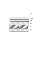
図13は、第4の実施形態に係る不揮発性記憶装置の構成を例示する模式的断面図である。
図14は、第4の実施形態に係る不揮発性記憶装置の動作を例示する模式的断面図である。
図13に表したように、本実施形態に係る不揮発性記憶装置260においては、フラッシュメモリ型のメモリセルを有する。このメモリセルは、MIS(metal-insulator-semiconductor)トランジスタの構成を有する。
(Fourth embodiment)
The nonvolatile memory device according to the present embodiment has a flash memory type configuration.
FIG. 13 is a schematic cross-sectional view illustrating the configuration of the nonvolatile memory device according to the fourth embodiment.
FIG. 14 is a schematic cross-sectional view illustrating the operation of the nonvolatile memory device according to the fourth embodiment.
As illustrated in FIG. 13, the
半導体基板41の表面領域には、複数の拡散層42が形成される。複数の拡散層42の間にチャネル領域42cが設けられる。チャネル領域42c上には、ゲート絶縁層43が形成される。ゲート絶縁層43上には、実施形態に係る記憶層15が形成される。記憶層15の上には、コントロールゲート電極45が形成される。
A plurality of diffusion layers 42 are formed in the surface region of the
記憶層15は、第1の実施形態で説明した構成を有する。例えば、チャネル領域42cが第1導電部10であり、コントロールゲート電極45が第2導電部20であると見なすことができる。また、ゲート絶縁層43と、コントロールゲート電極45との間に、第1導電部10、第2導電部20及び記憶層15を含む記憶部22が設けられても良い。以下の図においては、記憶部22を、適宜、記憶層15として省略して表示する。
The
半導体基板41は、ウェル領域でも良い。半導体基板41は、拡散層42の導電形に対して逆の導電形を有する。コントロールゲート電極45は、ワード線となる。コントロールゲート電極45には、例えば、導電性ポリシリコンが用いられる。
The
本実施形態においては、図示しない駆動部が、コントロールゲート電極45に接続されて設けられる。駆動部は、コントロールゲート電極45を介して、記憶層15への電圧の印加、及び、記憶層15への電流の通電、の少なくともいずれかを行う。
In the present embodiment, a drive unit (not shown) is provided connected to the
図14に表したように、セット(書き込み)動作SOでは、コントロールゲート電極45に電位V1を与え、半導体基板41に電位V2を与える。
電位V1及び電位V2の差は、記憶層15が変化、すなわち、抵抗が変化するのに十分な大きさである。ただし、電位の差の極性は、特に、限定されない。すなわち、V1>V2、及び、V1<V2のいずれでも良い。
As shown in FIG. 14, in the set (write) operation SO, the potential V <b> 1 is applied to the
The difference between the potential V1 and the potential V2 is large enough for the
例えば、初期状態(リセット状態)において、記憶層15が高抵抗状態HRであると仮定すると、ゲート絶縁層43が厚くなったことになるため、メモリセル(MISトランジスタ)の閾値は、高くなる。
For example, in the initial state (reset state), assuming that the
この状態から電位V1、V2を与えて記憶層15を低抵抗状態LRに変化させると、ゲート絶縁層43が薄くなったことになるため、メモリセル(MISトランジスタ)の閾値は、低くなる。
When the potentials V1 and V2 are applied from this state to change the
なお、電位V2は、半導体基板41に与えたが、これに代えて、メモリセルのチャネル領域42cに拡散層42から電位V2を転送するようにしても良い。なお、同図において、矢印Aeは電子の移動を表し、矢印Aiはイオンの移動を表している。
Although the potential V2 is applied to the
一方、リセット(消去)動作ROでは、コントロールゲート電極45に電位V1’を与え、拡散層42の一方に電位V3を与え、拡散層42の他方に電位V4(<V3)を与える。電位V1’は、セット状態のメモリセルの閾値を越える値にする。
On the other hand, in the reset (erase) operation RO, the potential V1 'is applied to the
この時、メモリセルはオンになり、電子が拡散層42の他方から一方に向かって流れると共に、ホットエレクトロンが発生する。このホットエレクトロンは、ゲート絶縁層43を介して記憶層15に注入されるため、記憶層15の温度が上昇する。
At this time, the memory cell is turned on, electrons flow from the other side of the
これにより、記憶層15は、低抵抗状態LRから高抵抗状態HRに変化するため、ゲート絶縁層43が厚くなったことになり、メモリセル(MISトランジスタ)の閾値は、高くなる。
Thereby, since the
このように、フラッシュメモリと類似した原理により、メモリセルの閾値を変えることができ、不揮発性記憶装置として利用できる。
本実施形態に係る不揮発性記憶装置260においては、記憶層15として第1の実施形態に関して説明した記憶層15を用いているので、動作安定性の高い不揮発性記憶装置が提供できる。
As described above, the threshold value of the memory cell can be changed based on a principle similar to that of the flash memory, which can be used as a nonvolatile memory device.
In the
図15は、第4の実施形態に係る別の不揮発性記憶装置の構成を例示する模式図である。
図16(a)〜図16(c)は、第4の実施形態に係る別の不揮発性記憶装置を例示する模式的断面図である。
本実施形態に係る別の不揮発性記憶装置261は、NAND型フラッシュメモリである。図15は、NANDセルユニット261cの回路図を示している。図26(a)は、NANDセルユニット261cの構造を例示している。
FIG. 15 is a schematic view illustrating the configuration of another nonvolatile memory device according to the fourth embodiment.
FIG. 16A to FIG. 16C are schematic cross-sectional views illustrating another nonvolatile memory device according to the fourth embodiment.
Another
図15に表したように、NANDセルユニット261cは、直列接続される複数のメモリセルMCからなるNANDストリングと、その両端に1つずつ接続される合計2つのセレクトゲートトランジスタSTと、を含む。
As shown in FIG. 15, the
図16(a)に表したように、p形半導体基板41a内には、n形ウェル領域41b及びp形ウェル領域41cが設けられる。p形ウェル領域41c内に、NANDセルユニット261cが形成される。
As shown in FIG. 16A, an n-
この例では、メモリセルMCは、セレクトゲートトランジスタSTと同じ構造を有する。具体的には、これらは、n形拡散層42と、n形拡散層42の間のチャネル領域42c上のゲート絶縁層43と、ゲート絶縁層43上の記憶層15と、記憶層15上のコントロールゲート電極45と、を含む。
In this example, the memory cell MC has the same structure as the select gate transistor ST. Specifically, these are the n-
図15に表したように、各コントロールゲート電極45(CG)は、駆動部600に電気的に接続される。なお、駆動部600は、NANDセルユニット261cが設けられる基板に設けられても良く、それとは別の基板に設けられても良い。
As shown in FIG. 15, each control gate electrode 45 (CG) is electrically connected to the
メモリセルMCの記憶層15の状態(高抵抗状態HR及び低抵抗状態LR)は、図14に関して説明した動作により変化させることが可能である。これに対し、セレクトゲートトランジスタSTの記憶層15は、セット状態、すなわち、低抵抗状態LRに固定される。
The state of the
セレクトゲートトランジスタSTの1つは、ソース線SLに接続され、他の1つは、ビット線BLに接続される。 One of the select gate transistors ST is connected to the source line SL, and the other one is connected to the bit line BL.
セット(書き込み)動作SOの前には、NANDセルユニット261c内の全てのメモリセルは、リセット状態(抵抗大)になっているものとする。セット(書き込み)動作SOにおいては、ソース線SL側のメモリセルMCからビット線BL側のメモリセルに向かって1つずつ順番に行われる。選択されたワード線(コントロールゲート電極)WLに書き込み電位としてV1(正電位)を与え、非選択のワード線WLに転送電位(メモリセルMCがオンになる電位)としてVpassを与える。ソース線SL側のセレクトゲートトランジスタSTをオフ、ビット線BL側のセレクトゲートトランジスタSTをオンにし、ビット線BLから選択されたメモリセルMCのチャネル領域42cにプログラムデータを転送する。
It is assumed that all memory cells in the
例えば、プログラムデータが“1”の時は、選択されたメモリセルMCのチャネル領域42cに書き込み禁止電位(例えば、V1と同じ程度の電位)を転送し、選択されたメモリセルMCの記憶層15の抵抗値が高い状態から低い状態に変化しないようにする。
For example, when the program data is “1”, a write inhibit potential (for example, the same potential as V1) is transferred to the
また、プログラムデータが“0”の時は、選択されたメモリセルMCのチャネル領域42cにV2(<V1)を転送し、選択されたメモリセルMCの記憶層15の抵抗値を高い状態から低い状態に変化させる。
When the program data is “0”, V2 (<V1) is transferred to the
一方、リセット(消去)動作ROでは、例えば、全てのワード線(コントロールゲート電極)WLにV1’を与え、NANDセルユニット261c内の全てのメモリセルMCをオンにする。また、2つのセレクトゲートトランジスタSTをオンにし、ビット線BLにV3を与え、ソース線SLにV4(<V3)を与える。
On the other hand, in the reset (erase) operation RO, for example, V1 'is applied to all the word lines (control gate electrodes) WL, and all the memory cells MC in the
この時、ホットエレクトロンがNANDセルユニット261c内の全てのメモリセルMCの記憶層15に注入されるため、NANDセルユニット261c内の全てのメモリセルMCに対して一括してリセット動作が実行される。
At this time, since hot electrons are injected into the storage layers 15 of all the memory cells MC in the
読み出し動作は、選択されたワード線(コントロールゲート電極)WLに読み出し電位(正電位)を与え、非選択のワード線(コントロールゲート電極)WLには、メモリセルMCがデータ“0”、“1”によらず必ずオンになる電位を与える。
また、2つのセレクトゲートトランジスタSTをオンにし、NANDストリングに読み出し電流を供給する。
選択されたメモリセルMCは、読み出し電位が印加されると、それに記憶されたデータの値に応じてオンまたはオフになるため、例えば、読み出し電流の変化を検出することにより、データを読み出すことができる。
In the read operation, a read potential (positive potential) is applied to the selected word line (control gate electrode) WL, and the memory cell MC receives data “0”, “1” on the unselected word line (control gate electrode) WL. A potential to be turned on without fail is given.
Further, the two select gate transistors ST are turned on to supply a read current to the NAND string.
When the read potential is applied, the selected memory cell MC is turned on or off according to the value of the data stored in the selected memory cell MC. For example, data can be read by detecting a change in the read current. it can.
図16(b)に表したように、本実施形態に係る別の不揮発性記憶装置262では、セレクトゲートトランジスタSTについては、記憶層15を設けずに、通常のMISトランジスタが用いられている。このように、セレクトゲートトランジスタSTの構造は任意である。
As shown in FIG. 16B, in another
図16(c)に表したように、本実施形態に係る別の不揮発性記憶装置263では、NANDストリングを構成する複数のメモリセルMCのゲート絶縁層がp形半導体層47に置き換えられている。
As illustrated in FIG. 16C, in another
図17は、第4の実施形態に係る別の不揮発性記憶装置の構成を例示する模式図である。
図18は、第4の実施形態に係る別の不揮発性記憶装置の構成を例示する模式的断面図である。
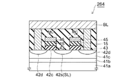
本実施形態に係る別の不揮発性記憶装置264は、NOR型フラッシュメモリである。図17は、NORセルユニット264cの回路図を示している。図18は、NORセルユニット264cの構造を例示している。
FIG. 17 is a schematic view illustrating the configuration of another nonvolatile memory device according to the fourth embodiment.
FIG. 18 is a schematic cross-sectional view illustrating the configuration of another nonvolatile memory device according to the fourth embodiment.
Another
図18に表したように、p形半導体基板41a内には、n形ウェル領域41b及びp形ウェル領域41cが形成される。p形ウェル領域41c内に、NORセルが形成される。NORセルは、ビット線BLとソース線SLとの間に接続される1つのメモリセル(MISトランジスタ)MCを含む。メモリセルMCは、n形拡散層42と、n形拡散層42の間のチャネル領域42c上のゲート絶縁層43と、ゲート絶縁層43上の記憶層15と、記憶層15上のコントロールゲート電極45と、を含む。
As shown in FIG. 18, an n-
図17に表したように、各コントロールゲート電極45(CG)は、駆動部600に電気的に接続される。なお、駆動部600は、NORセルユニット264cが設けられる基板に設けられても良く、それとは別の基板に設けられても良い。不揮発性記憶装置264においても、図14に関して説明した動作が実施される。
As shown in FIG. 17, each control gate electrode 45 (CG) is electrically connected to the
図19は、第4の実施形態に係る別の不揮発性記憶装置の構成を例示する模式図である。
図20は、第4の実施形態に係る別の不揮発性記憶装置の構成を例示する模式的断面図である。
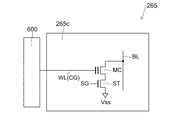
本実施形態に係る別の不揮発性記憶装置265は、2トラ型フラッシュメモリである。図19は、2トラセルユニット265cの回路図を示している。図20は、2トラセルユニット265cの構造を例示している。
FIG. 19 is a schematic view illustrating the configuration of another nonvolatile memory device according to the fourth embodiment.
FIG. 20 is a schematic cross-sectional view illustrating the configuration of another nonvolatile memory device according to the fourth embodiment.
Another
図19及び図20に表したように、2トラセルユニット265cは、NANDセルユニットの特徴とNORセルの特徴とを併せ持ったセル構造を有する。
As shown in FIGS. 19 and 20, the 2-
p形半導体基板41a内には、n形ウェル領域41b及びp形ウェル領域41cが形成される。p形ウェル領域41c内に、2トラセルユニット265cが形成される。
An n-
2トラセルユニット265cは、直列接続される1つのメモリセルMCと、1つのセレクトゲートトランジスタSTと、を含む。メモリセルMCは、セレクトゲートトランジスタSTと同じ構造を有する。具体的には、これらは、n形拡散層42と、n形拡散層42の間のチャネル領域42c上のゲート絶縁層43と、ゲート絶縁層43上の記憶層15と、記憶層15上のコントロールゲート電極45と、を含む。セレクトゲートトランジスタSTは、ソース線SLに接続され、メモリセルMCは、ビット線BLに接続される。各コントロールゲート電極45(CG)は、駆動部600に電気的に接続される。なお、駆動部600は、2トラセルユニット265cが設けられる基板に設けられても良く、それとは別の基板に設けられても良い。不揮発性記憶装置265においても、図14に関して説明した動作が実施される。
The two
図21は、第4の実施形態に係る別の不揮発性記憶装置の構成を例示する模式的断面図である。
図21に表したように、本実施形態に係る別の不揮発性記憶装置266では、セレクトゲートトランジスタSTについては、記憶層15を設けずに、通常のMISトランジスタが用いられている。このように、セレクトゲートトランジスタSTの構造は、任意である。
FIG. 21 is a schematic cross-sectional view illustrating the configuration of another nonvolatile memory device according to the fourth embodiment.
As shown in FIG. 21, in another
また、実施形態に係る不揮発性記憶装置を記憶媒体に応用しても良い。 In addition, the nonvolatile storage device according to the embodiment may be applied to a storage medium.
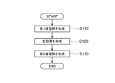
図22は、実施形態に係る不揮発性記憶装置の製造方法を例示するフローチャートである。
図22に表したように、不揮発性記憶装置110の製造方法は、第1導電部10を形成するステップS110と、第1導電部10の上に記憶層15を形成するステップS120と、記憶層15の上に第2導電部20を形成するステップS130と、を含む。
FIG. 22 is a flowchart illustrating the method for manufacturing the nonvolatile memory device according to the embodiment.
As illustrated in FIG. 22, the method for manufacturing the
ステップS120では、(M11−uM2u)xX+yα+zβで表される材料を記憶層15に用いる。
ステップS120では、上記の材料を含む記憶層15を結晶化させる。この結晶化では、α及びβの少なくとも一方を、結晶CRの粒界部CRbに集める。
また、不揮発性記憶装置110の製造方法には、ステップS120とステップS130との間に、記憶層15を洗浄するステップを、さらに含めてもよい。この洗浄では、粒界部CRbに集められたα及びβの一部が洗い流される。従って、洗浄を行った場合、記憶層15に含まれるαの量は、記憶層15の形成時に使用したαの量よりも少ない。また、洗浄を行った場合、記憶層15に含まれるβの量は、記憶層15の形成時に使用したβの量よりも少ない。
In step S <b> 120, a material represented by (M1 1-u M2 u ) xX + yα + zβ is used for the
In step S120, the
Further, the method for manufacturing the
実施形態によれば、動作安定性の高い不揮発性記憶装置及びその製造方法が提供できる。 According to the embodiment, a nonvolatile memory device with high operational stability and a method for manufacturing the same can be provided.
以上、具体例を参照しつつ、本発明の実施の形態について説明した。しかし、本発明の実施形態は、これらの具体例に限定されるものではない。例えば、不揮発性記憶装置に含まれる第1導電部、第2導電部、記憶層、陽イオン元素及び陰イオン元素などの各要素の具体的な構成に関しては、当業者が公知の範囲から適宜選択することにより本発明を同様に実施し、同様の効果を得ることができる限り、本発明の範囲に包含される。
また、各具体例のいずれか2つ以上の要素を技術的に可能な範囲で組み合わせたものも、本発明の要旨を包含する限り本発明の範囲に含まれる。
The embodiments of the present invention have been described above with reference to specific examples. However, embodiments of the present invention are not limited to these specific examples. For example, the specific configuration of each element such as the first conductive portion, the second conductive portion, the storage layer, the cation element, and the anion element included in the nonvolatile memory device is appropriately selected by those skilled in the art from a known range. By doing so, the present invention is included in the scope of the present invention as long as the same effects can be obtained and similar effects can be obtained.
Moreover, what combined any two or more elements of each specific example in the technically possible range is also included in the scope of the present invention as long as the gist of the present invention is included.
その他、本発明の実施の形態として上述した不揮発性記憶装置及びその製造方法を基にして、当業者が適宜設計変更して実施し得る全ての不揮発性記憶装置及びその製造方法も、本発明の要旨を包含する限り、本発明の範囲に属する。 In addition, on the basis of the nonvolatile memory device described above as an embodiment of the present invention and a method for manufacturing the same, all nonvolatile memory devices and methods for manufacturing the same that can be implemented by those skilled in the art as appropriate are also included in the present invention. As long as the gist is included, it belongs to the scope of the present invention.
その他、本発明の思想の範疇において、当業者であれば、各種の変更例及び修正例に想到し得るものであり、それら変更例及び修正例についても本発明の範囲に属するものと了解される。 In addition, in the category of the idea of the present invention, those skilled in the art can conceive of various changes and modifications, and it is understood that these changes and modifications also belong to the scope of the present invention. .
本発明のいくつかの実施形態を説明したが、これらの実施形態は、例として提示したものであり、発明の範囲を限定することは意図していない。これら新規な実施形態は、その他の様々な形態で実施されることが可能であり、発明の要旨を逸脱しない範囲で、種々の省略、置き換え、変更を行うことができる。これら実施形態やその変形は、発明の範囲や要旨に含まれるとともに、特許請求の範囲に記載された発明とその均等の範囲に含まれる。 Although several embodiments of the present invention have been described, these embodiments are presented by way of example and are not intended to limit the scope of the invention. These novel embodiments can be implemented in various other forms, and various omissions, replacements, and changes can be made without departing from the scope of the invention. These embodiments and modifications thereof are included in the scope and gist of the invention, and are included in the invention described in the claims and the equivalents thereof.
10…第1導電部、 15…記憶層、 17…金属層、 20…第2導電部、 22…記憶部、 30…基板、 31…ワード線ドライバ、 32…ビット線ドライバ、 33…メモリセル、 33B…保護層、 34…整流素子、 35…ヒータ層、 41…半導体基板、 41a…p形半導体基板、 41b…n形ウェル領域、 41c…p形ウェル領域、 42…拡散層(n形核酸層)、 42c…チャネル領域、 43…ゲート絶縁層、 45…コントロールゲート電極、 47…p形半導体層、 51…第1陽イオン、 52…第2陽イオン、 52m…金属原子、 53…陰イオン、 110、210、211、212、220、250、260、261〜266…不揮発性記憶装置、 261c…NANDセルユニット、 264c…NORセルユニット、 265c…2トラセルユニット、 515…ドライバ、 516…XYスキャナ、 520…基板、 521…電極、 523…基板、 524…プローブ、 525、526…マルチプレクスドライバ、 531…データエリア、 532…サーボエリア、 600…駆動部、 Ae、Ai…矢印、 BL…ビット線、 CR…結晶、 CRb…粒界部、 CRc…中心部、 HR…高抵抗状態、 LR…低抵抗状態、 MC…メモリセル、 RSW…トランジスタ、 SL…ソース線、 ST…セレクトゲートトランジスタ、 WL…ワード線
DESCRIPTION OF
Claims (8)
第2導電部と、
前記第1導電部と前記第2導電部との間に設けられ、前記第1導電部と前記第2導電部とを介して供給される電流により、抵抗が低い第1状態と前記第1状態よりも抵抗が高い第2状態との間で可逆的に遷移可能な記憶層と、
を備え、
前記記憶層は、スピネル構造、イルメナイト構造、ホランダイト構造、ウルフラマイト構造、ラムスデライト構造、デラフォサイト構造、α−NaFeO2構造、LiMoN2構造、蛍石構造、岩塩型構造、ルチル構造及びアナターゼ構造のいずれかの結晶構造を持ち、
前記記憶層は、(M11−uM2u)xX+yα+zβ(M1及びM2は、Mg、Al、Sc、Y、Ga、Ti、Zr、Hf、Si、Ge、Sn、V、Cr、Mn、Fe、Co、Ni、Cu、Zn、Nb、Ta、Mo、W、Ru、Rh、Ca、Sr、Ba及びLn(ランタノイド元素)よりなる群から選択された少なくともいずれかを含み、Xは、OまたはNの少なくともいずれかを含み、αは、Li、Na、K、Rb、Cs及びFrの少なくともいずれかを含み、βは、F、Cl、Br及びIの少なくともいずれかを含み、0.1≦x≦1.1、0.0001≦y≦0.2、0.9≦y/z≦1.1である)で表される材料を含み、
前記記憶層は、少なくとも1種の陽イオン元素と、少なくとも1種の陰イオン元素と、を含み、
前記陽イオン元素の少なくとも1種は、電子が不完全に満たされたd軌道を有する遷移元素であり、
隣接する前記陽イオン元素間の平均最短距離は、0.32nm以下であり、
前記記憶層は、結晶を含み、前記結晶の粒界部における前記αの濃度は、前記結晶の中心部における前記αの濃度よりも高い不揮発性記憶装置。 A first conductive part;
A second conductive portion;
The first state and the first state, which are provided between the first conductive unit and the second conductive unit, and have a low resistance due to a current supplied through the first conductive unit and the second conductive unit. A storage layer capable of reversibly transitioning between a second state of higher resistance than
With
The memory layer has a spinel structure, an ilmenite structure, a hollandite structure, a wolframite structure, a ramsdellite structure, a delafossite structure, an α-NaFeO 2 structure, a LiMoN 2 structure, a fluorite structure, a rock salt structure, a rutile structure, and an anatase structure. Have one of the crystal structures,
The memory layer is (M1 1-u M2 u ) xX + yα + zβ (M1 and M2 are Mg, Al, Sc, Y, Ga, Ti, Zr, Hf, Si, Ge, Sn, V, Cr, Mn, Fe, Including at least one selected from the group consisting of Co, Ni, Cu, Zn, Nb, Ta, Mo, W, Ru, Rh, Ca, Sr, Ba and Ln (lanthanoid elements), and X is O or N Α includes at least one of Li, Na, K, Rb, Cs, and Fr, β includes at least one of F, Cl, Br, and I, and 0.1 ≦ x ≦ 1.1, 0.0001 ≦ y ≦ 0.2, 0.9 ≦ y / z ≦ 1.1),
The storage layer includes at least one cation element and at least one anion element;
At least one of the cationic elements is a transition element having a d orbital incompletely filled with electrons,
The average shortest distance between adjacent cation elements is 0.32 nm or less,
The storage layer includes a crystal, and a concentration of α in a grain boundary portion of the crystal is higher than a concentration of α in a central portion of the crystal.
第2導電部と、
前記第1導電部と前記第2導電部との間に設けられ、前記第1導電部と前記第2導電部とを介して供給される電流により、抵抗が低い第1状態と前記第1状態よりも抵抗が高い第2状態との間で可逆的に遷移可能な記憶層と、
を備え、
前記記憶層は、(M11−uM2u)xX+yα+zβ(M1及びM2は、Mg、Al、Sc、Y、Ga、Ti、Zr、Hf、Si、Ge、Sn、V、Cr、Mn、Fe、Co、Ni、Cu、Zn、Nb、Ta、Mo、W、Ru、Rh、Ca、Sr、Ba及びLn(ランタノイド元素)よりなる群から選択された少なくともいずれかを含み、Xは、OまたはNの少なくともいずれかを含み、αは、Li、Na、K、Rb、Cs及びFrの少なくともいずれかを含み、βは、F、Cl、Br及びIの少なくともいずれかを含み、0.1≦x≦1.1、0.0001≦y≦0.2、0.9≦y/z≦1.1である)で表される材料を含む不揮発性記憶装置。 A first conductive part;
A second conductive portion;
The first state and the first state, which are provided between the first conductive unit and the second conductive unit, and have a low resistance due to a current supplied through the first conductive unit and the second conductive unit. A storage layer capable of reversibly transitioning between a second state of higher resistance than
With
The memory layer is (M1 1-u M2 u ) xX + yα + zβ (M1 and M2 are Mg, Al, Sc, Y, Ga, Ti, Zr, Hf, Si, Ge, Sn, V, Cr, Mn, Fe, Including at least one selected from the group consisting of Co, Ni, Cu, Zn, Nb, Ta, Mo, W, Ru, Rh, Ca, Sr, Ba and Ln (lanthanoid elements), and X is O or N Α includes at least one of Li, Na, K, Rb, Cs, and Fr, β includes at least one of F, Cl, Br, and I, and 0.1 ≦ x ≦ 1.1, 0.0001 ≦ y ≦ 0.2, 0.9 ≦ y / z ≦ 1.1).
前記陽イオン元素の少なくとも1種は、電子が不完全に満たされたd軌道を有する遷移元素であり、
隣接する前記陽イオン元素間の平均最短距離は、0.32nm以下である請求項2記載の不揮発性記憶装置。 The storage layer includes at least one cation element and at least one anion element;
At least one of the cationic elements is a transition element having a d orbital incompletely filled with electrons,
The nonvolatile memory device according to claim 2, wherein an average shortest distance between adjacent cation elements is 0.32 nm or less.
(M11−uM2u)xX+yα+zβ(M1及びM2は、Mg、Al、Sc、Y、Ga、Ti、Zr、Hf、Si、Ge、Sn、V、Cr、Mn、Fe、Co、Ni、Cu、Zn、Nb、Ta、Mo、W、Ru、Rh、Ca、Sr、Ba及びLn(ランタノイド元素)よりなる群から選択された少なくともいずれかを含み、Xは、OまたはNの少なくともいずれかを含み、αは、Li、Na、K、Rb、Cs及びFrの少なくともいずれかを含み、βは、F、Cl、Br及びIの少なくともいずれかを含み、0.1≦x≦1.1、0.0001≦y≦0.2、0.9≦y/z≦1.1である)で表される材料を用いて、抵抗が低い第1状態と前記第1状態よりも抵抗が高い第2状態との間で可逆的に遷移可能な記憶層を、前記第1導電部の上に形成し、
前記記憶層の上に、第2導電部を形成することを備えた不揮発性記憶装置の製造方法。 Forming a first conductive portion;
(M1 1-u M2 u ) xX + yα + zβ (M1 and M2 are Mg, Al, Sc, Y, Ga, Ti, Zr, Hf, Si, Ge, Sn, V, Cr, Mn, Fe, Co, Ni, Cu , Zn, Nb, Ta, Mo, W, Ru, Rh, Ca, Sr, Ba, and Ln (lanthanoid element), and X is at least one of O and N And α includes at least one of Li, Na, K, Rb, Cs, and Fr, β includes at least one of F, Cl, Br, and I, and 0.1 ≦ x ≦ 1.1, 0.0001 ≦ y ≦ 0.2, 0.9 ≦ y / z ≦ 1.1), and a first state having a low resistance and a resistance having a higher resistance than the first state. A storage layer capable of reversibly transitioning between two states on the first conductive portion. Formed,
A non-volatile memory device manufacturing method comprising forming a second conductive portion on the memory layer.
Priority Applications (2)
| Application Number | Priority Date | Filing Date | Title |
|---|---|---|---|
| JP2012068498A JP2013201280A (en) | 2012-03-24 | 2012-03-24 | Nonvolatile memory device and method of manufacturing the same |
| US13/779,716 US8816318B2 (en) | 2012-03-24 | 2013-02-27 | Nonvolatile memory device and method for manufacturing same |
Applications Claiming Priority (1)
| Application Number | Priority Date | Filing Date | Title |
|---|---|---|---|
| JP2012068498A JP2013201280A (en) | 2012-03-24 | 2012-03-24 | Nonvolatile memory device and method of manufacturing the same |
Publications (1)
| Publication Number | Publication Date |
|---|---|
| JP2013201280A true JP2013201280A (en) | 2013-10-03 |
Family
ID=49210916
Family Applications (1)
| Application Number | Title | Priority Date | Filing Date |
|---|---|---|---|
| JP2012068498A Pending JP2013201280A (en) | 2012-03-24 | 2012-03-24 | Nonvolatile memory device and method of manufacturing the same |
Country Status (2)
| Country | Link |
|---|---|
| US (1) | US8816318B2 (en) |
| JP (1) | JP2013201280A (en) |
Families Citing this family (4)
| Publication number | Priority date | Publication date | Assignee | Title |
|---|---|---|---|---|
| JP2013110279A (en) * | 2011-11-21 | 2013-06-06 | Toshiba Corp | Nonvolatile memory device |
| CN107785564B (en) * | 2017-10-18 | 2020-11-24 | 武汉理工大学 | VTi2.6O7.7Nanoparticles, preparation and use |
| US10840259B2 (en) | 2018-08-13 | 2020-11-17 | Sandisk Technologies Llc | Three-dimensional memory device including liner free molybdenum word lines and methods of making the same |
| CN112289931A (en) * | 2020-10-30 | 2021-01-29 | 深圳先进技术研究院 | Preparation method of memristor, memristor and memory device |
Family Cites Families (3)
| Publication number | Priority date | Publication date | Assignee | Title |
|---|---|---|---|---|
| EP1343154B1 (en) | 2002-03-05 | 2006-10-25 | Mitsubishi Kagaku Media Co., Ltd. | Phase-change recording material used for an information recording medium and an information recording medium employing it |
| US7733684B2 (en) | 2005-12-13 | 2010-06-08 | Kabushiki Kaisha Toshiba | Data read/write device |
| JP2007250876A (en) | 2006-03-16 | 2007-09-27 | Ricoh Co Ltd | Phase-change nonvolatile memory element, semiconductor memory and data processing system |
-
2012
- 2012-03-24 JP JP2012068498A patent/JP2013201280A/en active Pending
-
2013
- 2013-02-27 US US13/779,716 patent/US8816318B2/en active Active
Also Published As
| Publication number | Publication date |
|---|---|
| US8816318B2 (en) | 2014-08-26 |
| US20130248807A1 (en) | 2013-09-26 |
Similar Documents
| Publication | Publication Date | Title |
|---|---|---|
| JP5351144B2 (en) | Information recording / reproducing device | |
| JP4791948B2 (en) | Information recording / reproducing device | |
| JP5216847B2 (en) | Information recording / reproducing device | |
| JP4792107B2 (en) | Information recording / reproducing device | |
| JP4908555B2 (en) | Information recording / reproducing device | |
| US8089796B2 (en) | Information recording and reproducing device | |
| JP4792007B2 (en) | Information recording / reproducing device | |
| JP4792006B2 (en) | Information recording / reproducing device | |
| JP4792010B2 (en) | Information recording / reproducing device | |
| JP2008276905A (en) | Information recording and reproducing device | |
| US9000410B2 (en) | Nonvolatile memory device | |
| JP2013201280A (en) | Nonvolatile memory device and method of manufacturing the same | |
| JP5318107B2 (en) | Information recording / reproducing device | |
| JP4792125B2 (en) | Information recording / reproducing device | |
| JP4792108B2 (en) | Information recording / reproducing device | |
| WO2009116139A1 (en) | Information recording/reproducing device | |
| JP2008276904A (en) | Information recording and reproducing apparatus | |
| JP2012138512A (en) | Information recording/reproducing apparatus | |
| JP5306363B2 (en) | Information recording / reproducing device | |
| JP2008251107A (en) | Information recording/reproducing device | |
| JP2008251126A (en) | Information recording and reproducing device |