JP2013197340A - Manufacturing method of semiconductor light-emitting element wafer, semiconductor light-emitting element wafer, and susceptor - Google Patents
Manufacturing method of semiconductor light-emitting element wafer, semiconductor light-emitting element wafer, and susceptor Download PDFInfo
- Publication number
- JP2013197340A JP2013197340A JP2012063417A JP2012063417A JP2013197340A JP 2013197340 A JP2013197340 A JP 2013197340A JP 2012063417 A JP2012063417 A JP 2012063417A JP 2012063417 A JP2012063417 A JP 2012063417A JP 2013197340 A JP2013197340 A JP 2013197340A
- Authority
- JP
- Japan
- Prior art keywords
- semiconductor
- growth
- layer
- electrode
- emitting element
- Prior art date
- Legal status (The legal status is an assumption and is not a legal conclusion. Google has not performed a legal analysis and makes no representation as to the accuracy of the status listed.)
- Pending
Links
Images


Abstract
Description
本発明は、半導体発光素子ウェハの製造方法、半導体発光素子ウェハ、及びサセプタに関する。 The present invention relates to a method for manufacturing a semiconductor light emitting element wafer, a semiconductor light emitting element wafer, and a susceptor.
従来、半導体発光素子の製造工程は大きく3つに分かれている。第1は半導体成長工程であり、第2は半導体プロセス工程であり、第3はパッケージ工程である。先ず、半導体成長工程では、GaN系半導体の場合には結晶成長基板にサファイア、Si,SIC等のウェハ材料を用いて気相成長法で結晶成長が行われる。結晶成長によって成長基板上には、例えば、特許文献1に示されているように、Ga(x)Al(1-x)Nからなるバッファ層と、Siをドープしたn型クラッド層と、In(x)Ga(1-x)Nよりなる活性層と、Mgをドープしたp型クラッド層とからなる発光素子の半導体構造層が形成される。 Conventionally, the manufacturing process of a semiconductor light emitting device is roughly divided into three. The first is a semiconductor growth step, the second is a semiconductor process step, and the third is a package step. First, in the semiconductor growth process, in the case of a GaN-based semiconductor, crystal growth is performed by a vapor phase growth method using a wafer material such as sapphire, Si, or SIC as a crystal growth substrate. On the growth substrate by crystal growth, for example, as shown in Patent Document 1, a buffer layer made of Ga (x) Al (1-x) N, an n-type cladding layer doped with Si, and In A semiconductor structure layer of a light-emitting element is formed which includes an active layer made of (x) Ga (1-x) N and a p-type cladding layer doped with Mg.
半導体プロセス工程では、成長基板上の半導体構造層に対してp型電極形成、n型電極形成、素子分割、光取出し構造形成などの工程が行われ、これにより発光素子本体が製造される。 In the semiconductor process, processes such as p-type electrode formation, n-type electrode formation, element division, and light extraction structure formation are performed on the semiconductor structure layer on the growth substrate, thereby manufacturing the light-emitting element body.
パッケージ工程では、発光素子本体に対して配線、蛍光体塗布、樹脂封止などの工程が行われ、発光素子の製品形状が作製される。 In the packaging process, processes such as wiring, phosphor coating, resin sealing, and the like are performed on the light emitting element body, and the product shape of the light emitting element is manufactured.
これらの半導体成長工程、半導体プロセス工程、及びパッケージ工程の各工程で検査工程が必要になる。半導体成長工程から半導体プロセス工程までの検査工程で代表的な例として、PL検査工程(フォトルミネッセンス・マッピング(PL-mapping:Photoluminescence-mapping))検査工程、顕微鏡検察工程、及び全数点灯検査工程がある。 An inspection process is required in each of these semiconductor growth processes, semiconductor process processes, and package processes. Typical examples of inspection processes from the semiconductor growth process to the semiconductor process process include the PL inspection process (PL-mapping: Photoluminescence-mapping) inspection process, the microscopic inspection process, and the 100% lighting inspection process. .
PL検査工程は、半導体成長直後の検査工程で最も一般的であり、光の照射によって活性層を選択励起させ活性層に異常がないかを検査する工程と、光の干渉を利用した膜厚に異常がないかを検査する工程からなる。PL検査工程は最も初期段階でできる検査工程である。PL検査の目的は後工程に不良が多いウェハを流さないことである。しかしながら、PL検査工程によって不良と判断される要因全てを特定できるわけではない。よって、特定できない要因からなる不良を持つウェハは後工程へ流れてしまう。 The PL inspection process is the most common in the inspection process immediately after the growth of the semiconductor. The active layer is selectively excited by light irradiation to inspect whether the active layer is normal, and the film thickness using light interference is used. It consists of a process to check for abnormalities. The PL inspection process is an inspection process that can be performed at the earliest stage. The purpose of the PL inspection is not to flow a wafer with many defects in the subsequent process. However, not all factors that are judged to be defective by the PL inspection process can be specified. Therefore, a wafer having a defect due to an unspecified factor flows to a subsequent process.
顕微鏡観察工程では、半導体成長直後に顕微鏡によって半導体構造層の表面状態を観察し、PL検査では発見できないような小さなピットや、非発光部を探し出すことが行われる。また、例えば、半導体プロセス工程の電極形成時にパターニング(patterning)したレジストが、次工程で不良の原因とならないように洗浄されているかを顕微鏡により目視検査する。上記のように顕微鏡観察工程は各工程間の検査で用いられており、ウェハの不良を発見する目的で行うというよりは各工程が正常に行われたかの確認に用いる。よって、顕微鏡観察工程においても不良の要因全てを特定できるわけではないので、特定できない要因からなる不良を持つウェハは後工程へ流れてしまう。 In the microscope observation step, the surface state of the semiconductor structure layer is observed with a microscope immediately after the growth of the semiconductor to find small pits and non-light emitting portions that cannot be found by the PL inspection. Further, for example, it is visually inspected by a microscope whether a resist patterned at the time of forming an electrode in a semiconductor process step is cleaned so as not to cause a defect in the next step. As described above, the microscope observation process is used in the inspection between the processes, and is used for confirming whether each process is normally performed rather than for the purpose of finding a defect of the wafer. Therefore, not all factors of defects can be specified even in the microscope observation process, and therefore wafers having defects due to factors that cannot be specified flow to the subsequent process.
全数点灯検査工程では、成長基板を残して全ての発光素子が電極形成、素子分割されている状態で点灯検査することが行われる。この全数点灯検査工程では不良部分が検出されるとその不良部分は除去される。発光素子の電流電圧特性(I−V特性)を簡易的に検査することができるので、不良の検査工程としては半導体発光素子の製造段階において、最も信頼性が高い検査工程である。 In the 100% lighting inspection process, a lighting inspection is performed in a state where all the light emitting elements are formed with electrodes and divided into elements, leaving the growth substrate. In this 100% lighting inspection process, when a defective portion is detected, the defective portion is removed. Since the current-voltage characteristic (IV characteristic) of the light emitting element can be easily inspected, the defect inspection process is the most reliable inspection process in the manufacturing stage of the semiconductor light emitting element.
このように半導体発光素子の製造工程においては様々な検査工程があり、後工程へ不良のものをできるだけ流さないように検査が組まれている。 As described above, there are various inspection processes in the manufacturing process of the semiconductor light emitting device, and inspection is set up so that defective ones are not passed as much as possible to the subsequent processes.
しかしながら、最も信頼性の高い全数点灯検査は半導体製造工程の最終工程に近い段階で行うことになる。 However, the most reliable 100% lighting inspection is performed at a stage close to the final process of the semiconductor manufacturing process.
従来技術の問題点は、半導体成長工程の終了直後に半導体プロセス工程ヘウェハを供給する際の不良検出工程にある。 The problem with the prior art lies in the defect detection process when a wafer is supplied to the semiconductor process process immediately after the semiconductor growth process is completed.
例えば、特許文献1や特許文献2に示されている発光素子を製造する場合に、半導体成長工程直後に、不良検出工程として先ずPL検査が行われる。このPL検査で把握できることは、(1)発光波長がどの程度であるか、(2)活性層不良による非発光部の発見、(3)全層の総膜厚の3つである。よって、上記3つに当てはまる不良であれば、半導体成長工程の終了直後のPL検査でウェハの異常を検出でき、後工程へ不良が流れない。しかしながら、不良となる要因は、活性層不良だけではない。例えば、n型クラッド層及びp型クラッド層の不良はPL検査で把握することはできない。クラッド層の不良とは、例えば、n型ドーパント(Si)やp型ドーパント(Mg)が想定濃度でドーピングされていないことや、クラッド層の結晶性低下などがある。また、各層の相互作用による不良なども考えられる。 For example, when manufacturing the light emitting element shown in Patent Document 1 or Patent Document 2, a PL inspection is first performed as a defect detection process immediately after the semiconductor growth process. There are three things that can be grasped by this PL inspection: (1) what is the emission wavelength, (2) discovery of a non-light emitting portion due to defective active layer, and (3) total film thickness of all layers. Therefore, if the defect is applicable to the above three, the abnormality of the wafer can be detected by the PL inspection immediately after the completion of the semiconductor growth process, and the defect does not flow to the subsequent process. However, the cause of failure is not only the failure of the active layer. For example, defects in the n-type cladding layer and the p-type cladding layer cannot be grasped by the PL inspection. The defect of the cladding layer includes, for example, that the n-type dopant (Si) and the p-type dopant (Mg) are not doped at an assumed concentration, and the crystallinity of the cladding layer is lowered. Moreover, the defect by interaction of each layer etc. can also be considered.
PL検査では把握できないこれらの不良に対して、更に専用の検査工程を挿入することも可能である。例えば、ドーパント濃度検査には、ホール測定や2次イオン質量分析(SIMS:Secondary Ion Mass Spectrometry)、キャリア濃度分析(ECV:Electrochemical Capacitance Voltage)などを用いればよい。また、結晶性検査には、X線回折(XRD:X-ray defraction)を用いればよい。しかしながら、これらの分析の全てを行うことは現実的に不可能である。なぜならば、各工程において各分析に必要な準備時間、分析時間、解析時間などがあるため、大幅なコストアップに繋がる。また、分析によっては破壊試験になり、分析を行った後、半導体プロセス工程に回すことができない。 It is also possible to insert a dedicated inspection process for these defects that cannot be grasped by the PL inspection. For example, for the dopant concentration inspection, hole measurement, secondary ion mass spectrometry (SIMS), carrier concentration analysis (ECV), or the like may be used. For crystallinity inspection, X-ray diffraction (XRD) may be used. However, it is practically impossible to perform all of these analyses. This is because the preparation time, analysis time, analysis time and the like necessary for each analysis in each process lead to a significant cost increase. Moreover, depending on the analysis, it becomes a destructive test, and after performing the analysis, it cannot be sent to the semiconductor process step.
更に、各層の相互作用による不良については、原因を究明する方法が多岐にわたりすぎるため、各要因を究明するために多くの分析装置が必要になってしまう。 Furthermore, since there are too many ways to determine the cause of defects due to the interaction between layers, many analyzers are required to determine each factor.
よって、半導体プロセス工程の終盤の全数点灯検査まで不良に気づかずに流してしまう要因は決して少なくなく、半導体成長段階での不良はウェハ単位となるため、大量の不良が後工程に流れることになる。 Therefore, there are not a few factors that cause a failure to be noticed until the final lighting test in the final stage of the semiconductor process is performed, and defects in the semiconductor growth stage are in units of wafers, so a large number of defects flow to the subsequent process. .
結局のところ、半導体発光素子の目的が点灯することである以上、不良の原因が何であれ、最も確実に不良であるかないかを判断できる方法は、点灯検査である。よって、半導体発光素子の製造工程の早い段階で、点灯検査を行うことが最も不良を後工程に流さない方法である。 After all, as long as the purpose of the semiconductor light-emitting element is to turn on, the lighting inspection is the most reliable method for determining whether a failure is caused or not. Therefore, performing the lighting inspection at an early stage of the manufacturing process of the semiconductor light emitting element is a method for preventing the most defects from being passed to the subsequent process.
そこで、半導体成長工程の終了直後にこれらの不良を発見できるように簡易的に点灯試験を行えるようにしようとした場合に、半導体成長工程の終了直後には、成長基板上にn型クラッド層と、活性層と、p型クラッド層が積層された半導体構造層であるので、p型電極は露出したp型クラッド層上に簡単に形成できるが、n型クラッド層は露出していないため、n型電極を形成することができない。n型電極を露出させる場合、ドライエッチング装置などの装置を用いてp型クラッド層及び活性層を除去しなければならないので検査工程を増やすだけでなく、p型クラッド層、活性層の除去工程(レジスト塗布、ドライエッチング)n型電極及びp型電極の形成という新工程を組み込まなければならなくなる。不良の早期発見によるコストダウンを目的とした検査工程を入れることによって工数が増加し、コストアップに繋がりかねない。 Therefore, when an attempt is made to perform a lighting test simply so that these defects can be found immediately after the completion of the semiconductor growth process, an n-type cladding layer is formed on the growth substrate immediately after the completion of the semiconductor growth process. Since the active layer and the p-type cladding layer are laminated semiconductor layers, the p-type electrode can be easily formed on the exposed p-type cladding layer, but the n-type cladding layer is not exposed. A mold electrode cannot be formed. When the n-type electrode is exposed, the p-type cladding layer and the active layer must be removed using an apparatus such as a dry etching apparatus, so that not only the inspection process is increased, but also the removal process of the p-type cladding layer and the active layer ( A new process of forming an n-type electrode and a p-type electrode must be incorporated. By introducing an inspection process aimed at reducing costs by early detection of defects, man-hours increase, which may lead to cost increases.
そこで、本発明の目的は、かかる点を鑑みてなされたものであり、半導体発光素子の製造工程の早い段階にしかも低コストで全数点灯検査を行うことができる半導体発光素子ウェハの製造方法、半導体発光素子ウェハ、及びサセプタを提供することである。 Accordingly, an object of the present invention has been made in view of the above points, and a method for manufacturing a semiconductor light-emitting element wafer and a semiconductor capable of performing a complete lighting inspection at an early stage of the manufacturing process of the semiconductor light-emitting element at low cost A light emitting device wafer and a susceptor are provided.
本発明の半導体発光素子ウェハの製造方法は、基板上に、第1導電型を有する第1半導体層、活性層、及び第2導電型を有する第2半導体層をその順に積層して半導体構造層を形成する半導体成長工程を有する半導体発光素子ウェハの製造方法であって、前記半導体成長工程において、前記基板上の一部領域で前記半導体構造層の成長温度より低温にて異常成長させて前記第1半導体層の少なくとも一部が露出した異常成長部を生成し、前記半導体成長工程の終了後に、前記異常成長部以外の正常成長部の前記第2半導体層上に第1電極を形成し、前記異常成長部から露出した前記第1半導体層に接続された第2電極を形成する電極形成工程を含むことを特徴としている。 According to the method of manufacturing a semiconductor light emitting device wafer of the present invention, a first semiconductor layer having a first conductivity type, an active layer, and a second semiconductor layer having a second conductivity type are stacked in that order on a substrate. A method of manufacturing a semiconductor light emitting device wafer having a semiconductor growth step of forming a semiconductor substrate, wherein in the semiconductor growth step, the first region is abnormally grown at a temperature lower than a growth temperature of the semiconductor structure layer in a partial region on the substrate. Forming an abnormally grown portion in which at least a part of one semiconductor layer is exposed, and forming a first electrode on the second semiconductor layer of a normally grown portion other than the abnormally grown portion after the completion of the semiconductor growth step; It includes an electrode forming step of forming a second electrode connected to the first semiconductor layer exposed from the abnormally grown portion.
本発明の半導体発光素子ウェハは、表面に、第1導電型を有する第1半導体層、活性層、及び第2導電型を有する第2半導体層がその順に成長形成された半導体構造層を有する半導体発光素子ウェハであって、前記半導体構造層は前記表面の一部領域に前記半導体構造層の成長温度より低温の成長温度で異常成長された前記第1半導体層の少なくとも一部が露出した異常成長部を含み、前記異常成長部以外の正常成長部の前記第2半導体層上に配置された第1電極と、前記異常成長部から露出した前記第1半導体層上に配置された第2電極と、を有することを特徴としている。 The semiconductor light emitting device wafer of the present invention has a semiconductor structure layer on the surface of which a first semiconductor layer having a first conductivity type, an active layer, and a second semiconductor layer having a second conductivity type are grown and formed in that order. The light emitting device wafer, wherein the semiconductor structure layer is abnormally grown in which at least a part of the first semiconductor layer that is abnormally grown at a growth temperature lower than a growth temperature of the semiconductor structure layer is exposed in a partial region of the surface A first electrode disposed on the second semiconductor layer in a normal growth portion other than the abnormal growth portion, and a second electrode disposed on the first semiconductor layer exposed from the abnormal growth portion, It is characterized by having.
本発明のサセプタは、半導体成長のために基板を搭載するサセプタであって、前記基板の搭載面側の一部に前記基板への熱伝導率の低い低熱伝導部を有することを特徴としている。 The susceptor of the present invention is a susceptor on which a substrate is mounted for semiconductor growth, and has a low thermal conductivity portion having a low thermal conductivity to the substrate on a part of the mounting surface side of the substrate.
本発明の半導体発光素子ウェハの製造方法によれば、半導体成長工程において、基板上の一部領域で半導体構造層の成長温度より低温にて異常成長させて第1半導体層の少なくとも一部が露出した異常成長部を生成し、半導体成長工程の終了後に、異常成長部以外の正常成長部の第2半導体層上に第1電極を形成し、異常成長部から露出した第1半導体層に接続された第2電極を形成するので、第1電極と第2電極との間に電流を供給することによりウェハ上の発光素子の点灯検査を行うことができ、また、半導体発光素子の製造工程の早い段階に低コストでウェハ上の発光素子の全数点灯検査を行うことができる。 According to the method for manufacturing a semiconductor light emitting device wafer of the present invention, in the semiconductor growth process, at least a part of the first semiconductor layer is exposed by abnormal growth at a temperature lower than the growth temperature of the semiconductor structure layer in a partial region on the substrate. After the semiconductor growth process is completed, a first electrode is formed on the second semiconductor layer of the normal growth portion other than the abnormal growth portion, and is connected to the first semiconductor layer exposed from the abnormal growth portion. Since the second electrode is formed, lighting inspection of the light emitting element on the wafer can be performed by supplying a current between the first electrode and the second electrode, and the manufacturing process of the semiconductor light emitting element is quick. It is possible to inspect all of the light emitting elements on the wafer at a low cost.
また、本発明の半導体発光素子ウェハによれば、半導体構造層は表面の一部領域に半導体構造層の成長温度より低温の成長温度で異常成長された第1半導体層の少なくとも一部が露出した異常成長部を含み、異常成長部以外の正常成長部の第2半導体層上に配置された第1電極と、異常成長部から露出した第1半導体層上に配置された第2電極と、を有するので、第1電極と第2電極との間に電流を供給することによりウェハ上の発光素子の点灯検査を行うことができる。また、このような半導体発光素子ウェハを用いれば半導体発光素子の製造工程の早い段階に低コストで全数点灯検査を行うことができる。 According to the semiconductor light emitting device wafer of the present invention, at least a part of the first semiconductor layer abnormally grown at a growth temperature lower than the growth temperature of the semiconductor structure layer is exposed in a partial region of the semiconductor structure layer. A first electrode disposed on the second semiconductor layer of the normal growth portion other than the abnormal growth portion, including the abnormal growth portion, and a second electrode disposed on the first semiconductor layer exposed from the abnormal growth portion, Therefore, the lighting inspection of the light emitting element on the wafer can be performed by supplying a current between the first electrode and the second electrode. Further, if such a semiconductor light emitting element wafer is used, it is possible to perform a complete lighting inspection at a low cost at an early stage of the manufacturing process of the semiconductor light emitting element.
本発明のサセプタによれば、基板の搭載面側の一部に基板への熱伝導率の低い低熱伝導部を有するので、半導体成長工程において本サセプタを用いて基板上に、第1導電型を有する第1半導体層、活性層、及び第2導電型を有する第2半導体層をその順に積層して発光素子の半導体構造層を形成する場合に、半導体成長工程において基板上の一部領域で半導体構造層の成長温度より低温にて異常成長させて第1半導体層の少なくとも一部が露出した異常成長部を生成することができる。半導体成長工程の終了後に、異常成長部以外の正常成長部の第2半導体層上に第1電極を形成し、異常成長部から露出した第1半導体層に第2電極を形成して第1電極と第2電極との間に電流を供給することにより発光素子の点灯検査を行うことができ、また、発光素子の製造工程の早い段階に低コストで全数点灯検査を行うことができる。 According to the susceptor of the present invention, the first conductivity type is formed on the substrate by using the susceptor in the semiconductor growth process because the susceptor has a low thermal conductivity portion having a low thermal conductivity to the substrate on a part of the mounting surface side of the substrate. When a semiconductor structure layer of a light emitting element is formed by sequentially stacking a first semiconductor layer having an active layer and a second semiconductor layer having a second conductivity type in that order, the semiconductor is partially formed on the substrate in the semiconductor growth process. Abnormal growth at which at least a part of the first semiconductor layer is exposed can be generated by abnormal growth at a temperature lower than the growth temperature of the structural layer. After completion of the semiconductor growth process, the first electrode is formed on the second semiconductor layer in the normal growth portion other than the abnormal growth portion, and the second electrode is formed on the first semiconductor layer exposed from the abnormal growth portion. By supplying a current between the first electrode and the second electrode, it is possible to perform a lighting inspection of the light emitting element, and it is possible to perform a total lighting lighting inspection at a low cost at an early stage of the manufacturing process of the light emitting element.
以下、本発明の実施例を図面を参照しつつ詳細に説明する。 Hereinafter, embodiments of the present invention will be described in detail with reference to the drawings.
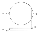
図1は実施例の製造方法の半導体成長工程で用いられる半導体成長装置を示している。半導体成長装置はサセプタ11及び加熱器12を備えている。サセプタ11はカーボンからなり、成長基板20を上面に搭載するディスク状の台座である。加熱器12はサセプタ11の下面側に配置され、サセプタ11を介して成長基板20を加熱する。
FIG. 1 shows a semiconductor growth apparatus used in the semiconductor growth process of the manufacturing method of the embodiment. The semiconductor growth apparatus includes a
図2(a)はサセプタ11の上面、すなわち成長基板20を搭載する搭載面を示し、図2(b)はサセプタ11の側面を示している。サセプタ11は図1及び図2(a),(b)に示すように、成長基板20の搭載面側外周部に段差部13を有している。段差部13はサセプタ11の外周から半径方向に0.5〜1.0mmであり、搭載面から0.1〜1.0μmの深さを有している。段差部13は成長基板20に接触しない部分となり、その成長基板20の非接触部分の成長温度を、サセプタ11の段差部13以外の成長基板20の通常の成長温度より20℃以上低くさせるために形成されている。この段差部13は基板20への熱伝導率の低い低熱伝導部に相当する。
FIG. 2A shows the upper surface of the
成長基板20は、サファイア基板等の基板であり、絶縁性及び透光性を有する。また、成長基板20は複数の発光素子分の半導体構造層を形成することができる領域を有している。
The
半導体成長工程では、図1に示した半導体成長装置を用いて、図3に示すように、成長基板20上にMOCVD(有機金属化学気相成長)法を用いて窒化ガリウム(GaN)系半導体からなる半導体構造層の正常成長部21と、正常成長部21と隣接して異常成長部22とを有する半導体発光素子ウェハが形成される。正常成長部21はサセプタ11の搭載面の段差部13以外の部分に対応した成長部分であり、通常の成長温度で正常に成長された部分である。異常成長部22は搭載面の段差部13に対応した成長部分であり、上記したように通常の成長温度より20℃以上低い成長温度で異常成長した部分である。
In the semiconductor growth process, using the semiconductor growth apparatus shown in FIG. 1, as shown in FIG. 3, a gallium nitride (GaN) based semiconductor is grown on the
正常成長部21には成長基板20側から、n型クラッド層25(第1半導体層)、多重量子井戸構造の活性層26、及びp型クラッド層27(第2半導体層)がその順に積層され、半導体構造層が形成される。一方、異常成長部22は、正常成長部21の成長温度より低温での成長により、異常成長部22では異常成長のn型クラッド層25、活性層26、及びp型クラッド層27が形成される。ただし、それら異常成長のn型クラッド層25、活性層26、及びp型クラッド層27間の境界は図3では破線で示しているが、明確ではない場合もある。また、異常成長部22の表面は凹凸面となっており、異常成長部22のn型クラッド層25の一部は、図3に露出部28として示したように露出している。
An n-type cladding layer 25 (first semiconductor layer), an
半導体構造層の具体的な形成方法としては、例えば、先ず、成長基板20が上記のMOCVD法の半導体成長装置に搬入され、1000℃の水素雰囲気中で約10分程度の加熱処理が施される。続いて、雰囲気温度が約500℃に調整され、TMG(トリメチルガリウム)(流量:10.4μmol/min)及びNH3(流量:3.3LM)が約3分間供給されることで、低温バッファ層(図示せず)が形成される。その後、雰囲気温度が約1000℃まで昇温され、かかる状態が約30秒間保持されることで低温バッファ層が結晶化される。続いて、雰囲気温度が約1000℃の状態に保持されたままで、TMG(流量:45μmol/min)及びNH3(流量:4.4LM)が約20分間供給されることにより、膜厚約1μm程度の下地GaN層13が形成される。次に、雰囲気温度が約1000℃の状態において、TMG(流量:45μmol/min)、NH3(流量:4.4LM)及びドーパントガスとしてSiH4(流量:2.7×10-9mol/min)が約100分間供給されることにより、膜厚約5μm程度のn型クラッド層25であるn型GaN層が形成される。
As a specific method for forming the semiconductor structure layer, for example, first, the
続いて、n型クラッド層25上に活性層26である多重量子井戸構造のInGaN/GaN層が形成される。活性層26ではInGaN/GaNを1周期として5周期の成長が行われる。具体的には、雰囲気温度が約700℃の状態において、TMG(流量:3.6μmol/min)、TMI(トリメチルインジウム)(流量:10μmol/min)、NH3(流量4.4LM)が約33秒間供給されることにより、膜厚約2.2nmのInGaN井戸層が形成される。続いて、TMG(流量:3.6μmol/min)、NH3(流量:4.4LM)が約320秒間供給されることにより、膜厚約15nmのGaN障壁層が形成される。かかる処理を5周期分繰り返すことにより活性層26が形成される。
Subsequently, an InGaN / GaN layer having a multiple quantum well structure as the
次に、雰囲気温度が約800℃まで昇温され、TMG(流量:8.1μmol/min)、TMA(トリメチルアルミニウム)(流量:7.5μmol/min)、NH3(流量:4.4LM)及びドーパントとしてCp2Mg(ビスシクロペンタディエニルマグネシウム:bis-cyclopentadienyl Mg)(流量:2.9×10⁻⁷μmol/min)が約5分間供給されることにより、膜厚約40nmのp型AlInGaN層(図示せず)が形成される。続いて、雰囲気温度が約800℃の状態に保持されたままで、TMG(流量:18μmol/min)、NH3(流量:4.4LM)及びドーパントとしてCp2Mg(流量:2.9×10-7μmol/min)が約7分間供給されることにより、膜厚約150nmのp型クラッド層27であるp型GaN層が形成される。
Next, the ambient temperature was raised to about 800 ° C., TMG (flow rate: 8.1 μmol / min), TMA (trimethylaluminum) (flow rate: 7.5 μmol / min), NH 3 (flow rate: 4.4 LM) and Cp as a dopant. 2 Mg (bis-cyclopentadienyl magnesium) (flow rate: 2.9 × 10 −7 μmol / min) is supplied for about 5 minutes, so that a p-type AlInGaN layer (not shown) having a film thickness of about 40 nm is formed. ) Is formed. Subsequently, while maintaining the ambient temperature at about 800 ° C., TMG (flow rate: 18 μmol / min), NH 3 (flow rate: 4.4 LM) and Cp 2 Mg as a dopant (flow rate: 2.9 × 10 −7 μmol / min) min) is supplied for about 7 minutes, whereby a p-type GaN layer which is a p-
半導体成長工程の終了後には電極形成工程が実行される。電極形成工程では、図4(a)〜(c)に示すように、正常成長部21のp型クラッド層27上に発光素子単位でp電極31(第1電極)が形成され、また、異常成長部22の凹凸面を埋めるようにn電極32(第2電極)が形成され、これによりn電極32はn型クラッド層25の露出部28上に接触する。なお、図4(a)は電極形成工程時の半導体構造層の上面図であり、図4(b)は図4(a)のX−X部分の断面図であり、図4(c)は図4(b)の異常成長部22の断面拡大図である。
After completion of the semiconductor growth process, an electrode formation process is performed. In the electrode formation step, as shown in FIGS. 4A to 4C, a p-electrode 31 (first electrode) is formed on the p-
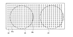
これらの電極31,32の形成には、図5に示すような金属マスク35を用いた抵抗加熱蒸着法が用いられる。金属マスク35にはp電極用の貫通孔35aとn電極用の貫通孔35bが複数のウェハ分だけ形成されている。電極31,32には、Ni(膜厚100μm程度)/Au(膜厚100μm程度)電極を用いることができる。NiはGaN結晶とのコンタクトをとるために使用され、Auは、Niの酸化防止及びプローブ(図6の符号42,43)との接触抵抗を下げるために使用される。なお、金属マスク35は図5に示すように、複数枚のウェハ(すなわち上記の成長基板20を複数枚)に同時に電極形成できるようにすることにより電極形成工程を更に効率化することができる。
The
電極形成後、図6に示すように、複数のp電極31各々に対して異常成長部22に形成したn電極32を共通のn電極として使用して点灯検査工程が行われる。点灯検査工程では、複数のp電極31とその共通のn電極32との間に電流が電源装置41から供給される。また、その電源装置41からの電流供給のために電極31,32との接続のためにプローブ42,43が用いられる。
After the electrode formation, as shown in FIG. 6, a lighting inspection process is performed using the
上記した半導体成長工程において形成された正常成長部21に形成されたGaN系半導体発光素子のp型クラッド層27は、nクラッド層25に対して電気抵抗が非常に大きく、特に、積層方向に垂直な方向には電流が流れない。このため、p型クラッド層27の側面にn電極32が接触していても、図6に電流経路Aで示すように、p型クラッド層27で電流は拡散せず、活性層26を通りnクラッド層25で電流拡散するので、異常成長部22の共通のn電極32を使用することが可能である。よって、このようにp電極31のみが発光素子単位で別々の場合でも電流はp型クラッド層27内で拡散しないため、正常成長部21において発光素子単位で正常な半導体構造層であればp電極31の直下の活性層26が発光する。各p電極31の直下の活性層26の発光状態は成長基板20側から観測される。このようにして発光素子単位で発光の特性を評価することができるので、半導体プロセス工程の終盤で行う半導体発光素子全点灯検査と同等の検査を半導体成長工程直後に電極31,32を形成するだけで行うことができる。
The p-
なお、点灯検査工程では成長基板20上の全ての発光素子分の点灯検査を行うことに限らず、一部の発光素子の点灯検査を行うだけでも良い。また、発光素子単位で点灯検査に限らず、例えば、複数の発光素子に対応した半導体構造層の領域単位でp電極31を形成して点灯を検査しても良い。
In the lighting inspection process, the lighting inspection for all the light emitting elements on the
点灯検査工程後、p電極31及びn電極32は、王水洗浄することにより除去される(電極除去工程)。その後、通常の半導体プロセス工程、そしてパッケージ工程に移行することができる。
After the lighting inspection process, the
なお、n電極32を形成した異常成長部22の表面は凹凸面であるため、王水洗浄でも電極を完全に取り除くことは困難であるが、異常成長部22はその後の素子分割工程で不要なエリアとなるため、n電極32の残渣があっても後工程への悪影響は全くない。
Since the surface of the abnormally grown
このように、半導体成長工程の終了後であって半導体プロセス工程の実行前に、上記の電極形成工程と点灯検査工程とを実行することにより、半導体成長工程の終了直後に従来のPL検査等の検査で不良と判断することが困難であった半導体発光素子ウェハを後工程の半導体プロセス工程へ流すことがなくなる。また、上記の点灯検査は非破壊検査であるので、点灯検査工程後の半導体発光素子ウェハをそのまま半導体プロセス工程で半導体発光素子製造に用いることができる。 As described above, by performing the electrode formation process and the lighting inspection process after the semiconductor growth process and before the semiconductor process process, the conventional PL inspection or the like immediately after the semiconductor growth process is completed. The semiconductor light emitting element wafer, which has been difficult to determine as defective in the inspection, is no longer passed to the subsequent semiconductor process step. Further, since the above lighting inspection is a non-destructive inspection, the semiconductor light emitting element wafer after the lighting inspection process can be used as it is for the production of a semiconductor light emitting element in the semiconductor process step.
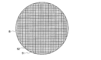
また、異常成長部22としてはウェハにおいて発光素子領域として用いられていない領域が利用されている。図7はウェハ51の発光素子の領域取りを示しており、符号52で示す□が1つの発光素子の領域である。発光素子の各領域52より外周側の領域Bは発光素子が通常形成できない領域である。そのような外周領域を異常成長部22に用いるので、最終的な半導体発光素子の取り数の減少は起こらない。
Further, as the
図8は従来の半導体発光素子の製造方法における全数点灯検査工程の状態を示している。この全数点灯検査工程は、成長基板61上で発光素子毎にp型電極形成、n型電極形成、及び素子分割が半導体プロセス工程において行われた後に実行される。図8においては、成長基板61上にはn型クラッド層62、活性層63、及びp型クラッド層64がその順に積層され2つの発光素子分の半導体構造層が形成され、各半導体構造層のn型クラッド層62上にはn電極65が形成され、p型クラッド層64上にはp電極66が形成されている。図8の全数点灯検査工程では発光素子単位でn電極65とp電極66との間にプローブ(図示せず)を用いて電流が電源装置(図示せず)から供給される。発光素子毎にn電極65とp電極66との間には図8に電流経路Cで示すように電流が流れ、これにより活性層63が発光するか否かが検査される。
FIG. 8 shows the state of the 100% lighting inspection process in the conventional method for manufacturing a semiconductor light emitting device. This 100% lighting inspection process is performed after p-type electrode formation, n-type electrode formation, and element division are performed in the semiconductor process for each light emitting element on the
この従来の半導体発光素子の製造方法における全数点灯検査工程は、半導体プロセス工程においてp型電極形成、n型電極形成、及び素子分割が行われた終盤でなければ不可能であることに対し、実施例に示した点灯検査工程は半導体成長工程の終了直後に実行でき、しかも従来の全数点灯検査工程と同様にウェハ上の全ての発光素子の発光の良否を検査することができる。半導体成長工程における通常の検査工程で検出できなかったウェハ全体の不良に関しては、従来においては半導体プロセス工程の終盤までは不良ウェハが分からずにそのまま製造を進めることになるが、実施例の製造方法では全製造工程のうちの半導体成長工程の終了直後のような早期の段階で不良ウェハを判断することができる。よって、実施例に示した点灯検査工程を実行することにより半導体成長工程終了した状態の不良ウェハを半導体プロセス工程に移行させなくて済む。 The total number lighting inspection process in this conventional method for manufacturing a semiconductor light emitting device can only be performed at the final stage in which the p-type electrode formation, the n-type electrode formation, and the element division are performed in the semiconductor process. The lighting inspection process shown in the example can be executed immediately after the completion of the semiconductor growth process, and in addition, the light emitting quality of all the light emitting elements on the wafer can be inspected in the same manner as the conventional 100% lighting inspection process. With respect to defects in the entire wafer that could not be detected in the normal inspection process in the semiconductor growth process, conventionally, the defective wafer is not recognized until the final stage of the semiconductor process process, but the manufacturing process proceeds according to the embodiment. Then, it is possible to determine a defective wafer at an early stage such as immediately after the completion of the semiconductor growth process in all the manufacturing processes. Therefore, it is not necessary to transfer the defective wafer in the state where the semiconductor growth process is completed to the semiconductor process process by executing the lighting inspection process shown in the embodiment.
更に、実施例の製造方法では、上記した電源装置41からの電極31又は32を流れる電流や素子毎の電極31,32間の電圧を測定することにより簡易的なI−V特性やウェハ面内のばらつき特性も把握することが可能になり、特性の悪いウェハをはじくことも可能になる。
Further, in the manufacturing method of the embodiment, a simple IV characteristic or in-wafer plane can be obtained by measuring the current flowing through the
また、従来、半導体成長工程の終了直後に全数点灯検査工程を行うためにはnクラッド層を露出させてn電極を設けなければならない。半導体成長工程の終了直後に例えば、レジスト塗布工程、フォトリソグラフィー工程、レジスト形成工程、ドライエッチング工程、レジスト洗浄工程、電極形成工程、全数点灯検査、及び電極除去洗浄工程を組み込まねばならない。しかしながら、このような数多くの工程を組み込むことはコストアップが回避不能である。これに対し、実施例に示した製造方法においては、n電極を設けるために半導体成長工程においてn型クラッド層25が露出した異常成長部22が形成されるので、従来のn電極を設けるための多数の工程(上記例のレジスト塗布工程からレジスト洗浄工程まで)が不必要となり、低コスト化を図ることができる。
Further, conventionally, in order to perform the complete lighting inspection process immediately after the completion of the semiconductor growth process, it is necessary to expose the n cladding layer and provide the n electrode. Immediately after the completion of the semiconductor growth process, for example, a resist coating process, a photolithography process, a resist forming process, a dry etching process, a resist cleaning process, an electrode forming process, a total lighting inspection, and an electrode removal cleaning process must be incorporated. However, it is inevitable to increase the cost by incorporating such many processes. On the other hand, in the manufacturing method shown in the embodiment, since the abnormally grown
なお、上記した実施例では、異常成長部22を形成するためにサセプタ11に、低熱伝導部として段差部13を設けて段差部13に対応した成長基板20の部分の温度を20度以上低下させているが、本発明において異常成長部22を形成する方法はこれに限定されず、成長基板20の搭載面側の一部に例えば、成長基板20への熱伝導率の低い部材によって構成された低熱伝導部を有するなど、基板の一部の成長温度が他の部分より低温となるように構成されたサセプタであれば良い。また、成長基板20の異常成長部を形成させるべき領域の下面に段差部や溝部を設けても良い。
In the above-described embodiment, the
上記した実施例においては、成長基板20側から、n型クラッド層25、活性層26、p型クラッド層27がその順に積層されたGaN系半導体構造層が示されたが、本発明はGaN系半導体構造層に限定されず、他の結晶系、例えば、GaAs系等の他の結晶系の半導体構造層でも適用することができる。また、上記した実施例においては、第1導電型をn型とし、その第1導電型とは反対導電型の第2導電型をp型としたが、本発明は第1導電型をp型とし、第2導電型をn型とした半導体構造層でも適用することができる。すなわち、本発明においては、成長基板上に、第1導電型を有する第1半導体層、活性層、及び第2導電型を有する第2半導体層をその順に積層して複数の発光素子分の半導体構造層を形成する半導体成長工程を有する半導体発光素子であれば適用することができ、半導体発光素子の製造工程の早い段階にしかも低コストで全数点灯検査を行うことができる。
In the above-described embodiment, the GaN-based semiconductor structure layer in which the n-
20,61 成長基板
21 正常成長部
22 異常成長部
25,62 n型クラッド層
26,63 活性層
27,64 p型クラッド層
28 露出部
31,66 p電極
32,65 n電極
20, 61
Claims (10)
前記半導体成長工程において、前記基板上の一部領域で前記半導体構造層の成長温度より低温にて異常成長させて前記第1半導体層の少なくとも一部が露出した異常成長部を生成し、
前記半導体成長工程の終了後に、前記異常成長部以外の正常成長部の前記第2半導体層上に第1電極を形成し、前記異常成長部から露出した前記第1半導体層に接続された第2電極を形成する電極形成工程を含むことを特徴とする製造方法。 A semiconductor light emitting device wafer having a semiconductor growth step in which a semiconductor structure layer is formed by sequentially stacking a first semiconductor layer having a first conductivity type, an active layer, and a second semiconductor layer having a second conductivity type on a substrate. A manufacturing method of
In the semiconductor growth step, an abnormal growth portion in which at least a part of the first semiconductor layer is exposed by abnormal growth at a temperature lower than a growth temperature of the semiconductor structure layer in a partial region on the substrate is generated,
After completion of the semiconductor growth step, a first electrode is formed on the second semiconductor layer in a normal growth portion other than the abnormal growth portion, and a second electrode connected to the first semiconductor layer exposed from the abnormal growth portion is formed. The manufacturing method characterized by including the electrode formation process which forms an electrode.
前記第1導電型はn型であり、前記第2導電型はp型であることを特徴とする請求項1記載の製造方法。 The semiconductor structure layer is a GaN (gallium nitride) based semiconductor structure layer,
The manufacturing method according to claim 1, wherein the first conductivity type is n-type and the second conductivity type is p-type.
前記半導体構造層は前記表面の一部領域に前記半導体構造層の成長温度より低温の成長温度で異常成長された前記第1半導体層の少なくとも一部が露出した異常成長部を含み、
前記異常成長部以外の正常成長部の前記第2半導体層上に配置された第1電極と、
前記異常成長部から露出した前記第1半導体層上に配置された第2電極と、を有することを特徴とする半導体発光素子ウェハ。 A semiconductor light emitting device wafer having a semiconductor structure layer on a surface of which a first semiconductor layer having a first conductivity type, an active layer, and a second semiconductor layer having a second conductivity type are grown and formed in that order;
The semiconductor structure layer includes an abnormally grown portion in which at least a part of the first semiconductor layer that is abnormally grown at a growth temperature lower than the growth temperature of the semiconductor structure layer is exposed in a partial region of the surface;
A first electrode disposed on the second semiconductor layer in a normal growth portion other than the abnormal growth portion;
And a second electrode disposed on the first semiconductor layer exposed from the abnormally grown portion.
前記第1導電型はn型であり、前記第2導電型はp型であることを特徴とする請求項6記載の半導体発光素子ウェハ。 The semiconductor structure layer is a GaN (gallium nitride) based semiconductor structure layer,
The semiconductor light-emitting element wafer according to claim 6, wherein the first conductivity type is n-type and the second conductivity type is p-type.
前記基板の搭載面側の一部に前記基板への熱伝導率の低い低熱伝導部を有することを特徴とするサセプタ。 A susceptor for mounting a substrate for semiconductor growth,
A susceptor comprising a low thermal conductivity portion having a low thermal conductivity to the substrate on a part of the mounting surface side of the substrate.
Priority Applications (1)
| Application Number | Priority Date | Filing Date | Title |
|---|---|---|---|
| JP2012063417A JP2013197340A (en) | 2012-03-21 | 2012-03-21 | Manufacturing method of semiconductor light-emitting element wafer, semiconductor light-emitting element wafer, and susceptor |
Applications Claiming Priority (1)
| Application Number | Priority Date | Filing Date | Title |
|---|---|---|---|
| JP2012063417A JP2013197340A (en) | 2012-03-21 | 2012-03-21 | Manufacturing method of semiconductor light-emitting element wafer, semiconductor light-emitting element wafer, and susceptor |
Publications (1)
| Publication Number | Publication Date |
|---|---|
| JP2013197340A true JP2013197340A (en) | 2013-09-30 |
Family
ID=49395921
Family Applications (1)
| Application Number | Title | Priority Date | Filing Date |
|---|---|---|---|
| JP2012063417A Pending JP2013197340A (en) | 2012-03-21 | 2012-03-21 | Manufacturing method of semiconductor light-emitting element wafer, semiconductor light-emitting element wafer, and susceptor |
Country Status (1)
| Country | Link |
|---|---|
| JP (1) | JP2013197340A (en) |
Cited By (1)
| Publication number | Priority date | Publication date | Assignee | Title |
|---|---|---|---|---|
| KR20220075118A (en) * | 2020-11-27 | 2022-06-07 | 한국생산기술연구원 | Micro LED repair method using Laser Induced Breakdown Spectroscopy and system using the same |
Citations (5)
| Publication number | Priority date | Publication date | Assignee | Title |
|---|---|---|---|---|
| JPH11220165A (en) * | 1998-01-30 | 1999-08-10 | Toshiba Corp | Manufacture of semiconductor light emitting element |
| JP2004356167A (en) * | 2003-05-27 | 2004-12-16 | Seiko Epson Corp | Method of growing crystal, method of manufacturing semiconductor laser, and crystal growing device |
| JP2011009503A (en) * | 2009-06-26 | 2011-01-13 | Sumitomo Electric Ind Ltd | Device mounted wafer, device chip, and method of manufacturing the device chip |
| JP2011114123A (en) * | 2009-11-26 | 2011-06-09 | Stanley Electric Co Ltd | Optical semiconductor device |
| JP2011192899A (en) * | 2010-03-16 | 2011-09-29 | Stanley Electric Co Ltd | Method of manufacturing semiconductor element |
-
2012
- 2012-03-21 JP JP2012063417A patent/JP2013197340A/en active Pending
Patent Citations (5)
| Publication number | Priority date | Publication date | Assignee | Title |
|---|---|---|---|---|
| JPH11220165A (en) * | 1998-01-30 | 1999-08-10 | Toshiba Corp | Manufacture of semiconductor light emitting element |
| JP2004356167A (en) * | 2003-05-27 | 2004-12-16 | Seiko Epson Corp | Method of growing crystal, method of manufacturing semiconductor laser, and crystal growing device |
| JP2011009503A (en) * | 2009-06-26 | 2011-01-13 | Sumitomo Electric Ind Ltd | Device mounted wafer, device chip, and method of manufacturing the device chip |
| JP2011114123A (en) * | 2009-11-26 | 2011-06-09 | Stanley Electric Co Ltd | Optical semiconductor device |
| JP2011192899A (en) * | 2010-03-16 | 2011-09-29 | Stanley Electric Co Ltd | Method of manufacturing semiconductor element |
Cited By (2)
| Publication number | Priority date | Publication date | Assignee | Title |
|---|---|---|---|---|
| KR20220075118A (en) * | 2020-11-27 | 2022-06-07 | 한국생산기술연구원 | Micro LED repair method using Laser Induced Breakdown Spectroscopy and system using the same |
| KR102449144B1 (en) * | 2020-11-27 | 2022-10-04 | 한국생산기술연구원 | Micro LED repair method using Laser Induced Breakdown Spectroscopy and system using the same |
Similar Documents
| Publication | Publication Date | Title |
|---|---|---|
| KR102140789B1 (en) | Evaluating apparatus for quality of crystal, and Apparatus and method for manufacturing semiconductor light emitting device which include the same | |
| JP5752855B2 (en) | Method for manufacturing light emitting device | |
| US20130032836A1 (en) | N-type gallium-nitride layer having multiple conductive intervening layers | |
| JP5740532B2 (en) | Light emitting device and manufacturing method thereof | |
| WO2014045883A1 (en) | Led element, and production method therefor | |
| TW201310698A (en) | Laterally contacted blue LED with superlattice current spreading layer | |
| JP2014524675A (en) | Light emitting device and manufacturing method thereof | |
| US20130032846A1 (en) | Non-reactive barrier metal for eutectic bonding process | |
| US20150228848A1 (en) | Nitride semiconductor light-emitting element and method for producing same | |
| TW201546903A (en) | Semiconductor light-emitting element and method for manufacturing same | |
| JP5143214B2 (en) | Semiconductor light emitting device | |
| WO2014045882A1 (en) | Led element, and production method therefor | |
| JP2014078711A (en) | Light emission diode and manufacturing method of the same | |
| US20140235005A1 (en) | Method of producing p-type nitride semiconductor and method of manufacturing nitride semiconductor light emitting device therewith | |
| JP2013197340A (en) | Manufacturing method of semiconductor light-emitting element wafer, semiconductor light-emitting element wafer, and susceptor | |
| Gujrati et al. | Multiple Shapes Micro‐LEDs with Defect Free Sidewalls and Simple Liftoff and Transfer Using Selective Area Growth on Hexagonal Boron Nitride Template | |
| US20120061715A1 (en) | Semiconductor light-emitting device manufacturing method and semiconductor light-emitting device | |
| TWI585993B (en) | Nitride light emitting device and manufacturing method thereof | |
| KR100849737B1 (en) | Light emitting diode device and manufacturing method thereof | |
| US9218967B2 (en) | Method for separating epitaxial layer from growth substrate | |
| US20120122258A1 (en) | Method for manufacturing semiconductor light emitting device | |
| JP2012238835A (en) | Semiconductor light-emitting element, and method of manufacturing wafer and semiconductor light-emitting element | |
| JP5379843B2 (en) | Semiconductor light emitting device | |
| KR101101954B1 (en) | Vertical structured group n-type nitride-based semiconductors having electrode structures with diffusion barrier, and light emitting diodes comprising said semiconductors | |
| JP5694476B2 (en) | Semiconductor light emitting device |
Legal Events
| Date | Code | Title | Description |
|---|---|---|---|
| A621 | Written request for application examination |
Free format text: JAPANESE INTERMEDIATE CODE: A621 Effective date: 20150312 |
|
| A131 | Notification of reasons for refusal |
Free format text: JAPANESE INTERMEDIATE CODE: A131 Effective date: 20151215 |
|
| A977 | Report on retrieval |
Free format text: JAPANESE INTERMEDIATE CODE: A971007 Effective date: 20151216 |
|
| A521 | Written amendment |
Free format text: JAPANESE INTERMEDIATE CODE: A523 Effective date: 20160202 |
|
| A521 | Written amendment |
Free format text: JAPANESE INTERMEDIATE CODE: A821 Effective date: 20160202 |
|
| A131 | Notification of reasons for refusal |
Free format text: JAPANESE INTERMEDIATE CODE: A131 Effective date: 20160412 |
|
| A02 | Decision of refusal |
Free format text: JAPANESE INTERMEDIATE CODE: A02 Effective date: 20161108 |