JP2013113631A - Current detector - Google Patents
Current detector Download PDFInfo
- Publication number
- JP2013113631A JP2013113631A JP2011258040A JP2011258040A JP2013113631A JP 2013113631 A JP2013113631 A JP 2013113631A JP 2011258040 A JP2011258040 A JP 2011258040A JP 2011258040 A JP2011258040 A JP 2011258040A JP 2013113631 A JP2013113631 A JP 2013113631A
- Authority
- JP
- Japan
- Prior art keywords
- magnetic
- bus bar
- current
- sensor
- detection device
- Prior art date
- Legal status (The legal status is an assumption and is not a legal conclusion. Google has not performed a legal analysis and makes no representation as to the accuracy of the status listed.)
- Pending
Links
Images


Landscapes
- Measuring Instrument Details And Bridges, And Automatic Balancing Devices (AREA)
Abstract
Description
本発明は、磁束密度や磁界の強さを検出することで導電体に流れる電流の検出を行う電流検出装置に関する。 The present invention relates to a current detection device that detects a current flowing in a conductor by detecting a magnetic flux density and a magnetic field strength.
従来、バッテリーのターミナルに接続されたハーネスに流れる電流から発生する磁束を検出することにより、バッテリーと車輌電装品との間を流れる電流値を検出することができる電流検出装置が知られている。この電流検出装置は、ブラケット等の治具を用いて車輌の一部に取り付けられている。この電流検出装置の検出孔に前記ハーネスを挿通させることにより、その部分で磁束が検出される。 2. Description of the Related Art Conventionally, there is known a current detection device that can detect a current value flowing between a battery and a vehicle electrical component by detecting a magnetic flux generated from a current flowing in a harness connected to a battery terminal. The current detection device is attached to a part of the vehicle using a jig such as a bracket. By inserting the harness through the detection hole of the current detection device, the magnetic flux is detected at that portion.
しかしながら、従来の電流検出装置においては、電流検出器を車輌に取り付けるために、ブラケット等の別体の部品を用いる必要がある。このため、部品点数が増加し構成が複雑であった。さらに、可撓性を有するハーネスを検出孔に通す必要があるので、作業性の問題から検出孔を大きくする必要がある。このため、電流検出装置の小型化を図ることが難しかった。 However, in the conventional current detection device, it is necessary to use a separate part such as a bracket in order to attach the current detector to the vehicle. For this reason, the number of parts increased and the configuration was complicated. Furthermore, since it is necessary to pass a flexible harness through the detection hole, it is necessary to enlarge the detection hole from the viewpoint of workability. For this reason, it has been difficult to reduce the size of the current detection device.
そこで、小型化を図るとともに、組立作業性を向上させ、しかも構成が簡単な車輌用電流検出装置が提案されている(例えば、特許文献1参照)。この電流検出装置は、図10に示すように、バッテリー100のターミナル101に、バスバー200の一端201をネジ102で締付けて接続させているとともに、電流検出器300をバスバー200に支持させている。また、バスバー200の他端202は、車輌電装品(図示しない)と接続されているハーネス400の端部をかみ締めているターミナル401とネジ402により連結されている。
Therefore, a vehicle current detection device has been proposed that is downsized, improves assembly workability, and has a simple configuration (see, for example, Patent Document 1). As shown in FIG. 10, in this current detection device, one
また、この電流検出器300には、図11に示すように、合成樹脂製の検出器本体301内において、バスバー200が貫通する検出孔304を包囲するように磁性体のコア302が固定されており、そのコア302の両端間に位置するようにホール素子303が実装されている。これにより、車輌用電流検出装置を簡単に構成できるとともに、小型化を実現でき、さらに組立作業性の向上を図ることもできる。
In addition, as shown in FIG. 11, a
さらに、例えば特許文献2に記載のような、電流検出装置も提案されている。図12に示すように、この電流検出装置500は、センサ自身の検出精度が高く、かつ隣接するバスバー等、外部からの磁気干渉を避けることができるようにしたコアレス電流センサで構成されている。
Furthermore, a current detection device as described in Patent Document 2, for example, has also been proposed. As shown in FIG. 12, the
即ち、この電流検出装置500は、磁気干渉を避けてコアレス電流センサを用いるために、バスバーBUに装着される磁気シールド501と、バスバーBVに装着される磁気シールド502と、バスバーBWに装着される磁気シールド503とを備えている。
That is, this
磁気シールドについては、隣接するバスバーに装着されているコアレス電流センサへの磁気干渉を低減させるために固有の配置を採用している。すなわち、平行に配置されたバスバーBU,BVおよびBWの上において、電流センサSU,SV,SWは各バスバーに沿って交互にずれた位置に配設されている。一方、磁気シールドも、同様に各バスバーに沿って交互にずれた位置に配置されている。換言すれば、この磁気シールドと電流センサの配置はいわゆる千鳥格子配置となっているわけである。 The magnetic shield employs a unique arrangement in order to reduce magnetic interference with the coreless current sensor mounted on the adjacent bus bar. That is, on the bus bars BU, BV, and BW arranged in parallel, the current sensors SU, SV, and SW are arranged at positions shifted alternately along the bus bars. On the other hand, the magnetic shields are similarly arranged at positions shifted alternately along each bus bar. In other words, the arrangement of the magnetic shield and the current sensor is a so-called staggered arrangement.
しかしながら、特許文献1に記載の電流検出装置は、下記のような不都合を生じていた。即ち、前述したように、磁束を集めるためのコア302を設置するため、バスバー200が挿通する検出孔304を設け、その検出孔304にバスバー200を挿通させる必要があった。また、バスバー200の形状が複雑であると、上記検出孔304にバスバー200を挿通させるのが難しいので、検出孔304を大きめに形成する必要から、コア302が大型化している。
However, the current detection device described in Patent Document 1 has the following disadvantages. That is, as described above, in order to install the
また、特許文献2に記載の電流検出装置にあっては、互いに隣接してバスバーBU,BV,BWが並設されている。従って、これに起因して発生する不要な隣から磁場の影響を受け難い構造とするため、各電流センサSU,SV,SWの配置を交互にするなどの措置が必要である。このため、大型化をもたらすこととなる。その結果、搭載環境やスペースも限定されてしまう。 Further, in the current detection device described in Patent Document 2, bus bars BU, BV, and BW are arranged side by side adjacent to each other. Therefore, in order to make the structure difficult to be affected by the magnetic field from the unnecessary adjacent generated due to this, measures such as alternating arrangement of the current sensors SU, SV, SW are necessary. For this reason, an enlargement will be brought about. As a result, the mounting environment and space are also limited.
本発明は、上述した事情に鑑みてなされたものであり、その目的は、簡易な構成であるにも拘らず外部磁場の影響を効果的に除去できるとともに、組付けが容易で、しかも小型化に好適な電流検出装置を提供することにある。 The present invention has been made in view of the above-described circumstances, and its object is to easily remove the influence of an external magnetic field in spite of a simple configuration, and to be easily assembled and downsized. An object of the present invention is to provide a current detection device suitable for the above.
前述した目的を達成するために、本発明に係る電流検出装置は、下記(1)〜(3)を特徴としている。
(1) 磁気遮蔽体で磁気遮蔽された領域内に、導電体に流れる電流値により形成される磁束密度若しくは磁界の強さを検出する磁気検出素子を設け、前記導電体に流れる電流値を、前記磁気検出素子で検出する電流検出装置であって、
前記磁気検出素子は、前記導電体の近傍の、導電体の幅方向の中央部に臨んで設置されているとともに、
前記磁気遮蔽体は、同一寸法を有する一対のものが、前記導電体の幅方向の両側縁を外側から挟むような状態で、導電体に対して対称に対向配置されている、
こと。
(2) 上記(1)の構成の電流検出装置において、
前記導電体は、幅広板状のバスバーであって、
周囲が壁面で囲設されてセンサを収容するセンサ室を有し、前記バスバーの一方の面に底面が臨む、非磁性体で形成されたハウジングをさらに備え、
前記磁気遮蔽体は、前記ハウジングのセンサ室の互いに対向する両壁面に、前記バスバーの幅方向の両側縁を外側から挟むような状態で対称的に設けた同一形状を有する一対の磁性板で構成され、
前記センサ室内の前記バスバー幅方向の横断面における磁界は、前記磁気検出素子を中心として対称的な分布パターンで生成される
こと。
(3) 上記(1)又は(2)の構成の電流検出装置において、
前記磁気検出素子は、前記センサ室内の前記バスバーの一方の面の近傍でその幅方向の中央部に配置されている第1センサと、前記バスバーの他方の面の近傍でその幅方向の中央部に配置されている第2センサとを有し、
前記第1センサ及び前記第2センサは、前記バスバーの厚さ方向の中心位置を基準として上下対称的に配置されている
こと。
In order to achieve the above-described object, the current detection device according to the present invention is characterized by the following (1) to (3).
(1) In a region magnetically shielded by the magnetic shield, a magnetic detection element for detecting a magnetic flux density or a magnetic field intensity formed by a current value flowing through the conductor is provided, and a current value flowing through the conductor is A current detection device for detecting with the magnetic detection element,
The magnetic detection element is installed facing the central portion in the width direction of the conductor in the vicinity of the conductor,
The pair of magnetic shields having the same dimensions are disposed symmetrically opposite the conductor in a state where both side edges in the width direction of the conductor are sandwiched from outside.
about.
(2) In the current detection device having the configuration of (1) above,
The conductor is a wide plate bus bar,
A housing formed of a non-magnetic material, having a sensor chamber that is surrounded by a wall surface and accommodates a sensor, with a bottom surface facing one surface of the bus bar;
The magnetic shield is composed of a pair of magnetic plates having the same shape symmetrically provided on both opposing wall surfaces of the sensor chamber of the housing in such a manner that both side edges of the bus bar are sandwiched from the outside. And
The magnetic field in the cross section in the bus bar width direction in the sensor chamber is generated in a symmetrical distribution pattern with the magnetic detection element as the center.
(3) In the current detection device having the above configuration (1) or (2),
The magnetic detection element includes a first sensor disposed in a central portion in the width direction in the vicinity of one surface of the bus bar in the sensor chamber, and a central portion in the width direction in the vicinity of the other surface of the bus bar. A second sensor disposed in the
The first sensor and the second sensor are arranged symmetrically with respect to the center position of the bus bar in the thickness direction.
上記(1)の構成の電流検出装置によれば、簡易な構成であるにも拘らず外部磁場の影響を効果的に除去できるとともに、組付けが容易で、しかも小型化に好適な電流検出装置が実現できる。
上記(2)の構成の電流検出装置によれば、センサ室内のバスバーの幅方向の横断面における磁束密度若しくは磁界の強さは、磁気検出素子を中心として上下及び左右に対称的に生成されている。このため、外部磁場の影響を受けた場合に、磁束密度若しくは磁界の強さの乱れからこれを見出し易い。その結果、この外部磁場が作用していることを見逃すことがなく確実な除去が可能となる。
上記(3)の構成の電流検出装置によれば、双方のセンサからの出力を加算することで、外部磁場による磁場の乱れの影響を容易にかつ確実に相殺でき、延いては精度の高い電流検出が可能となる。
According to the current detection device having the above configuration (1), it is possible to effectively remove the influence of the external magnetic field in spite of the simple configuration, and it is easy to assemble and is suitable for downsizing. Can be realized.
According to the current detection device having the above configuration (2), the magnetic flux density or the magnetic field strength in the cross section in the width direction of the bus bar in the sensor chamber is generated symmetrically vertically and horizontally with the magnetic detection element as the center. Yes. For this reason, when affected by an external magnetic field, it is easy to find this from the disturbance of magnetic flux density or magnetic field strength. As a result, it is possible to reliably remove the external magnetic field without overlooking it.
According to the current detection device having the configuration of (3) above, by adding the outputs from both sensors, it is possible to easily and reliably cancel the influence of the magnetic field disturbance due to the external magnetic field. Detection is possible.
以上、本発明について簡潔に説明した。さらに、以下に説明される発明を実施するための形態を添付の図面を参照して通読することにより、本発明の詳細はさらに明確化されるであろう。 The present invention has been briefly described above. Further, details of the present invention will be further clarified by reading through the modes for carrying out the invention described below with reference to the accompanying drawings.
以下、本発明に係る好適な実施形態を添付図面に基づいて詳細に説明する。
[第1の実施形態]
図1及び図2に示す本実施形態の電流検出装置10Aは、幅広の導電体であるバスバー20と、コネクタ連結部αと検出部βを構成するハウジング30と、磁気遮蔽体を構成する磁気シールド40と、センサ本体50と、を備えている。
DESCRIPTION OF EXEMPLARY EMBODIMENTS Hereinafter, preferred embodiments of the invention will be described in detail with reference to the accompanying drawings.
[First Embodiment]
A
検出部βにおいて、センサ本体50の一部を構成する基板51上には、バスバー20から発生する磁界を検出する磁気検出素子52を有している。この磁気検出素子52を用いることで、検出した磁束密度(なお、磁気誘導でも同義であるが、ここでは、磁束密度Bに呼称を統一する。)、若しくは磁界の強さHに基づき、バスバー20に流れる電流Iの値を算出する。なお、ハウジング30のセンサ室32内に、この磁気検出素子52を実装する基板51が設置されている。本発明での電流の算出にあっては、本実施形態での磁束密度Bの替わりに、周知のマクスウェル方程式での補助式である、B=μH(但し、μ;透磁率)にて磁束密度Bと一意に対応している、上述の磁界の強さHを用いてもよい。
In the detection unit β, a
この磁気検出素子52は、図1に示すバスバー20での電流Iの流れに対して、この電流Iの周囲を回るように発生する磁束Φを検出するものであり、本実施形態の場合、従来のものと同様の構成となっている。即ち、本実施形態の磁気検出素子52は、バスバー20に流れる電流Iの磁束密度Bを検出する平面方向(つまり、X−Y面)に配置してあり、バスバー20の平面に垂直なZ方向の磁束は検出しない。
The
即ち、これは、幅広形状を有するバスバー20のX−Y平面に垂直なZ方向については、磁気検出素子52の配置及び構成上、磁束にほとんど変化がない。つまり、これを検出できない方向となっている。このような事情から、磁気検出素子52を備えた基板51の上方は構造的に開放された状態であるが、これが本実施形態の磁気検出に悪影響をもたらすことはない。
That is, in the Z direction perpendicular to the XY plane of the
本実施形態の磁気検出素子52には、ホール効果を利用したホール素子を用いており、例えば(バスバー20を流れる電流Iの強さに応じて発生する)磁束密度Bに比例した出力電圧Vを出力する。
The
バスバー20は、一方の端部(図2では左端部)が車両電装品を連結するためのハーネス(図示せず)の一端部に取り付けられるとともに、他方の端部(図2では右端部)が図示外のバッテリーのターミナルに取り付けられる。このバスバー20は、図1および図2に示すように、両端部側にネジ止め用の孔21、22が開口されており、例えば孔21を利用してバッテリーのターミナル(ショートを避けるために、図示外のマイナス側のターミナルに連結させてある)との間をボルトやネジで止め付けるとともに、孔22を利用してハーネスの一端部との間をボルトやネジで止め付ける。
The
また、この実施形態のバスバー20には、ネジ止め用の孔21、22間であって一方の孔22寄りの位置に、ネジ挿入孔23が、バスバー20の上面から下面にかけて貫通するよう形成されている。このネジ挿入孔23は、図2(A)に示すような合成樹脂のネジSを挿入するためのものであって、上述の孔21、22よりも小径であり、後述のネジSの軸部が挿入可能なサイズ、形態(通常、丸形)とされる。また、バスバー20の四隅近傍の側縁部には、図1に示すような起立片24が上(Z)方向に向けて直立状態で突設されており、ハウジング30の対応部分に形成されたスリット33に嵌挿されることで、仮止めされる。
Further, in the
この実施形態のハウジング30は、非磁性材で熱溶融後に固化する合成樹脂材料により一体成形したものであって、バッテリー寄り(図2では右側)の端部側から、順に、前記コネクタ連結部αおよび検出部βとされている。なお、これらの各両側面を、第1側面30Aおよび第2側面30Bと呼ぶことにする。
The
コネクタ連結部αは、信号線Lに取り付けてある図示外のコネクタを連結させるためのものであり、本実施形態では周囲四方向が立壁で囲まれた部屋(以下、コネクタ室31)がコネクタを構成している。なお、この信号線Lは、後述する検出部βの磁気検出素子52で検出する磁束密度Bの大きさに応じた電気信号を図示外の制御IC部などへ伝達させるためのものである。
The connector connecting portion α is for connecting a connector (not shown) attached to the signal line L. In this embodiment, a room (hereinafter referred to as a connector chamber 31) surrounded by standing walls in four directions is a connector. It is composed. The signal line L is for transmitting an electric signal corresponding to the magnitude of the magnetic flux density B detected by a
検出部βは、周囲四方向を壁で囲まれたセンサ室32内に基板51を設置しており、この基板51上に、正しくは基板51の裏面に磁気検出素子52を実装している。この磁気検出素子52を実装している基板51は、全体が図示外の合成樹脂等の絶縁被覆によって気密的、水密的に被われる。これにより磁気検出素子52を含む電子回路への湿気の侵入や外部部品等との干渉を回避可能にしている。
In the detection unit β, a
また、検出部βは、ハウジング30の第2側面30Bの部分に磁気シールド40が下方から収容される。具体的には、各第2側面30Bの細溝孔35内部に装着される。即ち、ハウジング30の検出部βの両側の第2側面30Bには、上下に貫通する上述の細溝孔35が設けられている。これらの細溝孔35の長さおよび幅は後述の磁気シールド40がそれぞれ挿入可能なサイズとなっている。
Further, in the detection unit β, the
一方、ハウジング30の他端部には、図1および図2に示すような略円柱状のボス部34が突設されており、このボス部34の略中心部内には、ハウジング30の下面に向かって開口する穴34Aが形成されている。この穴34A内には図2に示すような合成樹脂製の前記ネジSが下方からねじ込み可能になっている。
On the other hand, a substantially
これにより、磁気シールド40およびバスバー20は、金属材料からなる加締部などの突出部を持たず合成樹脂製のネジSを用いてハウジング30に装着できる。このため、磁気ヒステリシスの安定化およびこれによる磁気検出および電流検出の精度を向上させることができる。
As a result, the
磁気シールド40は、適宜の磁性材料によって形成された適宜の厚さ及び大きさを有する磁性板で構成されており、特に、同一寸法(特に高さH1)及び同一厚さを有する2枚のもので構成されている。この磁気シールド40は、前述したように、ハウジング30の検出部βおよびバスバー20の周囲を外から覆うような状態でハウジング30に外装され、磁気遮蔽する。
The
具体的には、この磁気シールド40が、ハウジング30の検出部βの両側面部において、特に第2側面30Bの細溝孔35に挿入させることで、図3に示すように、バスバー20の幅(Y)方向に関して、磁気検出素子52及びバスバー20を取り囲む。これにより、バスバー20が形成する磁場について磁気遮蔽を行う。また、これと同時に、電流検出装置10Aの近傍周辺に設置されている各種電装品などから発生する磁場が磁気検出素子52に悪影響を及ぼさないように、外部磁場の磁気遮蔽も行う。
Specifically, the
なお、各磁気シールド40には、図3に示すように、磁路Mが内部に形成されるとともに、それぞれの磁気シールド40の下端40D及び上端40Uの周辺には、特に対応する端部どうしの間に磁束Φが所定の分布パターンで形成される。
In addition, as shown in FIG. 3, each
従って、本実施形態に係る車両内の電流検出装置10Aによれば、磁気シールド40が設けられており、この磁気シールド40による電磁遮蔽効果が確保されていることで、外部からの電磁気的な悪影響を抑えるものであり、バスバー20を流れる電流を磁気検出素子52によって正確に検出することができる。
Therefore, according to the in-vehicle
この結果、磁気検出素子52として用いているホール素子の周囲に外部磁場が発生する場合や、近くにリレーやモータが設置されているような場合でも、磁気シールド40の電磁遮蔽作用によって、その影響を回避できる。つまり、そのリレーやモータから発生する磁界が原因となって正確な磁気検出動作が妨げられるのを回避できる。また、車両走行時の環境の影響として、地磁気や高圧電線の影響なども有効に回避できる。
As a result, even when an external magnetic field is generated around the Hall element used as the
また、本実施形態によれば、ハウジング30に磁気シールド40を一端側から嵌挿させて固定することによって、磁気シールド40とハウジング30に装着されたバスバー20との組付け上の位置決めを簡単に行うことができる。その結果、磁気シールド40のバスバー20およびハウジング30に対する取付作業を効率化できる。
In addition, according to the present embodiment, the
次に、本発明の電流検出のための磁気検出素子52の作用について、図3を参照しながら説明する。
本実施形態の電流検出装置10Aでは、図3に示すように、バスバー20に電流Iが流れると、周知のようにアンペールの法則、特に右ネジの法則に従ってそのバスバー20の周囲に、電流Iの流れに沿った右回りの磁力線を有する磁場が形成される。
Next, the operation of the
In the
一方、本実施形態の電流検出装置10Aには、平板状の磁性板一対から構成された磁気シールド40が、バスバー20の幅方向であるこの両側を囲設する状態で設置されている。このため、図3(A)に模式的に示すように、磁気シールド40内部には磁路Mが形成される。
On the other hand, in the current detection device 10 </ b> A of the present embodiment, a
このように、各磁気シールド40には、磁路Mが形成されるのと同時に、前述したように、それぞれの磁気シールド40の下端40D及び上端40Uには、対応する相手側の端部との間に磁力線の流れの束であるフラックス、つまり磁束Φが所定の分布パターンで形成される。
Thus, at the same time as the magnetic path M is formed in each
特に、バスバー20の幅方向の中央部で、かつ、各磁気シールド40の上端40Uよりも下方寄りに設置されている磁気検出素子52には、その厚さ(Z)方向に対して直交する水平(−Y)方向に磁束Φが貫通する。これにより、磁気検出素子52を構成しているホール素子では、磁束密度Bに対応するホール電場(電界の強さE)が生成され、これに対応してバスバー20における電流Iを検出することができる。
In particular, the
以上のように、本実施形態の電流検出装置10Aでは、磁気シールド40が平板状のもの一対から構成されており、通常の断面略コ字形を有する磁気シールドのものに比して、実質的にその中央部を欠損させた構造である。従って、大型で大電流が流れる構造の幅広のバスバーに対してその電流検出を行うような構成とした場合には、幅広のバスバーに対応して幅広にさせる必要がない。つまり、狭い幅のバスバーにおける小電流検出の場合と同じ寸法の磁気シールド40が使用可能となるわけである。しかも、ハウジング30に対して磁気シールド40の組み付けが容易である。
As described above, in the
従って、本実施形態の電流検出装置10Aによれば、従来の断面略コ字形を有する磁気シールドを使用した電流検出装置に比べて、例えば凡そ2倍の±600Aまでの電流検出が可能となる。しかも、断面略コ字形の磁気シールを使用する場合に比べて、加工が容易になるとともに軽量化が可能となり、さらにコスト削減が図れる。また、設置スペースの削減や搭載環境の制約が緩和される。
Therefore, according to the
また、大電流化の傾向に伴って、従来は断面略コ字形を有する磁気シールドの大型化も避けられなかったが、本実施形態によれば、大電流の検出を行う場合であっても、小型化が可能となるばかりか、低コスト化が実現可能となる。 Further, along with the trend of increasing current, conventionally, it was inevitable to increase the size of the magnetic shield having a substantially U-shaped cross section, but according to this embodiment, even when detecting a large current, Not only can the size be reduced, but also the cost can be reduced.
[第2の実施形態]
次に、本発明に係る第2の実施形態について、図4を参照しながら詳細に説明する。
本実施形態の電流検出装置は、互い隣接して平行配置された複数のバスバー、ここでは2つのバスバー201,202の電流値を、第1の実施形態の電流検出装置10Aと同じ材質、形状などのもの、即ち、ともに同じ大きさなどを有する電流検出装置10A1及び電流検出装置10A2を互いに隣接して並設させてある。
[Second Embodiment]
Next, a second embodiment according to the present invention will be described in detail with reference to FIG.
The current detection device of the present embodiment uses the same material as that of the
特に、センサ室である磁気検出素子521,522を両側から囲設するように配置する各磁気シールド40R1,40L1と40R2,40L2とについては、バスバー201,202に対して対称的に配置されている。即ち、これは、外部磁場の影響により互いに対手側の磁気検出素子に作用する磁気的変化を相殺させるためである。
In particular, the magnetic shields 40R 1 , 40L 1 and 40R 2 , 40L 2 that are disposed so as to surround the
また、各磁気検出素子である磁気検出素子521,522については、バスバー201,202の近傍で、特にバスバー201,202の幅方向の中央部に対応する位置に設置されている。
Also, the
即ち、本実施形態では、従来のような各電流検出装置を互い違いに配置する構成とは異なり、各電流検出装置10A1,10A2を各バスバー201,202の幅方向に沿って横並びに2連配置した構成となっている。
That is, in the present embodiment, unlike the conventional configuration in which the current detection devices are alternately arranged, the
このように並設された電流検出装置10A1,10A2によって、互いに隣接するバスバー20が形成する外部磁界の影響を抑止しながら、精度よく電流値を検出するように構成されている。なお、ここでの外部磁界の影響とは、互いに隣接するバスバー201,202が相手側へ及ぼす、磁界の相互干渉による悪影響のことである。
The
また、本実施形態では、各電流検出装置10A1,10A2の磁気遮蔽体である磁気シールドのうち、互いに相手側の磁気シールドに隣接する、即ち、磁気シールド40R1と40L2との間の隙間の中央位置に、磁性板である磁性体40Mを別に設けて介在させてある。これによって、互いに隣接する相手側からの磁気遮蔽効果を増大させる、換言すれば、外部磁界耐性が補強的に付与されるように構成してある。
In the present embodiment, among the magnetic shields that are the magnetic shields of the
次に、本実施形態の作用について説明する。
i)2つのバスバー201,202に、同一方向で、かつ、同一若しくはほぼ同じ大きさの電流が流れている場合:
この場合には、磁気シールド40R1と40L2の付近には、互いに反対方向で、かつ、同一若しくはほぼ同じ大きさの磁界が形成されているので、互いに相手側へ影響を及ぼす磁束Φが相殺される。その結果、各電流検出装置10A1,10A2でのそれぞれのバスバー201,202の電流値を精度よく検出することが可能となる。
Next, the operation of this embodiment will be described.
i) When currents of the same direction and the same or almost the same magnitude flow through the two
In this case, in the vicinity of the magnetic shield 40R 1 and 40L 2, in opposite directions, and, since the magnetic field of the same or substantially the same size are formed, it affects the magnetic flux Φ is offset to the opposite sides to each other Is done. As a result, it is possible to accurately detect the current values of the respective bus bars 20 1 and 20 2 in the
ii)2つのバスバー201,202に、同一方向で、かつ、大きさが大幅に異なる電流が流れている場合:
この場合にも、磁気シールド40R1と40L2との間の隙間の中央位置に、磁性板である磁性体40Mを介在させて外部磁界耐性を付与しており、特に大電流の流れる方のバスバーからの磁界をその磁性体40Mで磁気遮蔽することができる。
従って、バスバーに小電流が流れる電流検出装置のセンサ室である、一対の磁気シールドの間の空間への、大電流が流れるバスバーからの外部磁界の影響を抑制できる。その結果、各電流検出装置10A1,10A2により、それぞれのバスバー201,202の電流値を精度よく検出可能となる。
ii) When two
In this case, the center position of the gap between the magnetic shield 40R 1 and 40L 2, with intervening
Therefore, it is possible to suppress the influence of the external magnetic field from the bus bar through which the large current flows into the space between the pair of magnetic shields, which is the sensor chamber of the current detection device through which a small current flows through the bus bar. As a result, the current values of the respective bus bars 20 1 and 20 2 can be accurately detected by the
また、複数のバスバーが隣接状態で設置されている場合、従来の各電流検出装置では、電流路上での配置スペースとして、センサ寸法の2倍以上の領域が必要であった。一方、本実施形態では、従来の半分のスペース、つまりセンサと同等の寸法の領域が必要となるにとどまる。 When a plurality of bus bars are installed adjacent to each other, each conventional current detection device requires an area that is twice or more the sensor size as an arrangement space on the current path. On the other hand, in the present embodiment, only half the conventional space, that is, an area having the same dimensions as the sensor is required.
以上説明したように、本実施形態では、各電流検出装置10A1,10A2を各バスバー201,202の幅方向に沿って横並びに2連配置した構成となっている。また、特に、各磁気シールド40R1,40L1と40R2,40L2とについては、バスバー201,202に対して対称的に配置されている。即ち、これは、相互干渉による外部磁場の悪影響により互いに対手側の磁気検出素子に作用する磁気的変化を、相殺させるためである。従って、従来のような各電流検出装置を態々互い違いに配置する構成とすることが必要ないわけである。
As described above, in the present embodiment, the
[第3の実施形態]
次に、本発明に係る第3の実施形態に係る電流検出装置10Bについて、図5乃至図9を参照しながら詳細に説明する。なお、本実施形態において、第1の実施形態と同一部分には同一符号を付して重複説明を避ける。
[Third Embodiment]
Next, a
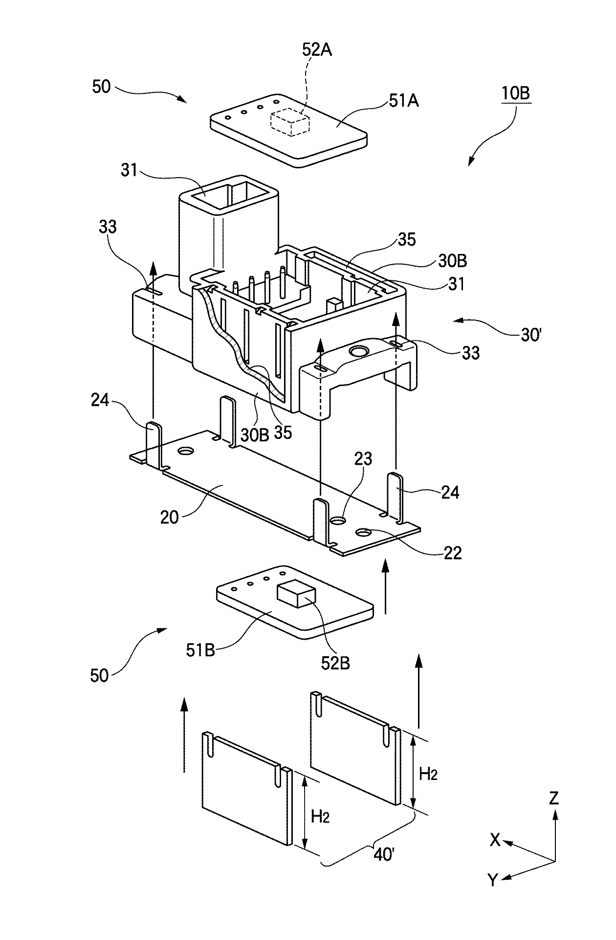
本実施形態の電流検出装置10Bは、第1の実施形態の電流検出装置10Aと異なり、バスバー20の上下位置に、センサ本体50の第1センサを構成する磁気検出素子52A及び第2センサを構成する磁気検出素子52Bが配置されている。また、本実施形態では、これらの磁気検出素子52A及び52Bをハウジング30´の上下に配置させるため、これらをそれぞれ実装した基板51A,51Bをハウジング30´の上下にそれぞれ取り付けてある。また、磁気シールド40´の大きさについても、第1の実施形態のものとは、高さ方向の寸法が若干異なる。
Unlike the current detection device 10 </ b> A of the first embodiment, the current detection device 10 </ b> B of the present embodiment configures the
ハウジング30´には、図6(B)に示すように、バスバー20の下面側に磁気検出素子52Bを実装する基板51Bが設置されるようにするため、上側のセンサ室32Aと同様のセンサ室32Bを形成してある。なお、磁気検出素子52Bは、基板51Bに対して上面に実装されている。
In the housing 30 ', as shown in FIG. 6B, a sensor chamber similar to the
磁気シールド40´については、図7に示すように、第1の実施形態の磁気シールド40と同様の一対の磁性板で構成されているが、上下の磁気検出素子52A,52Bが外部磁場から磁気遮蔽できるような高さ寸法H2を有する。
As shown in FIG. 7, the
即ち、磁気シールド40´は、外側の不要な磁界に対する、各磁気検出素子52A,52Bでの磁気遮蔽特性を同一にさせるため、各磁気検出素子52A,52Bに対し、バスバー20の高さ(Z)方向の中心位置Oからの遮蔽高さを同一になるように配置してある。つまり、バスバー20の中心位置Oから同一距離h1だけ離間した各磁気検出素子52A,52Bに対して、磁気シールド40´がそれぞれ同じ高さh2まで磁気遮蔽している。
That is, the
次に、本実施形態の電流検出のための磁気検出素子52A,52Bの作用について、特に図7乃至図9を参照しながら説明する。
本実施形態の電流検出装置10Bでは、図7に示すように、バスバー20に電流Iが流れると、第1の実施形態の場合と同様に、右ネジの法則に従ってそのバスバー20の周囲に、電流Iの流れに沿った右回りの磁力線を有する磁界が形成される。
Next, the operation of the
In the
即ち、本実施形態の電流検出装置10Bには、平板状の磁性板一対から構成された磁気シールド40´が、バスバー20の幅(Y)方向であるこの両側を囲設する状態で設置されている。このため、図7(A)に模式的に示すように、磁気シールド40´にも第1の実施形態のときと同様の磁路Mが形成される。
That is, in the
このように、各磁気シールド40´には、磁路Mが形成されるのと同時に、それぞれの磁気シールド40´の下端40´D及び上端40´Uには、第1の実施形態の場合と同様に、対応する端部どうしの間に例えば図7で示すような磁束Φが所定の分布パターンで形成される。なお、この図7では、典型的な磁束のパターンを記載してあるが、このパターンには限定されるものではない。
Thus, the magnetic path M is formed in each magnetic shield 40 ', and at the same time, the
特に、バスバー20の幅方向の中央部の直上で、かつ、各磁気シールド40´の上端40´Uよりも下方寄りに設置されている磁気検出素子52Aには、バスバー20の電流に伴い、その厚さ(Z)方向に対して直交する水平(−Y)方向に磁束Φが貫通する。従って、この磁気検出素子52Aには、バスバー20からの電流に伴う固有の分布パターンに生成された磁束密度Bが作用する。
In particular, the
即ち、磁気検出素子52Aを構成しているホール素子では、磁束密度Bの大きさに対応する強さのホール電場(即ち、電界の強さ)が生成され、この大きさに対応した出力電圧Vが得られる。そして、予め決定されているこの出力電圧Vとバスバー20の電流値iとの関係を示す適宜の関係式や対応表(テーブル)などから、バスバー20の電流値を検出できる。
That is, in the Hall element constituting the
一方、磁気検出素子52Bにもこれと同様の作用が生じる。つまり、バスバー20の幅方向の中央部の直下で、かつ、各磁気シールド40´の下端40´Dよりも上方寄りに設置されている磁気検出素子52Bには、その厚さ(Z)方向に対して直交する水平(−Y)方向に磁束Φが貫通する。従って、この磁気検出素子52Bには、バスバー20からの電流Iに伴う磁束密度Bが作用するので、磁束密度Bの大きさに対応する強さのホール電場(電界の強さE)が生成され、最終的に、この大きさに対応したバスバー20の電流値を検出できる。
On the other hand, the magnetic detecting
ところで、本実施形態では、磁気検出素子52A及び磁気検出素子52Bが、バスバー20に対して上下対称的に配置されている。従って、電流検出装置10Bに外部磁場が作用しない状況のときには、磁気検出素子52A及び磁気検出素子52Bで検出する電流値が、理論上同一値であることが予想される。しかしながら、これら双方の磁気検出素子52A及び磁気検出素子52Bにより検出する電流値が異なる場合には、何らかの外部磁場が作用していることが予想される。
By the way, in this embodiment, the
このような場合であっても、本実施形態の電流検出装置10Bによれば、図8に示す外部磁場Cの影響を除去した精度の高い電流値が検出できる。
即ち、同図に示すように、外部磁場が作用していない場合には、磁気検出素子52A及び52Bが、上下対称配置にある関係上、磁束密度Bの大きさは同じであって、貫通する磁束Φの方向のみが逆である。
Even in such a case, according to the
That is, as shown in the figure, when the external magnetic field is not acting, the
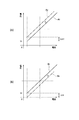
従って、磁気検出素子52A及び52Bに外部磁場Cが作用する場合には、その外部磁場Cに対応する分だけホール電場(即ち、電界の強さ)に変化、変動が出現する。つまり、図9(A)、(B)のように磁気検出素子52A及び磁気検出素子52Bに外部磁場が作用していないときに出力電圧のグラフA1、B1(実線部分)であるとする。一方、均一の外部磁場が作用すると、磁気検出素子52A及び磁気検出素子52Bからの出力電圧のグラフA2,B2(一点鎖線部分)に示すように、互いに反対方向にシフトする。その結果、外部磁場Cによる磁束密度Bの変化に比例した出力電圧Vの変化ΔVを受け、この変化ΔVを反映した出力電圧を出力する。
Therefore, when the external magnetic field C acts on the
但し、外部磁場Cが磁気検出素子52A及び52Bに均一に作用する場合には、磁気検出素子52A及び52Bからの出力電圧Vの変化は±ΔVとなって、符号のみが異なり絶対値が同一となる。従って、双方の出力電圧を加算するとキャンセルされる。即ち、
従って、この平均値を求めることで、バスバー20の電流値が算出可能となる。
However, when the external magnetic field C acts uniformly on the
Therefore, the current value of the
なお、各センサ、つまり磁気検出素子52A及び52Bの出力関係については、以下の[表1]を参照されたい。
For the output relationship of each sensor, that is, the
以上説明してきたように、本実施形態によれば、磁気検出素子が2つ必要となるが、この2つの磁気検出素子52A及び52Bをバスバー20の位置を基準として上下対称配置すれば、外部磁界を都合よくキャンセルできる。その結果、検出対象の電線やマグネット以外の外部磁場の存在する場所であっても、その影響を除去して精度の高い電流検出が可能となる。
As described above, according to the present embodiment, two magnetic detection elements are required. If these two
なお、本実施形態のような2つの磁気検出素子が対称配置された構成の場合であっても、磁気シールドが従来のような断面略コ字形のものを用いた場合には、外部磁界をキャンセルできないことに留意されたい。 Even in the case where the two magnetic detection elements are symmetrically arranged as in the present embodiment, the external magnetic field is canceled if the conventional magnetic shield has a substantially U-shaped cross section. Note that you can't.
また、本実施形態によれば、各磁気シールド40´である磁性板については、同一材料で形成した同一寸法を有するものを一対用意してバスバー20に対して対称配置させてあればよい。従って、従来のような形状、厚さ、材質などの検討が不要である。
Moreover, according to this embodiment, about the magnetic plate which is each magnetic shield 40 ', what has the same dimension formed with the same material should just prepare, and arrange | position with the
なお、本発明では、本実施形態を敷衍することにより、磁気シールドを設けていなくても、バスバーに対して上述のような対称配置の各磁気シールドを設置しておき、出力電圧に対して上述のような演算を行うことで、精度の高い電流検出が可能となる。その結果、基本的には、バスバーと2つの磁気検出素子があればよいので、磁気シールドが設置不要となる分、大幅な小型化、軽量化、コストの削減などが可能となる。 In the present invention, by laying out the present embodiment, each magnetic shield having the symmetrical arrangement as described above is installed on the bus bar even if no magnetic shield is provided, and the output voltage is described above. By performing such an operation, it is possible to detect current with high accuracy. As a result, basically, a bus bar and two magnetic detection elements are sufficient, so that a magnetic shield is not required to be installed, so that a significant reduction in size, weight, and cost can be achieved.
このように、本発明の電流検出装置では、磁気シールドが平板状のもの一対から構成されており、通常の断面略コ字形を有する磁気シールドのものに比して、実質的にその中央部を欠損させた構造である。従って、大型で大電流が流れる構造の幅広のバスバーに対してその電流検出を行うような構成とした場合には、幅広のバスバーに対応して幅広にさせる必要がない。つまり、狭い幅のバスバーにおける小電流検出の場合と同じ寸法の磁気シールドが使用可能となる。 As described above, in the current detection device of the present invention, the magnetic shield is composed of a pair of flat plate-like ones, and the center portion thereof is substantially compared with that of a magnetic shield having a generally U-shaped cross section. It is a deficient structure. Therefore, when the current detection is performed on a large bus bar having a structure in which a large current flows, it is not necessary to increase the width corresponding to the wide bus bar. In other words, a magnetic shield having the same dimensions as in the case of detecting a small current in a narrow bus bar can be used.
従って、本発明の電流検出装置によれば、薄板状の同一寸法の磁気遮蔽体を一対用いてこれを対称配置させた簡易な構成のもので、従来の断面略コ字形を有する磁気シールドを使用した電流検出装置に比べて、例えば凡そ2倍の±600Aまでの電流検出が可能となる。しかも、従来の断面略コ字形を有する磁気シールドでは、大電流検出の際に厚さを増大させる必要があるが、本発明ではその必要がなく、軽量なもので大電流検出が可能となる。 Therefore, according to the current detecting device of the present invention, a conventional magnetic shield having a substantially U-shaped cross section is used with a simple configuration in which a pair of thin magnetic shields having the same size are arranged symmetrically. Compared to the current detection device, for example, current detection up to ± 600 A, which is approximately twice as much, is possible. Moreover, in the conventional magnetic shield having a substantially U-shaped cross section, it is necessary to increase the thickness at the time of detecting a large current, but in the present invention, this is not necessary, and a large current can be detected with a light weight.
なお、本発明の電流検出装置は、これらの実施形態のような車両内のシステムの一部としての適用に限定されるものではなく、例えばバスバーなどを備えたものであれば、各種分野での電流検出装置としての適用が可能である。 Note that the current detection device of the present invention is not limited to application as a part of a system in a vehicle as in these embodiments. For example, as long as it includes a bus bar or the like, it can be used in various fields. Application as a current detection device is possible.
10A,10A1,10A2,10B 電流検出装置
20 バスバー(導電体)
23 ネジ挿入孔
24 起立片
30 ハウジング
30B 第2側面
31 コネクタ室
32、32A、32B センサ室
35 細溝孔
40、40´ 磁気シールド(磁気遮蔽体)
40D (磁気シールドの)下端
40M 磁性体
40U、40´U (磁気シールドの)上端
50 センサ本体
51 基板
52 磁気検出素子
52A 第1センサ(磁気検出素子)
52B 第2センサ(磁気検出素子)
A1 第1センサに外部磁場が作用していないときのグラフ
A2 第1センサに外部磁場が作用したときのグラフ
B 磁束密度(磁気誘導)
B1 第2センサに外部磁場が作用していないときのグラフ
B2 第2センサに外部磁場が作用したときのグラフ
H 磁界の強さ
H1,H2 磁気シールド(磁気遮蔽体)の高さ
h1 バスバー(導電体)からセンサまでの高さ
M 磁路
S 合成樹脂のネジ
α コネクタ連結部
β 検出部
Φ 磁束
10A, 10A 1 , 10A 2 , 10B
23
40D Lower end of
52B Second sensor (magnetic detection element)
A 1 Graph when an external magnetic field is not acting on the first sensor A 2 Graph when an external magnetic field is acting on the first sensor B Magnetic flux density (magnetic induction)
B 1 Graph when an external magnetic field is not applied to the second sensor B 2 Graph when an external magnetic field is applied to the second sensor H Magnetic field strengths H 1 and H 2 Magnetic shield (magnetic shield) height h1 Height from the bus bar (conductor) to the sensor M Magnetic path S Synthetic resin screw α Connector connection part β Detection part Φ Magnetic flux
Claims (3)
前記磁気検出素子は、前記導電体の近傍の、導電体の幅方向の中央部に臨んで設置されているとともに、
前記磁気遮蔽体は、同一寸法を有する一対のものが、前記導電体の幅方向の両側縁を外側から挟むような状態で、導電体に対して対称に対向配置されている、
ことを特徴とする電流検出装置。 A magnetic detection element for detecting a magnetic flux density or a magnetic field intensity formed by a current value flowing through the conductor is provided in a region magnetically shielded by the magnetic shield, and the current value flowing through the conductor is detected by the magnetic detection. A current detection device for detecting with an element,
The magnetic detection element is installed facing the central portion in the width direction of the conductor in the vicinity of the conductor,
The pair of magnetic shields having the same dimensions are disposed symmetrically opposite the conductor in a state where both side edges in the width direction of the conductor are sandwiched from outside.
A current detection device characterized by that.
周囲が壁面で囲設されてセンサを収容するセンサ室を有し、前記バスバーの一方の面に底面が臨む、非磁性体で形成されたハウジングをさらに備え、
前記磁気遮蔽体は、前記ハウジングのセンサ室の互いに対向する両壁面に、前記バスバーの幅方向の両側縁を外側から挟むような状態で対称的に設けた同一形状を有する一対の磁性板で構成され、
前記センサ室内の前記バスバー幅方向の横断面における磁界は、前記磁気検出素子を中心として対称的な分布パターンで生成される、
ことを特徴とする請求項1に記載の電流検出装置。 The conductor is a wide plate bus bar,
A housing formed of a non-magnetic material, having a sensor chamber that is surrounded by a wall surface and accommodates a sensor, with a bottom surface facing one surface of the bus bar;
The magnetic shield is composed of a pair of magnetic plates having the same shape symmetrically provided on both opposing wall surfaces of the sensor chamber of the housing in such a manner that both side edges of the bus bar are sandwiched from the outside. And
The magnetic field in the cross section in the bus bar width direction in the sensor chamber is generated in a symmetrical distribution pattern with the magnetic detection element as the center.
The current detection device according to claim 1.
前記第1センサ及び前記第2センサは、前記バスバーの厚さ方向の中心位置を基準として上下対称的に配置されている、
ことを特徴とする請求項1又は2に記載の電流検出装置。 The magnetic detection element includes a first sensor disposed in a central portion in the width direction in the vicinity of one surface of the bus bar in the sensor chamber, and a central portion in the width direction in the vicinity of the other surface of the bus bar. A second sensor disposed in the
The first sensor and the second sensor are arranged symmetrically with respect to the center position in the thickness direction of the bus bar.
The current detection device according to claim 1, wherein:
Priority Applications (1)
| Application Number | Priority Date | Filing Date | Title |
|---|---|---|---|
| JP2011258040A JP2013113631A (en) | 2011-11-25 | 2011-11-25 | Current detector |
Applications Claiming Priority (1)
| Application Number | Priority Date | Filing Date | Title |
|---|---|---|---|
| JP2011258040A JP2013113631A (en) | 2011-11-25 | 2011-11-25 | Current detector |
Publications (1)
| Publication Number | Publication Date |
|---|---|
| JP2013113631A true JP2013113631A (en) | 2013-06-10 |
Family
ID=48709308
Family Applications (1)
| Application Number | Title | Priority Date | Filing Date |
|---|---|---|---|
| JP2011258040A Pending JP2013113631A (en) | 2011-11-25 | 2011-11-25 | Current detector |
Country Status (1)
| Country | Link |
|---|---|
| JP (1) | JP2013113631A (en) |
Cited By (5)
| Publication number | Priority date | Publication date | Assignee | Title |
|---|---|---|---|---|
| JP2016206015A (en) * | 2015-04-23 | 2016-12-08 | カルソニックカンセイ株式会社 | Bus bar assembled current sensor |
| US9915685B2 (en) | 2014-01-23 | 2018-03-13 | Denso Corporation | Electrical current detection system |
| WO2019117174A1 (en) * | 2017-12-13 | 2019-06-20 | アルプスアルパイン株式会社 | Current sensor |
| CN109962629A (en) * | 2017-12-22 | 2019-07-02 | 维洛西门子新能源汽车法国简式股份公司 | Electrical equipment and its casing member |
| WO2022181063A1 (en) * | 2021-02-24 | 2022-09-01 | サンコール株式会社 | Current sensor |
-
2011
- 2011-11-25 JP JP2011258040A patent/JP2013113631A/en active Pending
Cited By (8)
| Publication number | Priority date | Publication date | Assignee | Title |
|---|---|---|---|---|
| US9915685B2 (en) | 2014-01-23 | 2018-03-13 | Denso Corporation | Electrical current detection system |
| JP2016206015A (en) * | 2015-04-23 | 2016-12-08 | カルソニックカンセイ株式会社 | Bus bar assembled current sensor |
| WO2019117174A1 (en) * | 2017-12-13 | 2019-06-20 | アルプスアルパイン株式会社 | Current sensor |
| JPWO2019117174A1 (en) * | 2017-12-13 | 2020-10-01 | アルプスアルパイン株式会社 | Current sensor |
| US11287451B2 (en) | 2017-12-13 | 2022-03-29 | Alps Alpine Co., Ltd. | Current sensor |
| CN109962629A (en) * | 2017-12-22 | 2019-07-02 | 维洛西门子新能源汽车法国简式股份公司 | Electrical equipment and its casing member |
| WO2022181063A1 (en) * | 2021-02-24 | 2022-09-01 | サンコール株式会社 | Current sensor |
| EP4270018A4 (en) * | 2021-02-24 | 2024-07-03 | Suncall Corp | Current sensor |
Similar Documents
| Publication | Publication Date | Title |
|---|---|---|
| JP4835868B2 (en) | Current sensor | |
| JP5464098B2 (en) | Current detector | |
| US11105831B2 (en) | Current sensor | |
| JP5659389B2 (en) | Current sensor | |
| CN108450013B (en) | Current sensor and power conversion device provided with same | |
| US11041887B2 (en) | Current sensor | |
| WO2016194240A1 (en) | Electric current sensor | |
| JP2015049184A (en) | Inverter device | |
| JP2010008050A (en) | Current sensor | |
| JPWO2006090769A1 (en) | Current measuring device | |
| JP2012068154A (en) | Current detector and attachment structure thereof | |
| JP2013113631A (en) | Current detector | |
| JP2005321206A (en) | Current detection device | |
| WO2012046547A1 (en) | Current sensor | |
| JP2022519060A (en) | Current transducer with magnetic field detector module | |
| JP6032534B2 (en) | Magnetic shield and current detector provided with the same | |
| JP5225884B2 (en) | Assembling structure and assembling method of current detection device | |
| JP2007155399A (en) | Current sensor and current value calculation system having the same | |
| WO2016047292A1 (en) | Electric current sensor | |
| JP5960403B2 (en) | Current sensor | |
| JP2012063285A (en) | Current sensor | |
| JP5704352B2 (en) | Current sensor | |
| CN214539763U (en) | Current detection device | |
| JP2012141262A (en) | Current detection device | |
| EP4043890A1 (en) | Magnetic sensor and current detection device comprising same |