JP2012513672A - Electronic circuit board manufacturing method using electrophotography - Google Patents
Electronic circuit board manufacturing method using electrophotography Download PDFInfo
- Publication number
- JP2012513672A JP2012513672A JP2011542124A JP2011542124A JP2012513672A JP 2012513672 A JP2012513672 A JP 2012513672A JP 2011542124 A JP2011542124 A JP 2011542124A JP 2011542124 A JP2011542124 A JP 2011542124A JP 2012513672 A JP2012513672 A JP 2012513672A
- Authority
- JP
- Japan
- Prior art keywords
- conductive powder
- substrate
- image
- thermoplastic
- particles
- Prior art date
- Legal status (The legal status is an assumption and is not a legal conclusion. Google has not performed a legal analysis and makes no representation as to the accuracy of the status listed.)
- Withdrawn
Links
Images


Classifications
-
- H—ELECTRICITY
- H05—ELECTRIC TECHNIQUES NOT OTHERWISE PROVIDED FOR
- H05K—PRINTED CIRCUITS; CASINGS OR CONSTRUCTIONAL DETAILS OF ELECTRIC APPARATUS; MANUFACTURE OF ASSEMBLAGES OF ELECTRICAL COMPONENTS
- H05K3/00—Apparatus or processes for manufacturing printed circuits
- H05K3/10—Apparatus or processes for manufacturing printed circuits in which conductive material is applied to the insulating support in such a manner as to form the desired conductive pattern
- H05K3/12—Apparatus or processes for manufacturing printed circuits in which conductive material is applied to the insulating support in such a manner as to form the desired conductive pattern using thick film techniques, e.g. printing techniques to apply the conductive material or similar techniques for applying conductive paste or ink patterns
- H05K3/1266—Apparatus or processes for manufacturing printed circuits in which conductive material is applied to the insulating support in such a manner as to form the desired conductive pattern using thick film techniques, e.g. printing techniques to apply the conductive material or similar techniques for applying conductive paste or ink patterns by electrographic or magnetographic printing
-
- B—PERFORMING OPERATIONS; TRANSPORTING
- B65—CONVEYING; PACKING; STORING; HANDLING THIN OR FILAMENTARY MATERIAL
- B65H—HANDLING THIN OR FILAMENTARY MATERIAL, e.g. SHEETS, WEBS, CABLES
- B65H85/00—Recirculating articles, i.e. feeding each article to, and delivering it from, the same machine work-station more than once
-
- G—PHYSICS
- G03—PHOTOGRAPHY; CINEMATOGRAPHY; ANALOGOUS TECHNIQUES USING WAVES OTHER THAN OPTICAL WAVES; ELECTROGRAPHY; HOLOGRAPHY
- G03G—ELECTROGRAPHY; ELECTROPHOTOGRAPHY; MAGNETOGRAPHY
- G03G15/00—Apparatus for electrographic processes using a charge pattern
- G03G15/14—Apparatus for electrographic processes using a charge pattern for transferring a pattern to a second base
- G03G15/16—Apparatus for electrographic processes using a charge pattern for transferring a pattern to a second base of a toner pattern, e.g. a powder pattern, e.g. magnetic transfer
- G03G15/1625—Apparatus for electrographic processes using a charge pattern for transferring a pattern to a second base of a toner pattern, e.g. a powder pattern, e.g. magnetic transfer on a base other than paper
-
- G—PHYSICS
- G03—PHOTOGRAPHY; CINEMATOGRAPHY; ANALOGOUS TECHNIQUES USING WAVES OTHER THAN OPTICAL WAVES; ELECTROGRAPHY; HOLOGRAPHY
- G03G—ELECTROGRAPHY; ELECTROPHOTOGRAPHY; MAGNETOGRAPHY
- G03G15/00—Apparatus for electrographic processes using a charge pattern
- G03G15/22—Apparatus for electrographic processes using a charge pattern involving the combination of more than one step according to groups G03G13/02 - G03G13/20
- G03G15/221—Machines other than electrographic copiers, e.g. electrophotographic cameras, electrostatic typewriters
- G03G15/224—Machines for forming tactile or three dimensional images by electrographic means, e.g. braille, 3d printing
-
- G—PHYSICS
- G03—PHOTOGRAPHY; CINEMATOGRAPHY; ANALOGOUS TECHNIQUES USING WAVES OTHER THAN OPTICAL WAVES; ELECTROGRAPHY; HOLOGRAPHY
- G03G—ELECTROGRAPHY; ELECTROPHOTOGRAPHY; MAGNETOGRAPHY
- G03G15/00—Apparatus for electrographic processes using a charge pattern
- G03G15/65—Apparatus which relate to the handling of copy material
- G03G15/6582—Special processing for irreversibly adding or changing the sheet copy material characteristics or its appearance, e.g. stamping, annotation printing, punching
- G03G15/6585—Special processing for irreversibly adding or changing the sheet copy material characteristics or its appearance, e.g. stamping, annotation printing, punching by using non-standard toners, e.g. transparent toner, gloss adding devices
-
- G—PHYSICS
- G03—PHOTOGRAPHY; CINEMATOGRAPHY; ANALOGOUS TECHNIQUES USING WAVES OTHER THAN OPTICAL WAVES; ELECTROGRAPHY; HOLOGRAPHY
- G03G—ELECTROGRAPHY; ELECTROPHOTOGRAPHY; MAGNETOGRAPHY
- G03G15/00—Apparatus for electrographic processes using a charge pattern
- G03G15/65—Apparatus which relate to the handling of copy material
- G03G15/6588—Apparatus which relate to the handling of copy material characterised by the copy material, e.g. postcards, large copies, multi-layered materials, coloured sheet material
- G03G15/6591—Apparatus which relate to the handling of copy material characterised by the copy material, e.g. postcards, large copies, multi-layered materials, coloured sheet material characterised by the recording material, e.g. plastic material, OHP, ceramics, tiles, textiles
-
- B—PERFORMING OPERATIONS; TRANSPORTING
- B65—CONVEYING; PACKING; STORING; HANDLING THIN OR FILAMENTARY MATERIAL
- B65H—HANDLING THIN OR FILAMENTARY MATERIAL, e.g. SHEETS, WEBS, CABLES
- B65H2301/00—Handling processes for sheets or webs
- B65H2301/30—Orientation, displacement, position of the handled material
- B65H2301/33—Modifying, selecting, changing orientation
- B65H2301/333—Inverting
- B65H2301/3331—Involving forward reverse transporting means
- B65H2301/33312—Involving forward reverse transporting means forward reverse rollers pairs
-
- G—PHYSICS
- G03—PHOTOGRAPHY; CINEMATOGRAPHY; ANALOGOUS TECHNIQUES USING WAVES OTHER THAN OPTICAL WAVES; ELECTROGRAPHY; HOLOGRAPHY
- G03G—ELECTROGRAPHY; ELECTROPHOTOGRAPHY; MAGNETOGRAPHY
- G03G2215/00—Apparatus for electrophotographic processes
- G03G2215/00362—Apparatus for electrophotographic processes relating to the copy medium handling
- G03G2215/00443—Copy medium
- G03G2215/00523—Other special types, e.g. tabbed
-
- H—ELECTRICITY
- H05—ELECTRIC TECHNIQUES NOT OTHERWISE PROVIDED FOR
- H05K—PRINTED CIRCUITS; CASINGS OR CONSTRUCTIONAL DETAILS OF ELECTRIC APPARATUS; MANUFACTURE OF ASSEMBLAGES OF ELECTRICAL COMPONENTS
- H05K2201/00—Indexing scheme relating to printed circuits covered by H05K1/00
- H05K2201/01—Dielectrics
- H05K2201/0104—Properties and characteristics in general
- H05K2201/0129—Thermoplastic polymer, e.g. auto-adhesive layer; Shaping of thermoplastic polymer
-
- H—ELECTRICITY
- H05—ELECTRIC TECHNIQUES NOT OTHERWISE PROVIDED FOR
- H05K—PRINTED CIRCUITS; CASINGS OR CONSTRUCTIONAL DETAILS OF ELECTRIC APPARATUS; MANUFACTURE OF ASSEMBLAGES OF ELECTRICAL COMPONENTS
- H05K2201/00—Indexing scheme relating to printed circuits covered by H05K1/00
- H05K2201/02—Fillers; Particles; Fibers; Reinforcement materials
- H05K2201/0203—Fillers and particles
- H05K2201/0206—Materials
- H05K2201/0224—Conductive particles having an insulating coating
-
- H—ELECTRICITY
- H05—ELECTRIC TECHNIQUES NOT OTHERWISE PROVIDED FOR
- H05K—PRINTED CIRCUITS; CASINGS OR CONSTRUCTIONAL DETAILS OF ELECTRIC APPARATUS; MANUFACTURE OF ASSEMBLAGES OF ELECTRICAL COMPONENTS
- H05K2203/00—Indexing scheme relating to apparatus or processes for manufacturing printed circuits covered by H05K3/00
- H05K2203/05—Patterning and lithography; Masks; Details of resist
- H05K2203/0502—Patterning and lithography
- H05K2203/0517—Electrographic patterning
-
- H—ELECTRICITY
- H05—ELECTRIC TECHNIQUES NOT OTHERWISE PROVIDED FOR
- H05K—PRINTED CIRCUITS; CASINGS OR CONSTRUCTIONAL DETAILS OF ELECTRIC APPARATUS; MANUFACTURE OF ASSEMBLAGES OF ELECTRICAL COMPONENTS
- H05K2203/00—Indexing scheme relating to apparatus or processes for manufacturing printed circuits covered by H05K3/00
- H05K2203/05—Patterning and lithography; Masks; Details of resist
- H05K2203/0502—Patterning and lithography
- H05K2203/0522—Using an adhesive pattern
-
- H—ELECTRICITY
- H05—ELECTRIC TECHNIQUES NOT OTHERWISE PROVIDED FOR
- H05K—PRINTED CIRCUITS; CASINGS OR CONSTRUCTIONAL DETAILS OF ELECTRIC APPARATUS; MANUFACTURE OF ASSEMBLAGES OF ELECTRICAL COMPONENTS
- H05K2203/00—Indexing scheme relating to apparatus or processes for manufacturing printed circuits covered by H05K3/00
- H05K2203/07—Treatments involving liquids, e.g. plating, rinsing
- H05K2203/0779—Treatments involving liquids, e.g. plating, rinsing characterised by the specific liquids involved
- H05K2203/0783—Using solvent, e.g. for cleaning; Regulating solvent content of pastes or coatings for adjusting the viscosity
-
- H—ELECTRICITY
- H05—ELECTRIC TECHNIQUES NOT OTHERWISE PROVIDED FOR
- H05K—PRINTED CIRCUITS; CASINGS OR CONSTRUCTIONAL DETAILS OF ELECTRIC APPARATUS; MANUFACTURE OF ASSEMBLAGES OF ELECTRICAL COMPONENTS
- H05K2203/00—Indexing scheme relating to apparatus or processes for manufacturing printed circuits covered by H05K3/00
- H05K2203/15—Position of the PCB during processing
- H05K2203/1572—Processing both sides of a PCB by the same process; Providing a similar arrangement of components on both sides; Making interlayer connections from two sides
Landscapes
- Physics & Mathematics (AREA)
- General Physics & Mathematics (AREA)
- Engineering & Computer Science (AREA)
- Manufacturing & Machinery (AREA)
- Ceramic Engineering (AREA)
- Textile Engineering (AREA)
- Microelectronics & Electronic Packaging (AREA)
- Manufacturing Of Printed Wiring (AREA)
- Combination Of More Than One Step In Electrophotography (AREA)
Abstract
プリント配線を製造する方法であり:かかる方法は、プライマリイメージ部材を荷電し;基板上に熱可塑性物質を含むパターンをイメージに基づき生成し;前記基板上に導電性粉末を堆積させ;前記導電性粉末を前記熱可塑性基板上に恒久的に固定し;前記熱可塑性パターンでコーティングされた以外の基板の部分から前記導電性粉末を除去するステップを含む。
A method of manufacturing a printed wiring: charging a primary image member; generating a pattern comprising a thermoplastic material on a substrate based on an image; depositing conductive powder on the substrate; Permanently fixing powder on the thermoplastic substrate; removing the conductive powder from portions of the substrate other than coated with the thermoplastic pattern.
Description
本発明は、プリント電子回路、より具体的には電子写真を用いる電子回路基板の製造方法に関する。 The present invention relates to a method of manufacturing a printed electronic circuit, more specifically an electronic circuit board using electrophotography.
プリント回路基板は、非導電性基板上にラミネートされた銅シートからエッチングされた導電性パス又はトレースを用いて電子コンポーネントを機械的に保持しかつ電気的に結合するために用いられている。プリント回路基板はまた、プリントワイヤボード又はエッチングワイヤボードとしても参照される。電子コンポーネントが集積されたプリント回路はプリント回路アセンブリ又はプリント回路基板アセンブリとして知られている。 Printed circuit boards are used to mechanically hold and electrically bond electronic components using conductive paths or traces etched from a copper sheet laminated on a non-conductive substrate. Printed circuit boards are also referred to as printed wire boards or etched wire boards. Printed circuits with integrated electronic components are known as printed circuit assemblies or printed circuit board assemblies.
プリント回路は、丈夫、安価でありかつ高い信頼性を有する。プリント回路は、ワイヤラッピング回路や空中配線回路に比べるとずっと多くレイアウトへの努力と高い初期費用が必要であるが、大量生産するにはずっと安価であり迅速である。導電層は通常薄い銅ホイルからなる。絶縁層は通常エポキシ樹脂と共にラミネートされている。基板は通常緑色とされ、例えばポリテトラフルオロエチレン、FR−4、FR−1,CEMー1又はCEM−3からなる。PCB工業で使用されるよく知られたプレプレグ材料は、FR−2(フェノールコットンペーパ)、FR−3(コットンペーパとエポキシ),FR−4(織ガラスとエポキシ),FR−5(織ガラスとエポキシ),FR−6(マットガラスとポリエステル),G−10(織ガラスとエポキシ),CEM−I(コットンペーパとエポキシ),CEM−2(コットンペーパとエポキシ),CEM−3(織ガラスとエポキシ),CEM−4(織ガラスとエポキシ),CEM−5(織ガラスとポリエステル)が挙げられる。 Printed circuits are robust, inexpensive and highly reliable. Printed circuits require much more layout effort and higher initial costs than wire wrapping and aerial wiring circuits, but are much cheaper and faster for mass production. The conductive layer usually consists of a thin copper foil. The insulating layer is usually laminated with an epoxy resin. The substrate is usually green, and is made of, for example, polytetrafluoroethylene, FR-4, FR-1, CEM-1, or CEM-3. Well known prepreg materials used in the PCB industry are: FR-2 (phenolic cotton paper), FR-3 (cotton paper and epoxy), FR-4 (woven glass and epoxy), FR-5 (with woven glass) Epoxy), FR-6 (matte glass and polyester), G-10 (woven glass and epoxy), CEM-I (cotton paper and epoxy), CEM-2 (cotton paper and epoxy), CEM-3 (with woven glass) Epoxy), CEM-4 (woven glass and epoxy), and CEM-5 (woven glass and polyester).
ほとんどのプリント配線基板は、基板全体上、ある場合には両面に銅の層を結合することで作られ(「ブランクPCB」の製造)、その後一時的マスクを適用して不要な銅を除去し(例えばエッチングによる)、望ましい銅トレースのみを残す。あるPCBは、基板自体(又は非常に薄い銅層を有する基板)に、通常複数のメッキを用いる複雑な工程によりトレースを加えて製造されている。 Most printed wiring boards are made by bonding a layer of copper on the entire board, in some cases on both sides (“blank PCB” manufacturing), and then applying a temporary mask to remove unwanted copper. Leave only the desired copper trace (eg by etching). Some PCBs are manufactured by adding traces to the substrate itself (or a substrate with a very thin copper layer) by a complex process that typically uses multiple platings.
これまで3種類の「サブトラクト」方法(銅を除去する方法)が、プリント配線基板を製造するために使用されている。 So far, three types of “subtract” methods (methods for removing copper) have been used to produce printed wiring boards.
シルクスクリーン印刷方法は、銅ホイルを保護するためにエッチング耐性インクを用いる。続くエッチングにより不要な銅が除去される。または該インクが導電性であり、ブランク基板(非導電性)上に印刷されてもよい。かかる技術はまた、ハイブリッド配線を製造する際に使用される。 The silk screen printing method uses an etch resistant ink to protect the copper foil. Subsequent etching removes unwanted copper. Alternatively, the ink may be conductive and printed on a blank substrate (non-conductive). Such techniques are also used in manufacturing hybrid wiring.
光彫刻方法は、ホトマスクと化学エッチングを用いて基板から銅を除去する。かかるホトマスクは通常CAMを用いる技術者やコンピュータ補助製造ソフトウエアにより生成されるデータから光プロッタを用いて製造される。レーザープリント透明物が通常、ホトツールとして適用されるが、直接のレーザーイメージ技術が高分解の要求のためにホトツールに代えて提供される。 The photoengraving method removes copper from the substrate using a photomask and chemical etching. Such a photomask is usually manufactured using an optical plotter from data generated by an engineer using CAM or computer-aided manufacturing software. Laser printed transparency is usually applied as a phototool, but direct laser image technology is provided in place of the phototool for high resolution requirements.
PCBミリングは、2又は3軸の機械的ミリングシステムを用いて基板から銅ホイルを取り除く。PCBミリング装置(PCBプロトタイパと参照される)は、プロッタと同様の方法で操作される。即ち、ミリングヘッドのx、y及び(適切ならば)z軸での位置を制御するソフトウエアからの命令を受ける。プロトタイパを駆動するデータは、PCBデザインソフトウエアで生成されHPGL又はGerberファイルフォーマットで保存されたファイルから取り出される。 PCB milling uses a 2- or 3-axis mechanical milling system to remove the copper foil from the substrate. A PCB milling device (referred to as a PCB prototyper) is operated in the same way as a plotter. That is, it receives commands from software that controls the milling head's x, y and (if appropriate) z-axis position. The data that drives the prototyper is retrieved from a file generated by the PCB design software and saved in the HPGL or Gerber file format.
「追加」プロセスがまた存在する。もっとも普通は、「準追加プロセス」である。これによると、パターン化されていない基板はその上に薄い銅層を予め有する。リバースマスクをそこに適用する(サブトラクトプロセスとは異なり、このマスクは最終的にはトレースとして残る基板上のかかる部分を露光する)。マスクがされていない基板上に追加の銅をメッキする。メッキされる銅は望ましい厚さにすることができる。更にその後スズー鉛又は他の表面メッキを行う。マスクを剥がし、短いエッチングをして基板上に現れた最初の銅ラミネートを基板から除去し、個々のトレースを切り離す。 There is also an “add” process. The most common is the “semi-addition process”. According to this, the unpatterned substrate already has a thin copper layer on it. A reverse mask is applied there (unlike a subtract process, this mask eventually exposes that part of the substrate that remains as a trace). Plating additional copper on the unmasked substrate. The copper to be plated can be of a desired thickness. Further tin-lead or other surface plating is then performed. The mask is stripped and a short etch is performed to remove the first copper laminate appearing on the substrate from the substrate and separate individual traces.
追加プロセスは通常マルチレイヤ基板の製造に使用され、基板内のホール(導電性バイアスを作るための)をメッキして通じるようにする。 An additional process is typically used in the manufacture of multi-layer substrates, where holes in the substrate (to create a conductive bias) are plated through.
レシーバ部材上にイメージを印刷するひとつの方法は、電子写真に関する。この方法では、均一に荷電された絶縁体部材上に静電気イメージを形成し、前記均一に荷電された領域を選択的に放電させてイメージに基づく静電気パターンを生成する。かかる放電は通常均一に荷電された絶縁部材に、かかる絶縁部材に向けられたLEDアレイ又はレーザー装置の選択的に活性化された特定の光源による紫外線を放射することで達成される。前記イメージに基づく荷電パターンが形成された後、顔料(又はある場合、非顔料)マーキング粒子が実質的に前記絶縁材料上の荷電パターンと逆の電荷を付与されて前記絶縁材料の近くに配置され、前記イメージに基づく荷電パターンに引き寄せられて可視イメージへとそのパターンを現像させる。 One method for printing an image on a receiver member relates to electrophotography. In this method, an electrostatic image is formed on a uniformly charged insulator member, and the uniformly charged region is selectively discharged to generate an electrostatic pattern based on the image. Such discharge is usually accomplished by irradiating a uniformly charged insulating member with ultraviolet light from a specific activated light source of an LED array or laser device directed to such insulating member. After the image-based charged pattern is formed, pigment (or non-pigmented in some cases) marking particles are placed near the insulating material with a charge substantially opposite to the charged pattern on the insulating material. , Attracted to the charged pattern based on the image to develop the pattern into a visible image.
その後、適切なレシーバ部材(例えば、平面ボンド紙)を、前記絶縁材料上の現像されたイメージに基づく前記マーキング粒子と並置させる。適切な電場を与えて前記マーキング粒子を前記レシーバ部材上に前記イメージに基づくパターンに移して前記レシーバ部材上に前記望ましいプリントイメージを形成する。前記レシーバ部材はその後、前記絶縁材料に伴う操作から取り出され、前記マーキング粒子は通常熱及び/又は圧力と熱を用いて前記レシーバ部材上に恒久的に固定される。複数層又はマーキング材料は、ひとつのレシーバ部材に重ねられてもよい。例えば異なる色の粒子の層がひとつのレシーバ部材上に重なられ、固定化後複数色のプリントイメージを前記レシーバ部材上に形成することができる。 Thereafter, a suitable receiver member (eg, planar bond paper) is juxtaposed with the marking particles based on the developed image on the insulating material. An appropriate electric field is applied to transfer the marking particles to the image-based pattern on the receiver member to form the desired print image on the receiver member. The receiver member is then removed from the operation associated with the insulating material, and the marking particles are permanently fixed on the receiver member using normal heat and / or pressure and heat. Multiple layers or marking materials may be superimposed on a single receiver member. For example, layers of different colored particles can be overlaid on a single receiver member, and a multi-color print image can be formed on the receiver member after immobilization.
商業上の印刷において、金属コーティング印刷物および電子配線の製造において、例えばアルミニウムや金である金属フィルムが使用される。最近、種々の材料上に、広範な種類の反射及び電気的導電性の薄いフィルムを含む金属フィルムをスタンプする装置が市販されている。 In commercial printing, metal films, such as aluminum or gold, are used in the production of printed metal coatings and electronic wiring. Recently, devices for stamping metal films including a wide variety of reflective and electrically conductive thin films on various materials are commercially available.
パターン化導電性構造を製造する技術分野において、短期での費用効果の点又は種々の情報を持つという点で、強い要求がある。優れた電極性能を提供することに加えて、これらの導電層はまた、デジタル的パターン化される必要があり、湿度の変化の影響を受けずかつ合理的な費用で製造可能なものでなければならない。 There is a strong demand in the technical field of manufacturing patterned conductive structures in terms of short-term cost effectiveness or having various information. In addition to providing superior electrode performance, these conductive layers also need to be digitally patterned, must be unaffected by changes in humidity and can be manufactured at a reasonable cost. Don't be.
本発明の課題は、かかる導電性が改良されかつデジタル的にパターン化された物であって、従来技術よりもより広範な商業上の要求を満たす物を提供することである。 It is an object of the present invention to provide such an improved conductivity and digitally patterned product that meets a wider range of commercial requirements than the prior art.
本発明のプリント配線は、電子写真プロセスを用いるひとつ又はそれ以上のトナーの適用によりパターン化される。最終のパターンは圧力及び(又は)熱固定ステップにより「固定」される。即ち前記トナー粒子が導電粒子と相互作用して前記導電性粒子を基板に接着する。 The printed wiring of the present invention is patterned by applying one or more toners using an electrophotographic process. The final pattern is “fixed” by pressure and / or heat setting steps. That is, the toner particles interact with the conductive particles to adhere the conductive particles to the substrate.
本発明は、電子写真を用いて基板上に配線をプリントする方法を提供する。 The present invention provides a method for printing wiring on a substrate using electrophotography.
本発明のひとつの実施態様は、プリント配線を製造する方法に関し、かかる方法は、
基板上に熱可塑性物質を含むパターンをイメージに基づき生成し、
前記基板上に導電性粉末を堆積させ、
前記導電性粉末を前記熱可塑性基板上に恒久的に固定し、
前記熱可塑性パターンでコーティングされた以外の基板の部分から前記導電性粉末を除去する、ステップを含む。
One embodiment of the present invention relates to a method of manufacturing a printed wiring, such a method comprising:
Generate a pattern containing thermoplastic material on the substrate based on the image,
Depositing conductive powder on the substrate;
Permanently fixing the conductive powder on the thermoplastic substrate;
Removing the conductive powder from portions of the substrate other than those coated with the thermoplastic pattern.
本発明の他の実施態様は、プリント配線を製造する方法に関し、かかる方法は、
プライマリイメージ部材を荷電し、
前記プライマリイメージ部材にイメージに基づく暴露により静電的潜在イメージを生成し、
前記プライマリイメージ部材上に熱可塑性粒子をイメージに基づき堆積し、
前記熱可塑性粒子を、電気的絶縁基板に移し、
前記基板上に導電性粉末を堆積し、
前記導電性粉末を前記基板上に恒久的に固定し、及び
前記熱可塑性パターンでコーティングされていない他の基板の部分から前記導電性粉末を除去する、ステップを含む。
Another embodiment of the invention relates to a method of manufacturing a printed wiring, such a method comprising:
Charge the primary image member,
Generating an electrostatic latent image by image-based exposure to the primary image member;
Depositing thermoplastic particles on the primary image member based on the image;
Transferring the thermoplastic particles to an electrically insulating substrate;
Depositing conductive powder on the substrate;
Permanently fixing the conductive powder onto the substrate and removing the conductive powder from portions of the other substrate not coated with the thermoplastic pattern.
本発明のさらなる実施態様は、プリント配線の製造方法であり、かかる方法は、
プライマリイメージ部材を荷電し、
前記プライマリイメージ部材にイメージに基づく暴露により静電的潜在イメージを生成し、
前記プライマリイメージ部材上に熱可塑性粒子をイメージに基づき堆積し、
前記熱可塑性粒子を、電気的絶縁基板に移し、
前記導電性粉末を前記基板上に恒久的に固定し、
前記基板上に導電性粉末を堆積し、
前記導電性粉末を前記基板上に恒久的に固定し、
前記熱可塑性パターンでコーティングされていない他の基板の部分から前記導電性粉末を除去し、及び
前記導電性粒子を、熱及び/又は圧力により前記熱可塑性物質中に入れ込む、
ステップを含む。
A further embodiment of the present invention is a method of manufacturing a printed wiring, such a method comprising:
Charge the primary image member,
Generating an electrostatic latent image by image-based exposure to the primary image member;
Depositing thermoplastic particles on the primary image member based on the image;
Transferring the thermoplastic particles to an electrically insulating substrate;
Permanently fixing the conductive powder on the substrate;
Depositing conductive powder on the substrate;
Permanently fixing the conductive powder on the substrate;
Removing the conductive powder from the portion of the other substrate not coated with the thermoplastic pattern, and entraining the conductive particles into the thermoplastic by heat and / or pressure;
Includes steps.
本発明の他の実施態様は、多層のプリント配線の製造方法であり、かかる方法は、
プライマリイメージ部材に荷電し、
前記イメージをイメージに基づき暴露して静電潜在イメージを生成し、
前記プライマリイメージ部材上に熱可塑性粒子をイメージの基づき堆積させ、
前記熱可塑性粒子を電気的に絶縁部材に移し、
前記熱可塑性粒子を固定して第一の熱可塑性イメージを形成し、
前記基板上に金属粉末を堆積し、
前記第一の熱可塑性イメージ上に前記金属粉末を固定し、
前記熱可塑性イメージにコーティングされた以外の基板の他の部分から金属粉末を除去し、
電気的絶縁性熱可塑性粒子の第二のイメージを、前記基板の少なくとも一部分上に均一に堆積させ、
前記第二のイメージの前記熱可塑性粒子をクロスリンクさせて熱硬化層とし、
プライマリイメージング部材を荷電し、
前記プライマリイメージ部材をイメージに基づき暴露して静電的潜在イメージを生成し、前記プライマリイメージ部材に熱可塑性粒子をイメージに基づき堆積させ、
熱可塑性粒子の前記第三のイメージを前記熱硬化層に移し、前記以前に移された金属粒子を登録し、
前記熱可塑性粒子の第三のイメージを固定し、
前記基板上に金属粉末を堆積させ、前記金属粉末を前記熱可塑性基板上に固定し、及び
前記熱可塑性パターンにコーティングされていない前記基板の部分から金属粉末を除去する、ステップを含む。
Another embodiment of the present invention is a method of manufacturing a multilayer printed wiring, which method comprises:
The primary image member is charged,
Exposing the image based on the image to generate an electrostatic latent image;
Depositing thermoplastic particles on the primary image member based on the image;
Electrically transferring the thermoplastic particles to an insulating member;
Fixing the thermoplastic particles to form a first thermoplastic image;
Depositing metal powder on the substrate;
Fixing the metal powder on the first thermoplastic image;
Removing metal powder from other parts of the substrate other than coated with the thermoplastic image;
Depositing a second image of electrically insulating thermoplastic particles uniformly on at least a portion of the substrate;
Cross-linking the thermoplastic particles of the second image into a thermoset layer;
The primary imaging member is charged,
Exposing the primary image member based on an image to generate an electrostatic latent image, depositing thermoplastic particles on the primary image member based on the image;
Transferring the third image of thermoplastic particles to the thermoset layer, registering the previously transferred metal particles;
Fixing a third image of the thermoplastic particles;
Depositing a metal powder on the substrate, fixing the metal powder on the thermoplastic substrate, and removing the metal powder from a portion of the substrate that is not coated with the thermoplastic pattern.
本発明のこれらの及び他の側面、目的、構成及び効果については、以下の好ましい実施態様の詳細な説明、図面及び添付の特許請求の範囲を参照することでより明らかとなるであろう。 These and other aspects, objects, features and advantages of the present invention will become more apparent with reference to the following detailed description of the preferred embodiments, drawings and appended claims.
簡単化及び説明目的のために、本発明の原理は種々の例示的説明を参照しつつ記載される。本発明の好ましい実施態様はここで特に記載されるが、この技術分野の熟練者にとっては、同様の原理が他のシステムにおいても等しく適用可能であり実施可能であるということ、さらに、かかるいかなる変法も本発明の範囲から離れるものではない変形例に含まれるということは、容易に理解されるであろう。本発明の開示される実施態様について詳しく説明する前に本発明はここで示されるすべての特定の構成について詳細に適用することに限定されるものではなく、本発明は他の実施態様においても可能であることは理解されるべきである。ここで用いる用語は説明目的だけであり限定するものではない。さらに、ここではいくつかの方法において、ある順序で表されるステップを参照して説明されているが、これらのステップは、この技術分野の熟練者にとって理解されるように、他の例でいかなる他の順序でも実施することができ、ここで開示された特定の構成に限定されるものではない。 For simplicity and illustrative purposes, the principles of the invention will be described with reference to various illustrative descriptions. While preferred embodiments of the present invention are specifically described herein, it will be appreciated by those skilled in the art that similar principles are equally applicable and feasible in other systems, as well as any such variations. It will be readily understood that the method is included in variations that do not depart from the scope of the invention. Before the detailed description of the disclosed embodiments of the present invention, the present invention is not limited to the detailed application of all the specific configurations shown herein, and the invention is possible in other embodiments. It should be understood that. The terminology used here is for illustrative purposes only and is not limiting. Furthermore, although described herein in some ways with reference to steps presented in a certain order, these steps may be used in any other examples, as will be appreciated by those skilled in the art. Other orders can also be implemented and are not limited to the specific configurations disclosed herein.
ラジオ周波数同定装置(「RFID」)、センサ、フレキシブルディスプレイ等のプリント配線を製造する標準方法には電子写真技術は含まれていない。本発明は、プリント配線(例えばFRIDタグ)を製造する効果的方法を提供する。 Standard methods for producing printed wiring such as radio frequency identification devices (“RFID”), sensors, flexible displays, etc. do not include electrophotographic technology. The present invention provides an effective method of manufacturing printed wiring (eg, FRID tags).
本発明による方法は、かかる装置の製造が従来知られた方法に比べてより効果的にまたより費用効果的に優れたものとする。 The method according to the invention makes the manufacture of such a device more effective and more cost-effective than previously known methods.
本発明の好ましい実施態様によれば、前記プリント配線の前記パターンの静電気潜在イメージがホトレセプタを含むプライマリイメージ部材に生成される。前記静電気潜在イメージはその後、以下説明する特別に調製された導電性粉末を用いて可視イメージに現像される。前記イメージはその後、静電的に、電子写真技術において知られている従来の静電ローラー移動を用いて紙レシーバに移される。前記イメージはその後、次の方法により恒久的に固定される。即ち、前記イメージを、ジクロロメタンを含む溶媒容器から流れ出る溶媒蒸気に暴露する方法、または前記イメージを持つレシーバを前記レシーバの粉末が溶解する十分な温度にするかである。場合により、次の方法により導電性を強化することが可能である。即ち、前記導電性粉末を、例えばKaptan−H(DuPont社製)であるポリイミドシートのような滑らかな材料に対して、フェロタイプ法として当該技術分野で知られた加熱ローラーを用いるプロセスで前記固定されたイメージを持つレシーバをキャストすることで、お互いをより近づけることにより強化することができる。 According to a preferred embodiment of the present invention, an electrostatic latent image of the pattern of the printed wiring is generated on a primary image member including a photoreceptor. The electrostatic latent image is then developed into a visible image using a specially prepared conductive powder described below. The image is then electrostatically transferred to a paper receiver using conventional electrostatic roller movement known in the electrophotographic art. The image is then permanently fixed by the following method. That is, exposing the image to solvent vapor flowing out of a solvent container containing dichloromethane, or whether the receiver with the image is at a temperature sufficient to dissolve the receiver powder. In some cases, the conductivity can be enhanced by the following method. That is, the conductive powder is fixed to a smooth material such as a polyimide sheet such as Kaptan-H (manufactured by DuPont) by a process using a heating roller known in the art as a ferrotype method. Casting receivers with the rendered image can be enhanced by bringing them closer together.
導電性粒子自体は、上記応用には適さない。特に、使用に適する粒子は、前記静電潜在イメージを現像でき、前記プライマリイメージを持つ部材から前記レシーバへ移し得る望ましいレベルに、電気的に荷電されねばならない。これは通常の導電性粒子ではできない。逆に前記粒子はプリント配線の形成に使用可能であるには、非常に導電性でなければならない。これは、前記導電性粒子を熱可塑性、電気絶縁性ポリマーでコーティングすることで達成され得る。かかるコーティングは、放電を抑制するか又は実質的に減少させるが、しかし溶融したイメージ内で前記導電性粒子間の接触を妨げるほど強くはない。これは、導電性粉末とポリマーとの重量比と前記ポリマー及び前記導電性粉末を含む材料の質量密度比との積が0.7から3.0.でブレンドすることで達成可能である。 The conductive particles themselves are not suitable for the above application. In particular, particles suitable for use must be electrically charged to a desired level that allows the electrostatic latent image to be developed and transferred from the primary image-bearing member to the receiver. This is not possible with normal conductive particles. Conversely, the particles must be very conductive in order to be usable for forming printed wiring. This can be achieved by coating the conductive particles with a thermoplastic, electrically insulating polymer. Such a coating suppresses or substantially reduces discharge, but is not strong enough to prevent contact between the conductive particles in the molten image. This is because the product of the weight ratio of the conductive powder to the polymer and the mass density ratio of the material containing the polymer and the conductive powder is 0.7 to 3.0. Can be achieved by blending with.
適切な導電性粉末には、銀、金、ステンレススチール、銅、炭素及びアルミニウムが挙げられる。適切なポリマーは、熱可塑性物質、好ましくはガラス転移温度が50℃から70℃の間である。適切な物質としてはポリエステル、ポリスチレン、ポリエステルアミド、ポリカーボネートなどである。 Suitable conductive powders include silver, gold, stainless steel, copper, carbon and aluminum. Suitable polymers are thermoplastics, preferably having a glass transition temperature between 50 ° C and 70 ° C. Suitable materials include polyester, polystyrene, polyesteramide, polycarbonate and the like.
一例として、ここで使用される前記導電性粉末は最初4gのポリエステル顆粒(質量密度1.2g/cm3)を60mlのジクロロメタンに溶解した。前記ポリエステルを溶解後、60gの銀粉末(DuPont社製(質量密度10.5g/cm3))を加え、ポリマーと導電性粉末の比を15とした。銀とポリエステルの密度比は8.75であり、これら物質のブレンドが上で説明した範囲内であった。前記分散物をその後完全に乾燥させ、その後乳鉢と乳棒で微粉末化した。適切な物質の調製の他の方法には、コンパウンド化および破砕化が挙げられる。また化学的方法では蒸発限界凝縮方法等、文献上知られた方法が挙げられる。本発明において、前記導電性粉末の粉末に対する濃度は、通常の電子写真プリント応用のためのものよりずっと高く、これらの応用には適していないことに留意すべきである。逆に例えば黒色顔料のカーボン濃度は本発明の適用には低すぎる。 As an example, the conductive powder used here was initially 4 g of polyester granules (mass density 1.2 g / cm 3 ) dissolved in 60 ml of dichloromethane. After the polyester was dissolved, 60 g of silver powder (manufactured by DuPont (mass density 10.5 g / cm 3 )) was added to adjust the ratio of polymer to conductive powder to 15. The density ratio of silver to polyester was 8.75 and the blend of these materials was within the range described above. The dispersion was then thoroughly dried and then micronized with a mortar and pestle. Other methods of preparing suitable materials include compounding and crushing. Examples of the chemical method include methods known in the literature such as an evaporation limit condensation method. In the present invention, it should be noted that the concentration of the conductive powder to the powder is much higher than that for normal electrophotographic printing applications and is not suitable for these applications. Conversely, for example, the carbon concentration of the black pigment is too low for application of the present invention.
前記ポリマー及び導電性粉末を含む組成物粒子(以下「トナー」として参照する)のサイズはそれほど重要ではない。しかし、前記トナーを製造する際に考慮すべき点がいくつかある。乾式電子写真印刷を前記イメージ生成のために使う場合には、トナー粒子は好ましくは、約2μmよりも大きい。しかし、湿式電子写真現像が用いられる場合より小さな粒子が使用可能であり、前記トナーはIsopar−Gのようなキャリア溶媒に分散させる。トナーの最大サイズは、形成されるワイヤの細さにより制限される。例えば1milワイヤ(即ち25μm)の製造が望まれる場合、トナー粒子は十分な粒子が良好な粒子間接触をすることが保証されるように、好ましくは直径8μmよりも小さくすることが好ましい。ワイヤ間を繋ぐ可能性のあるサテライト形成を避けるために、直径が約20μmよりも大きいトナー粒子は望ましくない。 The size of the composition particles (hereinafter referred to as “toner”) comprising the polymer and conductive powder is not so important. However, there are several points to consider when manufacturing the toner. When dry electrophotographic printing is used for the image generation, the toner particles are preferably larger than about 2 μm. However, smaller particles can be used than when wet electrophotographic development is used, and the toner is dispersed in a carrier solvent such as Isopar-G. The maximum toner size is limited by the fineness of the wire formed. For example, if production of 1 mil wire (ie 25 μm) is desired, the toner particles are preferably smaller than 8 μm in diameter so that sufficient particles are guaranteed to have good interparticle contact. Toner particles having a diameter greater than about 20 μm are undesirable in order to avoid satellite formation that can bridge the wires.
初めに1又はそれ以上の配線が、当該技術分野で知られた標準の電子写真プロセス、好ましくは乾式電子写真技術を用いてトナーでプリントされる。 Initially one or more wires are printed with toner using standard electrophotographic processes known in the art, preferably dry electrophotographic techniques.
電子写真再生装置は一般的によく知られている。従って、本明細書は特に、本発明を構成する要素又は本発明とより直接に作用する要素について説明される。本明細書は、本発明を教示する3つの実施例を用いるが、本発明がこれらの実施例に限定されるものではなく、むしろ、同様のイメージ形成ステップを含むいかなる実施態様においても実施可能なものであることは理解されるべきである。 An electrophotographic reproduction apparatus is generally well known. Accordingly, this specification specifically describes the elements that make up the invention or that act more directly with the invention. This description uses three examples that teach the invention, but the invention is not limited to these examples, but rather can be implemented in any embodiment that includes similar imaging steps. It should be understood that it is.
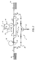
図1に示されるように電子写真再生装置10を参照して、イメージングドラム12が設けられ、この上には光伝導部材14がコーティングされている。前記イメージドラム12は、よく知られた駆動機構により(図示されず)、矢印で示される方向に選択的に回転され、前記光伝導部材14を前記電子写真再生装置の一連のサブシステムに通過させる。プライマリ荷電装置16が、前記光伝導部材14の上に均一な静電荷を堆積させるために設けられている。前記光伝導部材14の上の均一な静電荷は、引き続き、例えばデジタルアドレス化暴露装置18であって、例えば発光ダイオード(LED)アレイ又はレーザースキャンによって、再生されるべき電気的潜在イメージを形成すために選択的に消失される。電気的潜在イメージはその後、現像サブシステム20により可視化される。即ち、現像サブシステム20は、前記潜在イメージの電気荷電パターンに応じて荷電された顔料マーキング粒子を前記光伝導部材14上に堆積する。現像されたマーキング粒子イメージはその後レシーバ部材(また基板とも参照する)22に移される。レシーバ部材は、移動ベルト26上で供給24から供給される。前記光伝導部材14から前記レシーバ部材22への前記マーキング粒子を移動させる電場は、電気的にバイアスされたローラー28により供給される。クリーナ30は、前記光伝導部材14から前記レシーバ部材22へ移動されなかったすべてのマーキング粒子を除去する。前記マーキング粒子イメージを持つ前記レシーバ部材22はその後、溶融ローラー32とプレスローラー34の間に形成されるニップを通じて移動され、そこで前記マーキング粒子イメージは熱と圧力により前記レシーバ部材22に固定される。
As shown in FIG. 1, referring to the electrophotographic reproducing
溶融ローラー32は、前記レシーバ部材22に前記マーキング粒子を溶融させるに十分高い温度に加熱されている。前記レシーバ部材22が前記ニップ間を通過し、前記マーキング粒子イメージを持つ側で前記溶融ローラー32と接触する。前記溶融ニップを出た後、前記プリントジョブが前記レシーバ22の片側だけのイメージに関する場合には、出力スタック36に移動される。前記プリントジョブが前記レシーバ部材22の2つ(裏面)側のイメージにも関するものである場合(以下二重プリントとする)、前記レシーバ部材22は、前記出力スタック36には移動されず、むしろリターンパス38へ方向付けされる。リターンパス38では、レシーバ部材22は、ターンオーバ装置40によりターンオーバされ、移動ベルト26に戻される。そこで、第二のマーキング粒子イメージがレシーバ部材の第二の側に移される。レシーバ部材の第二の側にある前記マーキング粒子イメージはその後前記溶融ローラー32とプレスローラー34の間に形成されるニップを通って移動し、そこで前記レシーバ部材22の第二の側の前記マーキング粒子イメージが熱と圧力で前記レシーバ部材の第二の側に溶融される。前記溶融ニップを出た後、前記レシーバ部材は両側にイメージを持ち、出力スタック36へ移動される。
The fusing
図2は、図1の電子写真再生装置の一変形を示す。図2に記載の変形において、前記光伝導部材上に形成された前記マーキング粒子イメージは、最初中間的な移動要素に移され、その後前記中間的な移動要素から前記レシーバ部材に移される。図1及び図2に記載の2つの電子写真再生装置に共通するすべての要素は、同じ参照番号を付してある。図2に示される電子写真再生装置11を参照して、光伝導部材14がコーティングされたイメージングドラム12が準備される。前記イメージングドラム12は、よく知られた駆動機構により(図示されず)、矢印で示される方向に選択的に回転され、前記光伝導部材14を前記電子写真再生装置の一連のサブシステムを通過させる。プライマリ荷電装置16が、前記光伝導部材14の上に均一な静電荷を堆積させるために設けられている。前記光伝導部材14の上の均一な静電荷は、引き続き、例えばデジタルアドレス化暴露装置18であって、例えば発光ダイオード(LED)アレイ又はレーザースキャンによって、再生されるべき資料の電気的潜在イメージを形成すために選択的に消失される。
FIG. 2 shows a modification of the electrophotographic reproducing apparatus of FIG. In the variant according to FIG. 2, the marking particle image formed on the photoconductive member is first transferred to an intermediate moving element and then transferred from the intermediate moving element to the receiver member. All elements common to the two electrophotographic reproducing apparatuses shown in FIGS. 1 and 2 are given the same reference numerals. Referring to the electrophotographic reproducing apparatus 11 shown in FIG. 2, an
電気的潜在イメージはその後、現像サブシステム20により可視化される。即ち、現像サブシステム20は、前記潜在イメージの電気荷電パターンに応じて荷電された顔料マーキング粒子を前記光伝導部材14上に堆積する。堆積されたマーキング粒子イメージはその後、光伝導部材14から中間移動部材15に移される。マーキング粒子イメージを光伝導部材14から中間移動部材15に移すための電場は、中間移動部材15に供給される適切なバイアス電圧である。クリーナ30は、光伝導部材14から中間移動部材15へ移されなかったすべてのマーキング粒子を取り除く。マーキング粒子イメージはその後、中間移動部材15からレシーバ部材22に移される。レシーバ部材22は、移動ベルト26に乗り供給装置24から供給される。前記マーキング粒子が中間移動部材15から前記レシーバ部材22へ移動させる電場は、電気的にバイアスされたローラー28により供給される。クリーナ30は、中間移動部材15からレシーバ部材22へ移されなかったすべてのマーキング粒子を取り除く。前記マーキング粒子イメージを持つ前記レシーバ部材22はその後、溶融ローラー32とプレスローラー34の間に形成されるニップを通り移動され、そこで前記マーキング粒子イメージは熱及び圧力により前記レシーバ部材22に溶融される。
The electrical latent image is then visualized by the
前記溶融ローラー32は、前記レシーバ部材22に前記マーキング粒子を溶融させるに十分高い温度に加熱されている。前記レシーバ部材22が前記ニップ間を通過し、前記マーキング粒子イメージを持つ側で前記溶融ローラー32と接触する。前記溶融ニップを出た後、前記プリントジョブが前記レシーバ22の片側だけのイメージに関する場合には、出力スタック36に移動される。前記プリントジョブが前記レシーバ部材22の2つ(裏面)側のイメージにも関するものである場合(以下二重プリントとする)、前記レシーバ部材22は、前記出力スタック36には移動されず、むしろリターンパス38へ方向付けされる。リターンパス38では、レシーバ部材22は、ターンオーバ装置40によりターンオーバされ、移動ベルト26に戻される。そこで、第二のマーキング粒子イメージがレシーバ部材の第二の側に移される。レシーバ部材の第二の側にある前記マーキング粒子イメージはその後前記溶融ローラー32とプレスローラー34の間に形成されるニップを通って移動し、そこで前記レシーバ部材22の第二の側の前記マーキング粒子イメージが熱と圧力で前記レシーバ部材の第二の側に溶融される。前記溶融ニップを出た後、前記レシーバ部材は両側にイメージを持ち、出力スタック36へ移動される。
The melting
図1及び2に記載の電子写真再生装置10及び11において、それぞれ上で説明したとおり、前記光伝導部材14がコーティングされた前記イメージングドラム12、前記プライマリ荷電装置16、暴露サブシステム18、現像サブシステム20、電気的にバイアスされたローラー28、クリーナ30(及び装置11のクリーナ31を伴う中間移動部材15)は以後、イメージングモデュールと参照する。図1で示す電子写真再生装置10又は図2で示す電子写真再生装置11のいずれかは、前記移動ベルト26の長手方向に沿って連続的に複数の前記イメージングモデュールを含むことができる。この目的は、異なるそれぞれの色のマーキング粒子イメージを生成し前記レシーバ部材に、重なるレジスタで移動させることである。図3は、例えば4色の電子写真再生装置を示し、図2の装置11に応じて一般的に13で符号付けされる。これは、イメージングモデュールとしてそれぞれシアン(C)、マゼンタ(M)、イエロー(Y)及びブラック(K)のマーキング粒子(もちろん他のモデュール部材もまた本発明で使用するためには好ましい)を含むイメージングモデュールを持つ。図3では、図2で同じ要素に対応した前記イメージングモデュールでの個々のプロセス要素は、図2と同じく数字で表されているが、C、M、Y又はKを伴って表されている。
1 and 2, as described above, the
本発明のプロセスのステップ1は、第一の熱可塑性イメージを生成するために電子写真方法を用いる。プリントされた基板は好ましくは、絶縁部材であり熱的に安定な材料である。例えば、ポリイミドであるが他の材料例えばPET、ファイバガラス及び紙もまた含まれる。基板はホールを含んでいてよく、前記基板の裏側の電気的に接合され得る。 Step 1 of the process of the present invention uses an electrophotographic method to generate a first thermoplastic image. The printed substrate is preferably an insulating member and a thermally stable material. For example, polyimide but other materials such as PET, fiberglass and paper are also included. The substrate may include holes and may be electrically bonded to the back side of the substrate.
ステップ2では、トナーを用いてプリントされた前記電極を導電性の粒子又は粉末と接触させる。銅、スズ、スズメッキ銅又は銀粒子である金属粒子が好ましい。しかし導電性ポリマー粒子もまた含まれる。導電性粒子は粒子間の導電性を改良するために上にコーティングされていてもよい。金属粒子に導電性ポリマーをコーティングすることは、基板固定ステップでの粒子間の導電性パスを形成するであろう。導電性ポリマーは金属塩又はカーボンを導電性強化のために含んでいてよい。 In step 2, the electrode printed with toner is brought into contact with conductive particles or powder. Metal particles that are copper, tin, tin-plated copper or silver particles are preferred. However, conductive polymer particles are also included. The conductive particles may be coated on top to improve the conductivity between the particles. Coating the metal particles with a conductive polymer will form a conductive path between the particles in the substrate fixing step. The conductive polymer may contain a metal salt or carbon for enhancing conductivity.
ステップ3は、前記導電性粒子を、トーン化イメージがある領域にのみ固定することである。このステップで加熱されたトナーは接着剤として作用し、前記導電性粒子を前記トナーが存在する領域にのみ接着する。前記トナーが冷却されると、前記導電性粒子が基板に確実に付着される。圧力がまた、このステップで熱に加えて又は熱に代えて用いることが可能である。 Step 3 is to fix the conductive particles only in the area where the toned image is. The toner heated in this step acts as an adhesive, and adheres the conductive particles only to the area where the toner is present. When the toner is cooled, the conductive particles are reliably attached to the substrate. Pressure can also be used in addition to or in place of heat in this step.
ステップ4では、前記熱可塑性イメージに接着されなかった導電性粒子がその後真空、圧縮空気、回転ブラシ又は当該技術分野の熟練者によく知られた他の方法で除去される。 In step 4, the conductive particles not adhered to the thermoplastic image are then removed by vacuum, compressed air, a rotating brush or other methods well known to those skilled in the art.
ステップ5では、前記プリントされた基板は、場合により、標準の静電電子写真プロセスを用いて他のトナーでプリントされてもよい。そこでは、絶縁層が、続いて適用される配線要素(ステップ参照)に接触しない領域に前記導電電極上に適用される。前記第一のトナーイメージを前記第二のトナーイメージと登録するための最も適切な方法は、当技術分野で知られている方法を使用することができる。登録システムの一例はDE200410051293(Jan D. Boness,Ingo K.Dreher,Heiko Hunold,Karlheinz Peter,Stefan Schraderによる10ー20ー04出願)及びUS2008/0050132公開に記載されている。これらは引用により本明細書に一部となる。 In step 5, the printed substrate may optionally be printed with other toners using standard electrostatographic processes. There, an insulating layer is applied on the conductive electrode in a region not in contact with the subsequently applied wiring elements (see step). The most suitable method for registering the first toner image with the second toner image can use methods known in the art. An example of a registration system is described in DE 200410051293 (Jan D. Bones, Ingo K. Dreher, Heiko Hunold, Karl Heinz Peter, Stefan Schrader 10-2004 application) and US 2008/0050132 publication. These are hereby incorporated by reference.
ステップ6は、ステップ1及び又は場合によりステップ5で用いた前記トナーをクロスリンクすることである。前記ひとつ又は両方の層にあるトナーは場合により、熱(熱クロスリンク)又はUV光(UVクロスリンク)を、前記透明な又は準透明なプリント基板の裏側を通じてステップ1でプリントされたトナーに対して、およびステップ5でプリントされたトナーに対して直接に、適用することでクロスリンクされることができる。 Step 6 is to cross-link the toner used in step 1 and / or step 5 if necessary. The toner in the one or both layers optionally applies heat (thermal crosslink) or UV light (UV crosslink) to the toner printed in step 1 through the back side of the transparent or semi-transparent printed circuit board. And can be cross-linked by applying directly to the toner printed in step 5.
配線要素、例えば集積回路、抵抗及びキャパシタは、その後前記プリントされた基板に接着され、前記プリントされた電極の電極が、すべての当該技術分野で知られる方法を用いて前記配線要素の適切な電極と接触可能にされる。基板をカットし、必要ならならばそれを硬質ボードに適用する必要がある場合には、当該技術分野で知られる追加のステップが用いられる。 Wiring elements, such as integrated circuits, resistors and capacitors, are then glued to the printed substrate, and the electrodes of the printed electrodes are all suitable electrodes of the wiring elements using methods known in the art. Made contactable with. If it is necessary to cut the substrate and if necessary apply it to a rigid board, additional steps known in the art are used.
前記方法はまた、多層プリント配線を製造するために使用することができる。前記ステップ1ー6が、最終的には硬質又はフレキシブルであるプリント配線基板のそれぞれの層の組を形成するために使用される。前記基板は、好ましくはポリイミドである。前記基板はホールを含んでいてよい。かかるホールは基板の裏側への結合を可能とするものである。 The method can also be used to produce multilayer printed wiring. Steps 1-6 are used to form each set of layers of the printed wiring board that is ultimately rigid or flexible. The substrate is preferably polyimide. The substrate may include holes. Such holes are capable of coupling to the back side of the substrate.
ステップ5の少なくとも第二のプリントトナーはその後上で説明した通りクロスリンクされ、第二の導電層が設けられる際に粘着性とはならない。 At least the second print toner of step 5 is then cross-linked as described above and does not become tacky when the second conductive layer is provided.
これまでのステップはその後それぞれの配線層で繰り返され多層プリント配線基板を作り上げる。前記第一の一組の層を前記第二の一組の層に登録する適切な方法は当該技術分野において知られている。 The steps so far are then repeated for each wiring layer to create a multilayer printed wiring board. Suitable methods for registering the first set of layers with the second set of layers are known in the art.
例えば集積回路、抵抗及びキャパシタ等の配線要素はその後前記基板に接着され、前記プリントされた電極の電極が前記配線要素の適切な電極と接触させる。基板をカットし、必要ならならばそれを硬質ボードに適用する必要がある場合には、当該技術分野で知られる追加のステップが用いられる。 For example, wiring elements such as integrated circuits, resistors and capacitors are then bonded to the substrate and the electrodes of the printed electrodes are brought into contact with the appropriate electrodes of the wiring elements. If it is necessary to cut the substrate and if necessary apply it to a rigid board, additional steps known in the art are used.
前記説明した両方の方法において、前記プリント基板は続いて同様のステップを用いて裏表面にプリントし、配線要素を基板の両面側に設けることが可能となる。それぞれの側の結合は、基板がプリントされる前又はその後に形成されたホールを導電材料で埋めることで作られる。 In both of the described methods, the printed circuit board can then be printed on the back surface using similar steps, and wiring elements can be provided on both sides of the board. The bond on each side is made by filling the holes formed with conductive material before or after the substrate is printed.
実施例1:導電性トナーを上記説明したように銀粉末及びポリエステルを用いて製造した。トナーをフェライトキャリアと混合し現像剤とし、その12gを、交互極を持つ20個の磁石のコアを含む磁気電子写真現像装置の容器に付荷した。約0.5mmの横線を含む電子的潜在イメージを光レセプタ上に形成し、前記光レセプタを前記現像装置近くに配置した。現像されたイメージは静電的紙に移され、得られたイメージはジメチルクロリドの蒸気に暴露して溶融させる。前記線のひとつの上で1インチ離れた点での測定された抵抗値が約100Ωであることが分かった。 Example 1 A conductive toner was prepared using silver powder and polyester as described above. The toner was mixed with a ferrite carrier to form a developer, and 12 g of the toner was loaded into a container of a magneto-electrophotographic developing apparatus including 20 magnet cores having alternating poles. An electronic latent image including a horizontal line of about 0.5 mm was formed on the light receptor, and the light receptor was placed near the developing device. The developed image is transferred to electrostatic paper, and the resulting image is melted by exposure to dimethyl chloride vapor. The measured resistance at a point 1 inch apart on one of the lines was found to be about 100Ω.
実施例2:実施例1と同様であるが、前記イメージをオーブン中で溶融した。電気抵抗は同じであった。 Example 2: Same as Example 1, but the image was melted in an oven. The electrical resistance was the same.
実施例3:実施例2と同様であるが、オーブンでの溶融後、前記配線をホットプレート上に置き約100℃で加熱した。Kaplan−Hシートをその上に置き、前記シートを前記配線に対して手で押さえ付け、それによりフェロタイプした。冷却後Kaplan−Hシートを前記配線から剥がした。抵抗値は数十Ωに低下した。 Example 3 As in Example 2, but after melting in the oven, the wiring was placed on a hot plate and heated at about 100 ° C. A Kaplan-H sheet was placed thereon and the sheet was pressed against the wiring by hand, thereby ferrotyping. After cooling, the Kaplan-H sheet was peeled off from the wiring. The resistance value decreased to several tens of ohms.
実施例4:この実施例では、プリント配線は、電子写真的に形成された上で説明したパターン上に銀粉末を堆積することで形成した。具体的には、電子写真イメージは通常のトナーを用いて配線のパターンで形成された。前記イメージをオーブンで溶融した後、前記パターンを冷却し、その後銀粉末をコーティングした。粉末はジクロロメタンの蒸気を適用してパターンに粘着させた。過剰の銀粉末を、最初は基板の角を保持してタップすることで、さらに圧縮空気を吹き付けることで除去した。その後配線を上で説明したようにフェロタイプした。得られた抵抗は約数百Ωであった。 Example 4: In this example, the printed wiring was formed by depositing silver powder on the pattern described above which was formed electrophotographically. Specifically, the electrophotographic image was formed with a wiring pattern using ordinary toner. After the image was melted in an oven, the pattern was cooled and then coated with silver powder. The powder was adhered to the pattern by applying dichloromethane vapor. Excess silver powder was removed by first tapping while holding the corners of the substrate and then spraying with compressed air. The wiring was then ferrotyped as described above. The obtained resistance was about several hundred Ω.
実施例5:この実施例は実施例4と同様であるが、前記粘着及び除去後に、銀粉末を数回追加コーティングして堆積させた。それぞれの粘着後銀を上で説明したように除去した。最後にフェロタイプ後、得られた抵抗値は100Ωよりも小さかった。 Example 5: This example is similar to Example 4, but after the sticking and removal, silver powder was additionally coated several times and deposited. Each post-adhesion silver was removed as described above. Finally, after ferrotyping, the obtained resistance value was less than 100Ω.
Claims (21)
基板上に熱可塑性物質を含むパターンをイメージに基づき生成し;
前記基板上に導電性粉末を堆積させ;及び
前記導電性粉末を前記熱可塑性基板上に恒久的に固定し;
前記熱可塑性パターンでコーティングされた以外の基板の部分から前記導電性粉末を除去する、ステップを含む方法。 A method of manufacturing printed wiring:
Generating a pattern comprising a thermoplastic material on the substrate based on the image;
Depositing conductive powder on the substrate; and permanently fixing the conductive powder on the thermoplastic substrate;
Removing the conductive powder from portions of the substrate other than coated with the thermoplastic pattern.
プライマリイメージ部材を荷電し;
前記プライマリイメージ部材にイメージに基づく暴露により静電的潜在イメージを生成し;
前記プライマリイメージ部材上に熱可塑性粒子をイメージに基づき堆積し;
前記熱可塑性粒子を、電気的絶縁基板に移し;
前記基板上に導電性粉末を堆積し;
前記導電性粉末を前記基板上に恒久的に固定し;及び
前記熱可塑性パターンでコーティングされていない他の基板の部分から前記導電性粉末を除去する、ステップを含む方法。 A method of manufacturing printed wiring:
Charging the primary image member;
Generating an electrostatic latent image by image-based exposure to the primary image member;
Depositing thermoplastic particles based on the image on the primary image member;
Transferring the thermoplastic particles to an electrically insulating substrate;
Depositing conductive powder on the substrate;
Permanently fixing the conductive powder on the substrate; and removing the conductive powder from portions of the other substrate not coated with the thermoplastic pattern.
プライマリイメージ部材を荷電し;
前記プライマリイメージ部材にイメージに基づく暴露により静電的潜在イメージを生成し;
前記プライマリイメージ部材上に熱可塑性粒子をイメージに基づき堆積し;
前記熱可塑性粒子を、電気的絶縁基板に移し;
前記導電性粉末を前記基板上に恒久的に固定し;
前記基板上に導電性粉末を堆積し;
前記導電性粉末を前記基板上に恒久的に固定し;
前記熱可塑性パターンでコーティングされていない他の基板の部分から前記導電性粉末を除去し、及び
前記導電性粒子を、熱及び/又は圧力により前記熱可塑性物質中に入れ込む、ステップを含む方法。 A method of manufacturing printed wiring:
Charging the primary image member;
Generating an electrostatic latent image by image-based exposure to the primary image member;
Depositing thermoplastic particles based on the image on the primary image member;
Transferring the thermoplastic particles to an electrically insulating substrate;
Permanently fixing the conductive powder on the substrate;
Depositing conductive powder on the substrate;
Permanently fixing the conductive powder on the substrate;
Removing the conductive powder from other portions of the substrate not coated with the thermoplastic pattern, and entraining the conductive particles into the thermoplastic material by heat and / or pressure.
プライマリイメージ部材に荷電し;
前記イメージをイメージに基づき暴露して静電潜在イメージを生成し;
前記プライマリイメージ部材上に熱可塑性粒子をイメージに基づき堆積させ;
前記熱可塑性粒子を電気的に絶縁される基板に移し;
前記熱可塑性粒子を恒久的に固定し;
前記基板上に導電性粉末を堆積し;
前記導電性粉末を前記熱可塑性基板に恒久的に固定し;及び
前記熱可塑性イメージにコーティングされた以外の基板の他の部分から金属粉末を除去し;
電気的絶縁性熱可塑性粒子を、前記基板上に均一に堆積させ;
前記熱可塑性粒子をクロスリンクさせて熱硬化層とし;
プライマリイメージング部材を荷電し;
前記プライマリイメージ部材をイメージに基づき暴露して静電的潜在イメージを生成し;
前記プライマリイメージ部材に熱可塑性粒子をイメージに基づき堆積させ;
前記熱可塑性粒子を前記熱硬化層に移し、前記以前に移された導電性粒子を登録し;
前記熱可塑性粒子恒久的に固定し;
前記基板上に導電性粉末を堆積させ;
前記導電性粉末を前記熱可塑性基板上に恒久的に固定し;及び
前記熱可塑性パターンにコーティングされていない前記基板の部分から導電性粉末を除去する、ステップを含む方法。 A method of manufacturing printed wiring:
The primary image member is charged;
Exposing the image based on the image to generate an electrostatic latent image;
Depositing thermoplastic particles on the primary image member based on the image;
Transferring the thermoplastic particles to an electrically insulated substrate;
Permanently fixing the thermoplastic particles;
Depositing conductive powder on the substrate;
Permanently fixing the conductive powder to the thermoplastic substrate; and removing metal powder from other portions of the substrate other than coated with the thermoplastic image;
Electrically insulating thermoplastic particles are uniformly deposited on the substrate;
Cross-linking the thermoplastic particles to form a thermoset layer;
Charging the primary imaging member;
Exposing the primary image member based on an image to generate an electrostatic latent image;
Depositing thermoplastic particles on the primary image member based on the image;
Transferring the thermoplastic particles to the thermosetting layer and registering the previously transferred conductive particles;
Permanently fixing the thermoplastic particles;
Depositing conductive powder on the substrate;
Permanently fixing the conductive powder on the thermoplastic substrate; and removing the conductive powder from a portion of the substrate that is not coated with the thermoplastic pattern.
Applications Claiming Priority (3)
| Application Number | Priority Date | Filing Date | Title |
|---|---|---|---|
| US12/341,099 US8512933B2 (en) | 2008-12-22 | 2008-12-22 | Method of producing electronic circuit boards using electrophotography |
| US12/341,099 | 2008-12-22 | ||
| PCT/US2009/006541 WO2010090631A1 (en) | 2008-12-22 | 2009-12-14 | Method of producing electronic circuit boards using electrophotography |
Publications (2)
| Publication Number | Publication Date |
|---|---|
| JP2012513672A true JP2012513672A (en) | 2012-06-14 |
| JP2012513672A5 JP2012513672A5 (en) | 2013-01-10 |
Family
ID=42154701
Family Applications (1)
| Application Number | Title | Priority Date | Filing Date |
|---|---|---|---|
| JP2011542124A Withdrawn JP2012513672A (en) | 2008-12-22 | 2009-12-14 | Electronic circuit board manufacturing method using electrophotography |
Country Status (5)
| Country | Link |
|---|---|
| US (2) | US8512933B2 (en) |
| EP (1) | EP2368412A1 (en) |
| JP (1) | JP2012513672A (en) |
| CN (1) | CN102265713A (en) |
| WO (1) | WO2010090631A1 (en) |
Cited By (1)
| Publication number | Priority date | Publication date | Assignee | Title |
|---|---|---|---|---|
| KR101515952B1 (en) | 2013-06-19 | 2015-04-29 | 난창 오-필름 테크 컴퍼니 리미티드 | Apparatus for substratedouble-surface hole-filling |
Families Citing this family (8)
| Publication number | Priority date | Publication date | Assignee | Title |
|---|---|---|---|---|
| GB2452320B (en) * | 2007-09-03 | 2012-04-11 | Dek Int Gmbh | Workpiece processing system and method |
| KR101941679B1 (en) * | 2010-10-14 | 2019-01-24 | 스토라 엔소 오와이제이 | Method and arrangement for attaching a chip to a printed conductive surface |
| US9465346B2 (en) | 2014-06-24 | 2016-10-11 | Kabushiki Kaisha Toshiba | Metallic color image forming apparatus and metallic color image forming method |
| SE539800C2 (en) * | 2015-05-26 | 2017-12-05 | Stora Enso Oyj | Method and arrangement for producing electrically conductivepatterns on substrates |
| US20170044416A1 (en) | 2015-08-10 | 2017-02-16 | Delavan Inc | Particulates for additive manufacturing techniques |
| EP3414627A1 (en) | 2016-03-31 | 2018-12-19 | Hp Indigo B.V. | Photoconductor charging uniformity correction |
| US10682703B2 (en) * | 2017-11-07 | 2020-06-16 | Aaron Roni Shafir | Systems and methods for delivering materials for printing three dimensional (3D) objects |
| KR102308296B1 (en) * | 2018-10-05 | 2021-10-01 | 가부시끼가이샤 마에가와 세이사꾸쇼 | Clamping device for bony leg meat, inserting device for bony leg meat, and clamping method for bony leg meat |
Family Cites Families (15)
| Publication number | Priority date | Publication date | Assignee | Title |
|---|---|---|---|---|
| GB1095117A (en) * | 1963-12-26 | 1967-12-13 | Matsushita Electric Ind Co Ltd | Method of making printed circuit board |
| US3997344A (en) * | 1974-07-05 | 1976-12-14 | American Can Company | Dry positive photopolymer imaging process involving heating and application of toner |
| JP4680362B2 (en) * | 2000-09-22 | 2011-05-11 | 株式会社石井工作研究所 | Electronic component manufacturing method and manufacturing apparatus |
| WO2002048980A1 (en) * | 2000-12-15 | 2002-06-20 | Electrox Corp. | Process for the manufacture of novel, inexpensive radio frequency identification devices |
| JP2004048030A (en) * | 2002-07-15 | 2004-02-12 | Toshiba Corp | Method of manufacturing electronic circuit and device for manufacturing the electronic circuit |
| US7051429B2 (en) * | 2003-04-11 | 2006-05-30 | Eastman Kodak Company | Method for forming a medium having data storage and communication capabilities |
| US6872500B2 (en) * | 2003-08-26 | 2005-03-29 | Eastman Kodak Company | Method of patterning an electroconductive layer on a support |
| US7163734B2 (en) * | 2003-08-26 | 2007-01-16 | Eastman Kodak Company | Patterning of electrically conductive layers by ink printing methods |
| US6893790B2 (en) * | 2003-08-26 | 2005-05-17 | Eastman Kodak Company | Photopatterning of conductive electrode layers containing electrically-conductive polymer particles |
| US7033713B2 (en) * | 2003-08-26 | 2006-04-25 | Eastman Kodak | Electrographic patterning of conductive electrode layers containing electrically-conductive polymeric materials |
| JP2005203396A (en) * | 2004-01-13 | 2005-07-28 | Toshiba Corp | Electronic component and method and apparatus for manufacturing the same |
| JP3947776B2 (en) * | 2004-05-13 | 2007-07-25 | ニスカ株式会社 | Conductive material and manufacturing method thereof |
| US7593656B2 (en) * | 2004-10-20 | 2009-09-22 | Eastman Kodak Company | Method and device for controlling registration |
| US20070218258A1 (en) * | 2006-03-20 | 2007-09-20 | 3M Innovative Properties Company | Articles and methods including patterned substrates formed from densified, adhered metal powders |
| US20090145548A1 (en) * | 2007-12-08 | 2009-06-11 | Chien-Han Ho | Method Of Forming Printed Circuit By Printing Method |
-
2008
- 2008-12-22 US US12/341,099 patent/US8512933B2/en not_active Expired - Fee Related
-
2009
- 2009-12-14 EP EP09801588A patent/EP2368412A1/en not_active Withdrawn
- 2009-12-14 JP JP2011542124A patent/JP2012513672A/en not_active Withdrawn
- 2009-12-14 CN CN2009801521821A patent/CN102265713A/en active Pending
- 2009-12-14 WO PCT/US2009/006541 patent/WO2010090631A1/en active Application Filing
-
2012
- 2012-09-14 US US13/616,558 patent/US8497057B2/en not_active Expired - Fee Related
Cited By (1)
| Publication number | Priority date | Publication date | Assignee | Title |
|---|---|---|---|---|
| KR101515952B1 (en) | 2013-06-19 | 2015-04-29 | 난창 오-필름 테크 컴퍼니 리미티드 | Apparatus for substratedouble-surface hole-filling |
Also Published As
| Publication number | Publication date |
|---|---|
| US20100159373A1 (en) | 2010-06-24 |
| CN102265713A (en) | 2011-11-30 |
| US8512933B2 (en) | 2013-08-20 |
| US20130004892A1 (en) | 2013-01-03 |
| EP2368412A1 (en) | 2011-09-28 |
| US8497057B2 (en) | 2013-07-30 |
| WO2010090631A1 (en) | 2010-08-12 |
Similar Documents
| Publication | Publication Date | Title |
|---|---|---|
| US8497057B2 (en) | Method of producing electronic circuit boards using electrophotography | |
| US20100155128A1 (en) | Printed electronic circuit boards and other articles having patterned coonductive images | |
| US8661661B2 (en) | Process for the production of a circuit portion on a substrate | |
| US11206738B2 (en) | Method and apparatus for forming on a substrate a pattern of a material | |
| KR20090024771A (en) | System and method for making printed electronic circuits using electrophotography | |
| US20100159648A1 (en) | Electrophotograph printed electronic circuit boards | |
| US5011758A (en) | Use of a liquid electrophotographic toner with an overcoated permanent master in electrostatic transfer | |
| US20050227161A1 (en) | Image forming apparatus and method of manufacturing electronic circuit using the same | |
| US5416569A (en) | Electrographically making devices having electrically conductive paths corresponding to those graphically represented on a mask | |
| US8580331B2 (en) | Digital manufacture of an electrical circuit | |
| JPS6344314B2 (en) | ||
| JPH02132463A (en) | Preparation of color-toned pattern on image receiving surface isolated electrically | |
| JP4134372B2 (en) | Chargeable powder for circuit formation, circuit pattern forming method using the same, and multilayer wiring board formed thereby | |
| JP3909728B2 (en) | Printed wiring board manufacturing equipment | |
| JPH11272125A (en) | Electrophotographic device | |
| AU603108B2 (en) | Permanent master with a persistent latent image for use in electrostatic transfer to a receiving substrate | |
| EP0252735B1 (en) | Yethod of high resolution electrostatic transfer of a high density image to a nonporous and nonabsorbent conductive substrate | |
| JPH06252532A (en) | Manufacture of wiring board | |
| CA1295652C (en) | Method of high resolution electrostatic transfer of a high density image to a nonporous and nonabsorbent conductive substrate | |
| JP2023027634A (en) | Electrostatic printing method | |
| JP2009094440A (en) | Manufacturing device and manufacturing method for wiring material using electrophotographic method | |
| JPH02288392A (en) | Method of toned pattern on image pickup plane which is electrically isolated | |
| JPS6329597A (en) | High resolution electrostatic transcription of high density picture | |
| JPH11340607A (en) | Method for forming circuit and multilayer wiring substrate formed there by | |
| JPH02250073A (en) | High resolution electrostatic transfer method for high density image |
Legal Events
| Date | Code | Title | Description |
|---|---|---|---|
| A521 | Request for written amendment filed |
Free format text: JAPANESE INTERMEDIATE CODE: A523 Effective date: 20121113 |
|
| A621 | Written request for application examination |
Free format text: JAPANESE INTERMEDIATE CODE: A621 Effective date: 20121113 |
|
| A761 | Written withdrawal of application |
Free format text: JAPANESE INTERMEDIATE CODE: A761 Effective date: 20130424 |