JP2012511285A - Switching voltage regulator with frequency selection - Google Patents
Switching voltage regulator with frequency selection Download PDFInfo
- Publication number
- JP2012511285A JP2012511285A JP2011539765A JP2011539765A JP2012511285A JP 2012511285 A JP2012511285 A JP 2012511285A JP 2011539765 A JP2011539765 A JP 2011539765A JP 2011539765 A JP2011539765 A JP 2011539765A JP 2012511285 A JP2012511285 A JP 2012511285A
- Authority
- JP
- Japan
- Prior art keywords
- frequency
- switcher
- voltage regulator
- switching voltage
- jammer
- Prior art date
- Legal status (The legal status is an assumption and is not a legal conclusion. Google has not performed a legal analysis and makes no representation as to the accuracy of the status listed.)
- Pending
Links
Images


Classifications
-
- H—ELECTRICITY
- H04—ELECTRIC COMMUNICATION TECHNIQUE
- H04B—TRANSMISSION
- H04B1/00—Details of transmission systems, not covered by a single one of groups H04B3/00 - H04B13/00; Details of transmission systems not characterised by the medium used for transmission
- H04B1/06—Receivers
- H04B1/10—Means associated with receiver for limiting or suppressing noise or interference
-
- G—PHYSICS
- G05—CONTROLLING; REGULATING
- G05F—SYSTEMS FOR REGULATING ELECTRIC OR MAGNETIC VARIABLES
- G05F1/00—Automatic systems in which deviations of an electric quantity from one or more predetermined values are detected at the output of the system and fed back to a device within the system to restore the detected quantity to its predetermined value or values, i.e. retroactive systems
- G05F1/10—Regulating voltage or current
-
- H—ELECTRICITY
- H02—GENERATION; CONVERSION OR DISTRIBUTION OF ELECTRIC POWER
- H02M—APPARATUS FOR CONVERSION BETWEEN AC AND AC, BETWEEN AC AND DC, OR BETWEEN DC AND DC, AND FOR USE WITH MAINS OR SIMILAR POWER SUPPLY SYSTEMS; CONVERSION OF DC OR AC INPUT POWER INTO SURGE OUTPUT POWER; CONTROL OR REGULATION THEREOF
- H02M1/00—Details of apparatus for conversion
- H02M1/44—Circuits or arrangements for compensating for electromagnetic interference in converters or inverters
-
- H—ELECTRICITY
- H02—GENERATION; CONVERSION OR DISTRIBUTION OF ELECTRIC POWER
- H02M—APPARATUS FOR CONVERSION BETWEEN AC AND AC, BETWEEN AC AND DC, OR BETWEEN DC AND DC, AND FOR USE WITH MAINS OR SIMILAR POWER SUPPLY SYSTEMS; CONVERSION OF DC OR AC INPUT POWER INTO SURGE OUTPUT POWER; CONTROL OR REGULATION THEREOF
- H02M3/00—Conversion of dc power input into dc power output
- H02M3/02—Conversion of dc power input into dc power output without intermediate conversion into ac
- H02M3/04—Conversion of dc power input into dc power output without intermediate conversion into ac by static converters
- H02M3/10—Conversion of dc power input into dc power output without intermediate conversion into ac by static converters using discharge tubes with control electrode or semiconductor devices with control electrode
- H02M3/145—Conversion of dc power input into dc power output without intermediate conversion into ac by static converters using discharge tubes with control electrode or semiconductor devices with control electrode using devices of a triode or transistor type requiring continuous application of a control signal
- H02M3/155—Conversion of dc power input into dc power output without intermediate conversion into ac by static converters using discharge tubes with control electrode or semiconductor devices with control electrode using devices of a triode or transistor type requiring continuous application of a control signal using semiconductor devices only
- H02M3/156—Conversion of dc power input into dc power output without intermediate conversion into ac by static converters using discharge tubes with control electrode or semiconductor devices with control electrode using devices of a triode or transistor type requiring continuous application of a control signal using semiconductor devices only with automatic control of output voltage or current, e.g. switching regulators
-
- H—ELECTRICITY
- H04—ELECTRIC COMMUNICATION TECHNIQUE
- H04B—TRANSMISSION
- H04B15/00—Suppression or limitation of noise or interference
Abstract
スイッチング電圧レギュレータのスイッチャ周波数をインテリジェントに変えることにより、スイッチング電圧レギュレータからの干渉を軽減するための技術が提供される。一態様では、スイッチャ周波数は、プログラマブル・クロック・ディバイダへの周波数セッティング入力を調整することにより設定される。さらなる態様では、プロセッサは、スイッチング電圧レギュレータに対しての所望のスイッチャ周波数を生成するための基準クロック周波数信号を分周するためのディバイディングファクタを表す値を受け取るプログラマブル・クロック・ディバイダを駆動する。プログラマブル・クロック・ディバイダの値は、最適なパフォーマンスを達成し、そして、所定の動作状態に対してのスイッチャ周波数スプリアス成分の効果を軽減するために、選択的に変更される。 Techniques are provided for mitigating interference from a switching voltage regulator by intelligently changing the switcher frequency of the switching voltage regulator. In one aspect, the switcher frequency is set by adjusting a frequency setting input to the programmable clock divider. In a further aspect, the processor drives a programmable clock divider that receives a value representing a dividing factor for dividing the reference clock frequency signal to generate a desired switcher frequency for the switching voltage regulator. The value of the programmable clock divider is selectively changed to achieve optimal performance and reduce the effect of the switcher frequency spurious component on a given operating condition.
Description
本開示は一般には集積回路に関わり、より詳細には無線通信デバイス内のスイッチング電圧レギュレータに関する。 The present disclosure relates generally to integrated circuits, and more particularly to switching voltage regulators in wireless communication devices.
無線通信デバイスは、電源供給のために電池または外部DC電源を必要とする。無線通信デバイス内には複数の集積回路(ICs)がある。これらのICsは、通常は、無線通信デバイスに取り付けられた電池(battery)または外部DC電源よりもずっと低いDC電圧で動作する。低動作電圧での集積回路動作を容易にするために、外部DC電源または電池の電圧を集積回路の低電圧に変化するためのスイッチング電圧レギュレータが普通は必要とされる。 Wireless communication devices require a battery or an external DC power source for power supply. There are multiple integrated circuits (ICs) within a wireless communication device. These ICs typically operate at a much lower DC voltage than a battery or external DC power source attached to the wireless communication device. To facilitate integrated circuit operation at low operating voltages, a switching voltage regulator is usually required to change the voltage of the external DC power supply or battery to the low voltage of the integrated circuit.
スイッチング電圧レギュレータは、電池電圧(VBAT)と集積回路供給電圧(VDD)との差が数百ミリボルトよりも大きい時に、最も高い出力効率を提供する。一つの特定の例においては、電池は公称電圧3.6のLiイオンセルからなり、そして、集積回路は1.8Vで動作する。したがって、電池電圧と集積回路電圧との差は、3.6V−1.8V、つまり、1.8Vである。この特定の例においては、スイッチング電圧レギュレータは線形レギュレータ上において強く好ましい。線形レギュレータは電池と負荷との間で、まる1.8Vの降下を経験するであろう。線形レギュレータで消費される電力は1.8V*IDD(集積回路の負荷電流)である。それ自体としてはスイッチング電圧レギュレータは(負荷電流のワイドレンジ上で)集積回路で使用されるエネルギーのたった10%を消費し得るが、線形レギュレータは負荷電流にかかわらず集積回路で使用されるエネルギーの100%を消費するであろう。このような理由のため、スイッチング電圧レギュレータはしばしば無線通信デバイス内に使用される。 Switching voltage regulators provide the highest output efficiency when the difference between the battery voltage (VBAT) and the integrated circuit supply voltage (VDD) is greater than a few hundred millivolts. In one particular example, the battery consists of a Li-ion cell with a nominal voltage of 3.6 and the integrated circuit operates at 1.8V. Therefore, the difference between the battery voltage and the integrated circuit voltage is 3.6V-1.8V, that is, 1.8V. In this particular example, a switching voltage regulator is strongly preferred over a linear regulator. The linear regulator will experience a full 1.8V drop between the battery and the load. The power consumed by the linear regulator is 1.8V * IDD (integrated circuit load current). As such, switching voltage regulators can consume only 10% of the energy used in an integrated circuit (over a wide range of load currents), whereas linear regulators consume the energy used in an integrated circuit regardless of load current. 100% will be consumed. For this reason, switching voltage regulators are often used in wireless communication devices.
スイッチング電圧レギュレータは、高い(higher)外部DC電源電圧と低い(lower)集積回路電圧との間でエネルギーを伝達するために、エネルギー貯蔵デバイス(インダクタまたはキャパシタ)と連動して一つまたは複数の電子スイッチを用いて、高い(higher)入力電圧と低い(lower)出力電圧との間で変換し得る。 A switching voltage regulator works with an energy storage device (inductor or capacitor) to transfer energy between a higher external DC power supply voltage and a lower integrated circuit voltage. A switch can be used to convert between a higher input voltage and a lower output voltage.
背景として、スイッチング電圧レギュレータ出力電圧(Vo)とスイッチング電圧レギュレータ入力電圧(Vi)との間の比は、スイッチング電圧レギュレータのためにデューティサイクル(D=Vo/Vi)をセットする。スイッチング電圧レギュレータ周波数は、出力電圧リップル要求、スイッチング電圧レギュレータ内の直列のインダクタおよび負荷フィルタリングキャパシタのサイズ、出力DC負荷電流、および、スイッチング電圧レギュレータの所望の電力効率によって規定される(dictated)。スイッチング電圧レギュレータが他の無線周波数(RF)トランシーバ回路に結合される場合、スイッチング電圧レギュレータのスイッチャ周波数は無線通信デバイス内の他のそのようなコンポーネントに干渉をもたらすことができる。この干渉はVDDおよびRFトランシーバ回路のアース接続上の電圧リップルとして現れる。この電圧リップルは離散周波数コンポーネント(components)からなる。各周波数コンポーネントはスイッチング電圧レギュレータのスイッチャ周波数の調波(harmonic)である。各調波の電力レベルは、(i)スイッチング電圧レギュレータのスイッチャ周波数のディーティサイクル、(ii)出力電圧の容量性フィタリングの程度、さらに、(iii)スイッチング電圧レギュレータとRFトランシーバ回路との間のカップリングのタイプに依存する。 By way of background, the ratio between the switching voltage regulator output voltage (Vo) and the switching voltage regulator input voltage (Vi) sets the duty cycle (D = Vo / Vi) for the switching voltage regulator. The switching voltage regulator frequency is dictated by the output voltage ripple requirements, the size of the series inductor and load filtering capacitor in the switching voltage regulator, the output DC load current, and the desired power efficiency of the switching voltage regulator. If the switching voltage regulator is coupled to other radio frequency (RF) transceiver circuits, the switcher frequency of the switching voltage regulator can cause interference to other such components in the wireless communication device. This interference appears as a voltage ripple on the ground connection of the VDD and RF transceiver circuits. This voltage ripple consists of discrete frequency components. Each frequency component is a harmonic of the switching voltage regulator's switcher frequency. The power level of each harmonic is: (i) the duty cycle of the switching voltage regulator's switcher frequency, (ii) the degree of capacitive filtering of the output voltage, and (iii) between the switching voltage regulator and the RF transceiver circuit. Depends on coupling type.
無線周波数(RF)電圧制御オシレータ(複数)(VCOs)は一般にはRFトランシーバ回路内に組み込まれ、そして、通信信号(複数)をベースバンドから/へ(from/to)RFに/からに(to/from)アップコンバートまたはダウンコンバートするためのローカルオシレータ(複数)(LOs)として機能する。RF VCOに直接的または間接的に結合されたスイッチング電圧レギュレータを有する典型的なコンフィギュレーションにおいては、スイッチング電圧レギュレータの出力での電圧リップルは、スイッチング電圧レギュレータ周波数の調波に等しいオフセットでRF VCO出力上に周波数変調(FM)を作成するために、RF VCOの周波数同調素子電圧(frequency tuning element voltage)にコンバインし得る。スイッチング電圧レギュレータ誘発のRF VCO上のFMは、調波スプリアス・コンテント(harmonic spurious content)をRF VCOの基本出力キャリア周波数からのオフセットに出現させる。 Radio frequency (RF) voltage controlled oscillators (VCOs) are typically incorporated within an RF transceiver circuit and route communication signals from / to baseband to / from RF. / from) Acts as local oscillators (LOs) for up-converting or down-converting. In a typical configuration with a switching voltage regulator coupled directly or indirectly to the RF VCO, the voltage ripple at the output of the switching voltage regulator is offset at an offset equal to the harmonic of the switching voltage regulator frequency. To create frequency modulation (FM) on top, it can be combined with the frequency tuning element voltage of the RF VCO. An FM on a switching voltage regulator-induced RF VCO causes harmonic spurious content to appear at an offset from the fundamental output carrier frequency of the RF VCO.
スイッチング電圧レギュレータにより誘起された、この(RF VCOに直接またはRF VCOに結合された)調波スプリアス・コンテントは、ある動作条件下では、無線通信デバイスのパフォーマンスに干渉し得る。例えば、弱い受信強度、所望の受信チャンネルからの特定周波数オフセットでの外部ジャマーの存在、および/または、フルデュープレックストランシーバ(full-duplex transceiver)内の受信パスへの送信漏れは全て、スイッチング電圧レギュレータの存在下で、無線周波数(radio frequencies)へまたはから(to or from)、にアップまたはダウン−コンバートされるアナログ信号上でより大きな(greater)干渉の寄与することができる。 This harmonic spurious content (directly coupled to the RF VCO or coupled to the RF VCO) induced by the switching voltage regulator can interfere with the performance of the wireless communication device under certain operating conditions. For example, weak reception strength, the presence of external jammers at a specific frequency offset from the desired receive channel, and / or transmission leakage to the receive path in a full-duplex transceiver are all in the switching voltage regulator In the presence, greater interference contributions can be made on analog signals that are up- or down-converted to or from radio frequencies.
無線通信デバイス内のスイッチング電圧レギュレータによって生じたスイッチング周波数スプリアス・コンテントの効果を低減するための周知の方法は、(i)パルス幅変調、パルス密度変調、または、周波数ホッピングを用いて、スイッチング電圧レギュレータの周波数を連続的に調整すること; b)無線通信デバイスの受信オンリーモード(receive only modes)の期間にスイッチング電圧レギュレータと線形レギュレータとを切り替えること(toggling); および(iii)敏感なVCOおよび他のコンポーネントからできるだけ遠くにスイッチング電圧レギュレータを(改善されたアイソレーションのためにシールディングおよび差動信号パスを用いて)動かすことを含み、これらの全てはあるレベルの設計複雑さ(design complexity)、または、回路ボードまたは周回路エリアの能率的でない利用を導入する。 Known methods for reducing the effects of switching frequency spurious content caused by switching voltage regulators in wireless communication devices include: (i) using pulse width modulation, pulse density modulation, or frequency hopping, and switching voltage regulators B) toggling between a switching voltage regulator and a linear regulator during the receive only modes of the wireless communication device; and (iii) sensitive VCOs and others Including moving the switching voltage regulator (using shielding and differential signal paths for improved isolation) as far as possible from the components of the system, all of which have a certain level of design complexity, Or Introducing inefficient use of circuit boards or circuit areas.
従来の技術に不利益を与えずに無線通信デバイス内のスイッチング電圧レギュレータから干渉の効果を低減するための改良方法(improved way)が要求される。 What is needed is an improved way to reduce the effects of interference from switching voltage regulators in wireless communication devices without penalizing the prior art.
スイッチング電圧レギュレータのスイッチャ周波数をインテリジェントに変えることにより、スイッチング電圧レギュレータからの干渉を軽減するための技術が提供される。一態様では、スイッチャ周波数は、プログラマブル・クロック・ディバイダ(programmable clock divider)への周波数セッティング入力を調整することにより設定される。さらなる態様では、プロセッサは、スイッチング電圧レギュレータに対しての所望のスイッチャ周波数を生成するための基準クロック周波数信号を分周するためのディバイディングファクタ(dividing factor)を表す値を受け取るプログラマブル・クロック・ディバイダを駆動する。プログラマブル・クロック・ディバイダの値は、最適なパフォーマンスを達成し、そして、所定の動作状態に対してのスイッチャ周波数スプリアス成分(switcher frequency spurious content)の効果を軽減するために、選択的に変更される。 Techniques are provided for mitigating interference from a switching voltage regulator by intelligently changing the switcher frequency of the switching voltage regulator. In one aspect, the switcher frequency is set by adjusting a frequency setting input to a programmable clock divider. In a further aspect, the processor receives a value representing a dividing factor for dividing the reference clock frequency signal to generate a desired switcher frequency for the switching voltage regulator. Drive. Programmable clock divider values are selectively changed to achieve optimal performance and reduce the effect of switcher frequency spurious content on a given operating state .
本開示のさまざまな他の態様および実施形態は以下にさらに詳細に説明される。 Various other aspects and embodiments of the disclosure are described in further detail below.
前記概要は、全範囲の代表および本開示の範囲であるとの意図もなく、また、そう解釈されるべきでもなく、これらと追加の態様は、詳細な説明から、特に添付した図面と結合された時には、より容易に明確になるであろう。 The above summary is not intended to be, and should not be construed, as being representative of the full scope and scope of the disclosure, and these and additional aspects are combined from the detailed description, particularly with the accompanying drawings. It will be clearer more easily.
理解を容易にするために、図面において共通の同じ要素を示すことが可能の場合、このような要素を区別するために添字が追加されることが適切であるときを除いて、同じ参照数字が用いられる。図面内のイメージは例証のために簡略され、必ずしも縮尺通りに描かれてはない。 For ease of understanding, where it is possible to show the same common elements in the drawings, the same reference numerals are used unless it is appropriate to add subscripts to distinguish such elements. Used. The images in the drawings are simplified for purposes of illustration and are not necessarily drawn to scale.
添付した図面は本開示の代表的なコンフィギュレーションを例証し、そして、そのようなことで、他の同様に有効なコンフィギュレーションを認め得る本開示の範囲を限定するとはみなされるべきではない。したがって、詳説が無くても、いくつかのコンフィギュレーションの特徴(features)は他のコンフィギュレーション内に有利に組み込まれ得ると考えられる。 The accompanying drawings illustrate exemplary configurations of the present disclosure, and as such should not be construed to limit the scope of the present disclosure in which other equally valid configurations may be recognized. Thus, it is believed that some configuration features may be advantageously incorporated within other configurations without detailed description.
本明細書に述べられるデバイスはセルラ(cellular)、PCSおよびIMTなどのさまざまな無線通信周波数バンドならびにCDMA、TDMA、FDMA、OFDMAおよびSC−FDMAなどの無線インターファースに使用可能である。セルラ、PCSまたはIMTネットワーク標準および周波数バンドに加えて、このデバイスはローカル-エリアまたはパーソナル-エリアネットワーク標準、WLAN、Bluetooth(登録商標)およびウルトラ-ワイドバンド(ultra-wideband(UWB))に使用され得る。 The devices described herein can be used for various wireless communication frequency bands such as cellular, PCS and IMT, and wireless interfaces such as CDMA, TDMA, FDMA, OFDMA and SC-FDMA. In addition to cellular, PCS or IMT network standards and frequency bands, this device is used for local-area or personal-area network standards, WLAN, Bluetooth® and ultra-wideband (UWB). obtain.
示されるように図1は本実施形態に従う無線通信デバイス10のブロック図である。無線通信デバイス10は、RFフロント-エンド14に接続された無線周波数(RF)アンテナ12を含む。RFフロント-エンド14は、送信および受信RF信号パス(path)を分離し、そして、増幅および信号分配(signal distribution)を提供する。送信のためのRF信号、TX_RF、および、受信のためのRF信号、RX_RFは、トランシーバ20とRFフロント-エンド14との間を通過する。
As shown, FIG. 1 is a block diagram of a
トランシーバ20は、RFからのRX_RF信号を、プロセッサ70によってベースバンドI/Q復調のための信号にダウンコンバートするように構成され、それはベースバンドモデム等で構わない。トランシーバ20は、同様に、プロセッサ70からの信号を、ベースバンドI/Q変調を用いて、TX_RF信号にアップコンバートするように構成されている。ベースバンドI/Q変調から/へとアップコンバートおよびダウンコンバートされる信号はトランシーバ20とプロセッサ70との間に接続されて示されている。
The
示されるようにメモリ75はプロセッサプログラムおよびデータを格納し、そして、単一の集積回路(IC)として実施され得る。
As shown,
プロセッサ70は、入ってくるベースバンド受信I/Q信号を復調し、ベースバンド送信I/Q信号をエンコードおよび変調し、そして、メモリ75などのストレージから、さまざまな回路ブロックを全て既知の方法で作動させるために、データを処理またはデータおよびコマンドを送るための、アプリケーションを実行するように構成されている。
The
加えて、プロセッサ70は、データバス、シリアルバス、または、専用の一組の信号を介してトランシーバ20へのコントロール信号を発生する。このようなコントロール信号は、例えば、トランシーバ20をオンおよびオフにチューニングすること、受信信号強度を測ること、送信RF信号電力または受信信号パス利得を設定すること、RFチャンネルを変えること、受信信号ジャマーを検出すること、および、ハイパワーモードと電力セーブモードとの間で送信/受信信号ブロックをスイッチングすることを含み得る。
In addition, the
プロセッサ70はまたトランシーバ20の状態を読み、そして、同時にトランシーバ20から一つまたは複数の割り込み信号(不図示)も受信する。割り込み信号はトランシーバ20とプロセッサ70との間でコマンドおよびアルゴリズムを開始させる(initiate)ために用いられる。
The
プロセッサ70、トランシーバ20およびメモリ75の一般的な動作は、当業者によってよく知られかつ理解され、そして、少数の(fewer)集積回路(ICs)または単一のIC内を横断して、機能(functions)を提供または組み合わせることを含む、関連した機能(associated functions)を実行するためのさまざまな方法もまたよく知られていることは理解されるべきである。
The general operation of the
図1のプロセッサ70、トランシーバ20、メモリ75およびRFフロント-エンド14は一般に動作するためにDC電力供給を必要とする。DC電力は慣習的には来はジェネリック(generic)DC電力源60から供給される。DC電力源60は外部DC電力供給61a(出力電圧はVEXTが付されている)またはバッテリ61b(出力電圧はVBATが付されている)の一方で構成され得る。外部DC電力供給61aからの出力電圧VEXTまたはバッテリ61bからの出力電圧VBATのどちらも供給電圧をスイッチング電圧レギュレータ40中にドライブする。スイッチング電圧レギュレータ40は、VEXTまたはVBATの出力電圧を、プロセッサ70(BB_VDD)、トランシーバ20(TCVR_VDD)、メモリ75(MEM_VDD)およびRFフロント-エンド14(PA_VDDおよびVBIAS)の個々に電力を供給するための、個々の供給電圧に変換するように構成されている。スイッチング電圧レギュレータ40はまた他のブロックに必要に応じて供給電圧を提供し得る(不図示)。
The
スイッチング電圧レギュレータ40は、高い(higher)入力電圧と低い(lower)出力電圧との間でエネルギーを転送するために、スイッチャ(switcher)周波数(以下、”Fsw")で、エネルギー格納デバイス(インダクタまたはキャパシタ)と併せて一つまたは複数のスイッチをオンおよびオフに切り替えること(toggling)により、高い入力電圧と低い出力電圧との間で変換するように構成されている。
The switching
一態様においては、プロセッサ70は、スイッチング電圧レギュレータ40のスイッチャ周波数、Fswをトランシーバ20の一つまたは複数の条件に依存してコントロールする。本開示のバックグランドで前述したように、スイッチング電圧レギュレータ40はトランシーバ20動作と干渉し得る。
In one aspect, the
トランシーバ20条件は、受信信号バンド幅、動作周波数バンド(USセルラ、US PCS、IMT、・・・)、および受信ジャミング検出回路(ジャマープレゼント(jammer present)、ジャマー電力レベル、所望の受信シグナルからのジャマー周波数オフセット))に関連した動作モード(CDMA、TDMA、FDMA、OFDMA、SC−FDMA、GPS)を含む。
無線通信デバイス10内で、スイッチング電圧レギュレータ40、トランシーバ20およびプロセッサ70は、基準クロック発信器80を共有する。基準クロック発信器80は、続く図2、3および6に示される、基準クロック周波数信号、REF_CLK、を発生する。
Within the
RFフロント-エンド14、トランシーバ20、スイッチング電圧レギュレータ40、メモリ75および基準クロック発信器80は、共通シリコン、セパレートパッケージデバイス(separate packaged device)のように共通パッケージ基板上の分かれたシリコン、または、それらの組合せで機能または回路設計の観点から適切なものの上に存在し得る。
RF front-
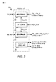
示されるように図2は本実施形態に従う図1の無線周波数(RF)トランシーバ(トランシーバ20)のブロック図である。トランシーバ20は、送信信号処理ブロック22、受信信号処理ブロック24、RFローカルオシレータ(RF LO)発生ブロック28、ならびに、コントロールおよびステータスブロック26を含む。コントロールおよびステータスブロック26は、ジャマー検出信号を含んでいるプロセッサ70に/から(to/from)デジタルコントロールロジックを提供する。RF LO発生ブロック28中に基準クロック発信器80からのREF_CLKが供給される。
As shown, FIG. 2 is a block diagram of the radio frequency (RF) transceiver (transceiver 20) of FIG. 1 according to the present embodiment. The
トランシーバ20は一つの送信および受信信号処理ブロックしか示されていないが、多数の(multiple)受信ブロック、多数の送信ブロックのいかなる組合せ、または、可能な送信および受信信号処理ブロック配置(configurations)のいかなる数でもって存在し得る。例えば、送信信号プロセッサブロック22および受信信処理号ブロック24は別の機能のブロックとして示されているが、ハーフデュープレックス(half duplex)無線デバイスモード内である程度は結合され(combined)得る。同様に、RF LO発生ブロック28は、送信信号処理ブロック22と受信信号処理ブロック24との間に配置された別の普通のブロックとして論理的には示されているが、他の配置(configurations)も考えられる。
示されるように図3は本実施形態に従う図2の無線周波数(RF)ローカルオシレータ(LO)発生ブロック28である。RF LO発生ブロック28は、RX LO発生ブロック29とTX LO発生器37とを含む。RX LO発生ブロック29は、RF PLLおよびループフィルタを具備するチャンネル選択チューニングブロック31を含む。チャンネル選択チューニングブロック31は、基準クロック発信器80からのREF_CLKを、RF VCO 33を所望の周波数にロックするためのRF VCO 33からの出力信号、RX_VCOと比べる。チャンネル選択チューニングブロック31からの出力、VtはRF VCO 33の出力信号RX_VCOの周波数をチューニングするためのアナログコントロール信号である。
As shown, FIG. 3 is the radio frequency (RF) local oscillator (LO)
出力信号RX_VCOはさらにLO発信ブロック35により処理され、そして、周波数は所望の受信RFチャンネル周波数、RX_LOに変換される。LO発信ブロック35は、さまざまな周波数多重または信号RX_VCOとRX_LOの分割比を作成するための周波数分割器、周波数ミキサ、スイッチ、または、全ての三つのタイプの要素の組合せを用いて実施され得る。RX_LO信号周波数は、特定の動作周波数バンド(USセルラ、US-PCS、IMT、GPSなど)内の所望のRX RFチャンネル周波数に等しい。RX_LO信号は図2の受信信号処理ブロック24に接続される。
The output signal RX_VCO is further processed by the LO transmit
TX LO発生器37に対しての等価ブロックは簡潔のために示されていない。LO発生ブロック29に対して示されたのと同様なブロックは、TX LO発生器37、ならびに、RXおよびTXの両方またはRXのみの多重信号処理ブロッに対して必要されるのと同じ数のLO発信ブロックに対して利用されることは容易に理解されるはずである。
The equivalent block for
示されるように図4は本実施形態に従う図3の無線周波数電圧制御発信器、RF VCO33の概略図である。RF VCO33は、出力信号RX_VCOの周波数をシフトするために二つのバラクタ要素41(VCAP1およびVCAP2)と並列な固定インダクタLvco43を含む。この周波数(ラジアン/秒で)は{1/(Lvco*Cvcap)}1/2に等しく、ここで、Cvcapは二つのバラクタ要素41(VCAP1およびVCAP2)のトータルのキャパシタンスである。周波数チューニングは、VCAP1およびVCAP2を横切る入力であるチャンネル選択チューニングブロック31からの出力、Vtを調整することでトータルのキャパシタンスを変えることで成し遂げられる。図3に示すように、RF VCO 33の出力、RX_VCOは、それから、もとのチャンネル選択チューニングブロック31へと、そして、LO発信ブロック35へと入力される。
As shown, FIG. 4 is a schematic diagram of the
図4に示された回路は、RXおよびTXの両方の多重パス(multiple paths)のために必要とされるのと同じ数のRF VCO(複数)を横切って適用し得る。また、一つのRF VCOは、多重周波数バンド内の同時動作が要求されない限りは、多重モードおよび動作バンドをカバーし得る。RF VCOの出力周波数をシフトできる他の回路トポロジーも知られているが、機能的には同等である。 The circuit shown in FIG. 4 may be applied across as many RF VCOs as are required for both RX and TX multiple paths. Also, one RF VCO can cover multiple modes and operating bands unless simultaneous operation within multiple frequency bands is required. Other circuit topologies that can shift the output frequency of an RF VCO are also known, but are functionally equivalent.
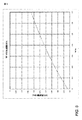
図5は本実施形態に従うRF VCO出力周波数対図4のチューニング電圧(Vt)のグラフの例証である。この例の設計では、RF VCO 33の周波数チューニングレンジは、0と.7ボルトDCとの間のチューニング電圧,Vtによって連続的に調整できる。Vtチューニングスロープ(Kv=MHz/V)および絶対周波数チューニングレンジは回路トポロジーおよび要素値を変えることで変更され得るが、機能的には同等である。
FIG. 5 is an illustration of a graph of RF VCO output frequency vs. tuning voltage (Vt) of FIG. 4 according to this embodiment. In this example design, the
図5から明らかのように、Vtチューニングスロープ(Kv=MHz/V)は非常に大きい(約KV=5,000MHz/V)。大きなVtチューニングスロープの結果として、RF VCO 33は、チューニング電圧,Vt上のノイズに敏感である。例えば、もし、2MHz(Fsw)で1uV(一ボルトの百万分の一)の正弦波リップルが0.2V DCチューニング電圧を連れたVt上に結合されると、RF VCO 33 出力は、2MHz毎に間隔をあけたスペクトル成分(スプリアス成分(spurious content))を連れた2.57GHzの基本周波数からなる。
As is apparent from FIG. 5, the Vt tuning slope (Kv = MHz / V) is very large (about KV = 5,000 MHz / V). As a result of the large Vt tuning slope, the
スプリアス成分の相対振幅(relative amplitude)は、RF VCO 33の周波数変調(FM)に対してのベッセル関数Jn(beta)を用いて計算され得れ、ここで、nはスイッチング電圧レギュレータ40に対してのスイッチャ周波数,Fswの調波インデックス(harmonic index)(1, 2, 3...)に等しく、そして、betaは変調インデックス(beta=Kv*ripple/Fsw)である。Kv=5000MHz/V、電圧リップル=1uV、および、Fsw=2MHzの値に対して、RF VCO 基本周波数から2MHzオフセットの第1のスペクトル・コンポーネント(n=1)は58dBcとなる。
The relative amplitude of the spurious component can be calculated using the Bessel function Jn (beta) for the frequency modulation (FM) of the
Vt上により多くの電圧リップルが結合すると、RF VCO 33 出力上で測定されるスプリアス成分の振幅も相対振幅において増大する。次に図7および8において示されるように、スプリアス成分は異なる動作条件下のトランシーバ20の無線特性(radio performance)を下げ得る。
As more voltage ripple couples on Vt, the amplitude of the spurious component measured on the
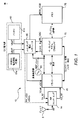
図6は、図1の好ましい実施形態に従うスイッチング電圧レギュレータ40の概略図である。スイッチング電圧レギュレータ40は、図1の電力源61bからの電圧源入力,VBATと、トランシーバ20に対しての電圧出力TCVR_VDDと、RFフロント-エンド14に対してのPA_VDDおよびVBIASと、プロセッサ70に対してのBB_VDDと、図1のメモリ75に対してのMEM_VDDを含む。図1のスイッチャ40またはプロセッサ70のいずれかに選択されたなら、代わりの入力電圧VEXTもまた使用され得る。PA_VDD、VBIAS、BB_VDDおよびMEM_VDDなどの個々の出力電圧は、異なる供給電圧が必要ならば、追加のスイッチング電圧レギュレータにより別々に発生させれても構わない。
FIG. 6 is a schematic diagram of a switching
スイッチング電圧レギュレータ40の入力と出力,VEXTとTCVR_VDD(PA_VDD、VBIAS、BB_VDDおよびMEM_VDDと一緒に)との間は、それぞれ、スイッチング電圧レギュレータ・コントローラ63、プログラマブル・クロック・ディバイダ(programmable clock divider)64、直列インダクタLsw65およびフィルタリング・キャパシタCsw67と一緒にスイッチ61aおよび61bである。
Between the input and output of the switching
スイッチング電圧レギュレータ・コントローラ63は、基準電圧発生器62の出力電圧に基づいて、出力電圧TCVR_VDD(PA_VDD、VBIAS、BB_VDDおよびMEM_VDDと一緒に)を、プログラマブル電圧セッティング値と比べ、そして、出力電圧,TCVR_VDD(PA_VDD、VBIAS、BB_VDDおよびMEM_VDDと一緒に)が、プログラマブル電圧セッティング値に収束するように、S1およびS2のディーティサイクルを調整する。プログラマブル電圧セッティング値は、プロセッサ70により設定され、または、スイッチング電圧レギュレータ40の内部で固定値となるハードウエア構成にすることができる。スイッチング電圧レギュレータ・コントローラ40へのスイッチャ周波数,Fswは、プログラマブル・クロック・ディバイダ64に対してのスイッチャ周波数セッティング値により設定される。
Based on the output voltage of the reference voltage generator 62, the switching
プログラマブル・クロック・ディバイダ64は、スイッチ61aおよび61bをコントロールするために用いられる、REF_CLK(この例では基準クロック発信器80からの)と、スイッチャ周波数,Fswとの間の整数周波数(integer frequency)ディバイダで構わない。一実施形態において、REF_CLK出力周波数は19.2MHzであり、そして、プログラマブル・クロック・ディバイダ64は、次に示す図9のプロセスに依存して異なる三つの周波数設定値(6,7,または8によって分割)の間に設定される。
Programmable clock divider 64 is an integer frequency divider between REF_CLK (from
スイッチング電圧レギュレータ40は、図1および6に示される供給電圧TCVR_VDDを介して直接的にトランシーバ20に結合される。スイッチング電圧レギュレータ40のスイッチャ周波数,Fswは、トランシーバ20のパフォーマンスに干渉し得る。干渉はTCVR_VDD上の電圧リップルとしてあらわれる。電圧リップルは離散的な周波数コンポーネントからなる。各周波数コンポーネントは、スイッチング電圧レギュレータ40のスイッチャ周波数,Fswの調波(harmonics)である。各調波のパワーレベルは、(i)スイッチング電圧レギュレータ40のスイッチャ周波数,Fswのディーティサイクル、(ii)出力電圧TCVR_VDDの容量的フィルタリング(capacitive filtering)の度合い、他に、(iii)TCVR_VDDとトランシーバ20内の敏感な回路(sensitive circuits)との間の結合の法方に依存する。
The switching
図5を参照して前に述べたように、ランシーバ20内の最も敏感な回路はRF VCO 33である。スイッチング電圧レギュレータ40のスイッチャ周波数,Fswの調波に等しい周波数オフセットで、RF VCO 33出力,RX_VCOの周波数変調(FM)を生成するために、スイッチング電圧レギュレータ40の出力での電圧リップルは、RF VCO 33のチューニング電圧,Vtにコンバインし得る。
As previously described with reference to FIG. 5, the most sensitive circuit in the
スイッチング電圧レギュレータ40のスイッチャ周波数,Fswは、(直接的に、または、RF VCO 33に結合されて)ある動作条件下の無線通信デバイス10のパフォーマンスに、干渉し得る。現在の好ましい実施形態に従う図1および図6に示されるスイッチング電圧レギュレータ40に対して動作しているスイッチャ周波数を調整的に選択するための技術が異なる動作条件に対して説明される。
The switcher frequency, Fsw, of the switching
スイッチング電圧レギュレータ40が図1の無線通信デバイス10の一部である場合、第1の動作条件は電流動作技術モード(current operating technology mode)(GSM(登録商標),CDMA,WCDMA等)に基づく。各技術モードは予め定められたRFチャンネルバンド幅(Fch)に関連されている。GSM(登録商標)に対しては、RFチャンネルバンド幅(Fch_gsm)は1.23MHzである。CDMAに対しては、RFチャンネルバンド幅(Fch_cdma)は1.23MHzである。WCDMAに対しては、RFチャンネルバンド幅(Fch_wcdma)は3.84MHzである、等である。
If the switching
ここでの一態様は、与えられた技術モードに関連されている、スイッチング電圧レギュレータ40のスイッチャ周波数,Fswは、RFチャンネルバンド幅の半分よりも大きくなるように調整される(Fsw>Fch/2)。このスイッチャ周波数調整は、トランシーバ20上のスイッチング電圧レギュレータ40干渉が、ベースバンドアナログ受信信号(図2のRX_I_FILTおよびRX_Q_FILT)および送信信号(図2のTX_I,TX_Q)上に現れることを低減または除去する。
One aspect here is that the switcher frequency, Fsw, of the switching
フルデュプレックスモード(full duplex mode)で動作している無線通信デバイス10の場合、スイッチング電圧レギュレータ40のスイッチャ周波数をRFチャンネルバンド幅の半分よりも大きく(Fsw>Fch/2)設定することは、特に干渉を緩和するのに役立つ。フル−デュプレックスモードの一例は、送信RFチャンネル(Ftxでの)と受信RFチャンネル(Frxでの)との間の周波数分離がDに等しく(D=Frx−Ftx)、そして、送信および受信RFチャンネルがともに同時にアクティブの場合である。Dは無線通信デバイス10と関連する動作周波数バンドに基づいて設定される。単一周波数バンドの無線通信デバイス10においては、RF動作バンドは、技術モード(USセルラ、US PCS、IMTバンド内のCDMAなど)に対して重要な一つの周波数バンドのみを含む。マルチ−周波数バンドの無線通信デバイス10(例えば、USセルラ、US PCSおよび/またはCDMA(IMT)能力)においては、動作周波数バンドは、いくつかの可能な周波数バンドの一つである。USセルラに対して、D=45MHz、US PCSに対して、D=80MHzである。IMTバンド内のCDMAに対して、D=190MHzである、等である。
In the case of the
理想的な状況では、送信RFチャンネル(Ftxでの)はスプリアス成分(スイッチング電圧レギュレータ40からの)とミックスしてはならない、それは受信RFチャンネル周波数で(Frxで)干渉を生成する可能性があるからである。スイッチング電圧レギュレータ40のスイッチャ周波数,Fswは、実際は、D−Fch<N*Fsw<D+Fchとなるような周波数の範囲内に入ってはならない、ここでN*FswはDに最も近い整数スイッチャ周波数調波(integer switcher frequency harmonic)の周波数の範囲である。ここでの態様に従いスイッチャ周波数を選択することにより、スイッチング電圧レギュレータ40から送信RFチャンネルおよび受信RFチャンネルのどちらの上への干渉は緩和される。
In an ideal situation, the transmit RF channel (at Ftx) should not mix with the spurious component (from switching voltage regulator 40), which can generate interference (at Frx) at the receive RF channel frequency. Because. The switcher frequency, Fsw, of the switching
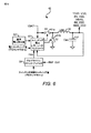
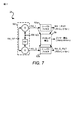
示されるように図7は本実施形態に従う図2の受信信号処理ブロック24のブロック図である。受信信号処理ブロック24は、RX RF I/Qダウンコンバータ55、一対のベースバンドアナログローパスフィルタ57aおよび57b、ならびに、ジャミング検出ブロック59を含む。代わりの実施形態は、低ノイズ増幅器、RFフィルタリング、多重RFバンド、および、種々の形態のコントロール回路を含み得る。
As shown, FIG. 7 is a block diagram of the received
I/Qダウンコンバータ55内のダイレクト変換(RFからベースバンド)ミキサを用いて受信RF信号をダウンコンバートする前のRXバンド外の干渉と同様に、(図1の)RFフロント-エンド14からのRX_RF信号は、I/Qダウンコンバータ55中に供給される。(トランシーバ20またはプロセッサ70上で)アナログで、または、(トランシーバ20またはプロセッサ70上でのアナログ−デジタル・コンバータを伴う変換後の)デジタル領域(digital domain)でさらに処理する前に、I/Qダウンコンバータ55の出力,RX_IおよびRX_Qは、ローパスフィルタ57aおよび57bによってフィルタされる。図7には示されていないが、ローパスフィルタ57aおよび57bは、プロセッサ70内でのアナログ−デジタル変換の前に、RX_I_FILTおよびRX_Q_FILTの振幅を調整するための、固定または可変のゲインを含んでも構わない。
Similar to interference outside the RX band before downconverting the received RF signal using a direct conversion (RF to baseband) mixer within the I /
ジャミング検出ブロック59はジャマー検出信号を送り、選択された受信信号からの周波数オフセットであるジャマーが現れた時に、その値はプロセッサ70に伝達する。ジャミング検出ブロック59は、RX_I_FILTおよびRX_Q_FILTからのオフセットのジャマーの出現を周波数内で検出するために、アナログローパスフィルタ57aおよび/または57bの前または後で、ベースバンドアナログ領域(baseband analog domain)内で測定を行っても構わない。代わりに、ジャミング検出ブロック59は、プロセッサ70内でデジタル領域内で実行されても構わなく、または、トランシーバ20とプロセッサ70との間で分けられても構わない。
The jamming detection block 59 sends a jammer detection signal, and when a jammer that is a frequency offset from the selected received signal appears, the value is transmitted to the
所望の受信RFチャンネルからの一つまたは二つの異なる周波数オフセットでのRX_RF信号経路内での一つまたは二つのジャマーの出現は、(図2−4の)RX_VCOおよびRF_LO信号上に現れるスプリアス成分とミックスされた時に、所望のRFチャンネルと干渉し得る。この望まないミキシングプロダクト(mixing product)は、ベースバンド受信信号経路(図7のRX_I,RX_Q,RX_I_FILTおよびRX_Q_FILT)で測定された受信信号バンド幅内に入り得る。 The appearance of one or two jammers in the RX_RF signal path at one or two different frequency offsets from the desired received RF channel is the spurious component appearing on the RX_VCO and RF_LO signals (FIGS. 2-4). When mixed, it can interfere with the desired RF channel. This unwanted mixing product may fall within the received signal bandwidth measured in the baseband received signal path (RX_I, RX_Q, RX_I_FILT and RX_Q_FILT in FIG. 7).
ここでの他の態様において、スイッチング電圧レギュレータ40のスイッチャ周波数は、ベースバンド受信信号経路内に一つまたは複数のジャマーが所定よりも上そして検出可能なしきい値で現れた時に、ベースバンド受信信号経路中のこの干渉を、緩和するように設定される。受信信号処理ブロック24に作用している図2および図8に関連した上述のスプリアス成分問題はグラフィカルに例証することが可能である。
In another aspect herein, the switcher frequency of the switching
示されるように図8は、図1−7のジャマーの存在下における、(i)RF_LO出力、(ii)送信RFチャネル漏れ、および(iii)レシーバ特性に対しての、スイッチング電圧レギュレータからの干渉の影響を示している、グラフィカルな例証である。例証90は(図7の)I/Qダウンコンバータ55への入力としての、Frxで受信信号、Ftxで送信信号漏れ、および、(図7のブロック35からの)Fj1でジャマー信号を持った増幅された/フィルタされたRX_RF信号入力を含む。例証90はまた(図7の)I/Qダウンコンバータ55への第2の入力としての、N*Fsw(ここでN=−2,−1,+1,+2,+3および+4)に対応する周波数オフセットにスイッチャ周波数スプリアス成分を持った(図3のブロック35からの)RX_LO信号を含む。例証90はまた同相(the in-phase)または図7のI/Qのダウンコンバータ55のIダウンコンバータからのRX_I信号を含む。
As shown, FIG. 8 shows interference from a switching voltage regulator for (i) RF_LO output, (ii) transmit RF channel leakage, and (iii) receiver characteristics in the presence of the jammer of FIGS. 1-7. This is a graphical illustration showing the impact of Example 90 is an amplification with the received signal at Frx, the transmitted signal leakage at Ftx, and the jammer signal at Fj1 (from
例証されたRX_I信号は、I/Qダウンコンバータ55ベースバンド出力でのLO RX_RFおよびRX_LO入力信号のミキシングプロダクト(mixing product)を示している。所望の受信ベースバンドチャンネル、RX_I信号経路中のRX_BBはDCで集中される(centered)。RX_BB信号バンド幅より上の周波数で、J1周波数でのジャマーに対してのオフセット(offsets)にてスペクトル・コンポーネント(spectral components)があり、および、Dtx周波数にてTX信号漏れがある。加えて、受信チャンネル、RX_BB、特に、J1−3*FswおよびDtx−N*Fs(ここでNは整数、N*Fsはスイッチング電圧レギュレータ40のスイッチャ周波数の調波(harmonic))内に入るスプリアス成分がある。受信チャンネルハンド幅内のスプリアス成分は、RX_BB信号を変調する前は、フィルタまたは除去することができず、そして、プロセッサ70による適切なRX_BB復調と干渉する。
The illustrated RX_I signal shows the mixing product of the LO RX_RF and RX_LO input signals at the I /
TXおよびRX周波数の間の周波数バンドオフセットに依存して、スイッチング電圧レギュレータ40のスイッチャ周波数(Fsw)およびオフセットジャマー周波数(この例ではJ1)は、I/Qダウンコンバータ55(RX_IまたはRX_Q)のベースバンド出力にて測定されるように受信信号処理干渉の多重のソース(multiple source)があり得る。以下にさらに詳細に説明するように、スイッチング電圧レギュレータ40のスイッチャ周波数,Fswを調整することにより、受信信号処理干渉は異なる動作条件に対して最小化され得る。
Depending on the frequency band offset between the TX and RX frequencies, the switcher frequency (Fsw) and offset jammer frequency (J1 in this example) of the switching
図9は、好ましい実施形態に従うスイッチング電圧レギュレータコントローラを利用したスイッチング電圧レギュレータのためのスイッチャ周波数を選択するプロセスの動作フロー図である。動作フロー図100は、現在の動作条件(例えば、現在の動作バンド、動作モードおよび/またはジャマー検出値)を特定するプロセッサ70から始まる(ブロック101)。プロセッサ70はそれから現在の動作条件に基づいてスイッチャ周波数セッティング値を生成する(ブロック103)。プログラマブル・クロック・ディバイダ64は、基準周波数クロック信号,REF_CLKと一緒にスイッチャ周波数セッティング値を受け取りそして処理して、所望のスイッチング周波数を発生する(ブロック105)。スイッチング電圧レギュレータ・コントローラ63は、スイッチ信号を発生するために、プログラマブル・クロック・ディバイダ64からスイッチング周波数、例えばプロセッサ70から電圧セッティング値、および、基準電圧発生器62から信号を受け取る(ブロック107)。スイッチ信号は、スイッチング電圧レギュレータ40の出力電圧を調整する効果を有するスイッチ(61a,61b)を切り替える(toggle)ために用いられる(ブロック109)。現在の動作条件が変化したなら、いつでも、動作フロー図100はリスタートしても構わない(ブロック101に戻る)。マルチバンドCDMA無線通信デバイスに対してのより具体的な動作フロー図を以下にさらに説明する。
FIG. 9 is an operational flow diagram of a process for selecting a switcher frequency for a switching voltage regulator utilizing a switching voltage regulator controller according to a preferred embodiment. The operational flow diagram 100 begins with the
図10は、好ましい実施形態に従うCDMAモードに対しての異なる動作周波数バンド内におけるスイッチング電圧レギュレータのための最適なスイッチャ周波数,Fswを選択するプロセスの動作フロー図である。動作フロー図200はスタートブロック(ブロック201)から始まり、その後、使用される特別な動作バンドのためのトランシーバ20内の一つまたは複数のレジスタをプログラミングすることが続く(ブロック203)。いったん動作バンドが決定されると、スイッチング電圧レギュレータ40のスイッチャ周波数(Fsw)が2.4MHz(CDMA PCSバンド)、2.74MHz(CDMA450/800バンド)または3.2MHz(CDMA IMTバンド)に等しくなるように、19.2MHzの基準クロック周波数信号,REF_CLKに基づいて、スイッチング電圧レギュレータ40内の、プログラマブル・クロック・ディバイダ64は、異なる三つの値6,7または8の一つに設定される(ブロック205)。
FIG. 10 is an operational flow diagram of a process for selecting the optimal switcher frequency, Fsw, for the switching voltage regulator in different operating frequency bands for the CDMA mode according to the preferred embodiment. The operational flow diagram 200 begins with a start block (block 201) followed by programming one or more registers in the
スイッチャ周波数,Fswは、複数(multiple)のパラメータに基づき計算される。第1の基準(criterion)は所望のチャンネルバンド幅(CDMAに対してFch=1.23MHz)である。図1、2、7、および8に示されるように、スイッチングノイズがベースバンドI/Oアナログ信号中に直接的に結合しないことを保証するために、Fswは、Fchの半分よりも大きくなければならない。下の表1は動作モードに対するFchを示す。追加の動作モードが含まれていても構わない。動作フロー図200は一つの動作モード、CDMAに簡略化されている。レシーバ入力に現れる送信信号漏れおよび/またはジャミングトーン(jamming tones)があるとき、スイッチャ周波数,Fswはより高い値に調整されるという追加の基準を必要とするであろう。

第2の基準は(CDMA等のフルデュプレックスシステムにおける)送信RFチャネル漏れが受信RFチャンネルをそこなわない(not corrupt)ことである。前述したように、RF LO発生ブロック28はスイッチャ周波数電圧リップルに汚染され、そして、スイッチング電圧レギュレータ40からの調波周波数(harmonic frequencies)に対応している。もし、スイッチャ周波数調波(switcher frequency harmonic)が送信RFおよび受信RFチャネル間の周波数分離に近い周波数オフセットであると、特定のスイッチャ調波は、(スイッチャ周波数電圧リップルがRF VCO33(RX_VCOおよびRX_LO信号)中に結合した後)I/Qダウンコンバータ55での送信RFチャネル漏れとミックスし、そして、受信信号処理干渉(receive signal processing interference)を発生させるであろう。同様に、スイッチャ周波数電圧リップルおよび対応する調波周波数はTX LO発生器37内のRF VCOに結合することができ、そして、トランシーバ20の送信信号処理ブロック22の出力内にスプリアス成分を生成することができる。この送信スプリアス成分は受信RFチャネル内に入ることができ、そして、受信RFチャネル干渉を生成することができる。
The second criterion is that transmit RF channel leakage (in a full duplex system such as CDMA) does not corrupt the received RF channel. As described above, the RF
異なる動作バンドに対してRFチャネル分離を送るための受信RFチャネルを以下の表2に示す。Fswが方方程式ここでは|N*Fsw−D|>Fch/2(ここでNは整数)を保証することにより、図7−8に示されるように、スイッチャ周波数調波は受信ベースバンドI/Qアナログ信号,RX_Iおよび/またはRX_Q中に直接的に結合しなくなるはずである。
第3の指針は、所望の受信RFチャネルと周波数が近いジャミング干渉の存在に基づく。(RF VCO33上に結合された)基本のスイッチャ周波数は、ベースバンドチャンネルバンド幅(図8のRX_BB)内に干渉を生成するために、フィルタで除去(filter out)または削除(eliminate)できないオフセットジャミングトーン(RFでFJ1、図8のベースバンドでJ1)とミックスすることができる。異なる動作バンドおよびモードに対する受信信号処理ブロック24ジャミング仕様は、公になった最小特性基準(published minimum performance standards)に応じるように適用し得る。CDMAの場合、所望のRX RFチャンネルからのジャマー周波数オフセット(シングルトーンテストに対してはJ1オフセットまたはツートンテストに対してはJ1+J2オフセット)は、以下の各周波数バンドにつき以下の表3のように明示される。
受信信号処理ブロック24が(図7の)ジャミング検出回路59を有するとすると、スイッチャ周波数はFsw>(J1またはJ2)+Fch/2となるように調整され得る。許可された最大スイッチャ周波数に依存して、J1またはJ2周波数オフセットは、上記のFsw式に対して表3から選ばれ得る。第2または第3の指針の両方を満足するスイッチャ周波数がなければ、ジャミング干渉の存在はTX信号漏れ(第2の指針)に優先する。
If the received
19.2MHzのクロック周波数信号,REF_CLKが(図6の)プログラマブル・クロック・ディバイダ64に入力されるとして前記三つの制約を適用すると、表4に示されるように、CDMAにおける多重の(multiple)動作条件に対して、最適なスイッチャ周波数,Fswは計算され得れ、そして、格納され得る。2.4MHzは19.2MHzを8で割ることにより、2.74MHzは19.2MHzを7で割ることにより、そして、3.2MHzは19.2MHzを6で割ることにより発生させられる。一実施形態では、6,7,および8のスイッチャ周波数値は、ジャマーの有りおよび無しの異なるCDMA周波数バンドに対して選択される。
ひとたびFswがプログラムされると、ジャミング検出回路59は、ポールされる(polled)か、または、干渉(ブロック107)として用いられるかのどちらかである。 Once Fsw is programmed, the jamming detection circuit 59 is either polled or used as interference (block 107).
(表4に従う)CDMA−PCSモードにおいてジャマー検出信号がアクティブ(高ロジックレベル)のとき、スイッチャ周波数を8から7に変えることにより、スイッチャ周波数(Fsw)は2.4Hzから2.74Hz(ブロック109)に変えられる。ひとたびジャマーがもはや現れなくなると、ジャマー検出は、低ロジックレベルに遷移し、そして、スイッチャ周波数を8に変えることにより(ブロック105が繰り返される)、スイッチャ周波数(Fsw)は2.4MHzに戻り、そして、ジャミング検出回路59はモニタリングを続ける(ブロック107等)。利用できる基準信号周波数信号,REF_CLK、および、前記三つの基準が最適に満たされるようなプログラマブル・クロック・ディバイダ64に対してのディバイダ比(divider ratios)に依存して、他のスイッチャ周波数は用いられ得る。 When the jammer detection signal is active (high logic level) in CDMA-PCS mode (according to Table 4), the switcher frequency (Fsw) is changed from 2.4 Hz to 2.74 Hz (block 109) by changing the switcher frequency from 8 to 7. ). Once the jammer no longer appears, jammer detection transitions to a low logic level, and by changing the switcher frequency to 8 (block 105 is repeated), the switcher frequency (Fsw) returns to 2.4 MHz, and The jamming detection circuit 59 continues monitoring (block 107 etc.). Depending on the available reference signal frequency signal, REF_CLK, and divider ratios for the programmable clock divider 64 such that the three criteria are optimally met, other switcher frequencies are used. obtain.
信号は、さまざまな異なる技術の任意のものを用いて表され得ることが、当業者に理解されるであろう。例えば、上記記載を全体にわたって言及されるデータ、命令(instructions)は、電圧、電流、電磁波、磁界または光粒子、またはこれらを組み合わせたものによって表され得る。 Those skilled in the art will appreciate that the signal may be represented using any of a variety of different technologies. For example, data, instructions referred to throughout the above description may be represented by voltage, current, electromagnetic waves, magnetic fields or light particles, or a combination thereof.
本書類内の開示に関連して説明されたさまざまな例示的な無線周波数またはアナログ回路ブロックは、本開示で述べられたのと同じ機能を実行するともに、ロジック回路およびシステムと分離または組み合わせられた、さまざまな異なる回路トポロジー、一つまたは複数の集積回路にて実行され得ることが、当業者にさらに理解されるであろう。 The various exemplary radio frequency or analog circuit blocks described in connection with the disclosure within this document perform the same functions described in this disclosure, and are separated or combined with logic circuits and systems. It will be further appreciated by those skilled in the art that it can be implemented in a variety of different circuit topologies, one or more integrated circuits.
本書類内の開示に関連して説明されたさまざまな例示的な論理的なブロック、モジュール、回路およびアルゴリズムステップは、電子的なハードウェア、コンピュータソフトウェア、またはこれらの組み合わせとして実行され得ることが、当業者にさらに理解されるであろう。このハードウェアとソフトウェアとの互換性(interchangeability)を明確に示すために、種々の例示的なコンポーネント、ブロック、モジュール、回路、およびステップは、全般的にそれらの機能性の観点から、上記では説明してきた。そのような機能性がハードウェアで実行されるかソフトウェアで実行されるかは、特定のアプリケーションおよび全体のシステムに課せられた設計の制約に依存する。当業者は、前記記載された機能性を、各特定のアプリケーションにつき種々の方法で実行し得り、しかし、そのような実行の決定は、本開示の範囲からの逸脱を生じさるものとして解釈されるべきではない。 Various exemplary logical blocks, modules, circuits, and algorithm steps described in connection with the disclosure within this document may be implemented as electronic hardware, computer software, or a combination thereof. It will be further understood by those skilled in the art. To clearly illustrate this hardware and software interchangeability, various illustrative components, blocks, modules, circuits, and steps are generally described above in terms of their functionality. I have done it. Whether such functionality is implemented as hardware or software depends upon the particular application and design constraints imposed on the overall system. Those skilled in the art can implement the described functionality in a variety of ways for each particular application, but such implementation decisions are interpreted as causing deviations from the scope of this disclosure. Should not.
本書類内の開示に関連して述べられたさまざまな例示的な論理的なブロック、モジュール、および回路は、本書類内に述べられた機能を実行するように設計された汎用プロセッサ、デジタルシグナルプロセッサ(DSP)、特定用途向け集積回路(ASIC)、フィールドプログラマブルゲートアレイシグナル(FPGA)、またはその他のプログラマブル論理デバイス、ディスクリートゲートまたはトランジスタロジック、ディスクリートハードウェア部品、またはこれらを組み合わせたものによって、実装または実行され得る。汎用プロセッサは、マイクロプロセッサであっても良いが、代わりに前記プロセッサは従来のプロセッサ、コントローラ、マイクロコントローラ、またはステートマシンのいずれであっても構わない。プロセッサはまた、コンピューティングデバイスを組み合わせたものとして実装されても構わなく、例えば、DSPとマイクロプロセッサ、複数のマイクロプロセッサ、DSPコアと接続された一つ以上のマイクロプロセッサ、またはその他のそのような構成を組み合わせたものである。 The various exemplary logical blocks, modules, and circuits described in connection with the disclosure in this document are general purpose processors, digital signal processors designed to perform the functions described in this document. Implemented by (DSP), application specific integrated circuit (ASIC), field programmable gate array signal (FPGA), or other programmable logic device, discrete gate or transistor logic, discrete hardware components, or combinations thereof Can be executed. A general purpose processor may be a microprocessor, but in the alternative, the processor may be any conventional processor, controller, microcontroller, or state machine. A processor may also be implemented as a combination of computing devices, such as a DSP and a microprocessor, a plurality of microprocessors, one or more microprocessors connected to a DSP core, or other such It is a combination of configurations.
本書類内の開示に関連して述べられた方法またはアルゴリズムのステップは、ハードウェア、プロセッサによって実行されるソフトウェアモジュール、またはこれら2つを組み合わせたものによって、直接的に具体化され得る。ソフトウェアモジュールは、RAMメモリ、フラッシュメモリ、ROMメモリ、EPROMメモリ、EEPROMメモリ、レジスタ、ハードディスク、取外し可能ディスク、CD−ROM、または当技術分野で知られている任意の他の形態の記憶媒体内に存在してもよい。例示的な記憶媒体は、プロセッサが、記憶媒体から情報を読み出し、記憶媒体に情報を書き込むことができるようにプロセッサに結合されている。代替法では、記憶媒体は、プロセッサと一体であってよい。プロセッサおよび記憶媒体は、ASIC内に存在してもよい。ASICはユーザー端末内に存在してもよい。代替法では、プロセッサおよび記憶媒体は、ユーザー端末内でディスクリートコンポーネントとして存在してもよい。 The method or algorithm steps described in connection with the disclosure within this document may be directly embodied by hardware, software modules executed by a processor, or a combination of the two. The software modules are in RAM memory, flash memory, ROM memory, EPROM memory, EEPROM memory, registers, hard disk, removable disk, CD-ROM, or any other form of storage medium known in the art. May be present. An exemplary storage medium is coupled to the processor such that the processor can read information from, and write information to, the storage medium. In the alternative, the storage medium may be integral to the processor. The processor and storage medium may reside in an ASIC. The ASIC may be present in the user terminal. In the alternative, the processor and the storage medium may reside as discrete components in a user terminal.
本開示の先の説明は、任意の当業者が本開示を作製かまたは使用することを可能にするために提供されている。本開示に対する種々の変更は、当業者に容易に明らかになり、そして、本書類で規定される一般的な原理は、本開示の範囲から逸脱することなく、他の変更に適用されてもよい。したがって、本開示は、本書類で説明された例および設計に限定されることを意図されるのではなく、本書類に開示される原理および新規な特徴に一致する最も広い範囲に一致することを意図される。 The previous description of the disclosure is provided to enable any person skilled in the art to make or use the disclosure. Various modifications to the present disclosure will be readily apparent to those skilled in the art, and the generic principles defined in this document may be applied to other modifications without departing from the scope of the present disclosure. . Accordingly, this disclosure is not intended to be limited to the examples and designs described in this document, but is to be accorded the widest scope consistent with the principles and novel features disclosed in this document. Intended.
Claims (27)
スイッチャ周波数を生成するために、基準クロック周波数信号と、少なくとも電流動作状態(current operating condition)を表すスイッチャ周波数セッティング値(switcher frequency setting value)とに応答するプログラマブル・クロック・ディバイダ(programmable clock divider)、および
前記出力電圧を調整する(regulate)ための、前記スイッチャ周波数と基準電圧とに応答するスイッチング電圧レギュレータ・コントローラ(switching voltage regulator controller)
を具備するデバイス。 A device including a switching voltage regulator for generating an output voltage,
A programmable clock divider responsive to a reference clock frequency signal and at least a switcher frequency setting value representing a current operating condition to generate a switcher frequency; And a switching voltage regulator controller responsive to the switcher frequency and a reference voltage to regulate the output voltage
A device comprising:
スイッチャ周波数を生成するために、基準クロック周波数信号と、少なくとも電流動作状態(current operating condition)を表すスイッチャ周波数セッティング値(switcher frequency setting value)とに応答する、プログラマブル・クロック・ディバイダ(programmable clock divider)、および
前記出力電圧を調整する(regulate)ための、前記スイッチャ周波数と基準電圧とに応答するスイッチング電圧レギュレータ・コントローラ(switching voltage regulator controller)
を具備するIC。 An integrated circuit (IC) for generating an output voltage for a switching voltage regulator comprising:
A programmable clock divider responsive to a reference clock frequency signal and at least a switcher frequency setting value representing a current operating condition to generate a switcher frequency And a switching voltage regulator controller responsive to the switcher frequency and a reference voltage for regulating the output voltage
IC comprising:
スイッチャ周波数を生成するために、基準クロック周波数信号と、少なくとも電流動作状態(current operating condition)を表すスイッチャ周波数セッティング値(switcher frequency setting value)とに応答する手段、および
前記出力電圧を調整する(regulate)ための、前記スイッチャ周波数と基準電圧とに応答する手段
を具備するデバイス。 A device for generating an output voltage for a switching voltage regulator comprising:
Means for responding to a reference clock frequency signal and at least a switcher frequency setting value representative of a current operating condition to generate a switcher frequency, and to regulate the output voltage And a means for responding to the switcher frequency and a reference voltage.
電流動作状態(current operating condition)を特定すること(identifying)、
前記電流動作状態に基づいてスイッチャ周波数セッティング値を生成すること、
プログラマブル・クロック・ディバイダ(programmable clock divider)を用い、前記スイッチャ周波数セッティング値と基準クロック周波数信号とを用いるスイッチャ周波数を生成すること、
少なくとも前記スイッチャ周波数に基づき、スイッチング電圧レギュレータ・コントローラ(switching voltage regulator controller)を用いて、スイッチ信号を生成すること、および
前記出力電圧を調整するために前記スイッチング電圧レギュレータの前記出力に結合されたスイッチをオンおよびオフに切り替えること(toggling)
を具備する方法。 A method of regulating the output voltage of a switching voltage regulator,
Identifying the current operating condition (identifying),
Generating a switcher frequency setting value based on the current operating state;
Generating a switcher frequency using the switcher frequency setting value and a reference clock frequency signal using a programmable clock divider;
Generating a switch signal using a switching voltage regulator controller based at least on the switcher frequency, and a switch coupled to the output of the switching voltage regulator to regulate the output voltage Toggling on and off (toggling)
A method comprising:
前記ジャミング検出回路からジャマー検出信号を受け取るための手段、および
前記スイッチング電圧レギュレータへの動作スイッチング周波数(operating switching frequency)に関連したスイッチャ周波数セッティング値(switcher frequency setting value)を生成するための、前記ジャマー検出信号に応答する手段
を具備するプロセッサ。 A processor configured to operate with a jamming detection circuit and a switching voltage regulator comprising:
Means for receiving a jammer detection signal from said jamming detection circuit; and said jammer for generating a switcher frequency setting value associated with an operating switching frequency to said switching voltage regulator A processor comprising means for responding to the detection signal.
前記ジャマー検出回路からジャマー検出信号を受け取らせ、および
前記ジャマー検出値および前記電流動作状態に応じて、前記スイッチング電圧レギュレータに関連した出力電圧を調整するための、前記スイッチング電圧レギュレータによる使用のためのスイッチャ周波数セッティング値を生成させるための命令(instructions)を持つコンピュータ読取り可能媒体を含むコンピュータプログラムプロダクト。 For a processor configured to operate with a jammer detection circuit and a switching voltage regulator,
For use by the switching voltage regulator to receive a jammer detection signal from the jammer detection circuit and to adjust an output voltage associated with the switching voltage regulator in response to the jammer detection value and the current operating state. A computer program product comprising a computer readable medium having instructions for generating switcher frequency setting values.
Applications Claiming Priority (3)
| Application Number | Priority Date | Filing Date | Title |
|---|---|---|---|
| US12/327,990 US8294445B2 (en) | 2008-12-04 | 2008-12-04 | Switching voltage regulator with frequency selection |
| US12/327,990 | 2008-12-04 | ||
| PCT/US2009/066882 WO2010065934A1 (en) | 2008-12-04 | 2009-12-04 | Switching voltage regulator with frequency selection |
Related Child Applications (1)
| Application Number | Title | Priority Date | Filing Date |
|---|---|---|---|
| JP2013253675A Division JP5805738B2 (en) | 2008-12-04 | 2013-12-06 | Switching voltage regulator with frequency selection |
Publications (1)
| Publication Number | Publication Date |
|---|---|
| JP2012511285A true JP2012511285A (en) | 2012-05-17 |
Family
ID=41718273
Family Applications (2)
| Application Number | Title | Priority Date | Filing Date |
|---|---|---|---|
| JP2011539765A Pending JP2012511285A (en) | 2008-12-04 | 2009-12-04 | Switching voltage regulator with frequency selection |
| JP2013253675A Active JP5805738B2 (en) | 2008-12-04 | 2013-12-06 | Switching voltage regulator with frequency selection |
Family Applications After (1)
| Application Number | Title | Priority Date | Filing Date |
|---|---|---|---|
| JP2013253675A Active JP5805738B2 (en) | 2008-12-04 | 2013-12-06 | Switching voltage regulator with frequency selection |
Country Status (8)
| Country | Link |
|---|---|
| US (1) | US8294445B2 (en) |
| EP (2) | EP2827505B1 (en) |
| JP (2) | JP2012511285A (en) |
| KR (1) | KR101263814B1 (en) |
| CN (2) | CN103997211B (en) |
| IN (1) | IN2014CN04321A (en) |
| TW (2) | TWI533627B (en) |
| WO (1) | WO2010065934A1 (en) |
Cited By (1)
| Publication number | Priority date | Publication date | Assignee | Title |
|---|---|---|---|---|
| JP2017063348A (en) * | 2015-09-25 | 2017-03-30 | ルネサスエレクトロニクス株式会社 | Radio communication device and radio communication method |
Families Citing this family (22)
| Publication number | Priority date | Publication date | Assignee | Title |
|---|---|---|---|---|
| DE102007046341A1 (en) * | 2007-09-27 | 2009-04-23 | Infineon Technologies Ag | Circuit arrangement for processing a high-frequency signal |
| EP2583377A1 (en) | 2010-06-21 | 2013-04-24 | Telefonaktiebolaget LM Ericsson (publ) | A coordinated power converter system |
| US20120154958A1 (en) * | 2010-12-20 | 2012-06-21 | Nexergy, Inc. | Use of a jfet as a failsafe shutdown controller |
| US8963527B2 (en) * | 2010-12-31 | 2015-02-24 | Integrated Device Technology Inc. | EMI mitigation of power converters by modulation of switch control signals |
| FR2992073B1 (en) * | 2012-06-19 | 2014-07-11 | Commissariat Energie Atomique | DEVICE FOR SUPPLYING AN ELECTRONIC CIRCUIT |
| US9003209B2 (en) * | 2012-06-29 | 2015-04-07 | Intel Corporation | Efficient integrated switching voltage regulator comprising switches coupled to bridge drivers to provide regulated power supply to power domains |
| US8975887B2 (en) | 2012-07-08 | 2015-03-10 | R2 Semiconductor, Inc. | Suppressing oscillations in an output of a switched power converter |
| US9014637B1 (en) * | 2013-09-27 | 2015-04-21 | Intel Corporation | Dynamic switching frequency control of an on-chip or integrated voltage regulator |
| US10439491B2 (en) * | 2014-02-14 | 2019-10-08 | Telefonaktiebolaget Lm Ericsson (Publ) | Power supply electronic circuit with IBC to control current ripple |
| TWI551070B (en) | 2015-05-08 | 2016-09-21 | 和碩聯合科技股份有限公司 | Portable electronic device |
| TWI609572B (en) * | 2015-05-15 | 2017-12-21 | 絡達科技股份有限公司 | Control method of rf switching module |
| CN107690753B (en) | 2015-05-29 | 2020-07-14 | 马克西姆综合产品公司 | Low power ultra-wideband transmitter |
| US9898218B2 (en) | 2016-02-05 | 2018-02-20 | International Business Machines Corporation | Memory system with switchable operating bands |
| EP3229357B1 (en) * | 2016-04-08 | 2020-08-19 | Nxp B.V. | Charge pump with reference voltage modification for avoiding specific frequencies |
| CN105978326B (en) * | 2016-06-20 | 2018-07-03 | 浙江大学 | DC-DC power source built in the optical fibre gyro that switching frequency is adjusted in real time |
| DE102016212656B4 (en) * | 2016-07-12 | 2019-05-29 | Hanon Systems | Control device for an electric compressor |
| US9923520B1 (en) | 2016-09-21 | 2018-03-20 | Qualcomm Incorporated | Switching power supply for RF power amplifiers |
| TWI607623B (en) * | 2016-10-07 | 2017-12-01 | 新唐科技股份有限公司 | Switched-capacitor dc-dc power converter and control method thereof |
| US10218366B1 (en) | 2017-11-27 | 2019-02-26 | Linear Technology Holding Llc | Phase locked loop calibration for synchronizing non-constant frequency switching regulators |
| CN108539973B (en) * | 2018-05-18 | 2019-12-31 | 深圳市华星光电技术有限公司 | TFT-LCD display, driving circuit thereof and switching power supply |
| CN112469112B (en) * | 2020-11-25 | 2023-03-21 | Oppo(重庆)智能科技有限公司 | Frequency control method, device, radio frequency system and communication equipment |
| CN114978229A (en) * | 2022-06-28 | 2022-08-30 | 维沃移动通信有限公司 | Radio frequency control method and device and electronic equipment |
Citations (2)
| Publication number | Priority date | Publication date | Assignee | Title |
|---|---|---|---|---|
| JPH05315980A (en) * | 1992-05-08 | 1993-11-26 | Victor Co Of Japan Ltd | Radio receiver |
| JP2007208718A (en) * | 2006-02-02 | 2007-08-16 | Kenwood Corp | Switching power supply |
Family Cites Families (30)
| Publication number | Priority date | Publication date | Assignee | Title |
|---|---|---|---|---|
| US4580107A (en) * | 1984-06-06 | 1986-04-01 | The United States Of America As Represented By The Secretary Of The Air Force | Phase lock acquisition system having FLL for coarse tuning and PLL for fine tuning |
| US4870699A (en) * | 1986-03-26 | 1989-09-26 | General Electric Company | Method and apparatus for controlling the frequency of operation and at least one further variable operating parameter of a radio communications device |
| US4879758A (en) * | 1987-01-02 | 1989-11-07 | Motorola, Inc. | Communication receiver system having a decoder operating at variable frequencies |
| US5150361A (en) * | 1989-01-23 | 1992-09-22 | Motorola, Inc. | Energy saving protocol for a TDM radio |
| US5363419A (en) * | 1992-04-24 | 1994-11-08 | Advanced Micro Devices, Inc. | Dual phase-locked-loop having forced mid range fine control zero at handover |
| JPH0870258A (en) * | 1994-09-30 | 1996-03-12 | Matsushita Electric Ind Co Ltd | Radio equipment |
| US5773966A (en) * | 1995-11-06 | 1998-06-30 | General Electric Company | Dual-mode, high-efficiency dc-dc converter useful for portable battery-operated equipment |
| JPH11332230A (en) | 1998-05-07 | 1999-11-30 | Alinco Inc | Switching power supply |
| US6204649B1 (en) | 2000-03-16 | 2001-03-20 | Micrel Incorporated | PWM regulator with varying operating frequency for reduced EMI |
| TW519792B (en) | 2000-08-30 | 2003-02-01 | Cirrus Logic Inc | Circuits and methods for reducing interference from switched mode circuits |
| US7058374B2 (en) | 2002-10-15 | 2006-06-06 | Skyworks Solutions, Inc. | Low noise switching voltage regulator |
| US7130602B2 (en) | 2002-10-31 | 2006-10-31 | Qualcomm Incorporated | Dynamically programmable receiver |
| US20040090802A1 (en) | 2002-11-01 | 2004-05-13 | Sierra Wireless, Inc., A Canadian Corporation | Noise suppression in switching power supplies |
| US7583555B2 (en) * | 2003-04-11 | 2009-09-01 | Qualcomm Incorporated | Robust and Efficient dynamic voltage scaling for portable devices |
| JP4461842B2 (en) | 2004-03-09 | 2010-05-12 | 株式会社デンソー | Switching regulator and switching regulator control method |
| US7218531B2 (en) | 2004-04-05 | 2007-05-15 | Elster Electricity, Llc | Switching regulator with reduced conducted emissions |
| US7283851B2 (en) | 2004-04-05 | 2007-10-16 | Qualcomm Incorporated | Power saving mode for receiver circuit blocks based on transmitter activity |
| US7362191B2 (en) | 2004-04-29 | 2008-04-22 | Linear Technology Corporation | Methods and circuits for frequency modulation that reduce the spectral noise of switching regulators |
| JP4738329B2 (en) * | 2004-05-28 | 2011-08-03 | パナソニック株式会社 | Multi-mode control station, radio communication system, radio station, and radio communication control method |
| JP4341753B2 (en) * | 2004-08-02 | 2009-10-07 | 国立大学法人 電気通信大学 | Robust digital controller and its design equipment |
| US7015763B1 (en) * | 2004-08-30 | 2006-03-21 | Nokia Corporation | Digital tuning of a voltage controlled oscillator of a phase locked loop |
| JP2006094656A (en) | 2004-09-24 | 2006-04-06 | Sharp Corp | Switching power supply |
| CN100508388C (en) * | 2004-10-09 | 2009-07-01 | 深圳迈瑞生物医疗电子股份有限公司 | Industry frequency automatic tracking filtering method and device |
| US7190291B2 (en) * | 2005-01-05 | 2007-03-13 | Artesyn Technologies, Inc. | Programmable error amplifier for sensing voltage error in the feedback path of digitially programmable voltage sources |
| US7805170B2 (en) | 2005-03-30 | 2010-09-28 | St-Ericsson Sa | System and method for efficient power supply regulation compatible with radio frequency operation |
| US7239115B2 (en) * | 2005-04-04 | 2007-07-03 | Power-One, Inc. | Digital pulse width modulation controller with preset filter coefficients |
| US7323944B2 (en) * | 2005-04-11 | 2008-01-29 | Qualcomm Incorporated | PLL lock management system |
| US7312664B2 (en) * | 2005-08-24 | 2007-12-25 | Avago Technologies General Ip Pte Ltd | Methods and apparatuses for testing a voltage-controlled oscillator (VCO) to verify operation across supply voltage and/or temperature |
| US7521907B2 (en) * | 2006-03-06 | 2009-04-21 | Enpirion, Inc. | Controller for a power converter and method of operating the same |
| US8239694B2 (en) * | 2008-03-31 | 2012-08-07 | Qualcomm, Incorporated | Dynamic frequency scaling of a switched mode power supply |
-
2008
- 2008-12-04 US US12/327,990 patent/US8294445B2/en active Active
-
2009
- 2009-12-04 TW TW103119281A patent/TWI533627B/en active
- 2009-12-04 TW TW98141652A patent/TWI472166B/en active
- 2009-12-04 EP EP14181948.2A patent/EP2827505B1/en active Active
- 2009-12-04 EP EP09796513.1A patent/EP2371067B1/en active Active
- 2009-12-04 CN CN201410158748.4A patent/CN103997211B/en active Active
- 2009-12-04 CN CN200980148539.9A patent/CN102239642B/en active Active
- 2009-12-04 JP JP2011539765A patent/JP2012511285A/en active Pending
- 2009-12-04 KR KR1020117015423A patent/KR101263814B1/en active IP Right Grant
- 2009-12-04 WO PCT/US2009/066882 patent/WO2010065934A1/en active Application Filing
-
2013
- 2013-12-06 JP JP2013253675A patent/JP5805738B2/en active Active
-
2014
- 2014-06-11 IN IN4321CHN2014 patent/IN2014CN04321A/en unknown
Patent Citations (2)
| Publication number | Priority date | Publication date | Assignee | Title |
|---|---|---|---|---|
| JPH05315980A (en) * | 1992-05-08 | 1993-11-26 | Victor Co Of Japan Ltd | Radio receiver |
| JP2007208718A (en) * | 2006-02-02 | 2007-08-16 | Kenwood Corp | Switching power supply |
Cited By (1)
| Publication number | Priority date | Publication date | Assignee | Title |
|---|---|---|---|---|
| JP2017063348A (en) * | 2015-09-25 | 2017-03-30 | ルネサスエレクトロニクス株式会社 | Radio communication device and radio communication method |
Also Published As
| Publication number | Publication date |
|---|---|
| TW201436480A (en) | 2014-09-16 |
| CN102239642A (en) | 2011-11-09 |
| TW201037982A (en) | 2010-10-16 |
| EP2371067B1 (en) | 2016-02-10 |
| CN103997211A (en) | 2014-08-20 |
| EP2827505A1 (en) | 2015-01-21 |
| US8294445B2 (en) | 2012-10-23 |
| WO2010065934A1 (en) | 2010-06-10 |
| EP2827505B1 (en) | 2018-11-28 |
| TWI533627B (en) | 2016-05-11 |
| TWI472166B (en) | 2015-02-01 |
| CN102239642B (en) | 2014-05-28 |
| US20100141233A1 (en) | 2010-06-10 |
| KR20110102399A (en) | 2011-09-16 |
| EP2371067A1 (en) | 2011-10-05 |
| JP5805738B2 (en) | 2015-11-04 |
| JP2014060921A (en) | 2014-04-03 |
| KR101263814B1 (en) | 2013-05-13 |
| IN2014CN04321A (en) | 2015-09-04 |
| CN103997211B (en) | 2017-05-10 |
Similar Documents
| Publication | Publication Date | Title |
|---|---|---|
| JP5805738B2 (en) | Switching voltage regulator with frequency selection | |
| US8406705B2 (en) | Circuit and method | |
| TWI427913B (en) | Dynamic selection of oscillation signal frequency for power converter | |
| US7266352B2 (en) | Multiple band RF transmitters and receivers having independently variable RF and IF local oscillators and independent high-side and low-side RF local oscillators | |
| US9590644B2 (en) | Managing spurs in a radio frequency circuit | |
| TWI311423B (en) | Transceiver for use in an ultrawideband communication system | |
| TWI285027B (en) | Phase-locked loops | |
| US20160013816A1 (en) | Adaptive/Configurable Intermediate Frequency (IF) Wireless Receiver And Bluetooth Device Using The Same | |
| KR20140036103A (en) | Operating a voltage regulator at a switching frequency selected to reduce spurious signals | |
| TWI554038B (en) | Systems and methods for frequency synthesis to improve coexistence | |
| US6181212B1 (en) | Phase locked loop for generating two disparate, variable frequency signals | |
| Analui et al. | A 50 MHz–6 GHz, 2× 2 MIMO, reconfigurable architecture, software-defined radio in 130nm CMOS | |
| Bhagavatula | Exploring multimode cellular transceiver design: A short tutorial | |
| KR100290670B1 (en) | Fast lock-up circuit of frequency synthesizer using pll | |
| WO2001024375A1 (en) | Phase locked loop frequency generating circuit and a receiver using the circuit | |
| Zhang et al. | Design of a low phase noise LO module for IEEE 802.11 ac system | |
| Huang et al. | A fractional-N frequency synthesizer for cellular and short range multi-standard wireless receiver | |
| Zhao et al. | Band-switching SSB Mixer for MB-OFDM Frequency Synthesizer in 90-nm CMOS |
Legal Events
| Date | Code | Title | Description |
|---|---|---|---|
| A977 | Report on retrieval |
Free format text: JAPANESE INTERMEDIATE CODE: A971007 Effective date: 20121115 |
|
| A131 | Notification of reasons for refusal |
Free format text: JAPANESE INTERMEDIATE CODE: A131 Effective date: 20121120 |
|
| A601 | Written request for extension of time |
Free format text: JAPANESE INTERMEDIATE CODE: A601 Effective date: 20130220 |
|
| A602 | Written permission of extension of time |
Free format text: JAPANESE INTERMEDIATE CODE: A602 Effective date: 20130227 |
|
| A601 | Written request for extension of time |
Free format text: JAPANESE INTERMEDIATE CODE: A601 Effective date: 20130422 |
|
| A602 | Written permission of extension of time |
Free format text: JAPANESE INTERMEDIATE CODE: A602 Effective date: 20130430 |
|
| A02 | Decision of refusal |
Free format text: JAPANESE INTERMEDIATE CODE: A02 Effective date: 20130806 |
|
| A521 | Written amendment |
Free format text: JAPANESE INTERMEDIATE CODE: A523 Effective date: 20131206 |
|
| A911 | Transfer to examiner for re-examination before appeal (zenchi) |
Free format text: JAPANESE INTERMEDIATE CODE: A911 Effective date: 20131217 |
|
| A912 | Re-examination (zenchi) completed and case transferred to appeal board |
Free format text: JAPANESE INTERMEDIATE CODE: A912 Effective date: 20140314 |