JP2012509585A - Device for protecting an electronic integrated circuit housing against physical or chemical intrusion - Google Patents
Device for protecting an electronic integrated circuit housing against physical or chemical intrusion Download PDFInfo
- Publication number
- JP2012509585A JP2012509585A JP2011536917A JP2011536917A JP2012509585A JP 2012509585 A JP2012509585 A JP 2012509585A JP 2011536917 A JP2011536917 A JP 2011536917A JP 2011536917 A JP2011536917 A JP 2011536917A JP 2012509585 A JP2012509585 A JP 2012509585A
- Authority
- JP
- Japan
- Prior art keywords
- integrated circuit
- substrate
- circuit
- chip
- area
- Prior art date
- Legal status (The legal status is an assumption and is not a legal conclusion. Google has not performed a legal analysis and makes no representation as to the accuracy of the status listed.)
- Granted
Links
Images


Classifications
-
- G—PHYSICS
- G06—COMPUTING; CALCULATING OR COUNTING
- G06K—GRAPHICAL DATA READING; PRESENTATION OF DATA; RECORD CARRIERS; HANDLING RECORD CARRIERS
- G06K19/00—Record carriers for use with machines and with at least a part designed to carry digital markings
- G06K19/06—Record carriers for use with machines and with at least a part designed to carry digital markings characterised by the kind of the digital marking, e.g. shape, nature, code
- G06K19/067—Record carriers with conductive marks, printed circuits or semiconductor circuit elements, e.g. credit or identity cards also with resonating or responding marks without active components
- G06K19/07—Record carriers with conductive marks, printed circuits or semiconductor circuit elements, e.g. credit or identity cards also with resonating or responding marks without active components with integrated circuit chips
- G06K19/073—Special arrangements for circuits, e.g. for protecting identification code in memory
- G06K19/07309—Means for preventing undesired reading or writing from or onto record carriers
- G06K19/07372—Means for preventing undesired reading or writing from or onto record carriers by detecting tampering with the circuit
-
- H—ELECTRICITY
- H01—ELECTRIC ELEMENTS
- H01L—SEMICONDUCTOR DEVICES NOT COVERED BY CLASS H10
- H01L23/00—Details of semiconductor or other solid state devices
- H01L23/57—Protection from inspection, reverse engineering or tampering
-
- H—ELECTRICITY
- H01—ELECTRIC ELEMENTS
- H01L—SEMICONDUCTOR DEVICES NOT COVERED BY CLASS H10
- H01L2224/00—Indexing scheme for arrangements for connecting or disconnecting semiconductor or solid-state bodies and methods related thereto as covered by H01L24/00
- H01L2224/01—Means for bonding being attached to, or being formed on, the surface to be connected, e.g. chip-to-package, die-attach, "first-level" interconnects; Manufacturing methods related thereto
- H01L2224/42—Wire connectors; Manufacturing methods related thereto
- H01L2224/47—Structure, shape, material or disposition of the wire connectors after the connecting process
- H01L2224/49—Structure, shape, material or disposition of the wire connectors after the connecting process of a plurality of wire connectors
- H01L2224/491—Disposition
- H01L2224/4912—Layout
- H01L2224/49171—Fan-out arrangements
-
- H—ELECTRICITY
- H01—ELECTRIC ELEMENTS
- H01L—SEMICONDUCTOR DEVICES NOT COVERED BY CLASS H10
- H01L24/00—Arrangements for connecting or disconnecting semiconductor or solid-state bodies; Methods or apparatus related thereto
- H01L24/01—Means for bonding being attached to, or being formed on, the surface to be connected, e.g. chip-to-package, die-attach, "first-level" interconnects; Manufacturing methods related thereto
- H01L24/42—Wire connectors; Manufacturing methods related thereto
- H01L24/47—Structure, shape, material or disposition of the wire connectors after the connecting process
- H01L24/49—Structure, shape, material or disposition of the wire connectors after the connecting process of a plurality of wire connectors
-
- H—ELECTRICITY
- H01—ELECTRIC ELEMENTS
- H01L—SEMICONDUCTOR DEVICES NOT COVERED BY CLASS H10
- H01L2924/00—Indexing scheme for arrangements or methods for connecting or disconnecting semiconductor or solid-state bodies as covered by H01L24/00
- H01L2924/0001—Technical content checked by a classifier
- H01L2924/00014—Technical content checked by a classifier the subject-matter covered by the group, the symbol of which is combined with the symbol of this group, being disclosed without further technical details
-
- H—ELECTRICITY
- H01—ELECTRIC ELEMENTS
- H01L—SEMICONDUCTOR DEVICES NOT COVERED BY CLASS H10
- H01L2924/00—Indexing scheme for arrangements or methods for connecting or disconnecting semiconductor or solid-state bodies as covered by H01L24/00
- H01L2924/01—Chemical elements
- H01L2924/01079—Gold [Au]
-
- H—ELECTRICITY
- H01—ELECTRIC ELEMENTS
- H01L—SEMICONDUCTOR DEVICES NOT COVERED BY CLASS H10
- H01L2924/00—Indexing scheme for arrangements or methods for connecting or disconnecting semiconductor or solid-state bodies as covered by H01L24/00
- H01L2924/01—Chemical elements
- H01L2924/01087—Francium [Fr]
-
- H—ELECTRICITY
- H01—ELECTRIC ELEMENTS
- H01L—SEMICONDUCTOR DEVICES NOT COVERED BY CLASS H10
- H01L2924/00—Indexing scheme for arrangements or methods for connecting or disconnecting semiconductor or solid-state bodies as covered by H01L24/00
- H01L2924/10—Details of semiconductor or other solid state devices to be connected
- H01L2924/102—Material of the semiconductor or solid state bodies
- H01L2924/1025—Semiconducting materials
- H01L2924/10251—Elemental semiconductors, i.e. Group IV
- H01L2924/10253—Silicon [Si]
-
- H—ELECTRICITY
- H01—ELECTRIC ELEMENTS
- H01L—SEMICONDUCTOR DEVICES NOT COVERED BY CLASS H10
- H01L2924/00—Indexing scheme for arrangements or methods for connecting or disconnecting semiconductor or solid-state bodies as covered by H01L24/00
- H01L2924/10—Details of semiconductor or other solid state devices to be connected
- H01L2924/11—Device type
- H01L2924/14—Integrated circuits
-
- H—ELECTRICITY
- H01—ELECTRIC ELEMENTS
- H01L—SEMICONDUCTOR DEVICES NOT COVERED BY CLASS H10
- H01L2924/00—Indexing scheme for arrangements or methods for connecting or disconnecting semiconductor or solid-state bodies as covered by H01L24/00
- H01L2924/15—Details of package parts other than the semiconductor or other solid state devices to be connected
- H01L2924/151—Die mounting substrate
- H01L2924/153—Connection portion
- H01L2924/1531—Connection portion the connection portion being formed only on the surface of the substrate opposite to the die mounting surface
- H01L2924/15311—Connection portion the connection portion being formed only on the surface of the substrate opposite to the die mounting surface being a ball array, e.g. BGA
Abstract
【課題】従来技術において既知の保護システムの短所を克服可能な集積回路ハウジングの保護装置および方法を提案する。
【解決手段】基板上に配置された連結パッドに接続された入出力スタッドを備え、ハウジングにより保護された状態で基板に取り付けられた電子チップと、ハウジングの内部への機械的および/もしくは化学的侵入ならびに/または集積回路の機密領域へアクセスしようとする試みを検出可能な少なくとも1つの侵入検出手段と、を備えた電子集積回路であって、侵入検出手段が、検出回路を備えており、この検出回路は、集積回路の複数の機密領域のうちの1つの領域へアクセスしようとする如何なる試みによっても検出回路の電気的閉/開状態が変化するように、基板に内蔵および/または載置されるとともに、集積回路の機密領域のごく近傍を通過するように配置されていることを特徴とする電子集積回路。
【選択図】図5PROBLEM TO BE SOLVED: To provide an integrated circuit housing protection device and method capable of overcoming the disadvantages of protection systems known in the prior art.
An electronic chip having an input / output stud connected to a connecting pad disposed on a substrate and attached to the substrate in a state protected by the housing, and mechanical and / or chemical into the interior of the housing An intrusion and / or at least one intrusion detection means capable of detecting attempts to access a confidential area of the integrated circuit, the intrusion detection means comprising a detection circuit, The detection circuit is built in and / or mounted on the substrate such that any attempt to access one of the multiple sensitive areas of the integrated circuit changes the electrical close / open state of the detection circuit. And an electronic integrated circuit, which is disposed so as to pass through very close to the confidential area of the integrated circuit.
[Selection] Figure 5
Description
本発明は、内部への物理的侵入を検出可能な集積回路用ハウジングの創製に関する。本発明は特に、たとえばハウジング内への侵入を受けた場合における集積回路に含まれる秘密の破壊等の物理的攻撃を受けた場合の集積回路に含まれる可能性がある秘密の保護に適用される。 The present invention relates to the creation of an integrated circuit housing capable of detecting physical entry into the interior. The present invention is particularly applicable to the protection of secrets that may be included in an integrated circuit when subjected to a physical attack, such as the destruction of a secret included in the integrated circuit, for example, upon entry into a housing. .
定義:
用語に関して言えば、チップは、シリコンウェハーから切り出された実際の集積回路を表す。
基板は、外側接続部またはスタッドと「チップ」自体との接続を可能にする小型プリント回路基板(PCB:Printed Circuit Board)を表す。
Definition:
In terms of terms, a chip represents an actual integrated circuit cut from a silicon wafer.
The substrate represents a printed circuit board (PCB) that allows the connection between the outer connection or stud and the “chip” itself.
コンポーネントは、基板、チップ、およびそれらすべてを覆うハウジングから成るアセンブリを表す。
プリント回路基板(PCB)は、コンポーネントが載置された電子基板を表す。
チップは通常、「ダイアタッチ」として知られている作業の間に(いわゆる「フリップチップ」技術の場合を除いて)基板上に載置され、導電性のエポキシ接着剤で接着される。
A component represents an assembly consisting of a substrate, a chip, and a housing covering them all.
A printed circuit board (PCB) represents an electronic board on which components are mounted.
The chip is typically placed on a substrate during a process known as “die attach” (except in the so-called “flip chip” technology) and bonded with a conductive epoxy adhesive.
接続、特に、基板と「チップ」との間の接続は、選択した技術に応じて多様に構成される。たとえば従来は、導電性ワイヤを用いて基板をチップに接続するワイヤ接続が行われる。この場合、導電性ワイヤは、基板側のパッドおよびチップ側のスタッドに載せられる。「フリップチップ」として知られている技術の場合は、コンポーネントの下および基板上の溶接された導電性ボールによってチップと基板とを電気的に接続している。 The connection, particularly the connection between the substrate and the “chip”, can be variously configured depending on the technology selected. For example, conventionally, wire connection for connecting a substrate to a chip using a conductive wire is performed. In this case, the conductive wire is placed on the pad on the substrate side and the stud on the chip side. In the technique known as “flip chip”, the chip and the substrate are electrically connected by welded conductive balls under the components and on the substrate.
また、コンポーネントとプリント回路基板(PCB)との間の電気的接続についても、たとえばボールグリッドアレイ(BGA:Ball Grid Array)として知られているパッケージ上の導電性ボールを介する方法等、選択した技術に応じて多様に構成される。
このようなフリップチップ方式ではないBGAチップを考えると、プリント回路基板(PCB)からの任意の信号、特に機密信号は、ボール、基板、スタッドを通り、相互接続ワイヤ、およびスタッドを通って、最終的にチップの内部へ伝達される。
従来技術:
情報のセキュリティを確保するための複数種類の集積回路が存在しており、近年、電子システムまたはコンピュータシステムのセキュリティは、セキュリティ機能を実行する集積回路に基づいて確保するのが一般的である。
Also, for the electrical connection between the component and the printed circuit board (PCB), the selected technology, such as a method via a conductive ball on a package known as a ball grid array (BGA). Depending on the configuration.
Considering such a non-flip chip BGA chip, any signal from the printed circuit board (PCB), especially the confidential signal, passes through the ball, board, stud, interconnect wire, and stud, and finally Is transmitted to the inside of the chip.
Conventional technology:
There are a plurality of types of integrated circuits for ensuring the security of information. In recent years, the security of an electronic system or a computer system is generally secured based on an integrated circuit that performs a security function.
その周知例としては、チップカードが挙げられる。チップカードは、キー等の機密情報の保護機能を有する集積回路を備えている。このキーは、たとえば銀行取引、電話料金、または遠隔購買取引等の安全を確保するものである。
ただし、チップカード用の集積回路には、入出力ピンが1つしか存在しない。したがって、このピンを流れるデータの暗号化は容易であり、ハウジングそれ自体の安全確保には役立たない。
A known example is a chip card. The chip card includes an integrated circuit having a function of protecting confidential information such as a key. This key secures safety such as bank transaction, telephone charge, or remote purchase transaction.
However, there is only one input / output pin in an integrated circuit for a chip card. Therefore, encryption of data flowing through this pin is easy and does not help to ensure the safety of the housing itself.
セキュリティを確保するための回路の別の例としては、TPM(Trusted Platform Module)が挙げられる。近年、このTPMは、大手コンピュータ会社の主導により、ほぼすべての専門家用ラップトップ型コンピュータに提供されており、おそらく将来的には、世界中で販売されるすべてのパソコンに装備されることになるであろう。 As another example of a circuit for ensuring security, there is a TPM (Trusted Platform Module). In recent years, this TPM has been offered to almost all professional laptop computers under the leadership of a major computer company, and will likely be installed on all personal computers sold around the world in the future. Will.
複雑で堅牢な回路、特にTPM回路は、チップカード用の回路よりもはるかに多くの入出力部を備えている(TPMの場合は28ピン)。このため、コンポーネントの安全確保には、攻撃者による情報取得または所望の値への情報の変換を不可能とするため、これら多数の入出力部を流れる機密情報を保護することが必要である。したがって、チップカード用の回路には好適な暗号化ソリューションが、複雑で堅牢な回路に対してはもはや好適ではないことが分かる。これは、20個前後またはそれ以上の信号を実時間で暗号化および復号化するのに必要な演算能力が、所要の性能およびコストの観点からは実現困難なためである。 Complex and robust circuits, especially TPM circuits, have much more input / output units than circuits for chip cards (28 pins for TPM). For this reason, in order to ensure the safety of the component, it is necessary to protect the confidential information flowing through these many input / output units in order to make it impossible for an attacker to acquire information or convert the information to a desired value. Thus, it can be seen that an encryption solution suitable for a circuit for a chip card is no longer suitable for a complex and robust circuit. This is because the computing power required to encrypt and decrypt about 20 or more signals in real time is difficult to achieve from the viewpoint of required performance and cost.
したがって、多数の入出力部を備えた複雑な回路の安全を確保するための新たなソリューションが必要である。
さらに、集積回路を物理的および電気的に分析する装置の急速な進歩が指摘されている。これらの装置としては特に、走査型電子顕微鏡、集束イオンビーム(FIB:Focalized Ion Beam)装置、または接合部の光子放出を分析する装置(「Emiscope」としても知られている)等が挙げられる。
Therefore, there is a need for a new solution for ensuring the safety of complex circuits having a large number of input / output units.
Furthermore, rapid progress has been pointed out in devices that physically and electrically analyze integrated circuits. These devices include, among others, scanning electron microscopes, focused ion beam (FIB) devices, or devices that analyze the photon emission of junctions (also known as “Emisscope”), and the like.
これらの機器類は、基本的には集積回路の開発を目的としたものであるが、回路のセキュリティに攻撃を仕掛ける手段としても利用可能である。
ただし、これに関しては、これらのすべての装置において、攻撃の実行前にハウジングを開放しておく必要があることに留意することが重要である。
したがって、この問題に対処する1つの方法として、物理的な侵入に対して回路のハウジングを保護することにより回路全体を保護する方式がある。ハウジングの保護は、「チップオンボード」型のパッケージの場合、または堅牢なコンポーネントがチップカードのマイクロモジュールである場合、たとえば樹脂被膜を集積回路の上面に堆積させる等、場合によっては比較的容易である。
These devices are basically intended for the development of integrated circuits, but can also be used as means for attacking circuit security.
In this regard, however, it is important to note that in all these devices the housing must be opened before the attack is performed.
Thus, one way to address this problem is to protect the entire circuit by protecting the circuit housing against physical intrusion. Protection of the housing is relatively easy in some cases, such as in a “chip-on-board” type package, or when the robust component is a chip card micromodule, for example, depositing a resin coating on the top surface of an integrated circuit. is there.
この方式は、仏国特許出願公開第2,888,975号明細書で採用されており、チップ全体を覆うようにチップ各面に配置された保護層でチップの全表面を覆うものである。当然のことながら、このような構造は、保護すべき表面積を考えると高価である。また、保護手段の迂回(バイパス)に必要なのは、位置が明確で一目瞭然の保護層を除去することだけであるため、あまり効果が得られない。 This method is employed in French Patent Application No. 2,888,975, and covers the entire surface of the chip with a protective layer disposed on each surface of the chip so as to cover the entire chip. Of course, such a structure is expensive considering the surface area to be protected. Further, since all that is necessary for detouring (bypassing) the protective means is to remove the protective layer whose position is clear and clear, the effect is not obtained so much.
ただし、このような保護は、支持部上への回路載置時に堆積させた樹脂被膜の除去および実際の集積回路(チップ)へのアクセスが、簡単な化学的攻撃のみで可能となるため、効果がない。
集積回路を支持部上へ最終的に搭載する際に回路作製者が付加的な保護を設けた場合、別の実施態様においては、物理的な侵入に対するハウジングの保護がより複雑となる。たとえば、様々な種類のキャップまたはカバー(樹脂被膜、金属キャップ)等の被膜で回路を覆うことが知られている。後者は非常に簡単な場合があり、受動的な保護に過ぎないことから、最小限の機械的保護を与えるものである。
However, such protection is effective because the removal of the resin film deposited when the circuit is placed on the support and the access to the actual integrated circuit (chip) can be made only with a simple chemical attack. There is no.
If the circuit manufacturer provides additional protection when the integrated circuit is finally mounted on the support, in another embodiment, the protection of the housing against physical intrusion becomes more complex. For example, it is known to cover a circuit with a coating such as various types of caps or covers (resin coating, metal cap). The latter may be very simple and provides only minimal mechanical protection because it is only passive protection.
より精巧な外部保護手段も知られており、セキュリティ機構を用いた確認によりカバー内への如何なる侵入をも検出することを意図した電気信号が伝達する導電回路の形態もある。この場合、導電回路は一般に、アクセスを防止可能な材料(樹脂、ジェル等)の中に配置されている。高水準のセキュリティを提供するこのような被膜の代表的な一例としては、W.L.Gore&Associates社の「tamper−respondent security enclosure」と呼ばれる製品がある。ただし、この外部保護の選択肢は、最終製品への集積を行う回路作製者にとっては大きな障害となる。実際のところ、以下のような問題点がある。
・上記のように保護されたコンポーネントの集積は当然のことながら、付加的な要素(たとえばキャップ等)、キャップを設けるための付加的な工具、ならびにキャップの搭載および樹脂の乾燥のための付加的な時間を要するため、実現するのがより複雑である。
・製造コストは、必要な材料および製造工程を追加する必要があるため、高くなる。
・最終製品の生産収率にマイナスの影響がある。
・最終製品の機能変更により、この保護を再考する場合があるため、セキュリティの観点からリスクが高くなる。
・外部保護の認証は、研究所の認定によって行う必要がある。
More sophisticated external protection means are also known, and there are conductive circuit forms through which electrical signals intended to detect any intrusion into the cover upon confirmation using a security mechanism. In this case, the conductive circuit is generally arranged in a material (resin, gel, etc.) that can prevent access. A typical example of such a coating that provides a high level of security is W.W. L. There is a product called “sampler-responsibility security enclosure” from Gore & Associates. However, this external protection option presents a major obstacle for circuit builders that integrate into the final product. Actually, there are the following problems.
The integration of protected components as described above is of course additional elements (eg caps), additional tools for providing caps, and additional for mounting caps and drying resins It takes more time and is more complex to implement.
• Manufacturing costs are high due to the need to add the necessary materials and manufacturing processes.
・ There is a negative impact on the production yield of the final product.
・ This protection may be reconsidered by changing the function of the final product, which increases the risk from a security perspective.
・ External protection certification must be done by laboratory certification.
発明の目的:
本発明の一般的な目的は、従来技術において既知の保護システムの短所を克服可能な集積回路ハウジングの保護装置および方法を提案することにある。
本発明のより具体的な別の目的は、集積回路ハウジングを簡単かつ効果的に保護することによって、集積回路の機密領域へのアクセスにつながるハウジングの如何なる開放をも検出可能な装置を提案することにある。
The object of the invention:
It is a general object of the present invention to propose an integrated circuit housing protection apparatus and method that can overcome the disadvantages of protection systems known in the prior art.
Another more specific object of the present invention is to propose a device capable of detecting any opening of the housing that leads to access to the sensitive area of the integrated circuit by simply and effectively protecting the integrated circuit housing. It is in.
本発明のさらに別の目的は、安価に生産可能な保護装置を提案することにある。 Still another object of the present invention is to propose a protective device that can be produced at low cost.
発明の概要:
本発明の原理は、導電性材料を含む脆弱要素を特定のパターンで配置したことにある。この脆弱要素は、侵入検出回路と連続的に導入されている。
したがって、前述の仏国特許出願公開第2,888,975号明細書とは対照的に、機密領域のごく近い周囲、すなわち、機密情報の伝達に使用される可能性が高い領域のみを保護することを目的とする。この目的のため、非常に小さな径の小滴または脆弱領域を機密領域の周囲に形成する。これらの小滴は、基板に配置または内蔵された電気回路によって互いに接続されている。また、小滴は非常に小さく、攻撃者が予測できないように配置されているため、機密領域の近傍における如何なる機械的または化学的な侵入によっても、1もしくは複数の小滴または後者を接続する回路が必然的に破壊されることになる。
Summary of the invention:
The principle of the present invention is that fragile elements including a conductive material are arranged in a specific pattern. This fragile element is introduced continuously with the intrusion detection circuit.
Therefore, in contrast to the above-mentioned French Patent Application Publication No. 2,888,975, only the perimeter of the confidential area, ie, the area that is likely to be used for the transmission of confidential information is protected. For the purpose. For this purpose, very small diameter droplets or fragile areas are formed around the confidential area. These droplets are connected to each other by an electric circuit arranged or built in the substrate. Also, because the droplets are very small and are arranged so that the attacker cannot predict, any mechanical or chemical intrusion in the vicinity of the sensitive area will connect one or more droplets or the latter Will inevitably be destroyed.
検出回路は、その電気的な連続性の確認を可能とする信号を伝達する。使用する信号は、静的または動的(すなわち、常時変化する形状)等、複数の形状(形態)であってもよい。検出回路の電気的な連続性は、たとえばその入力と出力とを比較することによって確認する。このような確認を行った場合および侵入行為の検出があり得る場合の対処は、セキュリティ方針に基づいて決定する。たとえば、考えられる1つの対処としては、集積回路に格納されたキーの消去が挙げられる。 The detection circuit transmits a signal that allows confirmation of its electrical continuity. The signal to be used may have a plurality of shapes (forms) such as static or dynamic (that is, a shape that changes constantly). The electrical continuity of the detection circuit is confirmed, for example, by comparing its input and output. The action to be taken when such confirmation is performed and when an intrusion may be detected is determined based on the security policy. For example, one possible countermeasure is to erase a key stored in the integrated circuit.
この原理を実現するため、本発明は、基板上に配置された連結パッドに接続された入出力スタッドを備え、ハウジングにより保護された状態で基板に取り付けられた電子チップと、ハウジングの内部への機械的および/もしくは化学的侵入ならびに/または集積回路の機密領域へアクセスしようとする試みを検出可能な少なくとも1つの侵入検出手段と、を備えた電子集積回路であって、上記侵入検出手段が、集積回路の複数の機密領域のうちの1つの領域へアクセスしようとする如何なる試みによっても、検出回路の電気的状態(閉/開)が変化するように、基板に内蔵および/または載置されるとともに、集積回路の機密領域のごく近傍を通過するように配置された検出回路を備えたことを特徴とする電子集積回路に関する。 In order to realize this principle, the present invention includes an input / output stud connected to a connecting pad disposed on a substrate, an electronic chip attached to the substrate in a state protected by the housing, and an inside of the housing. At least one intrusion detection means capable of detecting mechanical and / or chemical intrusion and / or attempts to access sensitive areas of the integrated circuit, the intrusion detection means comprising: Built in and / or mounted on the substrate such that any attempt to access one of the multiple sensitive areas of the integrated circuit will change the electrical state (closed / open) of the detection circuit. In addition, the present invention relates to an electronic integrated circuit comprising a detection circuit arranged so as to pass through the vicinity of the confidential area of the integrated circuit.
この目的のため、上記検出回路は、上記機密領域のごく近傍に配置された脆弱領域を備えている。これにより、機密領域の近傍における如何なる物理的または化学的なアクセスによっても、隣接する脆弱領域が破壊されるとともに、回路への侵入が検出されるようになる。
上記脆弱領域は、上記機密領域の近傍に配置された導電性樹脂の小滴の形態で具現化されていると都合が良い。
For this purpose, the detection circuit comprises a fragile area arranged very close to the confidential area. Thus, any physical or chemical access in the vicinity of the confidential area will destroy the adjacent vulnerable area and detect intrusion into the circuit.
The fragile area is conveniently embodied in the form of a droplet of conductive resin disposed in the vicinity of the confidential area.
また、上記導電性樹脂の小滴は、およそ1000μmより小さなサイズを有し、50μm前後の間隔で保護対象の上記機密領域から離間されていると好ましい。
本発明の一実施形態によれば、上記検出回路の脆弱領域は、集積回路の基板中または基板上で不規則に分布している。
別の実施形態として、上記検出回路の脆弱領域は、導電性散在パターンとして特に格子状の形態で、基板上に分布している。そして、上記機密領域に近接する当該散在パターンの複数の接合点は、導電性フィードスルーによって基板表面まで持ち上げられるとともに脆弱領域を備えている。
The conductive resin droplets preferably have a size smaller than about 1000 μm and are separated from the confidential area to be protected at intervals of about 50 μm.
According to an embodiment of the present invention, the vulnerable areas of the detection circuit are irregularly distributed in or on the substrate of the integrated circuit.
As another embodiment, the weakened areas of the detection circuit are distributed on the substrate, in particular in the form of a lattice as a conductive scattered pattern. A plurality of junction points of the scattered pattern close to the confidential area are lifted to the substrate surface by the conductive feedthrough and have a fragile area.
本発明の一実施形態によれば、上記侵入検出回路は、基板に対する代替または追加としてチップ上に直接配置されており、当該チップの入出力スタッドに接続されている。
上記検出回路は、導電性の液体による化学的攻撃によって上記機密領域の近傍において閉状態となり、その結果として当該化学的攻撃が検出されるように、機密領域の近傍において電気的に開放された回路の形態で具現化されていると都合が良い。
According to one embodiment of the invention, the intrusion detection circuit is arranged directly on the chip as an alternative or addition to the substrate and is connected to the input / output studs of the chip.
The detection circuit is a circuit that is electrically opened in the vicinity of the confidential area so that the chemical attack is detected in the vicinity of the confidential area due to a chemical attack by the conductive liquid, and as a result, the chemical attack is detected. It is convenient to be embodied in the form.
変形例として、上記検出回路は、導電性の液体による化学的攻撃によって上記機密領域の近傍において開状態となり、その結果として当該化学的攻撃が検出されるように、機密領域の近傍において電気的に閉じた回路の形態で具現化されている。
本発明は、以下の詳細な説明および図面を参照すれば理解がより深まるであろう。
As a modification, the detection circuit is electrically opened in the vicinity of the confidential area so that the chemical attack by the conductive liquid is opened in the vicinity of the confidential area, and as a result, the chemical attack is detected. It is embodied in the form of a closed circuit.
The invention will be better understood with reference to the following detailed description and drawings.
まず、図1を参照する。図1は、シリコンウェハーから切り出すことによって得られる単一チップであって、当該チップと周囲環境とを電気的に接続するための電気的なスタッドまたは端子2を備えた単一チップ1を示している。このチップは、基板3(任意の種類の絶縁材料)に取り付けられている。基板3は、ボールをマトリクス配置したBGA5によってプリント回路基板4に溶接されている。プリント回路基板4は、適当な直径のランドを備えている(図示せず)。ボールとボールとの間隔は通常、ミリメートルのオーダーである。チップ1のスタッド2とプリント回路基板4の導電パターン(トラック)との間の電気的な連結は、はんだボール5によって形成している。
First, refer to FIG. FIG. 1 shows a
図2および図3にさらに詳しく示すように、チップ1のスタッド2は、一般的に金またはアルミニウム製の導電性ワイヤ7を介して基板3のパッド6に接続されている。また、各パッド6は、基板3に集積された回路8を介してボール5に接続されている。したがって、連結パッド6に伝わった信号は、基板中に存在する回路8によってBGAの対応するボール5へと伝達される。
As shown in more detail in FIGS. 2 and 3, the
次に、図4を参照する。図4は、脆弱領域を備えた本発明に係る侵入検出回路9を含むこと以外は図2と類似する装置の正面の断面を示す図である。検出回路9は、基板3に内蔵もしくは載置されるか、または一部が基板に内蔵され一部が基板上に載置されている。この検出回路9、特に脆弱要素と対応する部分には、コンポーネント上の機密要素の完全性確保および保護の役割がある。また、これらの機密要素は、特に、機密データを含む記憶装置、または機密信号を伝達するその他のチップもしくは回路である。
Reference is now made to FIG. FIG. 4 is a front sectional view of an apparatus similar to that of FIG. 2 except that it includes an
検出回路9は、特に検出用小滴10の形態で具現化された脆弱要素に向かって上に延びている。当業者であれば、当然のことながら脆弱要素のその他の実施形態も想到される。小滴は、機密と見なされる連結パッド6に近接して基板3の表面に堆積されているため、機密領域への如何なる物理的または化学的な攻撃によっても、最も近い脆弱要素が破壊されることになる。これにより、検出回路に接続された警報器が起動することになる。
The
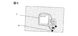
図5に示すように、検出回路9は、検出用小滴を互いに接続しているため、回路または1つの検出用小滴への如何なる攻撃によっても回路9が切断される。これにより、警報、たとえばチップ1の記憶装置に格納された秘密の破壊に使用可能なものが発生する。
検出回路9は、基板3の内層に埋め込まれているのが好ましく、この場合は、アクセス不可能と見なされる。そして、この回路は、導電性フィードスルー(図示せず)を介して基板3の表面まで「上に延び」ている。このように、1つの小滴によって2つのフィードスルーと小滴群とが接続されていることにより、検出回路は閉じた状態となる。機密領域への侵入の検出効果を十分に確保するため、小滴10および連結パッド6、ならびにそれぞれの相互接続配線は、製造コストへの要求を考慮して、可能な限りサイズを抑える必要があることは言うまでもない。
As shown in FIG. 5, since the
The
したがって、現在の回路形成技術で容易に実現可能な寸法は、小滴10については直径500μm前後、連結パッド6については200μm前後、検出回路9の相互接続配線については35μm前後である。また、小滴の堆積精度は25μm前後であり、小滴10と保護対象の最も近い連結パッド6との間の距離は50μm前後である。
なお、チップ1を基板3上に接着するのに使用する製品は一般に、注射器によって小滴状またはパターン状に基板表面に堆積される。このような製品としては、たとえば「ablestik ablebond (登録商標) epoxy 8290」という商標名で知られている導電性樹脂が挙げられる。小滴を堆積させるこの方法および工具は、導電性樹脂の小滴10を基板3上に堆積させる場合にも使用可能である。
Therefore, the dimensions that can be easily realized by the current circuit formation technology are about 500 μm in diameter for the
It should be noted that the product used to bond the
前述の通り、基板上に配置されたチップを有するコンポーネントの最機密領域は、脆弱要素、たとえば導電性材料の小滴10の形態で具現化されたものを近接させることによって保護される。以下では、特にコンポーネントへの機械的および/または化学的な攻撃に際して、所望の脆弱性を得るいくつかの方法を述べる。
この考え方では、チップまたはハウジングの基板上にある信号へのアクセスを試みる攻撃者が、まず第一に不活性層(通常は成形用樹脂)を化学的および/または機械的に除去する必要があるという保護原理が期待される。この不活性層を除去する動作によって、少なくとも1つの脆弱要素が破壊され、攻撃の検出動作が起動することになる。
As described above, the most sensitive area of a component having a chip disposed on a substrate is protected by bringing in close proximity a fragile element, such as that embodied in the form of a
This concept requires an attacker attempting to access signals on the chip or housing substrate to first remove the inert layer (usually the molding resin) chemically and / or mechanically. The protection principle is expected. By the operation of removing the inactive layer, at least one fragile element is destroyed, and an attack detection operation is started.
機械的脆弱性の導入に関しては、微細小滴10を堆積させる場合と同様に、微小サイズの脆弱領域を堆積させる場合に特有の方式である。これは、小滴のサイズを小さくすると、機密要素へアクセスするための如何なる機械加工アプローチ(たとえばフライス加工、ドリル加工等)に対しても感度が高くなるためであり、この機密要素への如何なる攻撃によっても、小滴の引裂が発生する可能性は極めて高くなる。
The introduction of mechanical weakness is a method peculiar to the case of depositing a micro-fragile region as in the case of depositing the
化学的脆弱性の導入に関しては、たとえば代表的には小滴10である脆弱要素の化学組成とハウジングの化学組成とが類似するものとすることが可能である。化学的攻撃はチップと基板とを内蔵および保護する、コンポーネントのハウジング(図示せず)を破壊することであるため、このような攻撃に対して敏感になることになる。
このように、ハウジングに対する化学的攻撃は、ハウジングの溶解と同時またはそれ以前に脆弱要素を破壊または劣化させることになる。この結果、検出回路が反応して攻撃が検出される。
With respect to the introduction of chemical vulnerability, the chemical composition of the brittle element, which is typically a
Thus, a chemical attack on the housing will destroy or degrade the fragile element at the same time or prior to the dissolution of the housing. As a result, the detection circuit reacts to detect an attack.
別の解決手段として、ハウジングの化学組成と脆弱要素の化学組成とが類似しない場合は、導電性の脆弱要素と絶縁性の脆弱要素とを混合する。この種の実施態様の一例としては、導電性エポキシ樹脂および絶縁性エポキシ樹脂を使用する。これにより、絶縁性エポキシ樹脂を除去しようとすると、導電性エポキシ樹脂も除去されることになる。樹脂を堆積させるための工具(ニードル)が集積回路の封入ラインで既存かつ利用可能であるため、エポキシ樹脂の使用は、非常に興味深い解決手段である。 As another solution, if the chemical composition of the housing and the chemical composition of the fragile element are not similar, the conductive fragile element and the insulating fragile element are mixed. As an example of this type of embodiment, a conductive epoxy resin and an insulating epoxy resin are used. Thus, when the insulating epoxy resin is removed, the conductive epoxy resin is also removed. The use of epoxy resin is a very interesting solution because the tool (needle) for depositing the resin is existing and available in the integrated circuit encapsulation line.
化学的攻撃を困難にする最後の手段としては、攻撃者が脆弱要素および/またはハウジングを攻撃する際の製品の選択肢を狭めることが挙げられる。これは、ハウジングの化学組成として多量のシリカを含む場合、有機溶媒の効果がなくなるためである。したがって、これらの条件下では、樹脂を破壊して集積回路を攻撃するのに通常使用される発煙硝酸等の製品のみが使用可能である。硝酸、導電性を確保するのに十分な濃度を有するその他任意の酸、または任意の導電性溶液を考慮して、閉じていない状態の回路を用いた検出機構をハウジング内に設ければ十分である。これにより、攻撃用溶液の流動性および導電性のため、この導電性溶液が拡散すると、検出回路が閉じた状態となって攻撃が報知されるという効果を奏することになる。 A last resort to make chemical attacks difficult is to narrow product options when attackers attack fragile elements and / or housings. This is because when the housing contains a large amount of silica as the chemical composition, the effect of the organic solvent is lost. Therefore, under these conditions, only products such as fuming nitric acid that are normally used to destroy the resin and attack the integrated circuit can be used. Considering nitric acid, any other acid with sufficient concentration to ensure conductivity, or any conductive solution, it is sufficient to provide a detection mechanism in the housing that uses an unclosed circuit. is there. As a result, due to the fluidity and conductivity of the attack solution, when this conductive solution diffuses, the detection circuit is closed and an attack is notified.
脆弱要素は、当該要素のために確保された接続点の位置を除いて、電気的に絶縁された表面上に堆積される。
また、脆弱要素の位置および/または散在は、個別に規定されるべきセキュリティの水準および最適な技術的選択に応じて、大きく異なっていてもよい。
たとえば、各脆弱要素10は、近接して機密領域を保護するため、当該領域の近くに配置されていてもよい。ワイヤ相互接続を利用する場合は、チップに接続するワイヤの基板への連結点である連結パッドを保護する必要がある。したがって、脆弱要素は、これら連結パッドに可能な限り近づけて堆積される。脆弱要素は、連結パッドに接触させるのが理想的である。こうすれば、攻撃を試みる者は、検出されることなく連結パッドにアクセスして攻撃を仕掛けることが非常に難しくなる。
The fragile element is deposited on an electrically isolated surface except for the location of the connection point reserved for the element.
Also, the location and / or distribution of fragile elements may vary greatly depending on the level of security to be individually defined and the optimal technical choice.
For example, each
以上のことから、脆弱要素の散在は、通常「メッシュ」と呼ばれるパターン状であってもよい。これは、程度の差はあるものの、綿密に編み込んだネットワークの一種であって、基板の全体または一部にわたって散在している。これにより、基板中を伝達する信号の保護が可能となる。また、回路がこのように形成されることにより、回路中を伝わる信号の変形により、如何なる侵入も検出可能となる。 From the above, the scattered fragile elements may be in a pattern shape generally called “mesh”. This is a type of network that is closely woven, to varying degrees, and is scattered over the whole or part of the substrate. Thereby, the signal transmitted through the substrate can be protected. Further, since the circuit is formed in this way, any intrusion can be detected by deformation of a signal transmitted through the circuit.
脆弱要素の別の散在パターンとしては、基板上に脆弱要素の微小ドットを散在させたパターンが挙げられる。たとえば、脆弱要素は、基板全体に不規則に分布させてもよいし、または、特に機密性が高く保護すべき部分のみに分布させてもよい。このパターンの場合、検出回路の大部分は基板中に埋め込まれ、わずかな点のみが外部に現れることになる。そして、これらの点には、導電性小滴等の脆弱要素が堆積される。検出回路がこのように形成されることにより、当該回路中を伝わる信号の変形により、如何なる侵入も検出可能となる。 Another scattered pattern of fragile elements includes a pattern in which minute dots of fragile elements are scattered on a substrate. For example, the fragile elements may be distributed randomly throughout the substrate, or may be distributed only in areas that are particularly sensitive and should be protected. In the case of this pattern, most of the detection circuit is embedded in the substrate, and only a few points appear outside. At these points, fragile elements such as conductive droplets are deposited. By forming the detection circuit in this way, any intrusion can be detected by the deformation of the signal transmitted through the circuit.
第3の実施例としては、基板ではなくチップを直接保護する形態が挙げられる。チップは通常、絶縁性のパッシベーション層で覆われている。これにより、導電性の脆弱要素をチップ表面上に堆積させることができる。そして、検出回路との接続は、チップのスタッド2で行う。非常に簡単な実施態様としては、連続する2つのスタッド間の接続がある。このような検出回路であれば、これら2つのスタッドの近傍に配置された第3の機密スタッドを保護することができる。この種の製品の利点は、脆弱要素を堆積させることによる2つのスタッドの接続が、容易に実現可能であることである。また、チップ表面上の任意の位置にパッシベーション開口を形成し、小滴を堆積させることも可能である。
As a third embodiment, there is a form in which a chip, not a substrate, is directly protected. The chip is usually covered with an insulating passivation layer. Thereby, a conductive weak element can be deposited on the chip surface. The detection circuit is connected to the
検出回路の第4の実施例としては、初期的には開放状態にあるが攻撃液体(たとえば発煙硝酸等)の流動性および導電性によって閉じられる回路を用いて、上述の溶液と同様に、攻撃液体の導電性を利用してチップを直接保護する形態が挙げられる。これは、チップ表面上に分散して1または複数の開回路を構成するスタッドの形態で実現可能である。これらの開回路は、攻撃液体が拡がると、その流動性および導電性によって閉じた状態となる。表面上のスタッドの密度は可変であり、高密度とすることで液体による化学的攻撃を完全に防止するようにしてもよい。 As a fourth embodiment of the detection circuit, using a circuit that is initially open but is closed by the fluidity and conductivity of the attack liquid (eg fuming nitric acid), The form which protects a chip | tip directly using the electroconductivity of a liquid is mentioned. This can be realized in the form of studs that are distributed on the chip surface to form one or more open circuits. These open circuits are closed due to their fluidity and conductivity when the attack liquid spreads. The density of studs on the surface is variable, and chemical attack by liquid may be completely prevented by increasing the density.
この最後の解決手段には、2つの効果がある。第1の効果として、ハウジング内ではチップが基板よりも高いため、ハウジングへの攻撃は、チップ表面上に配置されたセンサーによって早く検出される。第2の効果として、この機構は、チップへの物理的な侵入に対する保護も可能とする。また、理想的には、現在一般的なラティス等の機構と併せて使用してもよい。
発明の効果:
本発明により得られた集積回路の保護方法および集積回路は、設定した目的を満足する。提案した解決手段では、機密領域の近傍に脆弱要素を使用しているため、集積回路で利用している技術に関わらず、集積回路に対する実質的にすべての侵入攻撃に対抗可能である。
This last solution has two effects. As a first effect, since the chip is higher than the substrate in the housing, the attack on the housing is quickly detected by a sensor disposed on the chip surface. As a second effect, this mechanism also allows protection against physical intrusion into the chip. Also, ideally, it may be used in combination with a mechanism such as a currently common lattice.
The invention's effect:
The integrated circuit protection method and integrated circuit obtained by the present invention satisfy the set purpose. Since the proposed solution uses a vulnerable element in the vicinity of the confidential area, it can counter virtually all intrusion attacks on the integrated circuit, regardless of the technology used in the integrated circuit.
また、この解決手段により、集積回路のハウジング領域の保護を補強できるため、セキュリティを容易に利用かつ保証可能である。
さらに、たとえば脆弱要素がエポキシ樹脂製である場合等は、樹脂堆積用の工具が既存であり十分使いこなすことができるため、別の機能に使用する場合、すなわち検出回路を形成し、侵入に対して閉じた状態となるように導電性小滴を堆積させる場合であっても、ほとんどコストが掛からずに高い生産収率が得られるものと考えられる。
発明の用途:
本発明の複数の利点を考慮すると、上述の解決手段は、たとえばボイスオーバーIP電話、ネットワーク上での機密データの送信(認証、VPN技術)、安全な認証トークン(「セキュアUSBキー」)、セキュリティ専用コンポーネント、暗号演算用コンポーネント等の応用向け機密コンポーネント等、広範な用途を対象とした集積回路に適用可能である。
Further, this solution can reinforce the protection of the housing area of the integrated circuit, so that security can be easily used and guaranteed.
Furthermore, for example, when the fragile element is made of an epoxy resin, a resin deposition tool is already available and can be fully used, so when used for another function, that is, a detection circuit is formed, Even when conductive droplets are deposited so as to be in a closed state, it is considered that a high production yield can be obtained with little cost.
Use of invention:
In view of the advantages of the present invention, the above solutions include, for example, voice over IP phones, transmission of sensitive data over the network (authentication, VPN technology), secure authentication token (“secure USB key”), security The present invention can be applied to integrated circuits for a wide range of applications such as dedicated components and confidential components for applications such as cryptographic operation components.
Claims (9)
前記ハウジングの内部への機械的および/もしくは化学的侵入ならびに/または集積回路の機密領域へアクセスしようとする試みを検出可能な少なくとも1つの侵入検出手段(9、10)と、を備えた電子集積回路であって、
前記侵入検出手段(9、10)が、検出回路(9)を備えており、この検出回路(9)は、当該集積回路の複数の前記機密領域のうちの1つの領域へアクセスしようとする如何なる試みによっても当該検出回路(9)の電気的閉/開状態が変化するように、前記基板(3)に内蔵および/または載置されるとともに、当該集積回路の前記機密領域のごく近傍を通過するように配置されていることを特徴とする電子集積回路。 An electronic chip (1) comprising an input / output stud (2) connected to a connecting pad (6) disposed on a substrate (3), and attached to the substrate in a state protected by a housing;
Electronic integration with at least one intrusion detection means (9, 10) capable of detecting mechanical and / or chemical intrusion into the interior of the housing and / or attempts to access a sensitive area of the integrated circuit A circuit,
The intrusion detection means (9, 10) is provided with a detection circuit (9), and this detection circuit (9) is capable of any one trying to access one of the plurality of confidential areas of the integrated circuit. It is built in and / or mounted on the substrate (3) so that the electrical closed / open state of the detection circuit (9) changes even if it is attempted, and passes through the vicinity of the confidential area of the integrated circuit. An electronic integrated circuit, wherein the electronic integrated circuit is arranged as described above.
Applications Claiming Priority (3)
| Application Number | Priority Date | Filing Date | Title |
|---|---|---|---|
| FR0806563A FR2938953B1 (en) | 2008-11-21 | 2008-11-21 | DEVICE FOR PROTECTING AN ELECTRONIC INTEGRATED CIRCUIT BOX FROM PHYSICAL OR CHEMICAL INTRUSIONS. |
| FR0806563 | 2008-11-21 | ||
| PCT/FR2009/001307 WO2010058094A1 (en) | 2008-11-21 | 2009-11-14 | Device for protecting an electronic integrated circuit housing against physical or chemical ingression |
Publications (2)
| Publication Number | Publication Date |
|---|---|
| JP2012509585A true JP2012509585A (en) | 2012-04-19 |
| JP5933266B2 JP5933266B2 (en) | 2016-06-08 |
Family
ID=40752530
Family Applications (1)
| Application Number | Title | Priority Date | Filing Date |
|---|---|---|---|
| JP2011536917A Expired - Fee Related JP5933266B2 (en) | 2008-11-21 | 2009-11-14 | Device for protecting an electronic integrated circuit housing against physical or chemical intrusion |
Country Status (5)
| Country | Link |
|---|---|
| US (1) | US8581251B2 (en) |
| JP (1) | JP5933266B2 (en) |
| CN (1) | CN102257516B (en) |
| FR (1) | FR2938953B1 (en) |
| WO (1) | WO2010058094A1 (en) |
Cited By (1)
| Publication number | Priority date | Publication date | Assignee | Title |
|---|---|---|---|---|
| JP2015501460A (en) * | 2012-08-31 | 2015-01-15 | ブルーバード インコーポレイテッド | Mobile terminal |
Families Citing this family (11)
| Publication number | Priority date | Publication date | Assignee | Title |
|---|---|---|---|---|
| CN102858082B (en) * | 2012-09-26 | 2015-06-10 | 深圳市九思泰达技术有限公司 | Protective structure for safe area of core module |
| US10651135B2 (en) * | 2016-06-28 | 2020-05-12 | Marvell Asia Pte, Ltd. | Tamper detection for a chip package |
| EP3340114B1 (en) * | 2016-12-22 | 2020-09-30 | EM Microelectronic-Marin SA | Rfid circuit with two communication frequencies provided with a tamper-proof loop |
| US11454010B2 (en) | 2017-03-09 | 2022-09-27 | Charles James SPOFFORD | Appliance with shim compatible geometry |
| CN107133535A (en) * | 2017-04-13 | 2017-09-05 | 上海汇尔通信息技术有限公司 | data protection structure and mobile terminal device |
| US11289443B2 (en) * | 2017-04-20 | 2022-03-29 | Palo Alto Research Center Incorporated | Microspring structure for hardware trusted platform module |
| FR3084521B1 (en) | 2018-07-25 | 2020-08-14 | Stmicroelectronics Rousset | PROTECTION PROCESS OF AN INTEGRATED CIRCUIT MODULE AND CORRESPONDING DEVICE |
| FR3084520B1 (en) | 2018-07-25 | 2020-08-14 | Stmicroelectronics Rousset | PROTECTION METHOD FOR AN INTEGRATED CIRCUIT, AND CORRESPONDING DEVICE |
| FR3084492A1 (en) | 2018-07-30 | 2020-01-31 | Stmicroelectronics (Rousset) Sas | METHOD FOR DETECTING AN ATTACK BY A BEAM OF ELECTRICALLY CHARGED PARTICLES ON AN INTEGRATED CIRCUIT, AND CORRESPONDING INTEGRATED CIRCUIT |
| FR3099259B1 (en) * | 2019-07-24 | 2021-08-13 | St Microelectronics Rousset | Method for protecting data stored in a memory, and corresponding integrated circuit |
| WO2022027535A1 (en) * | 2020-08-07 | 2022-02-10 | 深圳市汇顶科技股份有限公司 | Security chip and electronic device |
Citations (5)
| Publication number | Priority date | Publication date | Assignee | Title |
|---|---|---|---|---|
| JPS62501242A (en) * | 1984-12-21 | 1987-05-14 | エヌ・シ−・ア−ル・コ−ポレ−シヨン | Safeguards for storing sensitive data |
| JPH10294325A (en) * | 1997-02-24 | 1998-11-04 | General Instr Corp | Tampering preventive bonding wire for integrated circuit use |
| WO2007003228A1 (en) * | 2005-06-30 | 2007-01-11 | Siemens Aktiengesellschaft | Hardware protection system for sensitive electronic-data modules protecting against external manipulations |
| US20070018334A1 (en) * | 2005-07-21 | 2007-01-25 | Alain Peytavy | Security method for data protection |
| JP2007533129A (en) * | 2004-04-08 | 2007-11-15 | ダブリュ.エル.ゴア アンド アソシエーツ(ユーケー)リミティド | Tamper-open reaction covering |
Family Cites Families (14)
| Publication number | Priority date | Publication date | Assignee | Title |
|---|---|---|---|---|
| US5027397A (en) * | 1989-09-12 | 1991-06-25 | International Business Machines Corporation | Data protection by detection of intrusion into electronic assemblies |
| US6708274B2 (en) | 1998-04-30 | 2004-03-16 | Intel Corporation | Cryptographically protected paging subsystem |
| FR2801999A1 (en) * | 1999-12-01 | 2001-06-08 | Gemplus Card Int | Smart card with integrated circuit chips includes additional conductive mesh providing protection against fraudulent access to chips |
| GB2363233B (en) * | 2000-05-11 | 2004-03-31 | Ibm | Tamper resistant card enclosure with improved intrusion detection circuit |
| DE10044837C1 (en) * | 2000-09-11 | 2001-09-13 | Infineon Technologies Ag | Tampering detection circuit for IC has detection circuit coupled to signal line and at least one line pair extending between separate circuit blocks of IC |
| US7490250B2 (en) * | 2001-10-26 | 2009-02-10 | Lenovo (Singapore) Pte Ltd. | Method and system for detecting a tamper event in a trusted computing environment |
| US7266842B2 (en) | 2002-04-18 | 2007-09-04 | International Business Machines Corporation | Control function implementing selective transparent data authentication within an integrated system |
| FR2864667B1 (en) * | 2003-12-29 | 2006-02-24 | Commissariat Energie Atomique | PROTECTING AN INTEGRATED CIRCUIT CHIP CONTAINING CONFIDENTIAL DATA |
| FR2872610B1 (en) * | 2004-07-02 | 2007-06-08 | Commissariat Energie Atomique | DEVICE FOR SECURING COMPONENTS |
| US7979721B2 (en) * | 2004-11-15 | 2011-07-12 | Microsoft Corporation | Enhanced packaging for PC security |
| DE102005042790B4 (en) * | 2005-09-08 | 2010-11-18 | Infineon Technologies Ag | Integrated circuit arrangement and method for operating such |
| US8522051B2 (en) * | 2007-05-07 | 2013-08-27 | Infineon Technologies Ag | Protection for circuit boards |
| EP2026470A1 (en) | 2007-08-17 | 2009-02-18 | Panasonic Corporation | Running cyclic redundancy check over coding segments |
| JP5041980B2 (en) * | 2007-11-16 | 2012-10-03 | ルネサスエレクトロニクス株式会社 | Data processing circuit and communication portable terminal device |
-
2008
- 2008-11-21 FR FR0806563A patent/FR2938953B1/en active Active
-
2009
- 2009-11-14 US US13/130,534 patent/US8581251B2/en active Active
- 2009-11-14 CN CN200980146866.0A patent/CN102257516B/en active Active
- 2009-11-14 JP JP2011536917A patent/JP5933266B2/en not_active Expired - Fee Related
- 2009-11-14 WO PCT/FR2009/001307 patent/WO2010058094A1/en active Application Filing
Patent Citations (5)
| Publication number | Priority date | Publication date | Assignee | Title |
|---|---|---|---|---|
| JPS62501242A (en) * | 1984-12-21 | 1987-05-14 | エヌ・シ−・ア−ル・コ−ポレ−シヨン | Safeguards for storing sensitive data |
| JPH10294325A (en) * | 1997-02-24 | 1998-11-04 | General Instr Corp | Tampering preventive bonding wire for integrated circuit use |
| JP2007533129A (en) * | 2004-04-08 | 2007-11-15 | ダブリュ.エル.ゴア アンド アソシエーツ(ユーケー)リミティド | Tamper-open reaction covering |
| WO2007003228A1 (en) * | 2005-06-30 | 2007-01-11 | Siemens Aktiengesellschaft | Hardware protection system for sensitive electronic-data modules protecting against external manipulations |
| US20070018334A1 (en) * | 2005-07-21 | 2007-01-25 | Alain Peytavy | Security method for data protection |
Cited By (1)
| Publication number | Priority date | Publication date | Assignee | Title |
|---|---|---|---|---|
| JP2015501460A (en) * | 2012-08-31 | 2015-01-15 | ブルーバード インコーポレイテッド | Mobile terminal |
Also Published As
| Publication number | Publication date |
|---|---|
| FR2938953B1 (en) | 2011-03-11 |
| JP5933266B2 (en) | 2016-06-08 |
| WO2010058094A1 (en) | 2010-05-27 |
| US8581251B2 (en) | 2013-11-12 |
| CN102257516B (en) | 2015-10-07 |
| US20110260162A1 (en) | 2011-10-27 |
| CN102257516A (en) | 2011-11-23 |
| FR2938953A1 (en) | 2010-05-28 |
Similar Documents
| Publication | Publication Date | Title |
|---|---|---|
| JP5933266B2 (en) | Device for protecting an electronic integrated circuit housing against physical or chemical intrusion | |
| JP5647681B2 (en) | Multi-layer secure structure | |
| US7054162B2 (en) | Security module system, apparatus and process | |
| TW202312358A (en) | Protective semiconductor elements for bonded structures | |
| US5880523A (en) | Anti-tamper integrated circuit | |
| US5406630A (en) | Tamperproof arrangement for an integrated circuit device | |
| WO2020210703A1 (en) | Protective elements for bonded structures | |
| JPH10294325A (en) | Tampering preventive bonding wire for integrated circuit use | |
| US7812428B2 (en) | Secure connector grid array package | |
| US20090040735A1 (en) | Tamper Respondent System | |
| US10181430B2 (en) | Tamper resistant electronic hardware assembly with a non-functional die used as a protective layer | |
| US7633149B2 (en) | Integrated circuit arrangement | |
| JPH11504164A (en) | Chip cover | |
| US11894315B2 (en) | Electronic system in package comprising protected side faces | |
| JP4836995B2 (en) | Integrated circuit module | |
| US20230222251A1 (en) | Integrated circuit device with protection against malicious attacks | |
| JP4181068B2 (en) | Integrated circuit module | |
| US7436072B2 (en) | Protected chip stack | |
| MXPA98001451A (en) | Circuit integrated to proof of violation |
Legal Events
| Date | Code | Title | Description |
|---|---|---|---|
| RD04 | Notification of resignation of power of attorney |
Free format text: JAPANESE INTERMEDIATE CODE: A7424 Effective date: 20120629 |
|
| A621 | Written request for application examination |
Free format text: JAPANESE INTERMEDIATE CODE: A621 Effective date: 20121018 |
|
| A977 | Report on retrieval |
Free format text: JAPANESE INTERMEDIATE CODE: A971007 Effective date: 20130808 |
|
| A131 | Notification of reasons for refusal |
Free format text: JAPANESE INTERMEDIATE CODE: A131 Effective date: 20131128 |
|
| A521 | Request for written amendment filed |
Free format text: JAPANESE INTERMEDIATE CODE: A523 Effective date: 20140227 |
|
| A02 | Decision of refusal |
Free format text: JAPANESE INTERMEDIATE CODE: A02 Effective date: 20140911 |
|
| A521 | Request for written amendment filed |
Free format text: JAPANESE INTERMEDIATE CODE: A523 Effective date: 20150113 |
|
| A521 | Request for written amendment filed |
Free format text: JAPANESE INTERMEDIATE CODE: A821 Effective date: 20150114 |
|
| A911 | Transfer to examiner for re-examination before appeal (zenchi) |
Free format text: JAPANESE INTERMEDIATE CODE: A911 Effective date: 20150205 |
|
| A912 | Re-examination (zenchi) completed and case transferred to appeal board |
Free format text: JAPANESE INTERMEDIATE CODE: A912 Effective date: 20150410 |
|
| A521 | Request for written amendment filed |
Free format text: JAPANESE INTERMEDIATE CODE: A523 Effective date: 20160222 |
|
| A61 | First payment of annual fees (during grant procedure) |
Free format text: JAPANESE INTERMEDIATE CODE: A61 Effective date: 20160502 |
|
| R150 | Certificate of patent or registration of utility model |
Ref document number: 5933266 Country of ref document: JP Free format text: JAPANESE INTERMEDIATE CODE: R150 |
|
| R250 | Receipt of annual fees |
Free format text: JAPANESE INTERMEDIATE CODE: R250 |
|
| R250 | Receipt of annual fees |
Free format text: JAPANESE INTERMEDIATE CODE: R250 |
|
| R250 | Receipt of annual fees |
Free format text: JAPANESE INTERMEDIATE CODE: R250 |
|
| LAPS | Cancellation because of no payment of annual fees |