JP2012509201A - Method for forming micro surface structure, method for manufacturing micro electro mechanical member, micro surface structure, and micro electro mechanical member having the structure - Google Patents
Method for forming micro surface structure, method for manufacturing micro electro mechanical member, micro surface structure, and micro electro mechanical member having the structure Download PDFInfo
- Publication number
- JP2012509201A JP2012509201A JP2011543766A JP2011543766A JP2012509201A JP 2012509201 A JP2012509201 A JP 2012509201A JP 2011543766 A JP2011543766 A JP 2011543766A JP 2011543766 A JP2011543766 A JP 2011543766A JP 2012509201 A JP2012509201 A JP 2012509201A
- Authority
- JP
- Japan
- Prior art keywords
- substrate
- functional material
- micro
- getter
- ridge
- Prior art date
- Legal status (The legal status is an assumption and is not a legal conclusion. Google has not performed a legal analysis and makes no representation as to the accuracy of the status listed.)
- Granted
Links
- 238000000034 method Methods 0.000 title claims abstract description 56
- 238000004519 manufacturing process Methods 0.000 title claims abstract description 14
- 239000000463 material Substances 0.000 claims abstract description 139
- 239000000758 substrate Substances 0.000 claims abstract description 112
- 239000010410 layer Substances 0.000 claims description 67
- 238000007373 indentation Methods 0.000 claims description 38
- 239000007787 solid Substances 0.000 claims description 29
- 230000003287 optical effect Effects 0.000 claims description 11
- 238000005530 etching Methods 0.000 claims description 9
- PCHJSUWPFVWCPO-UHFFFAOYSA-N gold Chemical compound [Au] PCHJSUWPFVWCPO-UHFFFAOYSA-N 0.000 claims description 8
- 229910052737 gold Inorganic materials 0.000 claims description 8
- 239000010931 gold Substances 0.000 claims description 8
- 230000006911 nucleation Effects 0.000 claims description 8
- 238000010899 nucleation Methods 0.000 claims description 8
- 239000011248 coating agent Substances 0.000 claims description 7
- 239000011247 coating layer Substances 0.000 claims description 7
- 238000000576 coating method Methods 0.000 claims description 7
- 239000002966 varnish Substances 0.000 claims description 7
- 239000006117 anti-reflective coating Substances 0.000 claims description 6
- 238000001465 metallisation Methods 0.000 claims description 6
- 230000008569 process Effects 0.000 claims description 6
- 238000007740 vapor deposition Methods 0.000 claims description 6
- 239000000126 substance Substances 0.000 claims description 5
- 229910004298 SiO 2 Inorganic materials 0.000 claims description 3
- 230000003667 anti-reflective effect Effects 0.000 claims description 3
- 239000003989 dielectric material Substances 0.000 claims description 3
- 229910018072 Al 2 O 3 Inorganic materials 0.000 claims description 2
- 239000011159 matrix material Substances 0.000 claims description 2
- 229910017083 AlN Inorganic materials 0.000 claims 1
- 229910004541 SiN Inorganic materials 0.000 claims 1
- 238000005516 engineering process Methods 0.000 abstract description 7
- 238000010276 construction Methods 0.000 abstract description 2
- 238000005304 joining Methods 0.000 abstract description 2
- 239000007789 gas Substances 0.000 description 29
- 229910052751 metal Inorganic materials 0.000 description 17
- 239000002184 metal Substances 0.000 description 17
- 229910052719 titanium Inorganic materials 0.000 description 13
- RTAQQCXQSZGOHL-UHFFFAOYSA-N Titanium Chemical compound [Ti] RTAQQCXQSZGOHL-UHFFFAOYSA-N 0.000 description 12
- 238000007789 sealing Methods 0.000 description 12
- 239000010936 titanium Substances 0.000 description 12
- BASFCYQUMIYNBI-UHFFFAOYSA-N platinum Chemical compound [Pt] BASFCYQUMIYNBI-UHFFFAOYSA-N 0.000 description 10
- 239000000956 alloy Substances 0.000 description 7
- 229910045601 alloy Inorganic materials 0.000 description 7
- PXHVJJICTQNCMI-UHFFFAOYSA-N Nickel Chemical compound [Ni] PXHVJJICTQNCMI-UHFFFAOYSA-N 0.000 description 6
- 125000004429 atom Chemical group 0.000 description 6
- 238000006243 chemical reaction Methods 0.000 description 6
- 238000001312 dry etching Methods 0.000 description 6
- 238000000926 separation method Methods 0.000 description 6
- 239000010409 thin film Substances 0.000 description 6
- 150000002739 metals Chemical class 0.000 description 5
- 229910052697 platinum Inorganic materials 0.000 description 5
- 238000004544 sputter deposition Methods 0.000 description 5
- XKRFYHLGVUSROY-UHFFFAOYSA-N Argon Chemical compound [Ar] XKRFYHLGVUSROY-UHFFFAOYSA-N 0.000 description 4
- IJGRMHOSHXDMSA-UHFFFAOYSA-N Atomic nitrogen Chemical compound N#N IJGRMHOSHXDMSA-UHFFFAOYSA-N 0.000 description 4
- 239000004020 conductor Substances 0.000 description 4
- 230000000694 effects Effects 0.000 description 4
- 238000001704 evaporation Methods 0.000 description 4
- 239000008204 material by function Substances 0.000 description 4
- 229910052756 noble gas Inorganic materials 0.000 description 4
- 239000002245 particle Substances 0.000 description 4
- 238000001994 activation Methods 0.000 description 3
- 230000015572 biosynthetic process Effects 0.000 description 3
- 229910021418 black silicon Inorganic materials 0.000 description 3
- 238000000151 deposition Methods 0.000 description 3
- 239000010408 film Substances 0.000 description 3
- 238000001459 lithography Methods 0.000 description 3
- 238000005259 measurement Methods 0.000 description 3
- 229910052759 nickel Inorganic materials 0.000 description 3
- 150000004767 nitrides Chemical class 0.000 description 3
- 238000007747 plating Methods 0.000 description 3
- XLYOFNOQVPJJNP-UHFFFAOYSA-N water Chemical compound O XLYOFNOQVPJJNP-UHFFFAOYSA-N 0.000 description 3
- 230000004913 activation Effects 0.000 description 2
- 238000013459 approach Methods 0.000 description 2
- 229910052786 argon Inorganic materials 0.000 description 2
- QVGXLLKOCUKJST-UHFFFAOYSA-N atomic oxygen Chemical compound [O] QVGXLLKOCUKJST-UHFFFAOYSA-N 0.000 description 2
- 230000008901 benefit Effects 0.000 description 2
- 230000008859 change Effects 0.000 description 2
- 238000005229 chemical vapour deposition Methods 0.000 description 2
- 230000008021 deposition Effects 0.000 description 2
- 238000001514 detection method Methods 0.000 description 2
- 230000005496 eutectics Effects 0.000 description 2
- 230000008020 evaporation Effects 0.000 description 2
- 125000000524 functional group Chemical group 0.000 description 2
- 239000001257 hydrogen Substances 0.000 description 2
- 229910052739 hydrogen Inorganic materials 0.000 description 2
- 230000003993 interaction Effects 0.000 description 2
- 230000007774 longterm Effects 0.000 description 2
- VNWKTOKETHGBQD-UHFFFAOYSA-N methane Chemical compound C VNWKTOKETHGBQD-UHFFFAOYSA-N 0.000 description 2
- 229910052757 nitrogen Inorganic materials 0.000 description 2
- 238000010943 off-gassing Methods 0.000 description 2
- 239000001301 oxygen Substances 0.000 description 2
- 229910052760 oxygen Inorganic materials 0.000 description 2
- 238000012876 topography Methods 0.000 description 2
- UFHFLCQGNIYNRP-UHFFFAOYSA-N Hydrogen Chemical compound [H][H] UFHFLCQGNIYNRP-UHFFFAOYSA-N 0.000 description 1
- 229910000577 Silicon-germanium Inorganic materials 0.000 description 1
- 229910010038 TiAl Inorganic materials 0.000 description 1
- 229910010165 TiCu Inorganic materials 0.000 description 1
- 229910008484 TiSi Inorganic materials 0.000 description 1
- -1 TiTiNAu Inorganic materials 0.000 description 1
- 229910008651 TiZr Inorganic materials 0.000 description 1
- ATJFFYVFTNAWJD-UHFFFAOYSA-N Tin Chemical compound [Sn] ATJFFYVFTNAWJD-UHFFFAOYSA-N 0.000 description 1
- 229910007880 ZrAl Inorganic materials 0.000 description 1
- 229910008008 ZrCo Inorganic materials 0.000 description 1
- LEVVHYCKPQWKOP-UHFFFAOYSA-N [Si].[Ge] Chemical compound [Si].[Ge] LEVVHYCKPQWKOP-UHFFFAOYSA-N 0.000 description 1
- 238000010521 absorption reaction Methods 0.000 description 1
- 239000002313 adhesive film Substances 0.000 description 1
- 229910052782 aluminium Inorganic materials 0.000 description 1
- 229910021417 amorphous silicon Inorganic materials 0.000 description 1
- 229910052788 barium Inorganic materials 0.000 description 1
- 230000015556 catabolic process Effects 0.000 description 1
- 239000003054 catalyst Substances 0.000 description 1
- 229910052804 chromium Inorganic materials 0.000 description 1
- 238000004140 cleaning Methods 0.000 description 1
- 238000011109 contamination Methods 0.000 description 1
- 238000004320 controlled atmosphere Methods 0.000 description 1
- 230000008878 coupling Effects 0.000 description 1
- 238000010168 coupling process Methods 0.000 description 1
- 238000005859 coupling reaction Methods 0.000 description 1
- 238000000354 decomposition reaction Methods 0.000 description 1
- 230000007547 defect Effects 0.000 description 1
- 238000006731 degradation reaction Methods 0.000 description 1
- 230000032798 delamination Effects 0.000 description 1
- 230000003111 delayed effect Effects 0.000 description 1
- 230000001419 dependent effect Effects 0.000 description 1
- 230000001627 detrimental effect Effects 0.000 description 1
- 238000011161 development Methods 0.000 description 1
- 238000010586 diagram Methods 0.000 description 1
- 238000005566 electron beam evaporation Methods 0.000 description 1
- 238000011156 evaluation Methods 0.000 description 1
- 238000004299 exfoliation Methods 0.000 description 1
- 238000009501 film coating Methods 0.000 description 1
- JVPLOXQKFGYFMN-UHFFFAOYSA-N gold tin Chemical compound [Sn].[Au] JVPLOXQKFGYFMN-UHFFFAOYSA-N 0.000 description 1
- 229910052735 hafnium Inorganic materials 0.000 description 1
- 150000002431 hydrogen Chemical class 0.000 description 1
- 230000001771 impaired effect Effects 0.000 description 1
- 238000010849 ion bombardment Methods 0.000 description 1
- 229910052742 iron Inorganic materials 0.000 description 1
- 229910052743 krypton Inorganic materials 0.000 description 1
- DNNSSWSSYDEUBZ-UHFFFAOYSA-N krypton atom Chemical compound [Kr] DNNSSWSSYDEUBZ-UHFFFAOYSA-N 0.000 description 1
- 229910052746 lanthanum Inorganic materials 0.000 description 1
- 150000002605 large molecules Chemical class 0.000 description 1
- 238000010147 laser engraving Methods 0.000 description 1
- 229920002521 macromolecule Polymers 0.000 description 1
- 238000012423 maintenance Methods 0.000 description 1
- 230000007246 mechanism Effects 0.000 description 1
- 238000004377 microelectronic Methods 0.000 description 1
- 239000000203 mixture Substances 0.000 description 1
- 150000002835 noble gases Chemical class 0.000 description 1
- 238000004806 packaging method and process Methods 0.000 description 1
- 229920002120 photoresistant polymer Polymers 0.000 description 1
- 229910021420 polycrystalline silicon Inorganic materials 0.000 description 1
- 239000012495 reaction gas Substances 0.000 description 1
- 230000009257 reactivity Effects 0.000 description 1
- 229920006395 saturated elastomer Polymers 0.000 description 1
- 230000009291 secondary effect Effects 0.000 description 1
- 238000001179 sorption measurement Methods 0.000 description 1
- 238000003860 storage Methods 0.000 description 1
- 238000005496 tempering Methods 0.000 description 1
- 238000002207 thermal evaporation Methods 0.000 description 1
- 229910001258 titanium gold Inorganic materials 0.000 description 1
- 229910052720 vanadium Inorganic materials 0.000 description 1
- 238000003631 wet chemical etching Methods 0.000 description 1
- 229910052724 xenon Inorganic materials 0.000 description 1
- FHNFHKCVQCLJFQ-UHFFFAOYSA-N xenon atom Chemical compound [Xe] FHNFHKCVQCLJFQ-UHFFFAOYSA-N 0.000 description 1
- 229910052845 zircon Inorganic materials 0.000 description 1
- 229910052726 zirconium Inorganic materials 0.000 description 1
- GFQYVLUOOAAOGM-UHFFFAOYSA-N zirconium(iv) silicate Chemical compound [Zr+4].[O-][Si]([O-])([O-])[O-] GFQYVLUOOAAOGM-UHFFFAOYSA-N 0.000 description 1
Images


Classifications
-
- B—PERFORMING OPERATIONS; TRANSPORTING
- B81—MICROSTRUCTURAL TECHNOLOGY
- B81C—PROCESSES OR APPARATUS SPECIALLY ADAPTED FOR THE MANUFACTURE OR TREATMENT OF MICROSTRUCTURAL DEVICES OR SYSTEMS
- B81C1/00—Manufacture or treatment of devices or systems in or on a substrate
- B81C1/00015—Manufacture or treatment of devices or systems in or on a substrate for manufacturing microsystems
- B81C1/00206—Processes for functionalising a surface, e.g. provide the surface with specific mechanical, chemical or biological properties
-
- B—PERFORMING OPERATIONS; TRANSPORTING
- B81—MICROSTRUCTURAL TECHNOLOGY
- B81B—MICROSTRUCTURAL DEVICES OR SYSTEMS, e.g. MICROMECHANICAL DEVICES
- B81B7/00—Microstructural systems; Auxiliary parts of microstructural devices or systems
- B81B7/0032—Packages or encapsulation
- B81B7/0035—Packages or encapsulation for maintaining a controlled atmosphere inside of the chamber containing the MEMS
- B81B7/0038—Packages or encapsulation for maintaining a controlled atmosphere inside of the chamber containing the MEMS using materials for controlling the level of pressure, contaminants or moisture inside of the package, e.g. getters
-
- G—PHYSICS
- G01—MEASURING; TESTING
- G01J—MEASUREMENT OF INTENSITY, VELOCITY, SPECTRAL CONTENT, POLARISATION, PHASE OR PULSE CHARACTERISTICS OF INFRARED, VISIBLE OR ULTRAVIOLET LIGHT; COLORIMETRY; RADIATION PYROMETRY
- G01J5/00—Radiation pyrometry, e.g. infrared or optical thermometry
- G01J5/02—Constructional details
- G01J5/04—Casings
- G01J5/041—Mountings in enclosures or in a particular environment
- G01J5/045—Sealings; Vacuum enclosures; Encapsulated packages; Wafer bonding structures; Getter arrangements
-
- H—ELECTRICITY
- H01—ELECTRIC ELEMENTS
- H01L—SEMICONDUCTOR DEVICES NOT COVERED BY CLASS H10
- H01L23/00—Details of semiconductor or other solid state devices
- H01L23/16—Fillings or auxiliary members in containers or encapsulations, e.g. centering rings
- H01L23/18—Fillings characterised by the material, its physical or chemical properties, or its arrangement within the complete device
- H01L23/26—Fillings characterised by the material, its physical or chemical properties, or its arrangement within the complete device including materials for absorbing or reacting with moisture or other undesired substances, e.g. getters
-
- B—PERFORMING OPERATIONS; TRANSPORTING
- B32—LAYERED PRODUCTS
- B32B—LAYERED PRODUCTS, i.e. PRODUCTS BUILT-UP OF STRATA OF FLAT OR NON-FLAT, e.g. CELLULAR OR HONEYCOMB, FORM
- B32B3/00—Layered products comprising a layer with external or internal discontinuities or unevennesses, or a layer of non-planar form; Layered products having particular features of form
- B32B3/26—Layered products comprising a layer with external or internal discontinuities or unevennesses, or a layer of non-planar form; Layered products having particular features of form characterised by a particular shape of the outline of the cross-section of a continuous layer; characterised by a layer with cavities or internal voids ; characterised by an apertured layer
- B32B3/30—Layered products comprising a layer with external or internal discontinuities or unevennesses, or a layer of non-planar form; Layered products having particular features of form characterised by a particular shape of the outline of the cross-section of a continuous layer; characterised by a layer with cavities or internal voids ; characterised by an apertured layer characterised by a layer formed with recesses or projections, e.g. hollows, grooves, protuberances, ribs
-
- H—ELECTRICITY
- H01—ELECTRIC ELEMENTS
- H01L—SEMICONDUCTOR DEVICES NOT COVERED BY CLASS H10
- H01L2924/00—Indexing scheme for arrangements or methods for connecting or disconnecting semiconductor or solid-state bodies as covered by H01L24/00
- H01L2924/0001—Technical content checked by a classifier
- H01L2924/0002—Not covered by any one of groups H01L24/00, H01L24/00 and H01L2224/00
-
- Y—GENERAL TAGGING OF NEW TECHNOLOGICAL DEVELOPMENTS; GENERAL TAGGING OF CROSS-SECTIONAL TECHNOLOGIES SPANNING OVER SEVERAL SECTIONS OF THE IPC; TECHNICAL SUBJECTS COVERED BY FORMER USPC CROSS-REFERENCE ART COLLECTIONS [XRACs] AND DIGESTS
- Y10—TECHNICAL SUBJECTS COVERED BY FORMER USPC
- Y10T—TECHNICAL SUBJECTS COVERED BY FORMER US CLASSIFICATION
- Y10T29/00—Metal working
- Y10T29/49—Method of mechanical manufacture
- Y10T29/49002—Electrical device making
- Y10T29/49117—Conductor or circuit manufacturing
- Y10T29/49124—On flat or curved insulated base, e.g., printed circuit, etc.
- Y10T29/4913—Assembling to base an electrical component, e.g., capacitor, etc.
-
- Y—GENERAL TAGGING OF NEW TECHNOLOGICAL DEVELOPMENTS; GENERAL TAGGING OF CROSS-SECTIONAL TECHNOLOGIES SPANNING OVER SEVERAL SECTIONS OF THE IPC; TECHNICAL SUBJECTS COVERED BY FORMER USPC CROSS-REFERENCE ART COLLECTIONS [XRACs] AND DIGESTS
- Y10—TECHNICAL SUBJECTS COVERED BY FORMER USPC
- Y10T—TECHNICAL SUBJECTS COVERED BY FORMER US CLASSIFICATION
- Y10T428/00—Stock material or miscellaneous articles
- Y10T428/24—Structurally defined web or sheet [e.g., overall dimension, etc.]
- Y10T428/24174—Structurally defined web or sheet [e.g., overall dimension, etc.] including sheet or component perpendicular to plane of web or sheet
-
- Y—GENERAL TAGGING OF NEW TECHNOLOGICAL DEVELOPMENTS; GENERAL TAGGING OF CROSS-SECTIONAL TECHNOLOGIES SPANNING OVER SEVERAL SECTIONS OF THE IPC; TECHNICAL SUBJECTS COVERED BY FORMER USPC CROSS-REFERENCE ART COLLECTIONS [XRACs] AND DIGESTS
- Y10—TECHNICAL SUBJECTS COVERED BY FORMER USPC
- Y10T—TECHNICAL SUBJECTS COVERED BY FORMER US CLASSIFICATION
- Y10T428/00—Stock material or miscellaneous articles
- Y10T428/24—Structurally defined web or sheet [e.g., overall dimension, etc.]
- Y10T428/24479—Structurally defined web or sheet [e.g., overall dimension, etc.] including variation in thickness
- Y10T428/24612—Composite web or sheet
Abstract
本発明は、基板上に微小表面構造を形成するための方法、特に微小電気機械部材の製造方法と、そのような微小表面構造と、そのような微小表面構造を有する微小電気機械部材の製造方法と、そのような微小電気機械部材とに関する。本発明は、特にマイクロシステム技術(MST、微小電気機械システムMEMS)の部材にとって、ならびに、好ましくはゲッタ材料を用いた、微小部材の密閉ハウジングのための構造および接合技術にとって重要である。 The present invention relates to a method for forming a micro surface structure on a substrate, in particular a method for manufacturing a micro electro mechanical member, such a micro surface structure, and a method for manufacturing a micro electro mechanical member having such a micro surface structure. And such a microelectromechanical member. The present invention is particularly important for components of microsystem technology (MST, microelectromechanical system MEMS) and for construction and joining technology for sealed housings of microcomponents, preferably using getter materials.
Description
本発明は、基板上に微小表面構造を形成するための方法、特に微小電気機械部材の製造方法、そのような微小表面構造、そのような微小表面構造を有する微小電気機械部材を製造するための方法、ならびにそのような微小電気機械部材に関する。本発明は特に、マイクロシステム技術(MST、微小電気機械システムMEMS)の部材にとって、ならびに、好ましくはゲッタ材料を用いた、微小部材の密閉ハウジングのための構造および接合技術にとって重要である。 The present invention relates to a method for forming a micro surface structure on a substrate, in particular a method for manufacturing a micro electro mechanical member, such a micro surface structure, and a micro electro mechanical member having such a micro surface structure. It relates to a method as well as to such a microelectromechanical component. The present invention is particularly important for components of microsystem technology (MST, microelectromechanical system MEMS) and for the construction and joining technology for sealed housings of microcomponents, preferably using getter materials.
微小部材の、例えばマイクロセンサまたはマイクロアクチュエータなどの微小電気機械部材の求められる耐用年数における確実な機能のために、当該機能の部材における雰囲気は適切に調整され、維持される。当該部材の機能が、管理された真空条件または特定の圧力の維持に基づく場合、多数の微小部材において、侵入するガスは有害である。同じく、当該部材において、耐用年数全体に渡って、特定の組成の雰囲気を形成することが必要になり得る。特に、酸素、水素、水蒸気は、密閉ハウジングにおいては望ましくない。しかしながら、引き起こされた圧力の上昇の他に、ガスもその他の劣化機構を活性化する。 Due to the reliable function of the micro member, for example, the required service life of the micro electromechanical member such as a microsensor or microactuator, the atmosphere in the member of that function is appropriately adjusted and maintained. If the function of the member is based on controlled vacuum conditions or maintenance of a specific pressure, the invading gas is detrimental in many micromembers. Similarly, in the member, it may be necessary to form an atmosphere of a specific composition over the entire useful life. In particular, oxygen, hydrogen, and water vapor are undesirable in a sealed housing. However, besides the induced pressure increase, the gas also activates other degradation mechanisms.
一般的に、微小部材において支配的な雰囲気を、機能材料、特にゲッタ材料の供給によって調整し、維持することが知られている。雰囲気の生成、調整、および維持に使用されるゲッタ材料の量は、その吸収能力に依存する。これはまた、有効表面およびガス分子との反応面として露出した表面に著しく左右される。基本的に、基板の表面構造化によって、多孔質もしくは微細構造化された機能材料もしくはゲッタフィルムによって、またはゲッタ薄膜の円柱状粒状構造によって、有効表面を得ることが知られている。ゲッタが一体的である場合には、内圧の上昇が遅れる。全ての活性空気ガスが吸収され、空気の侵入した希ガス部分のみが圧力の上昇をもたらすからである。活性空気ガスの受容による飽和効果を有さない理想的なゲッタは、長期的には内圧の上昇を、約9.3mbar(雰囲気における全ての希ガス分圧の合計)までに限定する。したがって、当該内圧は、ゲッタを有さないハウジングの場合よりも、係数100だけ低い。 In general, it is known to adjust and maintain a dominant atmosphere in a micro member by supplying a functional material, particularly a getter material. The amount of getter material used to create, condition, and maintain the atmosphere depends on its absorption capacity. This is also highly dependent on the effective surface and the exposed surface as a reaction surface with gas molecules. Basically, it is known to obtain an effective surface by surface structuring of a substrate, by a porous or microstructured functional material or getter film, or by a cylindrical granular structure of a getter thin film. When the getter is integrated, the increase in internal pressure is delayed. This is because all the active air gas is absorbed, and only the noble gas portion into which the air has entered causes an increase in pressure. An ideal getter that does not have a saturation effect due to the reception of active air gas limits the increase in internal pressure to about 9.3 mbar (sum of all noble gas partial pressures in the atmosphere) in the long term. Therefore, the internal pressure is lower by a factor of 100 than in the case of a housing without a getter.
ここで、ゲッタを用いる他に、微小部材の十分長い耐用年数を得るための可能性は、例えばハウジング内部体積の倍加である。比較的深くエッチングされた空洞によって、ハウジング内における圧力の上昇または雰囲気の変化は、例えば半分にまで遅くなる。しかしながら、このジオメトリ上のアプローチは、機械的な部材の安定性および部材の大きさゆえに、しばしば適用不可能であるか、または極めて制限された上で適用可能である。 Here, in addition to using the getter, the possibility for obtaining a sufficiently long service life of the micro member is, for example, doubling the housing internal volume. Due to the relatively deep etched cavities, the increase in pressure or change in atmosphere in the housing is slowed, for example, by half. However, this geometric approach is often not applicable due to the stability of the mechanical member and the size of the member, or it can be applied with great limitations.
密閉ハウジングにおける機能材料の必要な容量は、当該機能材料が、部材の耐用年数全体に渡って、その時々の機能を十分に維持することによって決定され得る。ゲッタの場合には、そのゲッタ容量は、危機的な空気漏出速度が検査された場合に、保証された部材の耐用年数内にゲッタ飽和が生じないことによって決定され得る。一般的には、目下まだ調査可能な空気漏出速度は、せいぜい10−14mbar・l/sの領域である。従来の薄膜ゲッタは、必要なゲッタ容量を得るためには、非常に広範囲に渡ってハウジング内に組み込まれなければならない。部材のジオメトリが小さくなってゆくという傾向は、機能材料またはゲッタ材料の十分に長い機能の妨げになる。なぜなら、例えば、材料を配置するために平坦な面が十分に利用できないので、耐用年数が延長された部材において、危機的な状況を招き得るからである。 The required capacity of the functional material in the hermetic housing can be determined by the functional material sufficiently maintaining its occasional function throughout the life of the member. In the case of getters, the getter capacity can be determined by the fact that getter saturation does not occur within the guaranteed service life of a critical air leak rate when tested. In general, the rate of air leakage that can still be investigated is at best in the region of 10 −14 mbar · l / s. Conventional thin film getters must be incorporated into the housing over a very wide range in order to obtain the required getter capacity. The tendency for the member geometry to become smaller hinders the sufficiently long function of the functional or getter material. This is because, for example, a flat surface cannot be sufficiently used to place the material, which can lead to a critical situation in a member with an extended service life.
微小技術的部材に機能材料またはゲッタを供給するのは、様々な方法で行われる。ウエハ面での微小化された真空ハウジングの始めにおいて、対応する材料の多孔質なプレフォームが、特別にそのために設けられたハウジング空洞内に供給された。このとき、しばしば用いられる側面配置は、不利なことに部材を拡大するので、ハウジング内で利用できる機能材料またはゲッタ材料の量も限られる。ハウジング構造の別の選択肢として、焼結させたゲッタ層を有する金属担体フィルムが例えばハウジング蓋部などに溶接されるか、または、厚層としてハウジング蓋部に押圧され、当該蓋部と焼結された。垂直配置は省スペースではあるが、場合によって生じる粒子が精密な部材構造上に直接落下するという欠点を有する。両方の場合において、ゲッタの活性化は一般的に、炉内における焼戻しによる密閉ハウジングの閉鎖後に行われる(非特許文献1)。ウエハ面で部材キャップを導入した後、ゲッタはNEGプレフォームとして、共振器横の、そのために用意された空洞内に挿入された。当該空洞は、導管によって当該共振器と接続されている。構造的に分離可能な薄膜ゲッタの、キャップウエハのくぼみにおける直接の発展は、数ナノリットル範囲の空洞容積を有するウエハ面での真空ハウジングを可能にした(非特許文献2)。 Supplying the functional material or getter to the microtechnical member can be done in various ways. At the beginning of the miniaturized vacuum housing at the wafer surface, a porous preform of the corresponding material was fed into a housing cavity specially provided for it. In this case, the side arrangement often used disadvantageously enlarges the member, so that the amount of functional or getter material available in the housing is also limited. As another option for the housing structure, a metal carrier film having a sintered getter layer is welded to the housing lid, for example, or pressed against the housing lid as a thick layer and sintered with the lid. It was. Although the vertical arrangement saves space, it has the disadvantage that the resulting particles fall directly onto the precise component structure. In both cases, activation of the getter is generally performed after closing the sealed housing by tempering in the furnace (Non-Patent Document 1). After introducing the member cap on the wafer surface, the getter was inserted as a NEG preform into the cavity next to the resonator and prepared for it. The cavity is connected to the resonator by a conduit. The direct development of structurally separable thin film getters in cap wafer recesses has enabled vacuum housing on the wafer surface with a cavity volume in the range of a few nanoliters (Non-Patent Document 2).
ゲッタ材料またはその他の機能材料を、微小部材を製造するための真空ウエハ接合プロセスに組み込むことは、材料自身に大きな要求を課すことになる。当該材料は貯蔵およびウエハの取り扱いに際して受動的に挙動しなければならない。層ストレスによってウエハが曲折してはならないし、分離温度は高すぎてもいけない(<300℃)。当該材料の構造は、金属の選択および空洞の深さに関して、キャップウエハプロセス(受動的キャップの製造)を限定してはならない。当該材料は、優れた接着力を示し、粒子を排出してはならず、その特徴的な特性は、ウエハの洗浄によってネガティブに変化してはならず、ウエハ接合中に希ガスを排出してはならず、その活性化温度は接合温度を超過してはならず、活性化プロセスは時間的に長く続きすぎてはならない。さらに、ゲッタはウエハ接合中のガス放出によってすでに飽和しない方が良く、場合によっては、結合したガスは、部材の通常の動作温度においては再び放出されるべきではない。 Incorporating getter materials or other functional materials into the vacuum wafer bonding process to produce microcomponents places great demands on the materials themselves. The material must behave passively during storage and wafer handling. The wafer must not be bent by layer stress and the separation temperature should not be too high (<300 ° C.). The material structure should not limit the cap wafer process (passive cap fabrication) with respect to metal selection and cavity depth. The material exhibits excellent adhesion and must not expel particles, and its characteristic properties should not be changed negatively by cleaning the wafer, and it will expel noble gases during wafer bonding. The activation temperature must not exceed the junction temperature and the activation process must not last too long. In addition, the getter should not already saturate due to outgassing during wafer bonding, and in some cases, the combined gas should not be released again at the normal operating temperature of the member.
ゲッタに関連して、その使用時に生じる問題について以下に記載する。吸収されるべきガスとしての酸素および窒素は、ゲッタによって化学的に結合されて、その表面において、対応する酸化物もしくは窒化物に変換される。形成された酸化物および窒化物は、変換されたゲッタ材料よりも大きな体積を有するので、ゲッタの化学反応とは、機械的応力の変化も連結する。当該機械的応力は、状況に応じては危機的な大きさを超過し得るものであり、ゲッタ構造における剥離または類似の材料の欠陥を引き起こし得る。酸化物もしくは窒化物の形成は、ゲッタの反応性が制限されることにもつながるが、これらの層は、ゲッタがガスとさらに反応することを妨げる。危機的な層厚が超過した場合、ゲッタのさらなる反応は中断し、それによってゲッタはさしあたりその最大容量に達した。 Problems associated with getters that occur during use are described below. Oxygen and nitrogen as gases to be absorbed are chemically combined by the getter and converted to the corresponding oxide or nitride at the surface. Since the oxides and nitrides formed have a larger volume than the converted getter material, the chemical reaction of the getter also couples changes in mechanical stress. The mechanical stress can exceed a critical magnitude in some circumstances and can cause delamination or similar material defects in the getter structure. Oxide or nitride formation also leads to limited getter reactivity, but these layers prevent the getter from further reacting with the gas. When the critical layer thickness was exceeded, further getter reaction was interrupted, so that the getter reached its maximum capacity for the time being.
前記先行技術に鑑みて、本発明の課題は、微小部材または機能グループにおいて、その製造のために、ゲッタなどの使用される機能材料の特有の能力をより利用することにある。機能材料の機械的整合性および安定性は、特に比較的長く使用された後、ならびにゲッタの場合には、受容されたガスとの反応および飽和の後も変わらず保証されるべきである。機能材料にとって必要な体積が拡大されない場合にも、当該機能性材料は機械的に安定に配置され、微小部材の機能は全く損なわれないか、損なわれたとしてもわずかな程度であるべきである。さらに、前記微小部材または機能グループの製造は、極力容易であり、困難にするべきではない。最後に、上述した先行技術の欠点を除去すべきである。 In view of the prior art, it is an object of the present invention to make more use of the unique capabilities of functional materials used, such as getters, for the production of microcomponents or functional groups. The mechanical integrity and stability of the functional material should be ensured unchanged, especially after being used for a relatively long time, and in the case of getters, after reaction with the received gas and saturation. Even if the volume required for the functional material is not enlarged, the functional material should be placed mechanically and stably, and the function of the micro member should not be impaired at all or to a slight extent . Furthermore, the manufacture of the microcomponents or functional groups is as easy as possible and should not be difficult. Finally, the disadvantages of the prior art mentioned above should be eliminated.
方法の側から見ると、本課題の解決は、基板に微小表面構造を形成する方法、特に微小電気機械部材の製造方法にある。当該方法においては、基板上または基板内に、少なくとも1つの隆起および/またはくぼみを有する第1の微細構造、特に多数の隆起および/またはくぼみを有する第1の微細構造が形成される。当該隆起および/またはくぼみは、機能材料が塗布されるべき表面を有しており、当該表面は、基板面に対して垂直または斜めに延在しており、機能材料が塗布されるべき第1の微細構造の表面は、少なくとも領域的に波状またはこぶ状の隆起および/またはくぼみを有しており、当該隆起および/またはくぼみは、核形成点として用いられ、そこに当該機能材料が好ましくは分離および堆積する。当該機能材料は、塗布されるべき表面から隆起した立体を有する第2の微細構造の形において、好ましくは薄片および/または棒の形において塗布される。 From the viewpoint of the method, the solution to this problem is a method of forming a micro surface structure on a substrate, particularly a method of manufacturing a micro electromechanical member. In the method, a first microstructure having at least one ridge and / or indentation, in particular a first microstructure having a number of ridges and / or indentations, is formed on or in the substrate. The protuberance and / or indentation has a surface to which the functional material is to be applied, and the surface extends perpendicularly or obliquely to the substrate surface, and the first to which the functional material is to be applied. The surface of the microstructure has at least regionally wavy or hump-like ridges and / or depressions, which are used as nucleation points, where the functional material is preferably Separate and deposit. The functional material is applied in the form of a second microstructure having a solid raised from the surface to be applied, preferably in the form of flakes and / or bars.
以下、1つまたは複数の第1の微細構造の隆起および/またはくぼみは、理解を容易にするために、1つの第1の隆起および/またはくぼみ、もしくは複数の第1の隆起および/またはくぼみと称する。第1の微細構造の当該第1の隆起および/またはくぼみは、機能材料が塗布されるべき表面を有しており、当該表面は、基板面に対して略垂直または斜めに延在している。機能材料が塗布されるべき第1の微細構造の表面は、やはり少なくとも領域的に波状またはこぶ状の隆起および/またはくぼみを有している。当該隆起および/またはくぼみは、以下、第2のこぶ状または波状隆起および/またはくぼみと称する。それによって、それらを、第1の微細構造の第1の隆起および/またはくぼみから区別する。塗布されるべき表面の第2の隆起および/またはくぼみは、核形成点として用いられ、そこで当該機能材料が好ましくは分離する。 Hereinafter, one or more first microstructured ridges and / or indentations are referred to as one first ridge and / or indentation, or a plurality of first ridges and / or indentations for ease of understanding. Called. The first ridge and / or indentation of the first microstructure has a surface on which the functional material is to be applied, the surface extending substantially perpendicularly or obliquely to the substrate surface. . The surface of the first microstructure to which the functional material is to be applied also has at least regionally wavy or hump ridges and / or depressions. Such ridges and / or indentations are hereinafter referred to as second hump or wavy ridges and / or indentations. Thereby, they are distinguished from the first ridges and / or indentations of the first microstructure. The second ridge and / or indentation of the surface to be applied is used as a nucleation point where the functional material preferably separates.
さらに本課題は、方法の側から見れば、ゲッタを機能材料として基板上に配置するための方法、特に請求項1から7のいずれか一項に記載の方法によって解決される。ゲッタ材料は、表面において基板に塗布される。当該表面は、少なくとも領域的に波状またはこぶ状の隆起および/またはくぼみを有している。波状またはこぶ状の隆起および/またはくぼみは、特に核形成点として用いられ、そこで当該機能材料が好ましくは分離する。
Furthermore, from the viewpoint of the method, this problem is solved by a method for arranging a getter on a substrate as a functional material, in particular by the method according to any one of
装置の側から見ると、本課題の解決は、微小表面構造、特に請求項1から9のいずれか一項に記載の方法によって形成された微小表面構造にある。基板上または基板内には、少なくとも1つの隆起および/またはくぼみ、特に多数の隆起および/またはくぼみ、および基板面に対して略垂直または斜めの表面を有する第1の微細構造が設けられている。隆起および/またはくぼみの表面には、機能材料が配置されており、当該機能材料は、隆起および/またはくぼみの表面から隆起した立体を有する第2の微細構造の形において、特に薄片または棒の形において形成されている。第1の隆起および/またはくぼみの、基板面に対して略垂直または斜めの表面は、特に少なくとも領域的に、波状またはこぶ状の第2の隆起および/またはくぼみを有している。当該隆起および/またはくぼみは、第2の微細構造の形において配置された機能材料のための核形成点として用いられた。さらに、本課題の解決は、請求項10から13のいずれか一項に記載の微小表面構造、および下部要素、中間要素、上部要素としての基板を有する微小電気機械部材にある。 Viewed from the device side, the solution to this problem lies in the microsurface structure, in particular the microsurface structure formed by the method according to any one of claims 1-9. Provided on or in the substrate is a first microstructure having at least one ridge and / or indentation, in particular a large number of ridges and / or indentations, and a surface substantially perpendicular or oblique to the substrate surface. . A functional material is arranged on the surface of the ridge and / or indentation, the functional material being in the form of a second microstructure having a solid raised from the surface of the ridge and / or indentation, in particular of flakes or rods. Formed in shape. The surface of the first ridge and / or indentation that is substantially perpendicular or oblique to the substrate surface, in particular at least regionally, has a wavy or bumpy second ridge and / or indentation. The ridges and / or indentations were used as nucleation points for functional materials placed in the form of the second microstructure. Furthermore, the solution of this subject exists in the microelectromechanical member which has the board | substrate as a micro surface structure as described in any one of Claim 10 to 13, and a lower element, an intermediate element, and an upper element.
本発明に係る機能材料としては、微小部材において、またはその製造において、特定の機能を果たす材料全般が理解される。この関連で例を挙げると、その他の基板を引き付ける、または結合させる作用を有する、最も広い意味でのゲッタ材料である。さらなる機能材料は、光学的に透明なハウジング要素または粒子収集装置としての接着性フィルムのための光吸収層または反射防止層であり得る。機能材料も、例えばアルゴンまたは水素などと高い気体飽和を有する機能材料であり得る。当該機能材料は、例えば多数の空洞を有する部材の枠内で用いられ得るが、それは当該空洞が様々な内圧を有しているときである。ゲッタとしては、1つまたは複数の物質を、化学的もしくは物理的に、またはその他の方法で引き付け、結合し、もしくは受容する材料が検討される。例えば、窒素は活性化されたゲッタの活性箇所において物理吸着される。このとき、ガスを持続的に結合する化学結合が生じる。湿性ゲッタは、一定の多孔性を備えた誘電性材料を有しており、好ましくは金属でコーティングされている。水分子は、その極性に基づいて、湿性ゲッタの多孔性構造内に組み込まれる。本発明に係るゲッタは、金属Ti、Cr、Zr、Al、V、Co、Hf、Ba、Fe、Laを特に純金属として、またはこれらの金属の任意の合金、例えばTiAl、ZrAl、TiSi、TiZr、またはZrCoを有している。特に有利なのは、多孔性のSiO2の使用である。2つまたはそれより多い純金属または合金または様々な金属層の特定の連続を用いることも可能である。当該機能材料もしくはゲッタ材料は、例えばプラチナおよび/またはニッケルなど、特に触媒として作用する構成要素を備えている。本発明に係る機能材料またはゲッタ材料のコーティングとは、各材料の一層または複層の、面全体または部分的な、上下に重なるかまたは横に並ぶ配置として理解される。 As the functional material according to the present invention, a general material that performs a specific function in a minute member or in its manufacture is understood. An example in this context is the getter material in the broadest sense that has the effect of attracting or bonding other substrates. The further functional material can be an optically transparent housing element or a light absorbing or antireflective layer for an adhesive film as a particle collection device. The functional material can also be a functional material having high gas saturation, such as argon or hydrogen. The functional material can be used, for example, in the frame of a member having multiple cavities, when the cavities have various internal pressures. As getters, materials that attract, bind or receive one or more substances, chemically or physically, or otherwise, are contemplated. For example, nitrogen is physisorbed at the active site of the activated getter. At this time, a chemical bond that continuously bonds the gas is generated. The wet getter has a dielectric material with a certain porosity and is preferably coated with a metal. Water molecules are incorporated into the porous structure of the wet getter based on their polarity. The getter according to the invention is made of the metals Ti, Cr, Zr, Al, V, Co, Hf, Ba, Fe, La, in particular pure metals, or any alloy of these metals, for example TiAl, ZrAl, TiSi, TiZr. Or ZrCo. Particularly advantageous is the use of porous SiO 2 . It is also possible to use a specific series of two or more pure metals or alloys or various metal layers. The functional material or getter material comprises a component that acts in particular as a catalyst, for example platinum and / or nickel. A functional material or getter material coating according to the invention is understood as an arrangement of one or more layers of each material, either over the entire surface or partially, overlapping one above the other or side by side.
本発明に係る微小表面は、微小電気機械部材を製造するための方法によって形成された表面である。当該表面は、一般的に10nm〜50μmの範囲の大きさと、5nm〜600nmの高さ、好ましくは30nm(Skallops)の高さとを有する表面構造を具備する。さらなる好ましい大きさについては、以下に開示する。 The micro surface according to the present invention is a surface formed by a method for producing a micro electromechanical member. The surface generally comprises a surface structure having a size in the range of 10 nm to 50 μm and a height of 5 nm to 600 nm, preferably 30 nm (Skaloops). Further preferred sizes are disclosed below.
本発明の技術的アプローチは、基板の第1の微細構造に基づいている。当該構造上には、第2の微細構造の形で機能材料が塗布されている。第1の微細構造は、基板上または基板内に形成される。好ましくはこれは、エッチング法によって、特に例えばCF4およびSF6などの反応性ガスを交替で用いた乾式エッチング法によって行われる。特に良く適しているのは、異方性乾式エッチングまたは高率エッチングである。第1の微細構造は、さらにレーザ彫刻を用いて形成される。第1の微細構造を形成する際、基板内または基板上には、基板面に対して略垂直または斜めの壁、表面、または表面領域を有する、本明細書で第1の隆起および/またはくぼみとも称される構造が形成される。当該構造とは、機能材料がコーティングされるべき表面である。当該構造のジオメトリは、任意の、例えば直線状の溝、曲がりくねった溝、らせん、任意に多くの角または丸い穴を有した好ましくはマトリックス状に配置された作製した円柱または直方体またはハニカム構造などである。当該構造の幅は、通常1μmよりも大きい。深さまたは高さはそれ自体任意であるが、好ましくは50μmまで、より好ましくは10μm〜20μm、さらに好ましくは5nm〜600nmであり、かつ、特に有利なのは深さ30nmである。隣の構造との間隔は、3μm〜40μm、特に好ましくは4μmである。機能材料がコーティングされるべき表面は、基板面に対して好ましくは45°〜135°の間、より好ましくは87°〜95°の間である。特に適しているのは、基板面に対して略直角の表面である。 The technical approach of the present invention is based on the first microstructure of the substrate. On the structure, a functional material is applied in the form of a second microstructure. The first microstructure is formed on or in the substrate. This is preferably done by an etching method, in particular by a dry etching method in which reactive gases such as CF4 and SF6 are used alternately. Particularly suitable is anisotropic dry etching or high rate etching. The first microstructure is further formed using laser engraving. The first ridge and / or indentation herein has a wall, surface, or surface region in or on the substrate that is generally perpendicular or oblique to the substrate surface when forming the first microstructure. A structure also referred to as formed. The structure is the surface on which the functional material is to be coated. The geometry of the structure may be any, for example, straight grooves, tortuous grooves, spirals, fabricated cylinders or cuboids or honeycomb structures, preferably arranged in a matrix with arbitrarily many corners or round holes. is there. The width of the structure is usually greater than 1 μm. The depth or height is arbitrary, but is preferably up to 50 μm, more preferably from 10 μm to 20 μm, even more preferably from 5 nm to 600 nm, and a particularly advantageous depth is 30 nm. The distance from the adjacent structure is 3 μm to 40 μm, particularly preferably 4 μm. The surface on which the functional material is to be coated is preferably between 45 ° and 135 °, more preferably between 87 ° and 95 ° with respect to the substrate surface. Particularly suitable is a surface substantially perpendicular to the substrate surface.
当該機能材料は、本発明によると、第1の微細構造のコーティングされるべき表面から隆起した立体を有する第2の微細構造の形において、好ましくは薄片および/または棒の形において、対応する壁、表面、または表面領域に塗布される。有利には当該立体は互いに離間しており、隣り合う立体の間にスペースを有する基本的に任意の構成の個別の立体である。本発明に従って設けられた第1および第2の微細構造によって、機能材料の構造または表面は2倍拡大される。第1の微細構造は、基板表面の拡大を結果としてもたらす。当該表面には、平坦な基板表面の場合よりも、より多くの機能材料が配置され、ならびに、別の選択肢として、または追加的により大きな表面を有する機能材料が配置され得る。この効果に、表面の拡大に作用する機能材料の第2の微細構造が加わる。互いに離間する立体によって、所望の機能のために利用できる有効表面が拡大される。これによって総じて、機能材料の特有の機能容量がより良く利用され得る。有効表面の拡大の他に、立体間に設けられた間隔は、例えばゲッタなどの機能材料が機能ゆえに体積を増加させる場合に、(ゲッタ)材料のための膨張空間として用いられるという、さらなる意味を有している。当該材料は、ガスの受容によって、化学反応に基づいて体積を増加させる。立体の自由な膨張の可能性によって、部分飽和したゲッタ面の剥離が回避され、それによって再び、製造された微小部材の信頼性の向上および耐用年数の延長がもたらされる。 The functional material according to the invention is a corresponding wall in the form of a second microstructure having a solid raised from the surface to be coated of the first microstructure, preferably in the form of flakes and / or bars. Applied to the surface or surface area. The solids are advantageously separated from each other and are basically individual solids of arbitrary configuration with a space between adjacent solids. With the first and second microstructures provided according to the invention, the structure or surface of the functional material is magnified by a factor of two. The first microstructure results in an enlargement of the substrate surface. More functional material may be disposed on the surface than would be the case with a flat substrate surface, as well as functional materials with a larger surface as an alternative or in addition. To this effect is added the second microstructure of the functional material that acts on the expansion of the surface. The solids that are separated from each other expand the effective surface available for the desired function. Overall, this makes it possible to better utilize the specific functional capacity of the functional material. In addition to the expansion of the effective surface, the spacing provided between the solids has the further meaning that, for example, when a functional material such as a getter increases its volume due to its function, it is used as an expansion space for the (getter) material. Have. The material increases in volume based on a chemical reaction by the reception of gas. The possibility of three-dimensional free expansion avoids exfoliation of partially saturated getter surfaces, which again results in improved reliability and extended service life of the manufactured microparts.
特に有利には、第2の微細構造は、薄片および/または棒の形で立体を有する。これらの形は、以下に詳細に説明するように、本発明に係る方法によって簡単に作製される。薄片はさらに、微小部材の寸法においては、優れた強度、基板への堅固な結合、および安定性を有しているが、棒が薄片に対してより安定性が少ない場合、有効表面はより大きくなる。しかしながら、当該立体を、その他のジオメトリ形状または変化形において形成しても良い。例えば、当該薄片は直線状であってもよいし、または、屈曲していても良い。平坦な面上に円柱状に成長したゲッタフィルムにおいては、粒子の機械的分離の副次的効果として、ゲッタ層により少ない機械的ストレスが生じ、当該ストレスは低いレベルで安定する。 Particularly advantageously, the second microstructure has a volume in the form of flakes and / or bars. These forms are easily made by the method according to the invention, as will be explained in detail below. The flakes also have excellent strength, tight bond to the substrate, and stability in the dimensions of the micro-members, but the effective surface is larger when the rod is less stable to flakes. Become. However, the solid may be formed in other geometric shapes or variations. For example, the flakes may be straight or bent. In a getter film grown in a cylindrical shape on a flat surface, as a secondary effect of mechanical separation of particles, a small mechanical stress is generated by the getter layer, and the stress is stabilized at a low level.
機能材料の塗布は、基本的に任意の方法で、例えば蒸着またはスパッタによって行うことができる。しかしながら、特に好ましいのは、蒸着による機能材料の、例えば遊星歯車装置を有する設備における分離である。このとき、熱蒸発、電子ビーム蒸発、レーザ光線蒸発、またはアーク蒸発などの任意の蒸発方法が用いられる。これら一般に知られている方法では、蒸着させられるべき機能材料がターゲットとして蒸発する。蒸発した材料(原子、「原子クラスタ」、または分子)は、真空チャンバまたは低圧チャンバを通ってより低温の基板に達する。機能材料の蒸気は基板上で凝縮し、当該基板上に層を形成する。有利には、蒸着によって、ガスが機能材料の層に堆積することを回避できる。機能材料内に堆積したガスの後続のガス放出は概ね回避され得るので、それによって、形成された層は特に部材空洞内における高真空の形成もしくは維持に適している。 Application of the functional material can be performed basically by any method, for example, by vapor deposition or sputtering. However, particular preference is given to the separation of the functional material by vapor deposition, for example in a facility with a planetary gear set. At this time, any evaporation method such as thermal evaporation, electron beam evaporation, laser beam evaporation, or arc evaporation is used. In these generally known methods, the functional material to be deposited evaporates as a target. The evaporated material (atoms, “atomic clusters”, or molecules) reaches the cooler substrate through the vacuum chamber or low pressure chamber. The vapor of the functional material condenses on the substrate and forms a layer on the substrate. Advantageously, vapor deposition avoids the deposition of gas on the layer of functional material. Subsequent outgassing of the gas deposited in the functional material can generally be avoided, so that the formed layer is particularly suitable for creating or maintaining a high vacuum in the component cavity.
機能材料コーティングは、純物質として、特に純金属またはるつぼからの合金として蒸着する。2つまたはそれより多い純材料または純金属またはそれぞれ異なるるつぼからの合金を同時に蒸発させること(共堆積)、または遮蔽板の開閉によって様々な層の特定の連続を調整することも可能である。 The functional material coating is deposited as a pure substance, in particular as a pure metal or an alloy from a crucible. It is also possible to adjust the specific sequence of the various layers by simultaneously evaporating (co-deposition) two or more pure materials or pure metals or alloys from different crucibles, or by opening and closing the shielding plates.
機能材料の塗布方法としては、スパッタも適している。このとき、機能材料はイオン衝撃によって噴霧され、気体相に移行する。機能材料から抽出された原子は基板に到達し、凝縮し、層を形成する。当該方法は、作業ガス雰囲気内で実施される。スパッタされた材料に対する作業ガスの原子量の比に応じて、基板上に析出した層にスパッタガスが堆積する。高温において、堆積したガスは再び放出される。これは特に、比較的軽い作業ガスであるアルゴン、および、400℃の範囲におけるハウジング閉鎖の間の、共晶AuSiウエハ接合に際して必要な接合温度にとっては不利である。したがって、有利には、本発明の特別な実施形態によると、スパッタに際して作業ガスとして、クリプトンまたはキセノンなどの重希ガスが用いられる。これらは作業ガスとして著しくは機能材料内に堆積されないか、もしくは、500℃を超える非常な高温においてようやく当該材料から再び放出される。 Sputtering is also suitable as a method for applying the functional material. At this time, the functional material is sprayed by ion bombardment and shifts to the gas phase. The atoms extracted from the functional material reach the substrate and condense, forming a layer. The method is performed in a working gas atmosphere. Depending on the ratio of the atomic weight of the working gas to the sputtered material, the sputtering gas is deposited on the layer deposited on the substrate. At high temperatures, the deposited gas is released again. This is particularly disadvantageous for the relatively light working gas argon and the bonding temperature required for eutectic AuSi wafer bonding during housing closure in the 400 ° C. range. Thus, advantageously, according to a particular embodiment of the invention, a heavy noble gas such as krypton or xenon is used as working gas during sputtering. They are not significantly deposited in the functional material as working gases or are only released again from the material at very high temperatures above 500 ° C.
本発明のさらなる提案によると、第1の微細構造の機能材料がコーティングされるべき表面は、少なくとも領域的に波状またはこぶ状または類似の隆起および/またはくぼみを有している。これらは、特に第2の波状またはこぶ状または類似の隆起および/またはくぼみと称され、核形成点として用いられ、そこに当該機能材料が好ましくは分離および堆積する。有利には、第1の微細構造が、前記異方性乾式エッチングによって形成されることによって、第2の隆起および/またはくぼみが形成される。このとき、再生可能な表面トポグラフィ(波状レリーフ)が、第1の微細構造のエッチングされた構造の、前記垂直または斜めの壁、表面、または表面領域に形成される。このとき、波の山および波の谷は、好ましくは略基板表面に平行に延在している。波状レリーフは、エッチングパラメータを変更することによって、波の間隔および波の深さ(波の谷)に関して変化する。この変化形は、構造化プロセスの間も、好ましくはプログラム化されて実施される。隣接する波の腹の間の間隔は、ガス交換頻度に応じて、好ましくは60nm〜400nmである。波の振幅の形成は、ガスの濃度に関連している。SF6が反応性ガスである場合には、濃度が低いとき、波の振幅は10ナノメータよりも少ない。しかしながら一般的に、波の振幅の高さは、50nmより少ないように制限されている。なぜなら、そうでない場合には異方性が失われるからである。 According to a further proposal of the invention, the surface to which the first microstructured functional material is to be coated has at least regionally wavy or humped or similar ridges and / or depressions. These are in particular referred to as second wavy or hump or similar bumps and / or depressions and are used as nucleation points, where the functional material is preferably separated and deposited. Advantageously, the first microstructure is formed by said anisotropic dry etching to form a second ridge and / or depression. At this time, a reproducible surface topography (wave relief) is formed on the vertical or diagonal wall, surface, or surface region of the etched structure of the first microstructure. At this time, the wave peak and the wave valley preferably extend substantially parallel to the substrate surface. The wave relief changes with respect to wave spacing and wave depth (wave trough) by changing the etching parameters. This variation is preferably implemented programmatically during the structuring process. The distance between adjacent wave antinodes is preferably 60 nm to 400 nm, depending on the gas exchange frequency. The formation of wave amplitude is related to the concentration of the gas. When SF6 is a reactive gas, the wave amplitude is less than 10 nanometers when the concentration is low. In general, however, the height of the wave amplitude is limited to less than 50 nm. This is because otherwise, the anisotropy is lost.
機能材料が、基板面に対して60°〜80°の衝突角で、前記表面トポグラフィに衝突すると特に有利である。前記第2の隆起/くぼみは、陰影効果をもたらすので、それによって、当該機能材料の成長ゾーンは、略盛り上がった基板領域にのみ形成される。前記衝突角の範囲は、特に有利には、例えば遊星歯車装置を有する設備を使用する際にもたらされる。当該基板は、蒸発装置源に対して約+−30°の角度変化で露出している。異方性乾式エッチングによって形成された第1の微細構造が、基板面に平行に延在する波の山を有している場合、当該機能材料は、成長ゾーンにおいて、好ましくは基板面に対して角度βで斜めに配置された立体、特に周囲を取り巻く薄片構造を形成する。当該薄片構造は、厚さ20nm〜180nm、長さ20nm〜数1000nmである。角度βは、特に、基板が蒸発装置源または機能材料の入射方向に対して向いている角度に依存し、好ましくは20°〜50°の範囲にある。 It is particularly advantageous if the functional material strikes the surface topography at an impact angle of 60 ° to 80 ° with respect to the substrate surface. The second ridge / recess provides a shadow effect so that the growth zone of the functional material is formed only in a substantially raised substrate region. The range of the collision angle is particularly advantageously provided when using equipment having, for example, planetary gearing. The substrate is exposed with an angular change of about + -30 ° to the evaporator source. If the first microstructure formed by anisotropic dry etching has a wave crest extending parallel to the substrate surface, the functional material is preferably in the growth zone, preferably relative to the substrate surface. A three-dimensionally arranged at an angle β, particularly a thin piece structure surrounding the periphery, is formed. The thin piece structure has a thickness of 20 nm to 180 nm and a length of 20 nm to several thousand nm. The angle β depends in particular on the angle at which the substrate is oriented with respect to the direction of incidence of the evaporator source or the functional material and is preferably in the range of 20 ° to 50 °.
本発明のさらなる実施形態によると、第1の微細構造の(第1の)隆起および/またはくぼみは、好ましくは基板の空洞またはくぼみの底面内または底面上に形成される。これによって、本発明に係る微小表面は、ハウジングされた微小部材に関して略制限なく利用され得る。これによって有利には、ハウジング内に閉じ込められた内部容積は拡大され得る。それによって、空洞のないハウジングに対して、あり得る圧力上昇は緩慢になり得る。第1微細構造の第1の隆起および/またはくぼみを基板の空洞またはくぼみ内に形成する代わりに、平板な基板またはウエハ上に形成しても良い。当該空洞は、微小部材をハウジングする際、枠様の基板またはウエハを下部基板および上部基板の間に配置することによって形成される。 According to a further embodiment of the invention, the first microstructured (first) ridges and / or indentations are preferably formed in or on the bottom surface of the cavity or indentation of the substrate. Thereby, the microsurface according to the present invention can be used almost without limitation with respect to the housing microcomponent. This advantageously allows the internal volume confined within the housing to be enlarged. Thereby, for a housing without a cavity, the possible pressure rise can be slow. Instead of forming the first ridges and / or depressions of the first microstructure in the cavities or depressions of the substrate, they may be formed on a flat substrate or wafer. The cavity is formed by placing a frame-like substrate or wafer between the lower substrate and the upper substrate when housing the micro member.
第1の微細構造の構成によると、そのコーティングされるべき表面は、機能材料による構造化またはゲッタのコーティング、特にゲッタの金属化の直後にコーティングされる。別の選択肢としては、本発明のその他の実施形態によると、当該表面には、機能材料もしくはゲッタコーティングの塗布前に、後続のめっき金属塗布のために、誘電性層(例えばSiO2、SiN、AlN、Al2O3)または電極金属化(例えばCrAu、TiAu、TiTiNAu、TiCu、TiPtAu)が設けられ、それによって例えば周囲を取り巻く封印枠が形成される。 According to a first microstructure configuration, the surface to be coated is coated immediately after structuring with a functional material or coating of a getter, in particular metallization of the getter. As another option, according to other embodiments of the present invention, the surface may have a dielectric layer (eg, SiO 2 , SiN, etc.) for subsequent plating metal application prior to application of the functional material or getter coating. AlN, Al 2 O 3) or the electrode metallization (e.g. CrAu, TiAu, TiTiNAu, TiCu, TiPtAu) are provided, whereby the sealing frame surrounding the periphery example is formed.
次の実施形態によると、機能材料の塗布後、引き続いて金被覆層が蒸着する。これが、機能材料の塗布に必要な真空を中断せずに可能であると有利である。金の層は、後続の封印枠のめっき塗布(例えば金、金スズ)のための潜在層として用いられるとともに、機能材料層を、望ましくない空気またはその他の媒体との反応から保護する。金被覆層は、後に選択的に腐食するか、または熱によって機能材料層またはゲッタ層と合金を形成するが、当該機能材料層またはゲッタ層は熱によって活性化される。被覆層は、自明のことながら、その他のその時々に意図された目的に適した材料から成っており、特にプラチナ被覆層として実現している。有利には、プラチナ被覆層が、比較的大きな分子の分解に、低い温度で、特に動作温度範囲内で80℃〜150℃で触媒作用を及ぼし、水やメタンなどに関するゲッタ効率が改善される。 According to the following embodiment, a gold coating layer is subsequently deposited after application of the functional material. This is advantageously possible without interrupting the vacuum required for the application of the functional material. The gold layer is used as a latent layer for subsequent seal frame plating applications (e.g., gold, gold tin) and protects the functional material layer from reaction with undesirable air or other media. The gold coating layer later selectively erodes or forms an alloy with the functional material layer or getter layer by heat, but the functional material layer or getter layer is activated by heat. The covering layer is, of course, made of a material suitable for the other purpose intended at that time, and is realized in particular as a platinum covering layer. Advantageously, the platinum coating layer catalyzes the decomposition of relatively large molecules at low temperatures, particularly at 80 ° C. to 150 ° C. within the operating temperature range, improving the getter efficiency for water, methane, and the like.
被覆層に加えて、または被覆層の代わりに、プラチナおよび/またはニッケルを、層のスタックである中間層として、および/または少数合金要素として、特に既製合金の塗布の際、特に蒸着の際、用いることができる。プラチナおよび/またはニッケルは、特に機能材料またはゲッタ材料内に存在し、当該材料内で触媒的に作用することができる。 In addition to or instead of the coating layer, platinum and / or nickel as an intermediate layer that is a stack of layers and / or as a minor alloy element, in particular during the application of ready-made alloys, in particular during vapor deposition, Can be used. Platinum and / or nickel are particularly present in the functional or getter material and can act catalytically in the material.
当該方法の特別な実施形態は、基板の第1の微細構造に対向する側に、さらなるこのようなまたは類似の微細構造が形成されることを特徴とする。この両方の第1の微細構造の内、1つだけ、または両方とも、本発明に係る機能材料をコーティングすることができる。両方の微細構造は、同じかまたは異なって形成される。さらに、1つまたは両方の微細構造に塗布された機能材料の一部は、好ましくはエッチングによって除去される。このようにして、基板の両側に、第1の微細構造のみを有する対向し合う領域が、適切な構成において形成される場合、当該領域は、赤外線照射のための反射防止構造の形成に用いられる。片側面または両面には、微細構造の代わりに、光学的に被覆する薄層を設けても良い。赤外線窓における反射防止構造は、整理され、決定されて形成されても、純粋に任意(いわゆるブラックシリコン)に形成されても良い。これによって、特に有利なことに、微小電気機械部材の形成が可能になる。当該部材は、本発明に係る微小表面と、赤外線窓を有するゲッタ材料または機能材料との組み合わせを有する。当該赤外線窓は、特に少なくとも薄層から成る、好ましくはそれぞれ4つの交互に重なる層Ge‐ZnSから成る反射防止コーティングを有しており、当該反射防止コーティングは、基板の部材内部および/または部材外部を向いた側に配置される。さらに、設けられた反射防止コーティングの内少なくとも1つは、基板面に対して略垂直または斜めの表面を有する、少なくとも1つの隆起および/またはくぼみ、特に多数の隆起および/またはくぼみを備えた第1の微細構造を有している。隣接する隆起もしくはくぼみは、互いに好ましくは3μm〜40μm、さらに好ましくは4μmの間隔を有し、および/または当該隆起もしくはくぼみは、好ましくは50μmよりも少ない、さらに好ましくは10μm〜20μmの高さもしくは深さを有している。基板と反射防止コーティングとの間には、最適には金属層が絞りとして設けられる。 A special embodiment of the method is characterized in that a further such or similar microstructure is formed on the side of the substrate facing the first microstructure. Of both of these first microstructures, only one or both can be coated with a functional material according to the present invention. Both microstructures are formed the same or different. Furthermore, part of the functional material applied to one or both microstructures is preferably removed by etching. Thus, when opposing regions having only the first fine structure are formed on both sides of the substrate in an appropriate configuration, the regions are used to form an antireflection structure for infrared irradiation. . On one or both sides, a thin layer that is optically coated may be provided instead of the fine structure. The antireflection structure in the infrared window may be arranged, determined and formed purely (so-called black silicon). This particularly advantageously allows the formation of microelectromechanical members. The member has a combination of a micro surface according to the present invention and a getter material or functional material having an infrared window. The infrared window has an anti-reflective coating, in particular consisting of at least a thin layer, preferably each consisting of four alternating layers Ge-ZnS, the anti-reflective coating being inside and / or outside the component of the substrate It is arranged on the side facing. Furthermore, at least one of the provided anti-reflective coatings has at least one ridge and / or indentation, in particular a number of ridges and / or indentations, having a surface substantially perpendicular or oblique to the substrate surface. 1 microstructure. Adjacent ridges or depressions preferably have a spacing of 3 μm to 40 μm, more preferably 4 μm from each other, and / or the ridges or depressions are preferably less than 50 μm, more preferably 10 μm to 20 μm in height or Has depth. A metal layer is optimally provided as a diaphragm between the substrate and the antireflection coating.
さらなる実施形態によると、塗布された機能材料は構造化される。当該機能材料と特にガスを吸収するゲッタとは、各部材内に個々に取り込まれなければならない。これによって、例えばリソグラフィのリフトオフ構造化によるゲッタ構造化の必要性が生じる。当該構造化においては、まずニス層が塗布され、露出され、現像される。その後、機能材料層またはゲッタ層は、例えばスパッタまたはCVD(化学気相成長)によって塗布され、ニス層の溶解によって構造化される。当該構造化方法によって、機能材料表面またはゲッタ表面がリソグラフィニスの残滓によって汚染されることが回避されるはずである。層の構造化は、すでに例えば金属製シャドウマスクによる分離の間にも、基板上方で行われる。しかしながら、特に好ましいのは、機能材料上にニス層、特に光ニス層が塗布され、機能材料の露出された領域が、後に、特に湿式化学的ならびに乾式的に反応ガスによって構造化されるときである。 According to a further embodiment, the applied functional material is structured. The functional material and in particular the getter that absorbs the gas must be individually taken into each member. This creates a need for getter structuring, for example by lithography lift-off structuring. In the structuring, a varnish layer is first applied, exposed and developed. The functional material layer or getter layer is then applied, for example by sputtering or CVD (chemical vapor deposition), and structured by dissolving the varnish layer. The structuring method should avoid contamination of the functional material surface or getter surface by lithography varnish residues. Layer structuring is already performed above the substrate, for example even during separation by means of a metal shadow mask. However, it is particularly preferred when a varnish layer, in particular a photo varnish layer, is applied on the functional material and the exposed areas of the functional material are later structured, in particular by wet chemical as well as dry, by the reaction gas. is there.
総じて、マイクロセンサに関連した本発明に係る微小表面構造の配置には、以下の配置が考えられる。
1.上部要素内に、好ましくはその他の機能要素無しに、その下にある微小部材の上側または側方に配置する。このとき、上部ウエハ内の空洞は、乾式エッチング、湿式化学的エッチング、厚い封印枠、または第3のウィンドウウエハによって、間隔保持要素として形成される。
2.上部要素内で、赤外線照射のための反射防止コーティング(任意の配置を有するブラックシリコン、一定のモスアイ構造、薄膜)を有する、決められた領域(赤外線窓)の横または周りに配置する。このとき、赤外線窓は、基板表面よりも低い位置にある。プロセス技術上の理由から、外側面と内側面とで反射防止層を異なる組み合わせにしても有意義である。例えば、外側に薄膜被覆を、内側にモスアイまたはブラックシリコンを設けても良いし、または、その逆でも良い。逆の場合は利点が少なくなる。追加的に、片側または両側にGe‐ZnSから成る反射防止多層を形成しても良い。
3.微小部材(当該部材の横または当該部材を囲んで)のような同じ基板上に配置する。支持構造は、微小部材の要素自身のように、多結晶ケイ素、シリコンゲルマニウム、または非結晶質ケイ素など、同じ材料の層から構成されていることが好ましい。このとき、当該基板上に、微小部材のための統合電子評価回路または制御回路が存在するかどうかは些細なことである。
In general, the following arrangements can be considered for the arrangement of the micro surface structure according to the present invention related to the microsensor.
1. It is arranged in the upper element, preferably without any other functional elements, on the upper side or side of the underlying microcomponent. At this time, the cavity in the upper wafer is formed as a spacing element by dry etching, wet chemical etching, a thick sealing frame, or a third window wafer.
2. Within the upper element, it is placed beside or around a defined area (infrared window) with an anti-reflective coating for infrared irradiation (black silicon with arbitrary arrangement, constant moth-eye structure, thin film). At this time, the infrared window is at a position lower than the substrate surface. For reasons of process technology, it is meaningful to use different combinations of antireflection layers on the outer side surface and the inner side surface. For example, a thin film coating may be provided on the outer side, and moth eye or black silicon may be provided on the inner side, or vice versa. In the opposite case, the advantage is reduced. In addition, an antireflection multilayer made of Ge—ZnS may be formed on one side or both sides.
3. It is arranged on the same substrate such as a minute member (next to the member or surrounding the member). The support structure is preferably composed of layers of the same material, such as polycrystalline silicon, silicon germanium, or amorphous silicon, like the microelement elements themselves. At this time, whether or not there is an integrated electronic evaluation circuit or control circuit for the micro member on the substrate is insignificant.
本発明のさらなる特徴および利点は、本発明の特に好ましい実施形態の、以下の図を用いた例示的な説明から明らかになる。 Further features and advantages of the present invention will become apparent from the following illustrative description of a particularly preferred embodiment of the invention using the following figures.
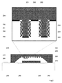
図1では、本発明に係る微小表面構造1の一部が拡大され、概略的に示されている。微小表面構造1は、基板202に接して、または基板202上に形成されている。図1を著しく拡大すると、微小表面構造1の立体200だけが示される。当該立体は、基板面204に対して垂直に隆起している。当該基板面は、図1に矢印で示された方向ならびに図面レベルに対して垂直に延在している。図1からは明らかではないが、立体200は横断面において、基板面204に対して平行に、略円形の横断面を有している。立体200の、基板面204に対して垂直に延在する表面205には、波状構造210が設けられており、当該構造は波の谷206ならびに波の山207から成っている。
In FIG. 1, a part of a
基板表面に塗布される機能材料は、図示された例においては、例えばチタンを含有するゲッタ材料220、230である。ゲッタ材料220、230は、例えば蒸着によって、基板表面に塗布される。ゲッタ原子または金属原子、すなわちゲッタ材料の衝突角αは、図1から明らかである。ゲッタ材料220、230の蒸着の間、当該材料がコーティングされるべき微小部材209は、基板面204に対して垂直な回転軸の周りを回転する。基板面204の直交に対して斜めに形成された衝突角αならびに微小部材209全体の回転によって、基板面204に平行な表面のゲッタ材料の分離が生じる。図示された例では、ゲッタまたはチタン薄層230は立体200上に、ならびにゲッタまたはチタン薄層230は基板202の表面上自体に分離する。立体200の、基板204に垂直に向けられた表面205には、ゲッタ材料またはチタン材料が、衝突角αおよび表面205の間の前記回転、ならびに薄片220の形における微小部材209の回転ゆえに堆積する。この原因となるのは、立体200の表面205の波状構造210である。ゲッタ材料またはチタン材料220、230の入射方向(衝突角α)において、波の山207は、それぞれ入射方向において後続の波の谷206を、衝突するゲッタ原子またはチタン原子から遮蔽する。当該原子は、波の山207の領域においてのみ、ここでは特に波の山207の入射方向211の側に吸着する。成長するゲッタ吸着またはチタン吸着は、入射方向αにおいて後続の領域または波の谷206を継続して遮蔽する。微小部材209の回転ゆえに、衝突する材料は、立体200を取り囲む周方向において一様に分離し、それによって前記ゲッタ薄片またはチタン薄片220が形成される。当該薄片は、斜めの入射角αゆえに、角度βだけ基板面204に対して傾斜している。2つの波の山207の間の間隔ゆえに、薄片220は互いに離間して形成されており、隣の薄片220との間には、間隔240が形成されている。
In the illustrated example, the functional material applied to the substrate surface is, for example,
立体200は、本発明に係る第1の微細構造2を形成し、薄片220は本発明に係る第2の微細構造3を形成する。
The solid 200 forms the first microstructure 2 according to the invention, and the
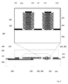
特に図2、図3、図4から明らかなように、微小部材209においては、図1に沿って形成された複数の立体200が、並んで基板202上に配置されている。隣の立体200との間には、やはり空間201が形成されている。図2に示された実施形態においては、立体200は基板202に接して形成されており、当該基板は図示された微小部材209のための蓋部208を形成している。蓋部208を形成する基板202内には、例えば適切なエッチング方法によってくぼみが設けられ、当該くぼみは下部基板280とともに空洞250を形成する。空洞250の底面251には、上述の立体200が配置されており、上述の方法によって、機能材料またはゲッタ220、230がコーティングされる。
As is clear from FIGS. 2, 3, and 4, in the
蓋部208は、封印枠270を間に挟み、下部基板280上に配置されているので、空洞250は周囲に対して密閉されている。下部基板280の蓋部208を向いた側には、1つ以上の微小構造290が配置されている。当該構造は、例えば慣性および回転率センサの振動要素であっても良い。微小構造290によって捕捉される測定値は、従来の方法において測定信号に変換される。当該測定信号は、例示的に示された電気的接続部290を通じて測定される。
Since the
図3には、本発明に係る微小表面を有する微小電気機械部材209のさらなる実施形態が示されている。部材209は、対応する空洞250を有する蓋部208を備えている。当該蓋部は封印枠270を介して、その下に配置された下部基板280と連結されている。当該下部基板は、その蓋部208に対向する表面に、誘電体295がコーティングされている。誘電体295には、やはり電気的ストリップ導体293が、例えば、後続の部分的に腐食した電極金属化の形において塗布された。電気的ストリップ導体293もしくは誘電体295の上方には、さらなる誘電体294が配置されている。当該誘電体は、その下部基板280に対向する側で、封印枠270に連結されている。蓋部208、封印枠270、誘電体294、295、ならびに電気的ストリップ導体293と下部基板280との間の結合はやはり密閉されている。下部基板280と蓋部208との間には空洞250が形成されており、当該空洞内では、微小構造292、例えば対応する運動把握要素を有する回転発振器が、下部基板280に配置されている。さらに、空洞250においては、本発明に係る微小表面構造1の形でゲッタが配置されている。当該微小表面構造は、すでに図1および図2に関連して述べたように、立体200の形での第1の微細構造2、ならびに第2の微細構造3の形での、第1の微細構造2に塗布されたゲッタ材料220、230から成る。微小表面構造201は、下部基板280もしくは当該基板上に塗布された誘電性層295に配置されており、当該誘電性層は、この場合、微小部材として基板202を形成する。
FIG. 3 shows a further embodiment of a micro
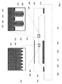
本発明のさらなる第2の実施形態は、図4および図5に、微小赤外線検出器の形で示されている。図4に示された検出器は、下部基板280を有しており、その上面には、一体的な回路296が組み込まれている。さらに、下部基板280は、封印枠270を支持しており、当該封印枠は蓋部208と結合されている。下部基板280、封印枠270、および蓋部208は空洞250を形成し、当該空洞において下部基板280には、光学または赤外線照射による検出または相互作用のために、微小構造297が配置されている。当該空洞250は、蓋部208を形成する基板202内にくぼみがエッチングされることによって形成される。蓋部208のくぼみの底面251内には、立体200ならびに間隔201から成る、図1から図3に関して上述した第1の微細構造2が挿入されている。当該微細構造は、薄層230としての第2の微細構造3の形において、ならびに薄片220の形において、ゲッタがコーティングされている。その側方には、光学ウィンドウ300に対して蓋部208が形成されている。蓋部208の、下部基板280を向いた側には、微小構造化された反射防止層301が設けられており、当該反射防止層は、間隔302だけ互いに離間した立体303から成っている。微小構造化された反射防止層301は、第1の微細構造2と同じように製造される。
A further second embodiment of the invention is shown in FIGS. 4 and 5 in the form of a micro-infrared detector. The detector shown in FIG. 4 has a
蓋部208の、微小構造化された反射防止層301に対向する側には、蓋部208の外側くぼみ320における光学ウィンドウの反射防止のために薄層330が配置されている。
On the side of the
図5に示された微小部材209は、図4に示された微小部材とは、くぼみ320中の薄層330の代わりに、外側に微小構造化された反射防止層310が設けられているという点で異なっている。当該反射防止層は、空洞内に配置された微小構造化された反射防止層301に略一致している。
The
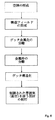
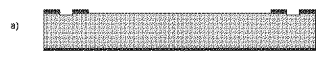
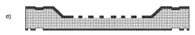
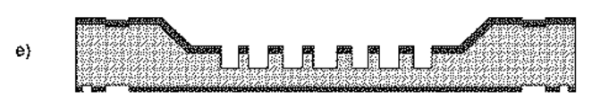
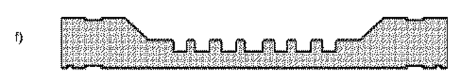
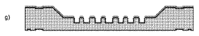
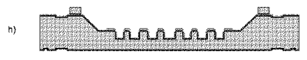
本発明に係る方法の進行を、図6のフローチャートを用いて例示的に示す。対応する製造段階における基板202を図7に示す。当該方法のステップ100では、基板202(図7c)にくぼみが形成され、当該くぼみは微小部材ののちの空洞250を形成する。当該くぼみは、一般的なエッチング方法を用いて、基板内に設けられる。
The progress of the method according to the invention is exemplarily shown using the flowchart of FIG. The
当該方法のステップ110では、構造フィールドが形成される。ここでは、構造フィールドは、立体200および間隔201を有する第1の微細構造2であり、微小構造化された反射防止層301、310でもあると理解される。好ましくは、当該構造フィールドは、例えばCF4、SF6などの反応性ガスを用いた異方性乾式エッチング方法によって形成される(図7c、7d)。
In step 110 of the method, a structure field is formed. Here, the structural field is understood to be the first microstructure 2 having the solid 200 and the
続いて、当該方法のステップ120では、ゲッタの金属化が分離する。当該金属化は、特に第1の微細構造(200、201)に、薄層230ならびに薄片220の形で分離する(図7g)。
Subsequently, in step 120 of the method, getter metallization is separated. The metallization separates into the first microstructure (200, 201) in the form of a
当該方法のステップ130では、金属枠が分離し、当該金属枠はのちの封印枠270を形成する。金属枠の分離は、好ましくは、例えば金または金/スズめっきの塗布によって行われる(図7h)。
In step 130 of the method, the metal frame separates and the metal frame later forms a
続く当該方法のステップ140では、ゲッタの構造化が行われる。このとき、塗布されたゲッタ材料の横の境界が、例えばリフトオフ構造化によって決定される(図7g、図7h)。同様に、維持すべきゲッタ構造を覆うためのフォトレジストを有する標準リソグラフィと、露出したゲッタ材料の後続の構造化とが行われる。当該構造化は、ゲッタ材料に応じて、湿式化学的または乾式的に、すなわち反応ガス(チタンおよびジルコンの場合は、例えばHF、HF含有エッチング)によって行われる。 In the subsequent step 140 of the method, getter structuring is performed. At this time, the lateral boundaries of the applied getter material are determined, for example, by lift-off structuring (FIGS. 7g, 7h). Similarly, standard lithography with a photoresist to cover the getter structure to be maintained and subsequent structuring of the exposed getter material is performed. Depending on the getter material, the structuring is carried out wet-chemically or dryly, ie with a reactive gas (for example titanium or zircon, for example HF, HF-containing etching).
最後に、当該方法のステップ150では、部材の封鎖が、下部基板280、封印枠270、および蓋部208間の接着によって行われる。部材の封印は、制御された雰囲気(真空)下で行われる。
Finally, in step 150 of the method, the member is sealed by bonding between the
α 衝突角
β ゲッタまたはチタン薄片の配置角度
1 微小表面構造
2 第1の微細構造
3 第2の微細構造
100‐150 プロセスフロー
200 立体
201 空間
202 基板
203 ゲッタ構造を有する領域
204 基板面
205 立体200の表面
206 波の谷
207 波の山
208 蓋部
209 微小部材
210 波構造
220 ゲッタまたはチタン薄片
230 ゲッタまたはチタン薄層
240 間隔
250 空洞
251 底面
270 封印枠
280 下部基板
290 微小構造
291 電気的接続部
292 微小構造
293 電気的ストリップ導体
294 誘電体
295 誘電体
296 一体的な回路
297 光学または赤外線照射による検出または相互作用のための微小構造
300 空洞内の光学ウィンドウ
301 微小構造化された反射防止層
302 反射防止層の間隔と深さ
303 立体
310 外側の光学ウィンドウ
320 外側の光学ウィンドウのくぼみ
330 光学ウィンドウの反射防止のための薄層
α Collision angle β Getter or titanium
Claims (17)
前記第1の微細構造の前記第1の隆起および/またはくぼみは、機能材料がコーティングされるべき表面を有しており、
前記表面は、基板面に対して略垂直または斜めに延在しており、
前記第1の微細構造の前記機能材料がコーティングされるべき表面は、少なくとも領域的に第2の波状またはこぶ状隆起および/またはくぼみを有しており、
前記コーティングされるべき表面の、前記第2のこぶ状または波状隆起および/またはくぼみは、核形成点として用いられ、前記核形成点には前記機能材料が好ましくは分離し、
前記機能材料は、前記コーティングされるべき表面から隆起した立体を有する第2の微細構造の形で、好ましくは薄片および/または棒の形で塗布されることを特徴とする方法。 A method for forming a micro-surface structure on a substrate, in particular a method for manufacturing a micro-electromechanical member, comprising at least a first ridge and / or indentation, in particular a number of first ridges, on or in the substrate. In the method in which the first microstructure with the depression is formed,
The first ridge and / or indentation of the first microstructure has a surface on which a functional material is to be coated;
The surface extends substantially perpendicularly or obliquely to the substrate surface;
The surface to which the functional material of the first microstructure is to be coated has at least regionally a second wavy or hump ridge and / or indentation;
The second hump or wavy ridge and / or indentation of the surface to be coated is used as a nucleation point, where the functional material preferably separates,
Method according to claim 1, characterized in that the functional material is applied in the form of a second microstructure having a solid raised from the surface to be coated, preferably in the form of flakes and / or bars.
基板上または基板内には、少なくとも1つの第1の隆起および/またはくぼみ、特に多数の第1の隆起および/またはくぼみ、および基板面に対して略垂直または斜めの表面を有する第1の微細構造が設けられており、
第1の隆起および/またはくぼみの、前記基板面に対して略垂直または斜めの表面は、少なくとも領域的に、波状またはこぶ状の第2の隆起および/またはくぼみを有しており、
前記第1の隆起および/またはくぼみの、前記基板面に対して略垂直または斜めの表面には、機能材料が配置されており、
前記機能材料は、前記第1の隆起および/またはくぼみの表面から隆起した立体を有する第2の微細構造の形において、特に薄片または棒の形において形成されている
ことを特徴とする微小表面構造。 Especially in a micro-surface structure produced by the method according to any one of claims 1 to 9,
A first fine having at least one first ridge and / or depression, in particular a large number of first ridges and / or depressions, and a surface substantially perpendicular or oblique to the substrate surface, on or in the substrate Structure is provided,
The surface of the first ridge and / or indentation that is substantially perpendicular or oblique to the substrate surface has at least in part a wavy or bumpy second ridge and / or indentation;
A functional material is disposed on a surface of the first ridge and / or indentation that is substantially perpendicular or oblique to the substrate surface;
The micro-surface structure characterized in that the functional material is formed in the form of a second microstructure having a solid raised from the surface of the first ridge and / or indentation, in particular in the form of a flake or rod .
赤外線照射のための反射防止構造を備えたウィンドウ領域が設けられていること、
前記反射防止構造は、好ましくは基板面に対して略垂直な表面を有する、多数の、特にマトリックス状に配置された隆起および/またはくぼみを有しており、前記基板内に形成された空洞内に配置されていることを特徴とする請求項14に記載の微小電気機械部材。 The microelectromechanical member according to claim 14,
A window region with an antireflection structure for infrared irradiation is provided,
The antireflective structure has a number of ridges and / or indentations arranged in a matrix, preferably having a surface substantially perpendicular to the substrate surface, in a cavity formed in the substrate The microelectromechanical member according to claim 14, wherein the microelectromechanical member is disposed on the surface.
反射防止コーティングが少なくとも1つの薄層から、好ましくはそれぞれ4つの交互のSi‐ZnS層から成ること、
前記反射防止コーティングは、前記基板の部材内側および/または部材外側を向いた側に配置されていることを特徴とする請求項14または15に記載の微小電気機械部材。 The microelectromechanical member according to claim 14 or 15,
The antireflective coating consists of at least one thin layer, preferably each of four alternating Si-ZnS layers;
16. The microelectromechanical member according to claim 14, wherein the antireflection coating is disposed on a side of the substrate facing the member inner side and / or the member outer side.
少なくとも1つの反射防止コーティングが、少なくとも1つの隆起および/またはくぼみ、特に多数の隆起および/またはくぼみ、および基板面に対して略垂直または斜めの表面を有する第1の微細構造を有しており、隣接する隆起もしくはくぼみは、互いに好ましくは3μm〜40μm、より好ましくは4μmの中心間間隔を有し、および/または前記隆起もしくはくぼみは、好ましくは50μmよりも少ない、より好ましくは10μm〜20μmの高さもしくは深さを有していることを特徴とする請求項16に記載の微小電気機械部材。 The microelectromechanical member according to claim 16,
The at least one anti-reflective coating has a first microstructure having at least one ridge and / or indentation, in particular a large number of ridges and / or indentations, and a surface substantially perpendicular or oblique to the substrate surface; Adjacent ridges or depressions preferably have a center-to-center spacing of 3 μm to 40 μm, more preferably 4 μm, and / or said ridges or depressions are preferably less than 50 μm, more preferably 10 μm to 20 μm. The microelectromechanical member according to claim 16, which has a height or a depth.
Applications Claiming Priority (5)
| Application Number | Priority Date | Filing Date | Title |
|---|---|---|---|
| DE102008057858.4 | 2008-11-18 | ||
| DE102008057858 | 2008-11-18 | ||
| DE102008060796.7 | 2008-12-05 | ||
| DE102008060796.7A DE102008060796B4 (en) | 2008-11-18 | 2008-12-05 | Method for forming a micro-surface structure and for producing a micro-electro-mechanical component, micro-surface structure and microelectromechanical component having such a structure |
| PCT/EP2009/065293 WO2010057878A2 (en) | 2008-11-18 | 2009-11-17 | Method for forming a micro-surface structure and for producing a micro-electromechanical component, micro-surface structure and micro-electromechanical component having said micro-surface structure |
Publications (2)
| Publication Number | Publication Date |
|---|---|
| JP2012509201A true JP2012509201A (en) | 2012-04-19 |
| JP5701773B2 JP5701773B2 (en) | 2015-04-15 |
Family
ID=42105264
Family Applications (1)
| Application Number | Title | Priority Date | Filing Date |
|---|---|---|---|
| JP2011543766A Expired - Fee Related JP5701773B2 (en) | 2008-11-18 | 2009-11-17 | Method for forming micro surface structure, method for manufacturing micro electro mechanical member, micro surface structure, and micro electro mechanical member having the structure |
Country Status (4)
| Country | Link |
|---|---|
| US (1) | US9637377B2 (en) |
| JP (1) | JP5701773B2 (en) |
| DE (1) | DE102008060796B4 (en) |
| WO (1) | WO2010057878A2 (en) |
Cited By (2)
| Publication number | Priority date | Publication date | Assignee | Title |
|---|---|---|---|---|
| KR20160090367A (en) * | 2014-02-28 | 2016-07-29 | 레이던 컴퍼니 | Getter structure and method for forming such structure |
| JP2019174271A (en) * | 2018-03-28 | 2019-10-10 | セイコーインスツル株式会社 | Infrared sensor and manufacturing method for infrared sensor |
Families Citing this family (7)
| Publication number | Priority date | Publication date | Assignee | Title |
|---|---|---|---|---|
| EP2264765A1 (en) | 2009-06-19 | 2010-12-22 | Fraunhofer-Gesellschaft zur Förderung der angewandten Forschung e.V. | Housing for an infrared radiation micro device and method for fabricating such housing |
| DE102012216618A1 (en) | 2012-09-18 | 2014-03-20 | Robert Bosch Gmbh | Arrangement of at least two wafers for detecting electromagnetic radiation and method for producing the arrangement |
| US20140175590A1 (en) * | 2012-12-20 | 2014-06-26 | Raytheon Company | Getter structure for wafer level vacuum packaged device |
| US9511998B2 (en) | 2013-03-13 | 2016-12-06 | Robert Bosch Gmbh | MEMS device having a getter |
| FR3014241B1 (en) * | 2013-11-29 | 2017-05-05 | Commissariat Energie Atomique | ENCAPSULATION STRUCTURE COMPRISING PARTIALLY FILLED TRENCHES OF MATERIAL GETTER |
| FR3014240B1 (en) * | 2013-11-29 | 2017-05-05 | Commissariat Energie Atomique | METHOD FOR PRODUCING A SUBSTRATE HAVING GETTER MATERIAL ARRANGED ON WALLS OF ONE OR MORE BORGED HOLES FORMED IN THE SUBSTRATE |
| FR3109936B1 (en) | 2020-05-07 | 2022-08-05 | Lynred | METHOD FOR MANUFACTURING AN ELECTROMECHANICAL MICROSYSTEM AND ELECTROMECHANICAL MICROSYSTEM |
Citations (7)
| Publication number | Priority date | Publication date | Assignee | Title |
|---|---|---|---|---|
| JP2000057940A (en) * | 1998-08-10 | 2000-02-25 | Yamaha Corp | Electric-field-emission-type element and its manufacture |
| JP2002352700A (en) * | 2001-04-16 | 2002-12-06 | Hewlett Packard Co <Hp> | Electronic device equipped with getter and its operation method |
| JP2006501679A (en) * | 2002-09-30 | 2006-01-12 | モトローラ・インコーポレイテッド | Hermetically sealed microdevice with single crystal silicon getter to maintain vacuum |
| JP2007523467A (en) * | 2003-11-14 | 2007-08-16 | サエス・ゲッタース・ソチエタ・ペル・アツィオニ | Method of manufacturing a device that requires a non-volatile getter material for operation |
| JP2007291529A (en) * | 2001-03-13 | 2007-11-08 | Kiyousera Opt Kk | Metal film-coated member and method for producing the same |
| JP2007316005A (en) * | 2006-05-29 | 2007-12-06 | Nissan Motor Co Ltd | Infrared sensor and manufacturing method therefor |
| JP2008135690A (en) * | 2006-10-30 | 2008-06-12 | Denso Corp | Semiconductor physical quantity sensor and method of manufacturing same |
Family Cites Families (12)
| Publication number | Priority date | Publication date | Assignee | Title |
|---|---|---|---|---|
| US4769345A (en) * | 1987-03-12 | 1988-09-06 | Olin Corporation | Process for producing a hermetically sealed package for an electrical component containing a low amount of oxygen and water vapor |
| US5701008A (en) * | 1996-11-29 | 1997-12-23 | He Holdings, Inc. | Integrated infrared microlens and gas molecule getter grating in a vacuum package |
| US6346455B1 (en) * | 2000-08-31 | 2002-02-12 | Micron Technology, Inc. | Method to form a corrugated structure for enhanced capacitance |
| US6923625B2 (en) * | 2002-01-07 | 2005-08-02 | Integrated Sensing Systems, Inc. | Method of forming a reactive material and article formed thereby |
| US6958846B2 (en) * | 2002-11-26 | 2005-10-25 | Reflectivity, Inc | Spatial light modulators with light absorbing areas |
| US6988924B2 (en) * | 2003-04-14 | 2006-01-24 | Hewlett-Packard Development Company, L.P. | Method of making a getter structure |
| ITMI20031178A1 (en) | 2003-06-11 | 2004-12-12 | Getters Spa | MULTILAYER NON-EVAPORABLE GETTER DEPOSITS OBTAINED FOR |
| US7115436B2 (en) | 2004-02-12 | 2006-10-03 | Robert Bosch Gmbh | Integrated getter area for wafer level encapsulated microelectromechanical systems |
| US7211881B2 (en) * | 2004-03-24 | 2007-05-01 | Hewlett-Packard Development Company, L.P. | Structure for containing desiccant |
| US20060076634A1 (en) | 2004-09-27 | 2006-04-13 | Lauren Palmateer | Method and system for packaging MEMS devices with incorporated getter |
| US7147908B2 (en) * | 2004-10-13 | 2006-12-12 | Hewlett-Packard Development Company, L.P. | Semiconductor package with getter formed over an irregular structure |
| US7462931B2 (en) * | 2006-05-15 | 2008-12-09 | Innovative Micro Technology | Indented structure for encapsulated devices and method of manufacture |
-
2008
- 2008-12-05 DE DE102008060796.7A patent/DE102008060796B4/en active Active
-
2009
- 2009-11-17 JP JP2011543766A patent/JP5701773B2/en not_active Expired - Fee Related
- 2009-11-17 WO PCT/EP2009/065293 patent/WO2010057878A2/en active Application Filing
- 2009-11-17 US US13/129,601 patent/US9637377B2/en active Active
Patent Citations (7)
| Publication number | Priority date | Publication date | Assignee | Title |
|---|---|---|---|---|
| JP2000057940A (en) * | 1998-08-10 | 2000-02-25 | Yamaha Corp | Electric-field-emission-type element and its manufacture |
| JP2007291529A (en) * | 2001-03-13 | 2007-11-08 | Kiyousera Opt Kk | Metal film-coated member and method for producing the same |
| JP2002352700A (en) * | 2001-04-16 | 2002-12-06 | Hewlett Packard Co <Hp> | Electronic device equipped with getter and its operation method |
| JP2006501679A (en) * | 2002-09-30 | 2006-01-12 | モトローラ・インコーポレイテッド | Hermetically sealed microdevice with single crystal silicon getter to maintain vacuum |
| JP2007523467A (en) * | 2003-11-14 | 2007-08-16 | サエス・ゲッタース・ソチエタ・ペル・アツィオニ | Method of manufacturing a device that requires a non-volatile getter material for operation |
| JP2007316005A (en) * | 2006-05-29 | 2007-12-06 | Nissan Motor Co Ltd | Infrared sensor and manufacturing method therefor |
| JP2008135690A (en) * | 2006-10-30 | 2008-06-12 | Denso Corp | Semiconductor physical quantity sensor and method of manufacturing same |
Non-Patent Citations (1)
| Title |
|---|
| JPN7013004020; KOSTOVSKI G; MITCHELL A; HOLLAND A; AUSTIN M: 'Sidewall corrugation lithography: bulk fabrication of ordered nanowires, nanoribbons, and nanorings' APPLIED PHYSICS LETTERS vol.92,no.22, 20080604, 223109-1-223109-3, AMERICAN INSTITUTE OF PHYSICS, USA * |
Cited By (8)
| Publication number | Priority date | Publication date | Assignee | Title |
|---|---|---|---|---|
| KR20160090367A (en) * | 2014-02-28 | 2016-07-29 | 레이던 컴퍼니 | Getter structure and method for forming such structure |
| JP2017506835A (en) * | 2014-02-28 | 2017-03-09 | レイセオン カンパニー | Getter structure and method of forming the structure |
| KR20180091954A (en) * | 2014-02-28 | 2018-08-16 | 레이던 컴퍼니 | Getter structure and method for forming getter structure |
| KR101891011B1 (en) * | 2014-02-28 | 2018-08-22 | 레이던 컴퍼니 | Getter structure and method for forming such structure |
| JP2019047125A (en) * | 2014-02-28 | 2019-03-22 | レイセオン カンパニー | Getter structure and method for forming that structure |
| KR101993107B1 (en) | 2014-02-28 | 2019-06-25 | 레이던 컴퍼니 | Getter structure and method for forming getter structure |
| JP2019174271A (en) * | 2018-03-28 | 2019-10-10 | セイコーインスツル株式会社 | Infrared sensor and manufacturing method for infrared sensor |
| JP7112866B2 (en) | 2018-03-28 | 2022-08-04 | セイコーインスツル株式会社 | Infrared sensor and method for manufacturing infrared sensor |
Also Published As
| Publication number | Publication date |
|---|---|
| DE102008060796B4 (en) | 2014-01-16 |
| WO2010057878A3 (en) | 2011-02-24 |
| WO2010057878A2 (en) | 2010-05-27 |
| US20110287214A1 (en) | 2011-11-24 |
| US9637377B2 (en) | 2017-05-02 |
| DE102008060796A1 (en) | 2010-05-20 |
| JP5701773B2 (en) | 2015-04-15 |
Similar Documents
| Publication | Publication Date | Title |
|---|---|---|
| JP5701773B2 (en) | Method for forming micro surface structure, method for manufacturing micro electro mechanical member, micro surface structure, and micro electro mechanical member having the structure | |
| US7462931B2 (en) | Indented structure for encapsulated devices and method of manufacture | |
| US6806557B2 (en) | Hermetically sealed microdevices having a single crystalline silicon getter for maintaining vacuum | |
| JP6140259B2 (en) | Support for microelectronics, microoptoelectronics or micromechanics devices | |
| US6923625B2 (en) | Method of forming a reactive material and article formed thereby | |
| US7732902B2 (en) | Semiconductor package with getter formed over an irregular structure | |
| US20090001537A1 (en) | Gettering material for encapsulated microdevices and method of manufacture | |
| WO2009087284A1 (en) | Structure comprising a getter layer and an adjusting sublayer, and fabrication process | |
| JP4831931B2 (en) | Support with integrated deposits of gas-absorbing material for the production of microelectronic, microoptoelectronic or micromechanical devices | |
| EP2537797B1 (en) | Structure with getter material hermetically protected during the manufacturing thereof | |
| CN105236345A (en) | MEMS (Micro Electro Mechanical System) device, semiconductor device and manufacturing methods thereof | |
| Sparks et al. | Reliable vacuum packaging using nanogetters and glass frit bonding | |
| Anderson et al. | 14 Advances in WLCSP Technologies for Growing Market Needs | |
| US11685645B2 (en) | Micro-electromechanical system and method for producing same | |
| US8912620B2 (en) | Getter structure with optimized pumping capacity | |
| EP3034460B1 (en) | Multi-level getter structure and encapsulation structure comprising such a multi-level getter structure | |
| JP7404558B2 (en) | MEMS hermetic sealing device and method | |
| CN112930318A (en) | Hermetic housing comprising a getter, optoelectronic component or MEMS device incorporating such a hermetic housing, and related manufacturing method |
Legal Events
| Date | Code | Title | Description |
|---|---|---|---|
| A621 | Written request for application examination |
Free format text: JAPANESE INTERMEDIATE CODE: A621 Effective date: 20120828 |
|
| A977 | Report on retrieval |
Free format text: JAPANESE INTERMEDIATE CODE: A971007 Effective date: 20131031 |
|
| A601 | Written request for extension of time |
Free format text: JAPANESE INTERMEDIATE CODE: A601 Effective date: 20140205 |
|
| A602 | Written permission of extension of time |
Free format text: JAPANESE INTERMEDIATE CODE: A602 Effective date: 20140213 |
|
| A521 | Request for written amendment filed |
Free format text: JAPANESE INTERMEDIATE CODE: A523 Effective date: 20140411 |
|
| A02 | Decision of refusal |
Free format text: JAPANESE INTERMEDIATE CODE: A02 Effective date: 20140722 |
|
| A521 | Request for written amendment filed |
Free format text: JAPANESE INTERMEDIATE CODE: A523 Effective date: 20141125 |
|
| A911 | Transfer to examiner for re-examination before appeal (zenchi) |
Free format text: JAPANESE INTERMEDIATE CODE: A911 Effective date: 20141202 |
|
| TRDD | Decision of grant or rejection written | ||
| A01 | Written decision to grant a patent or to grant a registration (utility model) |
Free format text: JAPANESE INTERMEDIATE CODE: A01 Effective date: 20150119 |
|
| A61 | First payment of annual fees (during grant procedure) |
Free format text: JAPANESE INTERMEDIATE CODE: A61 Effective date: 20150218 |
|
| R150 | Certificate of patent or registration of utility model |
Ref document number: 5701773 Country of ref document: JP Free format text: JAPANESE INTERMEDIATE CODE: R150 |
|
| R250 | Receipt of annual fees |
Free format text: JAPANESE INTERMEDIATE CODE: R250 |
|
| R250 | Receipt of annual fees |
Free format text: JAPANESE INTERMEDIATE CODE: R250 |
|
| R250 | Receipt of annual fees |
Free format text: JAPANESE INTERMEDIATE CODE: R250 |
|
| LAPS | Cancellation because of no payment of annual fees |