JP2012507781A - Computer bus with configurable configuration - Google Patents
Computer bus with configurable configuration Download PDFInfo
- Publication number
- JP2012507781A JP2012507781A JP2011534461A JP2011534461A JP2012507781A JP 2012507781 A JP2012507781 A JP 2012507781A JP 2011534461 A JP2011534461 A JP 2011534461A JP 2011534461 A JP2011534461 A JP 2011534461A JP 2012507781 A JP2012507781 A JP 2012507781A
- Authority
- JP
- Japan
- Prior art keywords
- bus
- coupled
- optoelectronic
- electronic device
- flexible
- Prior art date
- Legal status (The legal status is an assumption and is not a legal conclusion. Google has not performed a legal analysis and makes no representation as to the accuracy of the status listed.)
- Granted
Links
- 230000005693 optoelectronics Effects 0.000 claims abstract description 42
- 230000003287 optical effect Effects 0.000 claims description 14
- 229910052751 metal Inorganic materials 0.000 claims description 5
- 239000002184 metal Substances 0.000 claims description 5
- 239000013307 optical fiber Substances 0.000 claims description 3
- 230000008878 coupling Effects 0.000 claims 2
- 238000010168 coupling process Methods 0.000 claims 2
- 238000005859 coupling reaction Methods 0.000 claims 2
- 229920001971 elastomer Polymers 0.000 claims 1
- 239000000806 elastomer Substances 0.000 claims 1
- WABPQHHGFIMREM-UHFFFAOYSA-N lead(0) Chemical compound [Pb] WABPQHHGFIMREM-UHFFFAOYSA-N 0.000 claims 1
- 238000004891 communication Methods 0.000 description 8
- 230000005540 biological transmission Effects 0.000 description 3
- 238000012986 modification Methods 0.000 description 3
- 230000004048 modification Effects 0.000 description 3
- 238000003491 array Methods 0.000 description 2
- 239000004020 conductor Substances 0.000 description 2
- 230000007423 decrease Effects 0.000 description 2
- 230000002093 peripheral effect Effects 0.000 description 2
- 239000004642 Polyimide Substances 0.000 description 1
- BQCADISMDOOEFD-UHFFFAOYSA-N Silver Chemical compound [Ag] BQCADISMDOOEFD-UHFFFAOYSA-N 0.000 description 1
- 230000000295 complement effect Effects 0.000 description 1
- 238000005516 engineering process Methods 0.000 description 1
- 230000006870 function Effects 0.000 description 1
- 230000002452 interceptive effect Effects 0.000 description 1
- 239000004033 plastic Substances 0.000 description 1
- 150000003071 polychlorinated biphenyls Chemical class 0.000 description 1
- 229920000728 polyester Polymers 0.000 description 1
- 229920001721 polyimide Polymers 0.000 description 1
- 229910052709 silver Inorganic materials 0.000 description 1
- 239000004332 silver Substances 0.000 description 1
- 239000000758 substrate Substances 0.000 description 1
Images


Classifications
-
- G—PHYSICS
- G06—COMPUTING; CALCULATING OR COUNTING
- G06F—ELECTRIC DIGITAL DATA PROCESSING
- G06F13/00—Interconnection of, or transfer of information or other signals between, memories, input/output devices or central processing units
- G06F13/38—Information transfer, e.g. on bus
- G06F13/40—Bus structure
-
- G—PHYSICS
- G02—OPTICS
- G02B—OPTICAL ELEMENTS, SYSTEMS OR APPARATUS
- G02B6/00—Light guides; Structural details of arrangements comprising light guides and other optical elements, e.g. couplings
- G02B6/24—Coupling light guides
- G02B6/42—Coupling light guides with opto-electronic elements
- G02B6/43—Arrangements comprising a plurality of opto-electronic elements and associated optical interconnections
-
- G—PHYSICS
- G06—COMPUTING; CALCULATING OR COUNTING
- G06F—ELECTRIC DIGITAL DATA PROCESSING
- G06F1/00—Details not covered by groups G06F3/00 - G06F13/00 and G06F21/00
- G06F1/16—Constructional details or arrangements
- G06F1/18—Packaging or power distribution
- G06F1/183—Internal mounting support structures, e.g. for printed circuit boards, internal connecting means
Abstract
本発明の種々の実施形態は、種々のコンピュータシステムのコンポーネント間でデータを配送するために使用可能なコンピュータバスに向けられている。1側面では、コンピュータバス(100)は、ハウジング(102)内に配置された複数の光電子エンジン(104-112)、及び複数のフレキシブルコネクタ(116-124)を備える。フレキシブルコネクタの各々は開口部を通ってハウジング内に延在し、第1の端部で光電子エンジンに結合し、第2の端部で電子装置に結合する。フレキシブルコネクタは、空間及び接続性の要件または制限を最適化するために、バスを異なる向き及び位置に配置することができる。Various embodiments of the present invention are directed to a computer bus that can be used to distribute data between components of various computer systems. In one aspect, the computer bus (100) includes a plurality of optoelectronic engines (104-112) and a plurality of flexible connectors (116-124) disposed within the housing (102). Each flexible connector extends through the opening into the housing and is coupled to the optoelectronic engine at a first end and to an electronic device at a second end. Flexible connectors can arrange the buses in different orientations and locations to optimize space and connectivity requirements or limitations.
Description
本発明の実施形態は、一般的にはコンピュータバスに関連し、特に、特定の用途毎に異なる向きで配置することが可能なコンピュータバスに関連する。 Embodiments of the present invention relate generally to computer buses, and more particularly to computer buses that can be arranged in different orientations for specific applications.
コンピュータアーキテクチャにおいて、バスは、単一のコンピュータのコンピュータコンポーネント間、または、コンピュータ間でデータを伝送するためのサブシステムである。ポイントツーポイント接続とは異なり、バスは、同じ組をなす信号線を介して、いくつかの周辺装置を論理的に接続する。換言すれば、各バスは、典型的には、CPU及びメモリなどの装置を電子的に接続する一組の信号線から構成される。バスには、アドレスバスとデータバスが含まれる。データバスはデータを伝送し、アドレスバスは、データの物理的な位置及びデータの宛先の位置に関する情報を伝送する。バスをパラレスバスまたはシリアルバスとすることができ、パラレルバスは、複数の信号線上を同時に(または並列に)データワードを伝送し、シリアルバスは、ビットシリアル形態でデータを伝送する。ほとんどのコンピュータは内部バスと外部バスの両方を有している。内部バスは、回路基板に印刷された1組の信号線から構成される。内部バスは、コンピュータの内部コンポーネントを接続する。一方、外部バスは、外部の周辺装置を回路基板に接続する。 In a computer architecture, a bus is a subsystem for transmitting data between computer components of a single computer or between computers. Unlike point-to-point connections, the bus logically connects several peripheral devices via the same set of signal lines. In other words, each bus is typically composed of a set of signal lines that electronically connect devices such as a CPU and a memory. The bus includes an address bus and a data bus. The data bus carries data, and the address bus carries information about the physical location of the data and the location of the data destination. The bus can be a parallel bus or a serial bus, the parallel bus transmits data words simultaneously (or in parallel) on a plurality of signal lines, and the serial bus transmits data in bit serial form. Most computers have both an internal bus and an external bus. The internal bus is composed of a set of signal lines printed on a circuit board. The internal bus connects the internal components of the computer. On the other hand, the external bus connects an external peripheral device to the circuit board.
近年、集積回路(「IC」)技術の開発はコンピュータコンポーネントのサイズを小さくする点で著しく進歩しており、これによって、コンポーネントの密度が増加し、信号線の断面の寸法が減少し、及び、より小さな表面積に信号線が詰め込まれるようになってきた。その結果、従来の金属信号線は、それらの情報伝送能力の本質的な物理的限界に近づいている。さらに、プリント回路のバス経路を横断するのに必要な相対的な時間が非常に長くなっているので、より小さなコンポーネントによってもたらされる高速性能の利点を十分に活用できない。換言すれば、データレート(またはデータ転送速度)が高くなると、信号線の情報伝送能力は、信号線のサイズの減少とともに低下し、間隔が狭い信号線は、干渉すなわちクロストークを生ずることなしには高速信号を伝送することはできない。 In recent years, the development of integrated circuit (“IC”) technology has made significant progress in reducing the size of computer components, which increases the density of components, reduces the cross-sectional dimensions of signal lines, and Signal lines have been packed into smaller surface areas. As a result, conventional metal signal lines are approaching the essential physical limits of their information transmission capabilities. Furthermore, the relative time required to traverse the printed circuit bus path is so long that the high speed performance benefits provided by smaller components cannot be fully exploited. In other words, as the data rate (or data transfer rate) increases, the information transmission capability of the signal line decreases with a decrease in the size of the signal line, and a signal line having a narrow interval does not cause interference, that is, crosstalk. Cannot transmit high-speed signals.
したがって、コンピューティング装置の製造者、設計者、及びユーザは、現在利用されているバスに本質的に存在する表面積及び信号速度の制約を受けることなく、ICコンポーネント間にデータを配送するための高速バスに対する需要があることを認識している。 Thus, manufacturers, designers, and users of computing devices are able to deliver high-speed data delivery between IC components without the surface area and signal speed constraints inherent in presently used buses. Recognize that there is a demand for buses.
本発明の種々の実施形態は、種々のコンピュータシステムのコンポーネント間にデータを配送するために使用可能なコンピュータバスに向けられている。1側面では、コンピュータバスは、ハウジング(筐体など)内に配置された複数の光電子エンジン及び複数のフレキシブルコネクタ(すなわち折り曲げ可能なコネクタ)を備える。フレキシブルコネクタの各々は、ハウジング内の穴を通り抜け、第1の端部で光電子エンジンに結合され、第2の端部で電子装置(または電子デバイス)に結合される。空間及び接続性に関する要件または制限を最適化するために、フレキシブルコネクタを用いて、バスを、種々の方向に向けて配置し、かつ、種々の位置に配置することができる。フレキシブルコネクタ以外の形成された金属トレース(金属パターン)や弾性導体(またはエラストマー導体)などのコンポーネントが、OEエンジン(光電子エンジン)と二次的な電気装置との間の電気的接続を提供できることもまた事実である。 Various embodiments of the present invention are directed to a computer bus that can be used to distribute data between various computer system components. In one aspect, the computer bus includes a plurality of optoelectronic engines and a plurality of flexible connectors (ie, foldable connectors) disposed within a housing (such as a housing). Each flexible connector passes through a hole in the housing, is coupled to the optoelectronic engine at a first end, and is coupled to an electronic device (or electronic device) at a second end. In order to optimize space or connectivity requirements or restrictions, the flexible connector can be used to place the bus in various directions and in various positions. Components other than flexible connectors, such as formed metal traces (metal patterns) and elastic conductors (or elastomeric conductors), can also provide electrical connections between OE engines (optoelectronic engines) and secondary electrical devices It is also true.
本発明の種々の実施形態は、各々のコンピュータシステムが異なるコンポーネント構成を有する種々のコンピュータシステムのコンポーネント間でデータを配送するために使用可能なコンピュータバスに向けられている。コンピュータシステムを、プリント回路基板(「PCB」)を有するコンピュータ、または、複数のサーバーブレードを有するブレードサーバー、または、多くの通信装置からなる他の任意のシステムとすることができる。PCBを、マザーボード、ミッドプレーン(midplane)、バックプレーン、または、任意のタイプのPCBとすることができる。具体的には、バスは、ほんのいくつかの例を挙げると、複数のプロセッサ間、プロセッサとメモリ間、サーバーブレード間でデータを伝送することができる。いくつかのバスの実施形態は、空間及び接続性の要件または制限を最適化するために種々の異なる位置にバスを向けることができる柔軟な(すなわち折り曲げ可能な)接続を通じてPCBまたはPCB上のコンポーネントに結合される個別のコンポーネントである。換言すれば、バスは、利用可能な空間においてバスを種々の方向に向けることができ、かつ、種々の位置に配置することが可能な柔軟な接続でもってコンピュータシステムに接続される。 Various embodiments of the present invention are directed to a computer bus that can be used to distribute data between components of various computer systems, each computer system having a different component configuration. The computer system can be a computer having a printed circuit board ("PCB"), a blade server having multiple server blades, or any other system of many communication devices. The PCB can be a motherboard, a midplane, a backplane, or any type of PCB. Specifically, the bus can carry data between multiple processors, between processors and memory, and between server blades, to name just a few examples. Some bus embodiments are components on a PCB or PCB through flexible (ie foldable) connections that can direct the bus to a variety of different locations to optimize space and connectivity requirements or limitations Is a separate component that is bound to In other words, the bus is connected to the computer system with a flexible connection that can direct the bus in various directions in the available space and can be placed in various locations.
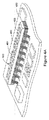
図1A及び図1Bは、本発明の実施形態にしたがって構成されたバス100のそれぞれ異なる等角図である。バス100は、ハウジング102、9つの光電子エンジン104〜112、及び、9つの実質的に同じ構成を有する柔軟な(または可撓性の)電気フレキシブルコネクタ116〜124を備える。ハウジングは、開口部(孔)を有し、フレキシブルコネクタの各々はこの穴を介してハウジング102を通り抜けて、1つの光電子エンジンに電子的に結合される。パッド126などの電気コンタクトパッド(または導電パッド)が、各フレキシブルコネクタの端部に配置されている。図1Bに示すように、個別のフレキシブルコネクタは柔軟であり、各フレキシブルコネクタを、任意の数の異なる構成をなすように別々に曲げることができる。図1Bは、フレキシブルコネクタ119の拡大部128を含んでいる。線130などの線は、パッド126を光電子エンジン107に接続するフレキシブルコネクタ119のそれぞれの印刷された信号線を表している。各フレキシブルコネクタは、パッドからの電気信号を、電子的に結合された光電子エンジンに伝達するために設けられた1組の入力信号線と、電子的に結合された光電子エンジンからの電気信号をパッドに送るために設けられた1組の出力信号線を備える。ハウジング102内において、光電子エンジン104〜112を、光ファイバー、導波路、中空の金属導波路、または、自由空間を介して光学的に結合することができる。図1Bはまた、パッド134の底部に配置されたオスコネクタピンが見えるように向けられたパッド134の拡大部132を含んでいる。オスコネクタピンを、PCBに配置されたメスコネクタの受け口に挿入することができる。各コネクタピンは、電気信号を、フレキシブルコネクタ121中の信号線の1つに送る。PCBに配置されたメスコネクタの各受け口は、該PCBに印刷された信号線に電気的に接続されている。他の実施形態では、パッド134をメスコネクタとして構成することができ、オスコネクタをPCBに配置することができる。さらに他の実施形態では、パッドをPCB上のコネクタにしっかりと固定する留め具を有するように、該パッドを構成することもできる。
1A and 1B are different isometric views of a
いくつかの実施形態では、フレキシブルコネクタをフレックス回路(flex circuit:可撓性の回路)とすることができる。フレキシブルコネクタは、フレキシブル回路基板としても知られているフレキシブルな電子部品の1つのタイプであって、ポリイミドなどの可撓性を有する高性能なプラスチック基板に電子部品を搭載することによって電子回路を組み立てるために使用されることができるものである。さらに、フレックス回路を、ポリエステル上のスクリーン印刷された銀回路とすることができる。フレックス回路を、硬質のプリント回路基板に使用される同じコンポーネントを使用して作製される電子アセンブリ(電子部品組立体)とすることができ、フレックス回路を所望の形状に合わせたり、使用中に折り曲げることが可能である。他の実施形態では、フレキシブルコネクタを、成型加工されたリード線(formed lead)、エラストマーコネクタ(弾性を有するコネクタ)、または、可撓性のある(すなわち折り曲げ可能な)リボンケーブル、または、他の任意の適切なコネクタとすることができる。 In some embodiments, the flexible connector can be a flex circuit. A flexible connector is a type of flexible electronic component, also known as a flexible circuit board, that assembles an electronic circuit by mounting the electronic component on a flexible high performance plastic substrate such as polyimide. Can be used for. Further, the flex circuit can be a screen printed silver circuit on polyester. The flex circuit can be an electronic assembly (electronic component assembly) made using the same components used for rigid printed circuit boards, and the flex circuit can be tailored to a desired shape or folded during use. It is possible. In other embodiments, the flexible connector may be a molded lead, an elastomeric connector (an elastic connector), or a flexible (ie, foldable) ribbon cable, or other Any suitable connector can be used.
いくつかの実施形態では、光電子エンジン104〜112を、電気−光(E/O)変換器または光送信器アレイとすることができる。たとえば、光電子エンジン104〜112を、面発光レーザー(vertical cavity surface emitting laser)及び関連する駆動用エレクトロニクスとすることができる。他の実施形態では、光電子エンジン104〜112を、光−電気変換器(O/E)または光受信器アレイとすることができる。たとえば、光電子エンジン104〜112を、p-n接合光検出器またはp-i-n接合光検出器、及び関連する受信用エレクトロニクスとすることができる。さらに他の実施形態では、光電子エンジン104〜112を、E/O変換器とO/E変換器の両方を備えるトランシーバーとすることができる。 In some embodiments, the optoelectronic engines 104-112 can be electro-optical (E / O) converters or optical transmitter arrays. For example, the optoelectronic engines 104-112 can be vertical cavity surface emitting lasers and associated drive electronics. In other embodiments, the optoelectronic engines 104-112 may be opto-electric converters (O / E) or optical receiver arrays. For example, the optoelectronic engines 104-112 may be p-n or p-i-n junction photodetectors and associated receiving electronics. In still other embodiments, the optoelectronic engines 104-112 can be transceivers that include both E / O and O / E converters.
図2は、本発明の実施形態にしたがうバス100を介する情報の一斉送信の1例を示す。図2の矢印202によって示されるように、光電子エンジン107は、フレキシブルコネクタ119の入力信号線を介して電気信号を受信する。光電子エンジン107は、該電気信号を光信号に変換するが、該光信号は、矢印204などの矢印によって示されるように、光電子エンジン104〜106及び108〜112の各々に配送される。光電子エンジン104〜106及び108〜112の各々は、該光信号を電気信号に戻すが、該電気信号は、フレキシブルコネクタ116〜118及び120〜124の出力信号線で送り出される。
FIG. 2 shows an example of broadcast information over the
他の実施形態では、光電子エンジンを、データパケットを符号化している電気信号を受信するように構成することができ、この場合、各データパケットは、該電気信号中に符号化されている情報を受け取ることになる特定の装置のアドレスを含んでいる。光電子エンジンは、該電気信号を受信して、該電気信号を光信号に変換する。該光信号は、図2を参照して上述したように他の光電子エンジンに光学的に配送される。光信号を受信する光電子エンジンはアドレス部を読み取る。該アドレス部で識別された装置に接続された光電子エンジンは、該光信号を該識別された装置に送られる電気信号に変換する。該装置に接続されていない残りの光電子エンジンは該光信号を破棄する。 In other embodiments, the optoelectronic engine can be configured to receive an electrical signal encoding a data packet, where each data packet contains information encoded in the electrical signal. Contains the address of the specific device you will receive. The optoelectronic engine receives the electrical signal and converts the electrical signal into an optical signal. The optical signal is optically delivered to other optoelectronic engines as described above with reference to FIG. The optoelectronic engine that receives the optical signal reads the address portion. An optoelectronic engine connected to the device identified by the address portion converts the optical signal into an electrical signal that is sent to the identified device. The remaining optoelectronic engines not connected to the device discard the optical signal.
フレキシブルコネクタの端部に配置されたパッドを、PCBに印刷された電気信号線に電子的に結合することができ、または、種々のPCBコンポーネントに直接結合することができる。可撓性のある電気フレキシブルコネクタ116〜124を、任意の数の異なる構成をなすように曲げることができ、これによって、バス100を、PCBに対していくつかの(または多数の)異なる向き及び位置に配置することができる。フレキシブルコネクタが可撓性であることに加えて、フレキシブルコネクタ116〜124は、PCBの表面及びコンポーネントの上において種々の向きを向いているバス100を支持するのに十分な剛性も有する。バス100の向きを、PCBを囲む(またはPCB周辺の)利用可能な空間、PCBコンポーネントの密度、PCB周辺の利用可能な空間またはPCBの利用可能な表面積を制限する任意の要因に基づいて選択することができる。
Pads located at the end of the flexible connector can be electronically coupled to electrical signal lines printed on the PCB or can be directly coupled to various PCB components. The flexible electrical flexible connectors 116-124 can be bent into any number of different configurations, thereby allowing the
図3A、図3Bは、それぞれ、本発明の実施形態にしたがう、第1の配置状態(すなわち、第1の向きを向けられて配置された状態)にあってPCB300に結合されているバス100の等角図、側面図である。PCB300上の空間が制限要因ではない場合は、該第1の配置状態では、バス100は、PCBの表面上に延在するコンポーネント301〜304間に所定の向きで(すなわち、方向付けをされて)、所定の位置に配置される。バス100のパッド116〜125は、PCB300の表面に印刷された(不図示の)信号線に直接結合されている。バス100は、PCB300に結合されたコンポーネント301〜304などのコンポーネント間に通信を提供する。図3A及び図3Bに示すように、フレキシブルコネクタは、コンポーネント303や304などの高さのある(または目立つ)コンポーネント間にPCB300を所定の向きで所定の位置に配置するように曲がっている。高さのある(または目立つ)コンポーネント上の利用可能な空間も制限されている場合には、本発明の実施形態にしたがって、図3Cの側面図に示すように、バス100がPCB300の表面により近い位置に配置されるように、フレキシブルコネクタをさらに曲げることができる。
FIGS. 3A and 3B each illustrate a
図4A、図4Bは、それぞれ、本発明の実施形態にしたがう、第2の配置状態にあってPCB400に結合されたバス100の等角図、側面図である。PCB400上の空間が制限要因である場合は、該第2の配置状態では、バス100は、PCB400に結合されたコンポーネントの上に所定の向きを向いて(すなわち、方向付けをされて)浮いた(またはつるされた)状態である。バス100のパッド116〜125は、PCB400の表面に印刷された(不図示の)信号線に直接結合されて、PCB400に結合されたコンポーネント間に通信を提供する。フレキシブルコネクタは、バス100が、コンポーネント401〜403の上で所定の向きを向いて(すなわち、方向付けをされて)浮くように(または、所定の向きを向いてつるされるように)S字状に曲がっている。
FIGS. 4A and 4B are an isometric view and a side view, respectively, of the
図5A、図5Bは、それぞれ、本発明の実施形態にしたがう、第3の配置状態にあってPCB500に結合されたバス100の等角図、側面図である。PCB500上の空間が制限要因である場合は、該第3の配置状態では、バス100は、PCB500の表面に結合されたパッド上に所定の向きを向いて(すなわち、方向付けをされて)浮いた(またはつるされた)状態である。バス100のパッド116〜125は、PCB500の表面に印刷された(不図示の)信号線に直接結合されて、PCB500に結合されたコンポーネント間に通信を提供する。しかしながら、この配置状態では、それらのパッドは、図3A〜図4Bを参照して上述した第1及び第2の配置状態におけるパッドの向き(または配置状態)とは逆の関係にあることに注意されたい。図5A及び図5Bに示すように、パッドの逆向きの取り付け、及び、フレキシブルコネクタのC字状の構成によって、バス100を、PCB500の表面に結合されているパッドの上の該パッドのすぐ近くに浮かせる(またはつるす)ことが可能である。
5A and 5B are an isometric view and a side view, respectively, of the
図6A、図6Bは、それぞれ、本発明の実施形態にしたがう、第4の配置状態にあってPCB600に結合されたバス100の等角図、側面図である。PCB600上の空間が制限要因であって、PCB600に結合されたコンポーネント間に十分なスペース(空間)がある場合には、該第4の配置状態では、バス100はPCB600の表面に(接して)所定の向きを向いて(すなわち、方向付けをされて)、所定の位置に配置される。バス100のパッド116〜125は、PCB600の表面に印刷された(不図示の)信号線に直接結合されて、PCB600に結合されたコンポーネント間に通信を提供する。フレキシブルコネクタ104〜112はS字状に曲がっており、バス100は、コンポーネント601と602の間のPCB600の表面上にじかに配置されている。
6A and 6B are an isometric view and a side view, respectively, of the
本発明の実施形態は、バス100を、コンポーネントが結合される表面と同じであるPCBの表面に取り付けることに限定されない。他の実施形態では、バス100が、コンポーネントが結合される表面の反対側にある表面に結合されるように、PCBを構成することができる。図7A、図7Bは、それぞれ、本発明の実施形態にしたがう、第5の配置状態にあってPCB700に結合されたバス100の等角図、側面図である。コンポーネントが結合される表面上の空間が制限されている場合は、該第5の配置状態によって、バス100を、それらのコンポーネントを支持する表面の反対側にあるPCB700の表面に結合することができる。この側面図は、PCB700が、パッド704をPCB700の表面706に印刷された信号線に電子的に結合できるようにする、PCB700の高さにわたるコネクタ702を有して構成されていることを明らかにしている。フレキシブルコネクタは、バス100がPCB700のすぐ近くに配置されるように曲がっている。コンポーネントが結合されている表面の反対側にある表面にバス100を取り付けるようにPCB700を構成することによって、PCB700のコンポーネントを互いに近接して配置できることに留意されたい。
Embodiments of the present invention are not limited to attaching the
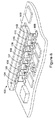
別の実施形態では、光電子エンジン104〜112を、PCBの表面に配置されたポートに直接接続するように構成することができる。図8は、本発明の実施形態にしたがう、第6の配置状態にあるバス100の組立分解等角図である。図8の例に示すように、PCB800はボート801〜809を有している。ハウジング102を、光電子エンジン104〜112の各々を露わにする開口部(孔)を含むように構成することができ、光電子エンジンを、ポート801〜809に接続するように構成することができる。その結果、バス100を逆にして、光電子エンジン104〜112の各々をポート801〜809に直接接続することができ、これによって、バス100のパッドをPCB800に接続する必要性を排除することができる。
In another embodiment, the optoelectronic engines 104-112 can be configured to connect directly to ports located on the surface of the PCB. FIG. 8 is an exploded isometric view of the
コンピュータシステムのラックやブレードサーバーの筐体内の自由空間は制限されていることが多い。データバスなどの比較的大きなコンポーネントシステムを、コンピュータシステムの込み合った内部に収容するのは難しい場合がある。本発明の実施形態は、バス100を上述のように単一のPCBに取り付けることには限定されない。PCB間に通信を提供するために、バス100を複数のPCBのエッジ(端)に結合することもできる。したがって、バス100は、バックプレーンに取って代わることができ、または、バス100は、少なくとも、バックプレーンによって提供される通信を補完することができる。PCBを、マザーボード、または、ブレードサーバー中の個々のサーバーブレードとすることができる。図9は、本発明の実施形態にしたがう、ブレードサーバーの9つのサーバーブレード901〜909に結合されたバス100を示す。図9に示すように、9つのサーバーブレード901〜909は、ブレードサーバーの筐体がない状態で示されている。各サーバーブレードはバス100のパッドに電気的に(または電子的に)結合されている。たとえば、パッド910はサーバーブレード909に結合されている。バス100は、典型的なミッドプレーンやバックプレーンよりも高いフレキシビリティを提供する。たとえば、ブレードサーバーのサーバーブレードは、動作中に振動することができ、サーバーブレードは、サーバーブレードの筐体内で均等に隔置されていなくてもよい。フレキシブルコネクタも可撓性であるため、フレキシブルコネクタは、バス100を介する通信を妨害することなく個々のサーバーブレードの振動に耐えることができ、ケーブルの可撓性(柔軟性)によって、ポートが均等に隔置されていない場合でも、パッドをそれらのポートに接続することが可能になる。
Free space in computer system racks and blade server enclosures is often limited. It can be difficult to accommodate a relatively large component system such as a data bus within a crowded interior of a computer system. Embodiments of the present invention are not limited to attaching the
本発明を特定の実施形態に関して説明したが、本発明をそれらの実施形態に限定することは意図されていない。種々の変更が当業者には明らかであろう。たとえば、バス100は、9つの光電子エンジン及び9つのフレキシブルコネクタに限定されない。光電子エンジン及びフレキシブルコネクタの数は、コンポーネントまたはサーバーブレード(バスはこれらのために機能するように構成される)の数に依存して変わりうる。他の実施形態では、フレキシブルコネクタを可撓性の光フレキシブルコネクタで置き換えることができ、この場合、電気フレキシブルコネクタ116〜124の個々のワイヤ(電線)は光ファイバーで置き換えられる。
Although the invention has been described with reference to particular embodiments, it is not intended that the invention be limited to those embodiments. Various modifications will be apparent to those skilled in the art. For example, the
以上の記述は、説明のためのものであって、本発明を完全に理解できるようにするために特定の用語を用いた。しかしながら、本発明を実施するために特定の細部は必要ではないことは当業者には明らかであろう。本発明の特定の実施形態についての上記記述は、例示及び説明のために提示されたものである。それらは、本発明を網羅することも、本発明を開示した形態そのものに限定することも意図していない。上記の教示に照らして多くの変更及び変形が可能であることは明らかである。上記実施形態は、本発明の原理及び本発明の実用的応用を最も良く説明し、これによって、当業者が、意図する特定の用途に適するように種々の変更を加えつつ本発明及び種々の実施形態を最良に利用できるようにするために図示し及び説明された。本発明の範囲は、添付の特許請求の範囲及びその等価物によって画定されることが意図されている。
The foregoing description is for purposes of explanation and specific terminology has been used in order to provide a thorough understanding of the present invention. However, it will be apparent to one skilled in the art that the specific details are not required in order to practice the invention. The foregoing descriptions of specific embodiments of the present invention have been presented for purposes of illustration and description. They are not intended to be exhaustive or to limit the invention to the precise forms disclosed. Obviously, many modifications and variations are possible in view of the above teachings. The above embodiments best illustrate the principles of the present invention and the practical application of the present invention so that those skilled in the art can make various modifications and changes to suit the particular application intended. It has been shown and described in order to make best use of the form. It is intended that the scope of the invention be defined by the appended claims and their equivalents.
Claims (14)
ハウジング(102)内に配置された複数の光電子エンジン(104〜112)と、
複数のフレキシブルコネクタ(116〜124)であって、各ケーブルが、開口部を通って前記ハウジング内に延在して、第1の端部において光電子エンジンに結合し、第2の端部において電子装置に結合する、複数のフレキシブルコネクタ
を備え、
前記フレキシブルコネクタは、空間及び接続性の要件または制限を最適化するために、前記バスを異なる配置状態をなす向きに向けることを可能にする、コンピュータバス。 A computer bus (100),
A plurality of optoelectronic engines (104-112) disposed within the housing (102);
A plurality of flexible connectors (116-124), each cable extending through the opening into the housing and coupled to the optoelectronic engine at a first end and electrons at a second end A plurality of flexible connectors for coupling to the device;
The flexible connector allows a computer bus to be oriented in different arrangements to optimize space and connectivity requirements or limitations.
光ファイバーと、
導波路と、
中空の金属導波路と、
自由空間
のうちの1つを介して前記ハウジング内に結合される、請求項1のバス。 The plurality of optoelectronic engines;
With optical fiber,
A waveguide;
A hollow metal waveguide;
The bus of claim 1, wherein the bus is coupled into the housing through one of the free spaces.
プリント回路基板(300、400、500、600、700、800)と、
サーバーブレード(901〜909)
のうちの1つを備える、請求項1のバス。 The electronic device further includes
Printed circuit boards (300, 400, 500, 600, 700, 800);
Server blade (901-909)
The bus of claim 1 comprising one of the following:
フレックス回路と、
成型加工されたリード線と、
エラストマーコネクタと、
可撓性のリボンケーブル
のうちの1つを備える、請求項1のバス。 The plurality of flexible connectors further includes
A flex circuit,
Molded lead wire,
An elastomer connector;
The bus of claim 1, comprising one of a flexible ribbon cable.
The flexible connector that allows the bus to be oriented in different arrangements further has the function of coupling the bus to a surface opposite to the surface to which the components of the electronic device are coupled. Bus.
Applications Claiming Priority (1)
| Application Number | Priority Date | Filing Date | Title |
|---|---|---|---|
| PCT/US2008/012360 WO2010050919A1 (en) | 2008-10-31 | 2008-10-31 | Variably configurable computer buses |
Publications (2)
| Publication Number | Publication Date |
|---|---|
| JP2012507781A true JP2012507781A (en) | 2012-03-29 |
| JP5199479B2 JP5199479B2 (en) | 2013-05-15 |
Family
ID=42129080
Family Applications (1)
| Application Number | Title | Priority Date | Filing Date |
|---|---|---|---|
| JP2011534461A Expired - Fee Related JP5199479B2 (en) | 2008-10-31 | 2008-10-31 | Computer bus with configurable configuration |
Country Status (6)
| Country | Link |
|---|---|
| US (1) | US8570762B2 (en) |
| EP (1) | EP2350845B1 (en) |
| JP (1) | JP5199479B2 (en) |
| KR (1) | KR101489033B1 (en) |
| CN (1) | CN102203754B (en) |
| WO (1) | WO2010050919A1 (en) |
Families Citing this family (10)
| Publication number | Priority date | Publication date | Assignee | Title |
|---|---|---|---|---|
| US9107294B2 (en) * | 2010-07-26 | 2015-08-11 | Hewlett-Packard Development Company, L.P. | System including a module |
| US8738828B2 (en) * | 2011-02-26 | 2014-05-27 | International Business Machines Corporation | System to operationally connect logic nodes |
| US8597032B2 (en) | 2011-02-26 | 2013-12-03 | International Business Machines Corporation | Electronic assemblies mating system |
| US8589608B2 (en) * | 2011-02-26 | 2013-11-19 | International Business Machines Corporation | Logic node connection system |
| US8713228B2 (en) * | 2011-02-26 | 2014-04-29 | International Business Machines Corporation | Shared system to operationally connect logic nodes |
| CN103838342A (en) * | 2012-11-23 | 2014-06-04 | 鸿富锦精密工业(深圳)有限公司 | Power source |
| US11169340B2 (en) * | 2018-03-21 | 2021-11-09 | Foxconn (Kunshan) Computer Connector Co., Ltd. | Interconnection system |
| CN109581585B (en) * | 2018-12-12 | 2021-02-23 | 苏州席正通信科技有限公司 | Three-dimensional optical waveguide backplate based on 3D prints |
| CN109655967A (en) * | 2018-12-12 | 2019-04-19 | 苏州席正通信科技有限公司 | A kind of three-dimensional optical waveguide framework based on 3D printing |
| US20220124930A1 (en) * | 2020-10-19 | 2022-04-21 | Quanta Computer Inc. | System and method for determining cable routing between electronic components within a computer chassis |
Citations (3)
| Publication number | Priority date | Publication date | Assignee | Title |
|---|---|---|---|---|
| US6685363B2 (en) * | 2000-03-28 | 2004-02-03 | Lockheed Martin Corporation | Passive self-alignment technique for array laser transmitters and receivers for fiber optic applications |
| JP2005038735A (en) * | 2003-07-16 | 2005-02-10 | Sony Corp | Device with built-in button cell |
| JP2005056618A (en) * | 2003-08-08 | 2005-03-03 | Funai Electric Co Ltd | Connection structure of flexible cable and connector |
Family Cites Families (14)
| Publication number | Priority date | Publication date | Assignee | Title |
|---|---|---|---|---|
| US5204925A (en) * | 1991-09-11 | 1993-04-20 | At&T Bell Laboratories | Optical interconnection of circuit packs |
| US5650910A (en) * | 1996-06-26 | 1997-07-22 | Sun Microsystems, Inc. | Backbone substrate for a computer |
| US6453377B1 (en) * | 1998-06-16 | 2002-09-17 | Micron Technology, Inc. | Computer including optical interconnect, memory unit, and method of assembling a computer |
| JP2001042170A (en) | 1999-07-28 | 2001-02-16 | Canon Inc | Optical wiring device, its driving method and electronic apparatus using the device |
| JP2002278922A (en) | 2001-03-16 | 2002-09-27 | Ricoh Co Ltd | Computer bus system |
| US6659656B2 (en) * | 2001-11-05 | 2003-12-09 | International Business Machines Corporation | Packaging architecture for a multiple array transceiver using a winged flexible cable for optimal wiring |
| US6876004B2 (en) * | 2001-12-04 | 2005-04-05 | Finisar Corporation | Circuit interconnect for optoelectronic device for controlled impedance at high frequencies |
| CN1236456C (en) * | 2002-12-24 | 2006-01-11 | 财团法人工业技术研究院 | Flexible photoelectric transmission bus |
| US6902329B2 (en) * | 2003-02-12 | 2005-06-07 | Lockheed Martin Corporation | Method and apparatus for the integration of parallel optical transceiver package |
| US7343059B2 (en) * | 2003-10-11 | 2008-03-11 | Hewlett-Packard Development Company, L.P. | Photonic interconnect system |
| US20050147414A1 (en) * | 2003-12-30 | 2005-07-07 | Morrow Warren R. | Low latency optical memory bus |
| US7209621B2 (en) * | 2004-07-09 | 2007-04-24 | Fujitsu Ltd. | Optical apparatuses providing optical interconnections among a plurality of electronic components |
| DE102004043254A1 (en) * | 2004-09-07 | 2006-03-30 | Siemens Ag | Connection unit for connecting an electronic device to an optical data bus |
| JP4711895B2 (en) | 2006-02-03 | 2011-06-29 | ホシデン株式会社 | Photoelectric flexible wiring board connection structure, connector and photoelectric flexible wiring board |
-
2008
- 2008-10-31 JP JP2011534461A patent/JP5199479B2/en not_active Expired - Fee Related
- 2008-10-31 WO PCT/US2008/012360 patent/WO2010050919A1/en active Application Filing
- 2008-10-31 KR KR1020117012118A patent/KR101489033B1/en active IP Right Grant
- 2008-10-31 EP EP08877841.0A patent/EP2350845B1/en active Active
- 2008-10-31 US US13/124,097 patent/US8570762B2/en active Active
- 2008-10-31 CN CN200880131815.6A patent/CN102203754B/en active Active
Patent Citations (3)
| Publication number | Priority date | Publication date | Assignee | Title |
|---|---|---|---|---|
| US6685363B2 (en) * | 2000-03-28 | 2004-02-03 | Lockheed Martin Corporation | Passive self-alignment technique for array laser transmitters and receivers for fiber optic applications |
| JP2005038735A (en) * | 2003-07-16 | 2005-02-10 | Sony Corp | Device with built-in button cell |
| JP2005056618A (en) * | 2003-08-08 | 2005-03-03 | Funai Electric Co Ltd | Connection structure of flexible cable and connector |
Also Published As
| Publication number | Publication date |
|---|---|
| KR20110091698A (en) | 2011-08-12 |
| CN102203754B (en) | 2015-08-26 |
| KR101489033B1 (en) | 2015-02-02 |
| EP2350845A4 (en) | 2014-08-13 |
| JP5199479B2 (en) | 2013-05-15 |
| US20110205718A1 (en) | 2011-08-25 |
| CN102203754A (en) | 2011-09-28 |
| EP2350845B1 (en) | 2021-12-29 |
| EP2350845A1 (en) | 2011-08-03 |
| US8570762B2 (en) | 2013-10-29 |
| WO2010050919A1 (en) | 2010-05-06 |
Similar Documents
| Publication | Publication Date | Title |
|---|---|---|
| JP5199479B2 (en) | Computer bus with configurable configuration | |
| US6805560B1 (en) | Apparatus interconnecting circuit board and mezzanine card or cards | |
| JP6208878B2 (en) | Connector system with cable bypass | |
| JP2020009433A (en) | Routing assembly | |
| US6609914B2 (en) | High speed and density circular connector for board-to-board interconnection systems | |
| US6814582B2 (en) | Rear interconnect blade for rack mounted systems | |
| US7651364B2 (en) | Circuit board assembly with light emitting element | |
| US6504725B1 (en) | Topology for PCI bus riser card system | |
| US6038048A (en) | Apparatus for communication between multiple processing modules | |
| CN111566531B (en) | Data communication system | |
| JP4771372B2 (en) | Electronic device connector, system and mounting method (PCI Express connector) | |
| US7396166B1 (en) | Optical transceiver module | |
| US20210161031A1 (en) | Fan module | |
| JP2004235636A (en) | Integrated vcsel on asic module using flexible electric connection | |
| US20110294313A1 (en) | Receptacle connector | |
| US20100158535A1 (en) | Small form-factor pluggable transceiver module | |
| TWI497847B (en) | Universal serial bus connector and method for providing universal serial bus connector with optical functionality | |
| US20230098634A1 (en) | Right-angled orthogonal connector assembly having a wire termination to a high-speed cable | |
| US7088199B2 (en) | Method and stiffener-embedded waveguide structure for implementing enhanced data transfer | |
| EP1284094B1 (en) | Electrically connecting integrated circuits and transducers | |
| CN115734472A (en) | Computing device | |
| US20200158966A1 (en) | Optical signal aggregation for optical communication in high bandwidth, high density architectures |
Legal Events
| Date | Code | Title | Description |
|---|---|---|---|
| A131 | Notification of reasons for refusal |
Free format text: JAPANESE INTERMEDIATE CODE: A131 Effective date: 20120605 |
|
| A521 | Request for written amendment filed |
Free format text: JAPANESE INTERMEDIATE CODE: A523 Effective date: 20120903 |
|
| TRDD | Decision of grant or rejection written | ||
| A01 | Written decision to grant a patent or to grant a registration (utility model) |
Free format text: JAPANESE INTERMEDIATE CODE: A01 Effective date: 20130115 |
|
| A61 | First payment of annual fees (during grant procedure) |
Free format text: JAPANESE INTERMEDIATE CODE: A61 Effective date: 20130207 |
|
| FPAY | Renewal fee payment (event date is renewal date of database) |
Free format text: PAYMENT UNTIL: 20160215 Year of fee payment: 3 |
|
| R150 | Certificate of patent or registration of utility model |
Ref document number: 5199479 Country of ref document: JP Free format text: JAPANESE INTERMEDIATE CODE: R150 Free format text: JAPANESE INTERMEDIATE CODE: R150 |
|
| R250 | Receipt of annual fees |
Free format text: JAPANESE INTERMEDIATE CODE: R250 |
|
| S111 | Request for change of ownership or part of ownership |
Free format text: JAPANESE INTERMEDIATE CODE: R313113 |
|
| R360 | Written notification for declining of transfer of rights |
Free format text: JAPANESE INTERMEDIATE CODE: R360 |
|
| R360 | Written notification for declining of transfer of rights |
Free format text: JAPANESE INTERMEDIATE CODE: R360 |
|
| R371 | Transfer withdrawn |
Free format text: JAPANESE INTERMEDIATE CODE: R371 |
|
| R250 | Receipt of annual fees |
Free format text: JAPANESE INTERMEDIATE CODE: R250 |
|
| S111 | Request for change of ownership or part of ownership |
Free format text: JAPANESE INTERMEDIATE CODE: R313113 |
|
| R350 | Written notification of registration of transfer |
Free format text: JAPANESE INTERMEDIATE CODE: R350 |
|
| R250 | Receipt of annual fees |
Free format text: JAPANESE INTERMEDIATE CODE: R250 |
|
| R250 | Receipt of annual fees |
Free format text: JAPANESE INTERMEDIATE CODE: R250 |
|
| R250 | Receipt of annual fees |
Free format text: JAPANESE INTERMEDIATE CODE: R250 |
|
| R250 | Receipt of annual fees |
Free format text: JAPANESE INTERMEDIATE CODE: R250 |
|
| R250 | Receipt of annual fees |
Free format text: JAPANESE INTERMEDIATE CODE: R250 |
|
| LAPS | Cancellation because of no payment of annual fees |