JP2012506154A - Electrostatic discharge (ESD) protection of stack IC - Google Patents
Electrostatic discharge (ESD) protection of stack IC Download PDFInfo
- Publication number
- JP2012506154A JP2012506154A JP2011532236A JP2011532236A JP2012506154A JP 2012506154 A JP2012506154 A JP 2012506154A JP 2011532236 A JP2011532236 A JP 2011532236A JP 2011532236 A JP2011532236 A JP 2011532236A JP 2012506154 A JP2012506154 A JP 2012506154A
- Authority
- JP
- Japan
- Prior art keywords
- layer
- unpatterned layer
- stage
- unpatterned
- unassembled
- Prior art date
- Legal status (The legal status is an assumption and is not a legal conclusion. Google has not performed a legal analysis and makes no representation as to the accuracy of the status listed.)
- Pending
Links
Images


Classifications
-
- H—ELECTRICITY
- H01—ELECTRIC ELEMENTS
- H01L—SEMICONDUCTOR DEVICES NOT COVERED BY CLASS H10
- H01L23/00—Details of semiconductor or other solid state devices
- H01L23/58—Structural electrical arrangements for semiconductor devices not otherwise provided for, e.g. in combination with batteries
- H01L23/60—Protection against electrostatic charges or discharges, e.g. Faraday shields
-
- H—ELECTRICITY
- H01—ELECTRIC ELEMENTS
- H01L—SEMICONDUCTOR DEVICES NOT COVERED BY CLASS H10
- H01L25/00—Assemblies consisting of a plurality of individual semiconductor or other solid state devices ; Multistep manufacturing processes thereof
- H01L25/03—Assemblies consisting of a plurality of individual semiconductor or other solid state devices ; Multistep manufacturing processes thereof all the devices being of a type provided for in the same subgroup of groups H01L27/00 - H01L33/00, or in a single subclass of H10K, H10N, e.g. assemblies of rectifier diodes
- H01L25/04—Assemblies consisting of a plurality of individual semiconductor or other solid state devices ; Multistep manufacturing processes thereof all the devices being of a type provided for in the same subgroup of groups H01L27/00 - H01L33/00, or in a single subclass of H10K, H10N, e.g. assemblies of rectifier diodes the devices not having separate containers
- H01L25/065—Assemblies consisting of a plurality of individual semiconductor or other solid state devices ; Multistep manufacturing processes thereof all the devices being of a type provided for in the same subgroup of groups H01L27/00 - H01L33/00, or in a single subclass of H10K, H10N, e.g. assemblies of rectifier diodes the devices not having separate containers the devices being of a type provided for in group H01L27/00
-
- H—ELECTRICITY
- H01—ELECTRIC ELEMENTS
- H01L—SEMICONDUCTOR DEVICES NOT COVERED BY CLASS H10
- H01L27/00—Devices consisting of a plurality of semiconductor or other solid-state components formed in or on a common substrate
- H01L27/02—Devices consisting of a plurality of semiconductor or other solid-state components formed in or on a common substrate including semiconductor components specially adapted for rectifying, oscillating, amplifying or switching and having at least one potential-jump barrier or surface barrier; including integrated passive circuit elements with at least one potential-jump barrier or surface barrier
- H01L27/04—Devices consisting of a plurality of semiconductor or other solid-state components formed in or on a common substrate including semiconductor components specially adapted for rectifying, oscillating, amplifying or switching and having at least one potential-jump barrier or surface barrier; including integrated passive circuit elements with at least one potential-jump barrier or surface barrier the substrate being a semiconductor body
-
- H—ELECTRICITY
- H01—ELECTRIC ELEMENTS
- H01L—SEMICONDUCTOR DEVICES NOT COVERED BY CLASS H10
- H01L2224/00—Indexing scheme for arrangements for connecting or disconnecting semiconductor or solid-state bodies and methods related thereto as covered by H01L24/00
- H01L2224/01—Means for bonding being attached to, or being formed on, the surface to be connected, e.g. chip-to-package, die-attach, "first-level" interconnects; Manufacturing methods related thereto
- H01L2224/26—Layer connectors, e.g. plate connectors, solder or adhesive layers; Manufacturing methods related thereto
- H01L2224/27—Manufacturing methods
- H01L2224/274—Manufacturing methods by blanket deposition of the material of the layer connector
-
- H—ELECTRICITY
- H01—ELECTRIC ELEMENTS
- H01L—SEMICONDUCTOR DEVICES NOT COVERED BY CLASS H10
- H01L25/00—Assemblies consisting of a plurality of individual semiconductor or other solid state devices ; Multistep manufacturing processes thereof
- H01L25/03—Assemblies consisting of a plurality of individual semiconductor or other solid state devices ; Multistep manufacturing processes thereof all the devices being of a type provided for in the same subgroup of groups H01L27/00 - H01L33/00, or in a single subclass of H10K, H10N, e.g. assemblies of rectifier diodes
- H01L25/04—Assemblies consisting of a plurality of individual semiconductor or other solid state devices ; Multistep manufacturing processes thereof all the devices being of a type provided for in the same subgroup of groups H01L27/00 - H01L33/00, or in a single subclass of H10K, H10N, e.g. assemblies of rectifier diodes the devices not having separate containers
- H01L25/065—Assemblies consisting of a plurality of individual semiconductor or other solid state devices ; Multistep manufacturing processes thereof all the devices being of a type provided for in the same subgroup of groups H01L27/00 - H01L33/00, or in a single subclass of H10K, H10N, e.g. assemblies of rectifier diodes the devices not having separate containers the devices being of a type provided for in group H01L27/00
- H01L25/0657—Stacked arrangements of devices
-
- H—ELECTRICITY
- H01—ELECTRIC ELEMENTS
- H01L—SEMICONDUCTOR DEVICES NOT COVERED BY CLASS H10
- H01L2924/00—Indexing scheme for arrangements or methods for connecting or disconnecting semiconductor or solid-state bodies as covered by H01L24/00
- H01L2924/01—Chemical elements
- H01L2924/01055—Cesium [Cs]
-
- H—ELECTRICITY
- H01—ELECTRIC ELEMENTS
- H01L—SEMICONDUCTOR DEVICES NOT COVERED BY CLASS H10
- H01L2924/00—Indexing scheme for arrangements or methods for connecting or disconnecting semiconductor or solid-state bodies as covered by H01L24/00
- H01L2924/10—Details of semiconductor or other solid state devices to be connected
- H01L2924/11—Device type
- H01L2924/12—Passive devices, e.g. 2 terminal devices
- H01L2924/1204—Optical Diode
- H01L2924/12044—OLED
Abstract
アセンブルされていないスタックICデバイス(60)は、アセンブルされていない段を含む。(41)アセンブルされていないスタックICデバイスは、アセンブルされていない段の上の第1のパターン形成されていない層(610)をさらに含む。第1のパターン形成されていない層は、ESDイベントからアセンブルされていない段を保護する。 The unassembled stack IC device (60) includes an unassembled stage. (41) The unassembled stacked IC device further includes a first unpatterned layer (610) on the unassembled stage. The first unpatterned layer protects the unassembled stage from ESD events.
Description
本開示は、概して、スタックされた集積回路(ICs)に関する。より詳細には、本開示は、静電放電からスタックICsを保護すること(shielding)に関する。 The present disclosure relates generally to stacked integrated circuits (ICs). More particularly, the present disclosure relates to shielding stack ICs from electrostatic discharge.
静電放電(ESD:Electrostatic discharge)イベントは、日常生活の一般的な一部であり、より大きな放電の中には、人間の感覚によって検出可能なものもある。より小さな放電は、放電が起こる表面積に対する放電強度の比率が非常に小さいため、人間の感覚によって気づかれずにいる。 Electrostatic discharge (ESD) events are a common part of everyday life, and some larger discharges can be detected by human senses. Smaller discharges are not noticed by human senses because the ratio of discharge intensity to surface area where discharge occurs is very small.
ICsは、過去数十年間にわたり、驚くほどのペースで縮小化されてきた。例として、ICsの中のトランジスタは、45nmまで縮小し、おそらく縮小し続けるであろう。トランジスタのサイズが縮小するにつれ、トランジスタ周辺の支持コンポーネントも同様に一般に縮小する。ICsの縮小は、表面積を減少させる。したがって、表面積に対する所与の放電強度の比率が、より小さいコンポーネントサイズで増加し、コンポーネントは、より広範囲のESDイベントの影響を受けやすくなる。 ICs have been shrinking at a surprising pace over the past decades. As an example, the transistors in ICs will shrink to 45 nm and will probably continue to shrink. As the size of the transistor decreases, the supporting components around the transistor generally decrease as well. The reduction of ICs reduces the surface area. Thus, the ratio of a given discharge intensity to surface area increases with a smaller component size, making the component susceptible to a wider range of ESD events.
ESDイベントは、第1の電荷の物体が、より低い第2の電荷の物体に接近または接触すると、起こる。その差が、単一のイベントとして放電される。2つの物体がほぼ等しい電荷となるように、第1の物体から第2の物体への急激な電荷の移動が起こる。より低い電荷の物体がICである場合、放電は、ICを通る最小抵抗経路を見つけようと試みる。典型的に、この経路は、相互接続を通って流れる。放電に関連づけられたエネルギーに耐えることのできない、この経路の任意の一部は、損傷を受ける。そのような損傷は、しばしばゲート酸化物において起こり、それは、概して、ICsにおいて放電の影響を最も受けやすいリンクである。ゲート酸化物は、損傷すると、典型的には絶縁体から導電体に変わるので、ICは、もはや所望されるように機能しない。ESDイベントによる別の損傷メカニズムは、デバイスにおけるショートを生み出すスルーシリコンビア(through silicon via)でのゲート酸化物の破断、または、デバイスにおける開路を生み出す相互接続での金属溶融を含む。 An ESD event occurs when a first charged object approaches or contacts a lower second charged object. The difference is discharged as a single event. An abrupt charge transfer from the first object to the second object occurs so that the two objects have approximately equal charges. If the lower charge object is an IC, the discharge will attempt to find the minimum resistance path through the IC. This path typically flows through the interconnect. Any part of this path that cannot withstand the energy associated with the discharge is damaged. Such damage often occurs in the gate oxide, which is generally the most susceptible link to discharge in ICs. Since the gate oxide typically changes from an insulator to a conductor when damaged, the IC no longer functions as desired. Another damage mechanism due to an ESD event includes rupture of the gate oxide at a through silicon via that creates a short in the device, or metal melting at the interconnect that creates an open circuit in the device.
集積回路の製造が行われる製造現場は、製造中の集積回路でのESDを防止する手順を、十分に発達させ、実行してきた。たとえば、設計上の規則が、大きな電荷が製造中に蓄積しないことを保証するために、使用されている。慣例的に、ESD保護構造は、基板にも組み入れられ、保護するデバイスに接続されている。これらの構造は、もしそうでなければ能動回路のために使用されるであろう、基板上のかなり多くの面積(各ESDバッファにつき数十乃至数百平方ミクロン)を消費する。しかしながら、ESDイベントは、ICの製造プロセス中にも起こりうる。ICにおけるそのような損傷箇所を検出することは困難であり、そのような損傷が製造中に起こったという第1の徴候が現れるのは、典型的に、最終製品が望むように機能しないときである。結果として、膨大な量の時間と資源が、正常に機能しないデバイスの製造に費やされうる。 Manufacturing sites where integrated circuit manufacturing takes place have fully developed and implemented procedures to prevent ESD in integrated circuits being manufactured. For example, design rules are used to ensure that large charges do not accumulate during manufacturing. Conventionally, the ESD protection structure is also incorporated into the substrate and connected to the protecting device. These structures consume a considerable amount of area on the substrate (tens to hundreds of square microns for each ESD buffer) that would otherwise be used for active circuits. However, ESD events can also occur during the IC manufacturing process. It is difficult to detect such a damage spot in an IC, and the first indication that such damage has occurred during manufacturing is typically when the final product does not function as desired. is there. As a result, a tremendous amount of time and resources can be spent on manufacturing devices that do not function properly.
ICsの性能をさらに進歩させる1つの最近の発展は、集積回路をスタックして3−D構造またはスタックICを形成するようにしたことである。これは、複数のコンポーネントを、別の段の単一のチップに組み入れられるようにさせる。たとえば、メモリキャッシュは、マイクロプロセッサの一番上に組み入れられうる。結果として生じるスタックICは、著しくより高密度のデバイス、および、著しくより複雑な製造方法を有する。スタックICsにおける段から段への接続(tier−to−tier connection)の密度が、100,000/cm2を超えることが見込まれる。 One recent development that further advances the performance of ICs is the stacking of integrated circuits to form 3-D structures or stacked ICs. This allows multiple components to be incorporated into a single chip at another stage. For example, the memory cache can be built on top of the microprocessor. The resulting stack IC has significantly higher density devices and significantly more complex manufacturing methods. Density connection to stage from stage in the stack ICs (tier-to-tier connection ) is expected to be greater than 100,000 / cm 2.
スタックICsでは、製造者が、1つの製造現場で、第1のIC製造プロセスのセットを行い、第2の段についての第2の製造プロセスのセットを行う第2の製造現場へ、そのICの段を出荷する場合がある。そして、第3の現場が、スタックICに段をアセンブルする場合がある。集積回路の段が、製造現場の制御された環境を離れると、それらは、スタックIC全体を無用なものにしうる可能性のあるESDイベントにさらされる。個々の段がスタック(すなわち、スタックICを作るために、ともに結合)される前、段は、ESDイベントに対し特に弱い。 In stack ICs, a manufacturer performs a first IC manufacturing process set at one manufacturing site and a second manufacturing site for a second set of manufacturing processes for the second stage. There is a case where a stage is shipped. The third site may then assemble the steps into the stack IC. As integrated circuit stages leave the controlled environment of the manufacturing floor, they are exposed to ESD events that can potentially render the entire stack IC useless. Before individual stages are stacked (ie, combined together to make a stack IC), the stages are particularly vulnerable to ESD events.
したがって、製造プロセス中に制御された環境の外へ移送される際、スタックされた集積回路の個々の段をESDイベントから保護する必要がある。 Therefore, there is a need to protect individual stages of stacked integrated circuits from ESD events when transported out of a controlled environment during the manufacturing process.
開示の一態様によると、アセンブルされていないスタックICデバイスは、アセンブルされていない段(unassembled tier)を含む。アセンブルされていないスタックICデバイスは、アセンブルされていない段の上に、第1のパターン形成されていない層をさらに含む。第1のパターン形成されていない層は、ESDイベントからアセンブルされていない段を保護する。 According to one aspect of the disclosure, an unassembled stacked IC device includes an unassembled tier. The unassembled stacked IC device further includes a first unpatterned layer on the unassembled stage. The first unpatterned layer protects the unassembled stage from ESD events.
開示の別の態様によると、スタックICデバイスを製造するための方法は、スタックICデバイスの段を製造することを含む。この方法は、組み立て工場へ移送する前に、その段の上にパターン形成されていない層を堆積させることを、さらに含む。パターン形成されていない層は、ESDイベントから段を保護する。 According to another aspect of the disclosure, a method for manufacturing a stacked IC device includes manufacturing a stage of the stacked IC device. The method further includes depositing an unpatterned layer on the step prior to transfer to the assembly plant. The unpatterned layer protects the step from ESD events.
開示のさらに別の態様によると、スタックICデバイスを製造するための方法は、スタックICデバイスの段をスタックICデバイスに組み込まれるようにさせるために、ESDイベントからスタックICデバイスの段を保護する、パターン形成されていない層を変えることを含む。この方法は、スタックICデバイスに段を組み込むことをさらに含む。 According to yet another aspect of the disclosure, a method for manufacturing a stack IC device protects a stage of a stack IC device from an ESD event to cause the stage of the stack IC device to be incorporated into the stack IC device. Including changing the unpatterned layer. The method further includes incorporating a stage into the stacked IC device.
開示のさらなる態様によると、アセンブルされていないスタックICデバイスは、スタックICデバイスをアセンブルする前に、ESDイベントからアセンブルされていないスタックICデバイスを保護するための手段を含む。 According to a further aspect of the disclosure, the unassembled stack IC device includes means for protecting the unassembled stack IC device from an ESD event prior to assembling the stack IC device.
前述したものは、以下の詳細な説明がよりよく理解されうるように、本開示の特徴および技術的利点をいくぶん広く述べている。開示される特許請求の主題を形成する追加の特徴および利点が、以下に説明される。開示される概念および特定の実施形態が、本開示と同一の目的を遂行するための他の構造を変更または設計するための基礎として、容易に利用されうることが、当業者によって理解されるべきである。そのような等価の構造が、添付の特許請求の範囲に記載された開示の技術から逸脱しないということも、当業者によって認識されるべきである。さらなる目的および利点とともに、その構成および動作方法の両方について、開示の特徴であると確信される新規な特徴は、添付の図面と関連して考慮されると、以下の説明からよりよく理解されるであろう。しかしながら、図面の各々は、例示および説明のみの目的で提供され、本開示の限定の定義として意図されるものではないということが、明確に理解される。 The foregoing has outlined rather broadly the features and technical advantages of the present disclosure in order that the detailed description that follows may be better understood. Additional features and advantages that form the disclosed claimed subject matter are described below. It should be understood by those skilled in the art that the disclosed concepts and specific embodiments can be readily utilized as a basis for modifying or designing other structures for carrying out the same purposes as the present disclosure. It is. It should also be recognized by those skilled in the art that such equivalent constructions do not depart from the disclosed technology recited in the appended claims. The novel features believed to be disclosed features, both with respect to their construction and method of operation, along with further objects and advantages, will be better understood from the following description when considered in conjunction with the accompanying drawings. Will. However, it is clearly understood that each of the drawings is provided for purposes of illustration and description only and is not intended as a definition of the limitations of the present disclosure.
本開示のより完全な理解のために、添付の図面とあわせて理解される以下の詳細な説明が、ここで参照される。 For a more complete understanding of the present disclosure, reference is now made to the following detailed description, taken in conjunction with the accompanying drawings, in which:
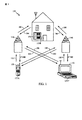
図1は、開示の実施形態が有利に用いられうる例示的な無線通信システム100を示すブロック図である。例示のために、図1は、3つの遠隔ユニット120,130,および150と、2つの基地局140を示している。典型的な無線通信システムは、さらに多くの遠隔ユニットおよび基地局を有しうるということが認識されるであろう。遠隔ユニット120,130,および150は、ICデバイス125A,125B,および125Cを含み、それらは、ここに開示される回路を含む。ICを含む任意のデバイスは、基地局、スイッチングデバイス、およびネットワーク機器を含み、ここに開示される回路をさらに含みうるということが認識されるであろう。図1は、基地局140から遠隔ユニット120,130,および150へのフォワードリンク信号180と、遠隔ユニット120,130,および150から基地局140へのリバースリンク信号190とを示す。
FIG. 1 is a block diagram illustrating an example
図1において、遠隔ユニット120は、移動電話として示され、遠隔ユニット130は、携帯用コンピュータとして示され、遠隔ユニット150は、無線ローカルループシステムにおける固定位置の遠隔ユニットとして示されている。たとえば、遠隔ユニットは、セル式電話、ハンドヘルド型のパーソナル通信システム(PCS)ユニット、携帯情報端末のような携帯データユニット、またはメーター示度機器のような固定位置のデータユニットであることができる。図1は、開示された教示による遠隔ユニットを示しているが、開示は、これらの例示的に示されたユニットに限定されるものではない。開示は、以下に説明するようなESD保護機構(ESD protection scheme)を含む任意のデバイスにおいて好適に用いられることができる。
In FIG. 1,
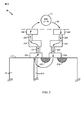
ここで図2を参照し、ICsにおける1つのESDの課題が説明される。図2は、回路ダイ、および回路を通るESD経路を示すブロック図である。デバイス20は、能動面210を有する基板21を含む。能動面210には、電界効果トランジスタ(FETs:field effect transistor)のPNP接合を作るのに使用されるドープ処理された領域212がある。能動面210の表面に構築されているのは、特定の集積回路の生産用の設計によって特定される多数の層である。たとえば、接触層220は、中間層224に結合されうる相互接続222に結合されうる。中間層224は、段から段への接続228に結合されうる相互接続226に結合されうる。さらに、スルーシリコンビア(TSV:through silicon via)214が示されているが、これは、接触層220に結合されうる。
With reference now to FIG. 2, one ESD issue in ICs is described. FIG. 2 is a block diagram illustrating a circuit die and an ESD path through the circuit.
ウェーハの取り扱いおよび処理中に、デバイス20よりも相対的に高い電荷のESDソース23が、基板21に接近または接触する場合がある。たとえば、ESDソース23が、段から段への接続228のような露出した接続と接触する場合がある。露出した接続との接近または接触により、ESDソース23は、平衡状態に達するようにデバイス20に放電する。電流フロー24が、完全な回路を作るように形成される。電流フロー24は、デバイス20を通る最小抵抗経路に沿う。この例において、この経路は、段から段への接続228、相互接続226、中間層224、相互接続222、および接触層220を通りうる。そして、電流フロー24は、基板21を通ってスルーシリコンビア214へ、さらに、接触層220、相互接続222、中間層224、相互接続226、および段から段への接続228を通って流れ、ESDソース23との閉路を作る。電流フロー24の経路にあるものは何でも、先に説明されたメカニズムによって、デバイス20の故障を生じうる損傷を被る可能性がありうる。
During wafer handling and processing, an
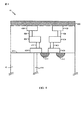
ここで図3を参照し、ESDイベントによる損傷を防止するための従来の手段が考察される。説明のために、デバイス30は、デバイス20と同様の回路構成を有する。静電放電による損傷の防止は、接続312によって能動回路に接続されたESDデバイス310によって達成される。ESDデバイスは、たとえば、順方向バイアス保護(forward bias protection)のためのダイオード、および、逆バイアス保護(reverse bias protection)のための追加のダイオードでありうる。静電放電イベントが起こり、デバイス30を通って電流が送られると、ESDデバイスは、感度のよいコンポーネントからESDデバイス310に向けて電流を分流する最小抵抗経路を作り出す。デバイス30において、ESDイベントによる損傷は減少するが、さもなければ能動回路のために使用されるであろう面積を消費するという犠牲を払うことになる。さらに、ESDデバイス310は、デバイスの動作中、漏出電流によってパワーを消費する。バッテリーのパワーによって動作する通信デバイスにおいて、このパワー消費は、デバイスの動作を短くする。さらに、ESDデバイス310は、デバイス30のコンポーネントの寄生的な負荷(parasitic load)となる。
Referring now to FIG. 3, conventional means for preventing damage due to ESD events will be discussed. For the sake of explanation, the
本開示の態様によると、デバイスとそのコンポーネントは、デバイスに薄膜コーティングを堆積(deposit)させることによって、制御された環境外であっても、製造プロセス中にESD損傷から保護される。このコーティングは、絶縁体(ケイ素酸化物、窒化ケイ素、またはポリマー、等)、半導体(ケイ素、等)、または金属(銅、等)であることができる。金属または半導体のコーティングは、ESDイベントによって生じる電流フローのために相対的に低抵抗の経路を供給することによって、電流が保護層の下の感度のよいコンポーネントに損傷を与えることを防止する。あるいは、絶縁体コーティングが、ESDイベントによる電流フローが保護層の下のコンポーネントを通ることを防止する。コーティングのいくつかの実施形態がさらに詳細に説明される。 In accordance with aspects of the present disclosure, the device and its components are protected from ESD damage during the manufacturing process, even outside the controlled environment, by depositing a thin film coating on the device. The coating can be an insulator (silicon oxide, silicon nitride, or polymer, etc.), a semiconductor (silicon, etc.), or a metal (copper, etc.). The metal or semiconductor coating prevents the current from damaging sensitive components under the protective layer by providing a relatively low resistance path for the current flow caused by the ESD event. Alternatively, the insulator coating prevents current flow due to the ESD event from passing through the component under the protective layer. Several embodiments of the coating are described in further detail.
1つの実施形態によると、絶縁保護層が、ESDイベントからデバイスを保護するために使用される。絶縁保護層に使用されうるいくつかの材料は、ケイ素酸化物、窒化ケイ素、ポリマー、フォトレジスト、またはスピンオンガラス(SOGs:spin on glasses)を含む。保護層の厚さは、回路設計および製造プロセスに基づいて異なりうる。1つの実施形態によると、層の厚さは、100乃至50000オングストロームである。追加のESD防止が所望される場合、厚さは増加しうる。より厚い絶縁層は、破損を経験し、かつ、ESDソースからデバイスへの電流フローを許すまでに、より大きな電位差に耐えることができる。ESD防止が十分であり、より迅速な製造プロセスが所望される場合、層はより薄くてもよい。より薄い絶縁層は、将来の処理において、より容易かつ迅速に除去またはパターン形成される。1つの実施形態において、層は、移送に機械的に耐えるのに十分な厚さである。 According to one embodiment, an insulating protective layer is used to protect the device from ESD events. Some materials that can be used for the insulating protective layer include silicon oxide, silicon nitride, polymers, photoresists, or spin on glasses (SOGs). The thickness of the protective layer can vary based on circuit design and manufacturing processes. According to one embodiment, the layer thickness is between 100 and 50000 angstroms. If additional ESD protection is desired, the thickness can be increased. A thicker insulating layer can withstand a greater potential difference before experiencing failure and allowing current flow from the ESD source to the device. If ESD prevention is sufficient and a faster manufacturing process is desired, the layer may be thinner. Thinner insulating layers are more easily and quickly removed or patterned in future processing. In one embodiment, the layer is thick enough to mechanically withstand transport.
ここで図4を参照し、絶縁保護層の保護性能が説明される。図4は、絶縁保護層を使用してESDイベントによる損傷を防止するための例示的な配列を示すブロック図である。説明のために、デバイス40は、デバイス20と同様の構成を有する。段から段への接続428の製造が完了した後、酸化物の層430が、デバイス40に堆積させられる。酸化物の層430は、パターン形成されておらず、連続する材料層のままである。
Here, with reference to FIG. 4, the protection performance of an insulating protective layer is demonstrated. FIG. 4 is a block diagram illustrating an exemplary arrangement for using an insulating protective layer to prevent damage from an ESD event. For the sake of explanation, the
絶縁保護層が堆積させられ、デバイスが第2の制御された環境(たとえば、検査および組み立て工場)に移送された後、絶縁保護層は、スタックICのアセンブリの前に除去されうる。1つの実施形態によると、層は、ウェットまたはドライエッチングといった利用可能な方法を使用して取り除かれうる(stripped)。別の実施形態によると、保護層は、接触(contact)が、絶縁保護層の下の段から段への接続に対して行われうるように、パターン形成されることもできる。絶縁保護層における開口部は、エッチングされ、下の段から段への接続を出現させる。そして、金属接触が、エッチングされた開口部に堆積させられることができる。これらのエッチングされた開口部が、ここでさらに詳細に説明される。 After the insulating protective layer is deposited and the device is transferred to a second controlled environment (eg, inspection and assembly plant), the insulating protective layer can be removed prior to stack IC assembly. According to one embodiment, the layer can be stripped using available methods such as wet or dry etching. According to another embodiment, the protective layer can also be patterned such that contact can be made to the step-to-step connection below the insulating protective layer. The opening in the insulating protective layer is etched to reveal a connection from bottom to stage. Metal contacts can then be deposited in the etched openings. These etched openings are now described in further detail.
図5は、エッチング処理後の絶縁保護層を使用してESDイベントによる損傷を防止するための例示的な配列を示すブロック図である。説明のために、デバイス50は、デバイス40と同様の構成を有する。開口部510は、酸化物の層430にエッチングされる。段から段への接続428への接触は、追加の段を段50の上にスタックされるようにさせる開口部510を通して行われうる。
FIG. 5 is a block diagram illustrating an exemplary arrangement for preventing damage due to an ESD event using an insulating protective layer after etching. For the sake of explanation, the
別の実施形態によると、金属の保護層または半導体の保護層が、制御された環境外で、ESDイベントからデバイスを保護しうる。そのような配列において、最終接続層は、パターン形成されないままであり、パターン形成されていない金属層がデバイスの表面上に残る結果となる。層は、パターン形成されないままなので、ESDイベントにより生じる任意の電流は、ICを通らずに保護層を通って進む。最終接続は、第2の製造現場に移送された後に、保護金属層からパターン形成される。金属は、デバイスの設計によって、たとえば、銅またはアルミニウムであることができる。1つの実施形態では、ポリシリコン等の半導体材料が使用される。保護層の厚さは、移送に機械的に耐え、かつ、ESDソースから見込まれる電流密度に電気的に耐えるのに十分な厚さであるべきである。 According to another embodiment, a metal protection layer or a semiconductor protection layer may protect the device from ESD events outside of a controlled environment. In such an arrangement, the final connection layer remains unpatterned, resulting in an unpatterned metal layer remaining on the surface of the device. Since the layer remains unpatterned, any current caused by the ESD event travels through the protective layer, not through the IC. The final connection is patterned from the protective metal layer after being transferred to the second manufacturing site. The metal can be, for example, copper or aluminum, depending on the device design. In one embodiment, a semiconductor material such as polysilicon is used. The thickness of the protective layer should be sufficient to mechanically withstand transport and electrically withstand the current density expected from the ESD source.
ここで図6を参照し、導電保護層の保護性能が説明される。図6は、導電保護層を使用してESDイベントによる損傷を防止するための例示的な配列を示すブロック図である。説明のために、デバイス60は、デバイス20と同様の構成を有する。この例では、段から段への接続428は、製造されていない。その代わりに、保護金属層610が、デバイス60の表面上に残っている。デバイス60がESDソース62に接触すると、電流フロー63が、形成され、電流をESDソース62からデバイス60へ流れるようにさせる。保護金属層610が、最小抵抗経路であり、電流フロー63は、保護金属層610全体を通る。このようにして、保護金属層610の下のコンポーネントへの損傷は減少する。
Here, the protection performance of the conductive protective layer will be described with reference to FIG. FIG. 6 is a block diagram illustrating an exemplary arrangement for using a conductive protective layer to prevent damage from an ESD event. For illustration purposes, the
金属保護層の場合、付加的なコストまたは手順が、製造プロセスに追加されることはない。典型的にはパターン形成されて相互接続を形成する金属層が、パターン形成されないままなので、連続する金属層が、ダイの表面上に残る。この金属層は、ダイが別の製造施設に到達し、その際に層が相互接続にパターン形成されるまで、保護層としての役割を果たす。絶縁保護層の場合、付加的な手順および層が遂行される。しかしながら、これらの層の付加的なコストは、ケイ素でESDデバイスを製造しないことから得られる節約、およびケイ素の占有面積における節約によって、相殺される。 In the case of a metal protective layer, no additional costs or procedures are added to the manufacturing process. Since the metal layer that is typically patterned to form the interconnect remains unpatterned, a continuous metal layer remains on the surface of the die. This metal layer serves as a protective layer until the die reaches another manufacturing facility, whereupon the layer is patterned into interconnects. In the case of an insulating protective layer, additional procedures and layers are performed. However, the additional cost of these layers is offset by the savings from not manufacturing ESD devices with silicon, and the savings in silicon footprint.
特定の回路が説明されたが、開示された回路のすべてが、開示を実現するために必要とされるわけではないということが当業者に理解されうる。さらに、開示に焦点を当て続けるために、特定の周知の回路は説明されていない。 Although specific circuits have been described, it can be understood by one of ordinary skill in the art that not all of the disclosed circuits are required to implement the disclosure. Moreover, certain well-known circuits have not been described in order to continue focusing on the disclosure.
本開示およびその利点が詳細に説明されたが、さまざまな変更、代用、および代替が、添付の特許請求の範囲によって定義された開示技術から逸脱することなく、ここに行われることが可能であるということが理解されるべきである。さらに、本願の範囲は、明細書で説明された、プロセス、機械、製造、物の組成、手段、方法、およびステップの特定の実施形態に限定されることを意図しない。当業者が本開示から容易に理解するように、ここで説明された対応する実施形態と、実質的に同一の機能を実行する、または、実質的に同一の結果を達成する、現在すでに存在する、または後に開発される、プロセス、機械、製造、物の組成、手段、方法、またはステップが、本開示によって利用されうる。このように、添付の特許請求の範囲は、そのようなプロセス、機械、製造、物の組成、手段、方法、またはステップを、その範囲内に含むことが意図される。 Although the present disclosure and its advantages have been described in detail, various changes, substitutions, and alternatives can be made here without departing from the disclosed technology as defined by the appended claims. It should be understood. Furthermore, the scope of the present application is not intended to be limited to the specific embodiments of the processes, machines, manufacture, product compositions, means, methods, and steps described in the specification. As one of ordinary skill in the art will readily appreciate from the present disclosure, there is currently an existing embodiment that performs substantially the same function or achieves substantially the same results as the corresponding embodiments described herein. Any process, machine, manufacture, product composition, means, method, or step developed later, may be utilized by the present disclosure. Thus, the appended claims are intended to include within their scope such processes, machines, manufacture, compositions of matter, means, methods, or steps.
Claims (25)
前記アセンブルされていない段の上の第1のパターン形成されていない層であって、ESDイベントから前記アセンブルされていない段を保護する、前記第1のパターン形成されていない層と
を含む、アセンブルされていないスタックICデバイス。 Unassembled steps,
An assembly comprising: a first unpatterned layer above the unassembled step, the first unpatterned layer protecting the unassembled step from an ESD event. Stack IC device that is not done.
組立工場に移送する前に前記段の上にパターン形成されていない層を堆積させることであって、前記パターン形成されていない層は、ESDイベントから前記段を保護する、ことと
を含む、スタックICデバイスを製造するための方法。 Manufacturing the stage of the stacked IC device;
Stacking an unpatterned layer on the step prior to transfer to an assembly plant, wherein the unpatterned layer protects the step from an ESD event. A method for manufacturing an IC device.
前記スタックICデバイスに、前記段を組み込むことと
を含む、スタックICデバイスを製造するための方法。 Changing an unpatterned layer that protects the stage of the stack IC device from an ESD event to allow the stage of the stack IC device to be incorporated into the stack IC device;
Incorporating the stage into the stacked IC device.
Applications Claiming Priority (3)
| Application Number | Priority Date | Filing Date | Title |
|---|---|---|---|
| US12/251,802 US20100091475A1 (en) | 2008-10-15 | 2008-10-15 | Electrostatic Discharge (ESD) Shielding For Stacked ICs |
| US12/251,802 | 2008-10-15 | ||
| PCT/US2009/060764 WO2010045413A1 (en) | 2008-10-15 | 2009-10-15 | Electrostatic discharge (esd) shielding for stacked ics |
Related Child Applications (1)
| Application Number | Title | Priority Date | Filing Date |
|---|---|---|---|
| JP2014192539A Division JP5917639B2 (en) | 2008-10-15 | 2014-09-22 | Electrostatic discharge (ESD) protection of stack IC |
Publications (1)
| Publication Number | Publication Date |
|---|---|
| JP2012506154A true JP2012506154A (en) | 2012-03-08 |
Family
ID=41484024
Family Applications (2)
| Application Number | Title | Priority Date | Filing Date |
|---|---|---|---|
| JP2011532236A Pending JP2012506154A (en) | 2008-10-15 | 2009-10-15 | Electrostatic discharge (ESD) protection of stack IC |
| JP2014192539A Expired - Fee Related JP5917639B2 (en) | 2008-10-15 | 2014-09-22 | Electrostatic discharge (ESD) protection of stack IC |
Family Applications After (1)
| Application Number | Title | Priority Date | Filing Date |
|---|---|---|---|
| JP2014192539A Expired - Fee Related JP5917639B2 (en) | 2008-10-15 | 2014-09-22 | Electrostatic discharge (ESD) protection of stack IC |
Country Status (7)
| Country | Link |
|---|---|
| US (1) | US20100091475A1 (en) |
| EP (1) | EP2347441A1 (en) |
| JP (2) | JP2012506154A (en) |
| KR (1) | KR101266079B1 (en) |
| CN (1) | CN102171824A (en) |
| TW (1) | TW201030934A (en) |
| WO (1) | WO2010045413A1 (en) |
Families Citing this family (75)
| Publication number | Priority date | Publication date | Assignee | Title |
|---|---|---|---|---|
| US8873585B2 (en) | 2006-12-19 | 2014-10-28 | Corning Optical Communications Wireless Ltd | Distributed antenna system for MIMO technologies |
| WO2008103375A2 (en) | 2007-02-19 | 2008-08-28 | Mobileaccess Networks Ltd. | Method and system for improving uplink performance |
| US20100054746A1 (en) | 2007-07-24 | 2010-03-04 | Eric Raymond Logan | Multi-port accumulator for radio-over-fiber (RoF) wireless picocellular systems |
| US8175459B2 (en) | 2007-10-12 | 2012-05-08 | Corning Cable Systems Llc | Hybrid wireless/wired RoF transponder and hybrid RoF communication system using same |
| WO2009053910A2 (en) | 2007-10-22 | 2009-04-30 | Mobileaccess Networks Ltd. | Communication system using low bandwidth wires |
| US8175649B2 (en) | 2008-06-20 | 2012-05-08 | Corning Mobileaccess Ltd | Method and system for real time control of an active antenna over a distributed antenna system |
| WO2009081376A2 (en) * | 2007-12-20 | 2009-07-02 | Mobileaccess Networks Ltd. | Extending outdoor location based services and applications into enclosed areas |
| WO2010090999A1 (en) | 2009-02-03 | 2010-08-12 | Corning Cable Systems Llc | Optical fiber-based distributed antenna systems, components, and related methods for monitoring and configuring thereof |
| EP2394379B1 (en) | 2009-02-03 | 2016-12-28 | Corning Optical Communications LLC | Optical fiber-based distributed antenna systems, components, and related methods for calibration thereof |
| US9673904B2 (en) | 2009-02-03 | 2017-06-06 | Corning Optical Communications LLC | Optical fiber-based distributed antenna systems, components, and related methods for calibration thereof |
| CN102232191B (en) | 2009-02-08 | 2015-07-08 | 康宁移动接入有限公司 | Communication system using cables carrying Ethernet signals |
| US9590733B2 (en) | 2009-07-24 | 2017-03-07 | Corning Optical Communications LLC | Location tracking using fiber optic array cables and related systems and methods |
| US8548330B2 (en) | 2009-07-31 | 2013-10-01 | Corning Cable Systems Llc | Sectorization in distributed antenna systems, and related components and methods |
| US8280259B2 (en) | 2009-11-13 | 2012-10-02 | Corning Cable Systems Llc | Radio-over-fiber (RoF) system for protocol-independent wired and/or wireless communication |
| US8275265B2 (en) | 2010-02-15 | 2012-09-25 | Corning Cable Systems Llc | Dynamic cell bonding (DCB) for radio-over-fiber (RoF)-based networks and communication systems and related methods |
| AU2011232897B2 (en) | 2010-03-31 | 2015-11-05 | Corning Optical Communications LLC | Localization services in optical fiber-based distributed communications components and systems, and related methods |
| US20110268446A1 (en) | 2010-05-02 | 2011-11-03 | Cune William P | Providing digital data services in optical fiber-based distributed radio frequency (rf) communications systems, and related components and methods |
| US9525488B2 (en) | 2010-05-02 | 2016-12-20 | Corning Optical Communications LLC | Digital data services and/or power distribution in optical fiber-based distributed communications systems providing digital data and radio frequency (RF) communications services, and related components and methods |
| US8570914B2 (en) | 2010-08-09 | 2013-10-29 | Corning Cable Systems Llc | Apparatuses, systems, and methods for determining location of a mobile device(s) in a distributed antenna system(s) |
| CN103119865A (en) | 2010-08-16 | 2013-05-22 | 康宁光缆系统有限责任公司 | Remote antenna clusters and related systems, components, and methods supporting digital data signal propagation between remote antenna units |
| US9160449B2 (en) | 2010-10-13 | 2015-10-13 | Ccs Technology, Inc. | Local power management for remote antenna units in distributed antenna systems |
| US9252874B2 (en) | 2010-10-13 | 2016-02-02 | Ccs Technology, Inc | Power management for remote antenna units in distributed antenna systems |
| EP2643947B1 (en) | 2010-11-24 | 2018-09-19 | Corning Optical Communications LLC | Power distribution module(s) capable of hot connection and/or disconnection for distributed antenna systems, and related power units, components, and methods |
| US11296504B2 (en) | 2010-11-24 | 2022-04-05 | Corning Optical Communications LLC | Power distribution module(s) capable of hot connection and/or disconnection for wireless communication systems, and related power units, components, and methods |
| TWI416706B (en) * | 2010-12-20 | 2013-11-21 | Univ Nat Chiao Tung | Esd structure for 3d ic |
| WO2012115843A1 (en) | 2011-02-21 | 2012-08-30 | Corning Cable Systems Llc | Providing digital data services as electrical signals and radio-frequency (rf) communications over optical fiber in distributed communications systems, and related components and methods |
| US8633562B2 (en) * | 2011-04-01 | 2014-01-21 | Qualcomm Incorporated | Voltage switchable dielectric for die-level electrostatic discharge (ESD) protection |
| CN103609146B (en) | 2011-04-29 | 2017-05-31 | 康宁光缆系统有限责任公司 | For increasing the radio frequency in distributing antenna system(RF)The system of power, method and apparatus |
| EP2702710A4 (en) | 2011-04-29 | 2014-10-29 | Corning Cable Sys Llc | Determining propagation delay of communications in distributed antenna systems, and related components, systems and methods |
| WO2013142662A2 (en) | 2012-03-23 | 2013-09-26 | Corning Mobile Access Ltd. | Radio-frequency integrated circuit (rfic) chip(s) for providing distributed antenna system functionalities, and related components, systems, and methods |
| EP2832012A1 (en) | 2012-03-30 | 2015-02-04 | Corning Optical Communications LLC | Reducing location-dependent interference in distributed antenna systems operating in multiple-input, multiple-output (mimo) configuration, and related components, systems, and methods |
| US9781553B2 (en) | 2012-04-24 | 2017-10-03 | Corning Optical Communications LLC | Location based services in a distributed communication system, and related components and methods |
| EP2842245A1 (en) | 2012-04-25 | 2015-03-04 | Corning Optical Communications LLC | Distributed antenna system architectures |
| WO2013181247A1 (en) | 2012-05-29 | 2013-12-05 | Corning Cable Systems Llc | Ultrasound-based localization of client devices with inertial navigation supplement in distributed communication systems and related devices and methods |
| US9154222B2 (en) | 2012-07-31 | 2015-10-06 | Corning Optical Communications LLC | Cooling system control in distributed antenna systems |
| WO2014024192A1 (en) | 2012-08-07 | 2014-02-13 | Corning Mobile Access Ltd. | Distribution of time-division multiplexed (tdm) management services in a distributed antenna system, and related components, systems, and methods |
| US9455784B2 (en) | 2012-10-31 | 2016-09-27 | Corning Optical Communications Wireless Ltd | Deployable wireless infrastructures and methods of deploying wireless infrastructures |
| US10257056B2 (en) | 2012-11-28 | 2019-04-09 | Corning Optical Communications LLC | Power management for distributed communication systems, and related components, systems, and methods |
| CN105308876B (en) | 2012-11-29 | 2018-06-22 | 康宁光电通信有限责任公司 | Remote unit antennas in distributing antenna system combines |
| US9647758B2 (en) | 2012-11-30 | 2017-05-09 | Corning Optical Communications Wireless Ltd | Cabling connectivity monitoring and verification |
| US9158864B2 (en) | 2012-12-21 | 2015-10-13 | Corning Optical Communications Wireless Ltd | Systems, methods, and devices for documenting a location of installed equipment |
| US9497706B2 (en) | 2013-02-20 | 2016-11-15 | Corning Optical Communications Wireless Ltd | Power management in distributed antenna systems (DASs), and related components, systems, and methods |
| WO2014199384A1 (en) | 2013-06-12 | 2014-12-18 | Corning Optical Communications Wireless, Ltd. | Voltage controlled optical directional coupler |
| EP3008828B1 (en) | 2013-06-12 | 2017-08-09 | Corning Optical Communications Wireless Ltd. | Time-division duplexing (tdd) in distributed communications systems, including distributed antenna systems (dass) |
| US9247543B2 (en) | 2013-07-23 | 2016-01-26 | Corning Optical Communications Wireless Ltd | Monitoring non-supported wireless spectrum within coverage areas of distributed antenna systems (DASs) |
| US9661781B2 (en) | 2013-07-31 | 2017-05-23 | Corning Optical Communications Wireless Ltd | Remote units for distributed communication systems and related installation methods and apparatuses |
| WO2015029028A1 (en) | 2013-08-28 | 2015-03-05 | Corning Optical Communications Wireless Ltd. | Power management for distributed communication systems, and related components, systems, and methods |
| US9385810B2 (en) | 2013-09-30 | 2016-07-05 | Corning Optical Communications Wireless Ltd | Connection mapping in distributed communication systems |
| EP3064032A1 (en) | 2013-10-28 | 2016-09-07 | Corning Optical Communications Wireless Ltd | Unified optical fiber-based distributed antenna systems (dass) for supporting small cell communications deployment from multiple small cell service providers, and related devices and methods |
| WO2015079435A1 (en) | 2013-11-26 | 2015-06-04 | Corning Optical Communications Wireless Ltd. | Selective activation of communications services on power-up of a remote unit(s) in a distributed antenna system (das) based on power consumption |
| US9178635B2 (en) | 2014-01-03 | 2015-11-03 | Corning Optical Communications Wireless Ltd | Separation of communication signal sub-bands in distributed antenna systems (DASs) to reduce interference |
| US9775123B2 (en) | 2014-03-28 | 2017-09-26 | Corning Optical Communications Wireless Ltd. | Individualized gain control of uplink paths in remote units in a distributed antenna system (DAS) based on individual remote unit contribution to combined uplink power |
| US9357551B2 (en) | 2014-05-30 | 2016-05-31 | Corning Optical Communications Wireless Ltd | Systems and methods for simultaneous sampling of serial digital data streams from multiple analog-to-digital converters (ADCS), including in distributed antenna systems |
| US9509133B2 (en) | 2014-06-27 | 2016-11-29 | Corning Optical Communications Wireless Ltd | Protection of distributed antenna systems |
| US9525472B2 (en) | 2014-07-30 | 2016-12-20 | Corning Incorporated | Reducing location-dependent destructive interference in distributed antenna systems (DASS) operating in multiple-input, multiple-output (MIMO) configuration, and related components, systems, and methods |
| US9730228B2 (en) | 2014-08-29 | 2017-08-08 | Corning Optical Communications Wireless Ltd | Individualized gain control of remote uplink band paths in a remote unit in a distributed antenna system (DAS), based on combined uplink power level in the remote unit |
| US9653861B2 (en) | 2014-09-17 | 2017-05-16 | Corning Optical Communications Wireless Ltd | Interconnection of hardware components |
| US9602210B2 (en) | 2014-09-24 | 2017-03-21 | Corning Optical Communications Wireless Ltd | Flexible head-end chassis supporting automatic identification and interconnection of radio interface modules and optical interface modules in an optical fiber-based distributed antenna system (DAS) |
| US9420542B2 (en) | 2014-09-25 | 2016-08-16 | Corning Optical Communications Wireless Ltd | System-wide uplink band gain control in a distributed antenna system (DAS), based on per band gain control of remote uplink paths in remote units |
| US9184960B1 (en) | 2014-09-25 | 2015-11-10 | Corning Optical Communications Wireless Ltd | Frequency shifting a communications signal(s) in a multi-frequency distributed antenna system (DAS) to avoid or reduce frequency interference |
| US10659163B2 (en) | 2014-09-25 | 2020-05-19 | Corning Optical Communications LLC | Supporting analog remote antenna units (RAUs) in digital distributed antenna systems (DASs) using analog RAU digital adaptors |
| WO2016071902A1 (en) | 2014-11-03 | 2016-05-12 | Corning Optical Communications Wireless Ltd. | Multi-band monopole planar antennas configured to facilitate improved radio frequency (rf) isolation in multiple-input multiple-output (mimo) antenna arrangement |
| WO2016075696A1 (en) | 2014-11-13 | 2016-05-19 | Corning Optical Communications Wireless Ltd. | Analog distributed antenna systems (dass) supporting distribution of digital communications signals interfaced from a digital signal source and analog radio frequency (rf) communications signals |
| US9729267B2 (en) | 2014-12-11 | 2017-08-08 | Corning Optical Communications Wireless Ltd | Multiplexing two separate optical links with the same wavelength using asymmetric combining and splitting |
| EP3235336A1 (en) | 2014-12-18 | 2017-10-25 | Corning Optical Communications Wireless Ltd. | Digital interface modules (dims) for flexibly distributing digital and/or analog communications signals in wide-area analog distributed antenna systems (dass) |
| WO2016098111A1 (en) | 2014-12-18 | 2016-06-23 | Corning Optical Communications Wireless Ltd. | Digital- analog interface modules (da!ms) for flexibly.distributing digital and/or analog communications signals in wide-area analog distributed antenna systems (dass) |
| US20160249365A1 (en) | 2015-02-19 | 2016-08-25 | Corning Optical Communications Wireless Ltd. | Offsetting unwanted downlink interference signals in an uplink path in a distributed antenna system (das) |
| US9785175B2 (en) | 2015-03-27 | 2017-10-10 | Corning Optical Communications Wireless, Ltd. | Combining power from electrically isolated power paths for powering remote units in a distributed antenna system(s) (DASs) |
| US9681313B2 (en) | 2015-04-15 | 2017-06-13 | Corning Optical Communications Wireless Ltd | Optimizing remote antenna unit performance using an alternative data channel |
| US9948349B2 (en) | 2015-07-17 | 2018-04-17 | Corning Optical Communications Wireless Ltd | IOT automation and data collection system |
| KR102405657B1 (en) * | 2015-09-22 | 2022-07-01 | 지멕주식회사 | ESD preventing coating structure and method of manufacturing an ESD preventing coating structure |
| US10560214B2 (en) | 2015-09-28 | 2020-02-11 | Corning Optical Communications LLC | Downlink and uplink communication path switching in a time-division duplex (TDD) distributed antenna system (DAS) |
| US9648580B1 (en) | 2016-03-23 | 2017-05-09 | Corning Optical Communications Wireless Ltd | Identifying remote units in a wireless distribution system (WDS) based on assigned unique temporal delay patterns |
| US10236924B2 (en) | 2016-03-31 | 2019-03-19 | Corning Optical Communications Wireless Ltd | Reducing out-of-channel noise in a wireless distribution system (WDS) |
| EP4075608A1 (en) | 2021-04-12 | 2022-10-19 | Sofamel, SLU | Earthing assembly of an electrical conductor of an overhead electrical line |
Citations (1)
| Publication number | Priority date | Publication date | Assignee | Title |
|---|---|---|---|---|
| JP2004193491A (en) * | 2002-12-13 | 2004-07-08 | Renesas Technology Corp | Method for manufacturing semiconductor device, and the semiconductor device |
Family Cites Families (15)
| Publication number | Priority date | Publication date | Assignee | Title |
|---|---|---|---|---|
| US4883543A (en) * | 1980-06-05 | 1989-11-28 | Texas Instruments Incroporated | Shielding for implant in manufacture of dynamic memory |
| JPS6276564A (en) * | 1986-08-25 | 1987-04-08 | Hitachi Ltd | Semiconductor device |
| US5138438A (en) * | 1987-06-24 | 1992-08-11 | Akita Electronics Co. Ltd. | Lead connections means for stacked tab packaged IC chips |
| US5448095A (en) * | 1993-12-20 | 1995-09-05 | Eastman Kodak Company | Semiconductors with protective layers |
| US5869869A (en) * | 1996-01-31 | 1999-02-09 | Lsi Logic Corporation | Microelectronic device with thin film electrostatic discharge protection structure |
| JPH09326465A (en) * | 1996-06-06 | 1997-12-16 | Matsushita Electric Ind Co Ltd | Semiconductor device and its manufacturing method |
| US6130459A (en) * | 1998-03-10 | 2000-10-10 | Oryx Technology Corporation | Over-voltage protection device for integrated circuits |
| US6064094A (en) * | 1998-03-10 | 2000-05-16 | Oryx Technology Corporation | Over-voltage protection system for integrated circuits using the bonding pads and passivation layer |
| US6534422B1 (en) * | 1999-06-10 | 2003-03-18 | National Semiconductor Corporation | Integrated ESD protection method and system |
| JP4251421B2 (en) * | 2000-01-13 | 2009-04-08 | 新光電気工業株式会社 | Manufacturing method of semiconductor device |
| US6762076B2 (en) * | 2002-02-20 | 2004-07-13 | Intel Corporation | Process of vertically stacking multiple wafers supporting different active integrated circuit (IC) devices |
| CN100495701C (en) * | 2005-11-11 | 2009-06-03 | 财团法人工业技术研究院 | A three-dimensional wafer stacking structure with post-and-beam construction and method to stack three-dimensional wafer |
| US20070161150A1 (en) * | 2005-12-28 | 2007-07-12 | Intel Corporation | Forming ultra dense 3-D interconnect structures |
| US20080122078A1 (en) * | 2006-11-08 | 2008-05-29 | Jun He | Systems and methods to passivate on-die redistribution interconnects |
| JP2008205375A (en) * | 2007-02-22 | 2008-09-04 | Oki Electric Ind Co Ltd | Semiconductor device and its production process |
-
2008
- 2008-10-15 US US12/251,802 patent/US20100091475A1/en not_active Abandoned
-
2009
- 2009-10-15 WO PCT/US2009/060764 patent/WO2010045413A1/en active Application Filing
- 2009-10-15 JP JP2011532236A patent/JP2012506154A/en active Pending
- 2009-10-15 CN CN200980138788XA patent/CN102171824A/en active Pending
- 2009-10-15 EP EP09740237A patent/EP2347441A1/en not_active Withdrawn
- 2009-10-15 KR KR1020117010996A patent/KR101266079B1/en not_active IP Right Cessation
- 2009-10-15 TW TW098134984A patent/TW201030934A/en unknown
-
2014
- 2014-09-22 JP JP2014192539A patent/JP5917639B2/en not_active Expired - Fee Related
Patent Citations (1)
| Publication number | Priority date | Publication date | Assignee | Title |
|---|---|---|---|---|
| JP2004193491A (en) * | 2002-12-13 | 2004-07-08 | Renesas Technology Corp | Method for manufacturing semiconductor device, and the semiconductor device |
Also Published As
| Publication number | Publication date |
|---|---|
| US20100091475A1 (en) | 2010-04-15 |
| CN102171824A (en) | 2011-08-31 |
| JP5917639B2 (en) | 2016-05-18 |
| KR101266079B1 (en) | 2013-05-27 |
| KR20110069883A (en) | 2011-06-23 |
| WO2010045413A1 (en) | 2010-04-22 |
| EP2347441A1 (en) | 2011-07-27 |
| JP2015065437A (en) | 2015-04-09 |
| TW201030934A (en) | 2010-08-16 |
Similar Documents
| Publication | Publication Date | Title |
|---|---|---|
| JP5917639B2 (en) | Electrostatic discharge (ESD) protection of stack IC | |
| US7795713B2 (en) | Semiconductor device and method for producing the same | |
| EP0693781B1 (en) | Grounding method for eliminating process antenna effect | |
| US9966378B2 (en) | Integrated circuit structure | |
| US20120174359A1 (en) | Semiconductor device having function of improved electrostatic discharge protection | |
| US10950588B2 (en) | Chip package structure and manufacturing method thereof | |
| US9793208B2 (en) | Plasma discharge path | |
| KR20100069456A (en) | Semiconductor device and fabricating method thereof | |
| JP2024050842A (en) | Semiconductor Device | |
| US7612980B2 (en) | Method and structure for electrostatic discharge protection of photomasks | |
| US6410964B1 (en) | Semiconductor device capable of preventing gate oxide film from damage by plasma process and method of manufacturing the same | |
| US8736015B2 (en) | Integrated circuit structure and method of forming the same | |
| US7439590B2 (en) | Semiconductor device | |
| KR100281031B1 (en) | Integrated Circuit with Photosensitive Soft Passivation Layer | |
| JP2000269281A (en) | Semiconductor device and its testing | |
| JP3389163B2 (en) | Method for manufacturing semiconductor device | |
| JP4393848B2 (en) | Semiconductor device | |
| JPH11168196A (en) | Semiconductor device and manufacture thereof | |
| US9165920B2 (en) | Tunable protection system for integrated circuits | |
| TW202236590A (en) | Apparatus and method of manufacturing an electrostatic discharge (esd) array | |
| Lee et al. | The mechanism of device damage during bump process for flip-chip package | |
| KR20050035687A (en) | Elector static discharge protection device and manufacturing method thereof | |
| KR20030051032A (en) | Electrostatic discharge protection circuit |
Legal Events
| Date | Code | Title | Description |
|---|---|---|---|
| A977 | Report on retrieval |
Free format text: JAPANESE INTERMEDIATE CODE: A971007 Effective date: 20130306 |
|
| A131 | Notification of reasons for refusal |
Free format text: JAPANESE INTERMEDIATE CODE: A131 Effective date: 20130319 |
|
| A601 | Written request for extension of time |
Free format text: JAPANESE INTERMEDIATE CODE: A601 Effective date: 20130617 |
|
| A602 | Written permission of extension of time |
Free format text: JAPANESE INTERMEDIATE CODE: A602 Effective date: 20130624 |
|
| A521 | Written amendment |
Free format text: JAPANESE INTERMEDIATE CODE: A523 Effective date: 20130919 |
|
| A02 | Decision of refusal |
Free format text: JAPANESE INTERMEDIATE CODE: A02 Effective date: 20140520 |