JP2012503886A - Defect-free junction formation using octadecaborane self-amorphizing implant species - Google Patents
Defect-free junction formation using octadecaborane self-amorphizing implant species Download PDFInfo
- Publication number
- JP2012503886A JP2012503886A JP2011529150A JP2011529150A JP2012503886A JP 2012503886 A JP2012503886 A JP 2012503886A JP 2011529150 A JP2011529150 A JP 2011529150A JP 2011529150 A JP2011529150 A JP 2011529150A JP 2012503886 A JP2012503886 A JP 2012503886A
- Authority
- JP
- Japan
- Prior art keywords
- substrate
- boron
- energy
- implanted
- temperature
- Prior art date
- Legal status (The legal status is an assumption and is not a legal conclusion. Google has not performed a legal analysis and makes no representation as to the accuracy of the status listed.)
- Pending
Links
Images


Classifications
-
- H—ELECTRICITY
- H01—ELECTRIC ELEMENTS
- H01L—SEMICONDUCTOR DEVICES NOT COVERED BY CLASS H10
- H01L21/00—Processes or apparatus adapted for the manufacture or treatment of semiconductor or solid state devices or of parts thereof
- H01L21/02—Manufacture or treatment of semiconductor devices or of parts thereof
- H01L21/04—Manufacture or treatment of semiconductor devices or of parts thereof the devices having at least one potential-jump barrier or surface barrier, e.g. PN junction, depletion layer or carrier concentration layer
- H01L21/18—Manufacture or treatment of semiconductor devices or of parts thereof the devices having at least one potential-jump barrier or surface barrier, e.g. PN junction, depletion layer or carrier concentration layer the devices having semiconductor bodies comprising elements of Group IV of the Periodic System or AIIIBV compounds with or without impurities, e.g. doping materials
- H01L21/26—Bombardment with radiation
- H01L21/263—Bombardment with radiation with high-energy radiation
- H01L21/265—Bombardment with radiation with high-energy radiation producing ion implantation
- H01L21/26506—Bombardment with radiation with high-energy radiation producing ion implantation in group IV semiconductors
- H01L21/26513—Bombardment with radiation with high-energy radiation producing ion implantation in group IV semiconductors of electrically active species
-
- H—ELECTRICITY
- H01—ELECTRIC ELEMENTS
- H01L—SEMICONDUCTOR DEVICES NOT COVERED BY CLASS H10
- H01L21/00—Processes or apparatus adapted for the manufacture or treatment of semiconductor or solid state devices or of parts thereof
- H01L21/02—Manufacture or treatment of semiconductor devices or of parts thereof
- H01L21/04—Manufacture or treatment of semiconductor devices or of parts thereof the devices having at least one potential-jump barrier or surface barrier, e.g. PN junction, depletion layer or carrier concentration layer
- H01L21/18—Manufacture or treatment of semiconductor devices or of parts thereof the devices having at least one potential-jump barrier or surface barrier, e.g. PN junction, depletion layer or carrier concentration layer the devices having semiconductor bodies comprising elements of Group IV of the Periodic System or AIIIBV compounds with or without impurities, e.g. doping materials
- H01L21/26—Bombardment with radiation
- H01L21/263—Bombardment with radiation with high-energy radiation
- H01L21/265—Bombardment with radiation with high-energy radiation producing ion implantation
-
- H—ELECTRICITY
- H01—ELECTRIC ELEMENTS
- H01J—ELECTRIC DISCHARGE TUBES OR DISCHARGE LAMPS
- H01J37/00—Discharge tubes with provision for introducing objects or material to be exposed to the discharge, e.g. for the purpose of examination or processing thereof
- H01J37/32—Gas-filled discharge tubes
- H01J37/32009—Arrangements for generation of plasma specially adapted for examination or treatment of objects, e.g. plasma sources
- H01J37/32357—Generation remote from the workpiece, e.g. down-stream
-
- H—ELECTRICITY
- H01—ELECTRIC ELEMENTS
- H01J—ELECTRIC DISCHARGE TUBES OR DISCHARGE LAMPS
- H01J37/00—Discharge tubes with provision for introducing objects or material to be exposed to the discharge, e.g. for the purpose of examination or processing thereof
- H01J37/32—Gas-filled discharge tubes
- H01J37/32009—Arrangements for generation of plasma specially adapted for examination or treatment of objects, e.g. plasma sources
- H01J37/32412—Plasma immersion ion implantation
-
- H—ELECTRICITY
- H01—ELECTRIC ELEMENTS
- H01L—SEMICONDUCTOR DEVICES NOT COVERED BY CLASS H10
- H01L21/00—Processes or apparatus adapted for the manufacture or treatment of semiconductor or solid state devices or of parts thereof
- H01L21/02—Manufacture or treatment of semiconductor devices or of parts thereof
- H01L21/04—Manufacture or treatment of semiconductor devices or of parts thereof the devices having at least one potential-jump barrier or surface barrier, e.g. PN junction, depletion layer or carrier concentration layer
- H01L21/18—Manufacture or treatment of semiconductor devices or of parts thereof the devices having at least one potential-jump barrier or surface barrier, e.g. PN junction, depletion layer or carrier concentration layer the devices having semiconductor bodies comprising elements of Group IV of the Periodic System or AIIIBV compounds with or without impurities, e.g. doping materials
- H01L21/26—Bombardment with radiation
- H01L21/263—Bombardment with radiation with high-energy radiation
- H01L21/265—Bombardment with radiation with high-energy radiation producing ion implantation
- H01L21/26566—Bombardment with radiation with high-energy radiation producing ion implantation of a cluster, e.g. using a gas cluster ion beam
-
- H—ELECTRICITY
- H01—ELECTRIC ELEMENTS
- H01L—SEMICONDUCTOR DEVICES NOT COVERED BY CLASS H10
- H01L21/00—Processes or apparatus adapted for the manufacture or treatment of semiconductor or solid state devices or of parts thereof
- H01L21/02—Manufacture or treatment of semiconductor devices or of parts thereof
- H01L21/04—Manufacture or treatment of semiconductor devices or of parts thereof the devices having at least one potential-jump barrier or surface barrier, e.g. PN junction, depletion layer or carrier concentration layer
- H01L21/18—Manufacture or treatment of semiconductor devices or of parts thereof the devices having at least one potential-jump barrier or surface barrier, e.g. PN junction, depletion layer or carrier concentration layer the devices having semiconductor bodies comprising elements of Group IV of the Periodic System or AIIIBV compounds with or without impurities, e.g. doping materials
- H01L21/26—Bombardment with radiation
- H01L21/263—Bombardment with radiation with high-energy radiation
- H01L21/265—Bombardment with radiation with high-energy radiation producing ion implantation
- H01L21/2658—Bombardment with radiation with high-energy radiation producing ion implantation of a molecular ion, e.g. decaborane
Abstract
ボロンクラスタを半導体基板に注入するための方法および装置。プラズマイマージョンまたはイオンビーム注入によって、基板にオクタデカボランを注入する。次に、ボロンクラスタを完全に分解し、活性化させるために、基板表面をアニールする。アニーリングを、注入した領域を溶融することによって、またはサブメルトアニールプロセスによって実行することができる。 Method and apparatus for implanting boron clusters into a semiconductor substrate. Octadecaborane is implanted into the substrate by plasma immersion or ion beam implantation. Next, the substrate surface is annealed to completely decompose and activate the boron clusters. Annealing can be performed by melting the implanted region or by a submelt anneal process.
Description
本明細書中で説明する実施形態は、半導体製造方法に関する。より具体的には、本発明の実施形態は、半導体基板にドーピングする方法を包含する。 Embodiments described herein relate to a semiconductor manufacturing method. More specifically, embodiments of the present invention include a method for doping a semiconductor substrate.
半導体技術が発展するにつれて、半導体基板上に形成するデバイスは、より小さくなってくる。デバイスが小さくなるにつれて、製造業者は、デバイスを作るために良い生産性のプロセスを開発することに継続的に挑戦している。現在、製造プロセスは、45nmのクリティカルディメンションを有するデバイスを作るために展開されようとしている。研究者は、20nm以下のクリティカルディメンションを有するデバイス用の次世代プロセスを開発することにかかりっきりである。これらの極限の寸法では、基板中へドーパントを注入することが禁止されるようになる。旧来型のボロンドーピングプロセスでは、例えば、ボロン原子を、所望の深さへと結晶格子に侵入させるために十分なエネルギーで基板に向けて導き、基板を次にアニールして、ボロンを分布させ活性化させる(結晶ネットワークにボロンを結合させる)。デバイス寸法が小さくなるにつれて、注入深さの制御が、より重要になってくる。次世代デバイスは、約50原子層の深さよりも深くない接合を有することが予想されている。 As semiconductor technology develops, smaller devices are formed on a semiconductor substrate. As devices get smaller, manufacturers continue to challenge to develop good productivity processes to make devices. Currently, the manufacturing process is going to be developed to make devices with a critical dimension of 45 nm. Researchers are all about developing next generation processes for devices with critical dimensions below 20 nm. These extreme dimensions prohibit the implantation of dopants into the substrate. In the traditional boron doping process, for example, boron atoms are directed toward the substrate with sufficient energy to penetrate the crystal lattice to the desired depth, and the substrate is then annealed to distribute and activate the boron. (Boron is bonded to the crystal network.) As device dimensions become smaller, control of implantation depth becomes more important. Next generation devices are expected to have junctions no deeper than about 50 atomic layers deep.
接合深さが浅くなるにつれて、注入の問題が生じる。余り深くまで注入することを避けるため、イオンをもっとゆっくりと進ませなければならないために、同じ様に電荷を帯びたイオンの中で反発する電荷は、それらのイオンを意図された経路から外れさせる。この効果を補償するために、高速イオンを、基板の表面近くで磁気的に減速させる。ビーム減速は、しかしながら、減速中にまたは減速に先立って、高速イオンと逃走中性粒子との間での電荷の交換から生じる「エネルギーコンタミネーション」を結果としてもたらす。高速の中性化した粒子は、ビーム減速機によって影響されずに、基板中へと深く注入される。 As the junction depth becomes shallower, implantation problems arise. In order to avoid implanting too deeply, the ions must travel more slowly, so repelling charges in similarly charged ions cause them to deviate from their intended path . To compensate for this effect, fast ions are magnetically decelerated near the surface of the substrate. Beam deceleration, however, results in "energy contamination" resulting from the exchange of charges between fast ions and the escaped neutral particles during or prior to deceleration. High-speed neutralized particles are injected deep into the substrate without being affected by the beam reducer.
小さなイオンは、やはり、結晶格子を通ってチャネリングする。多くのイオンが妨害されずに通るために十分に大きなオープンスペースを結晶格子が有するために、多くのイオンが、これらの「チャネル」を下って進み、大きく変化する注入深さを結果として生ずる。チャネリングする傾向を低減させるために、多くの製造業者は、基板表面を「プレアモルファス化すること」を頼りにしてきており、チャネリングのいかなる機会をも除去する。プレアモルファス化は、イオンが侵入するためのより多くのスペースを固体基質内部に空けることによって、注入ドーズもまた改善することができる。プレアモルファス化した基板は、しかしながら、結晶構造がかなりの深さまで完全に破壊されており、修復させなければならないために、ドーパントを活性化させるためにより多くのアニーリングを必要とする。これが、望まれないドーパントの拡散および残存EORダメージにつながる。 Small ions still channel through the crystal lattice. Because the crystal lattice has a sufficiently large open space for many ions to pass unimpeded, many ions travel down these “channels”, resulting in greatly varying implantation depths. To reduce the tendency to channel, many manufacturers have relied on “pre-amorphizing” the substrate surface, eliminating any channeling opportunities. Preamorphization can also improve the implantation dose by leaving more space inside the solid substrate for ions to penetrate. Preamorphized substrates, however, require more annealing to activate the dopants because the crystal structure is completely destroyed to a significant depth and must be repaired. This leads to unwanted dopant diffusion and residual EOR damage.
従って、高ドーパントドーズおよび高ドーパント活性化や、低シート抵抗や、ドーパントの一様な分布で浅接合の中にドーパントを注入するより良い方法に対する継続した必要性がある。 Accordingly, there is a continuing need for high dopant doses and high dopant activation, low sheet resistance, and better methods of implanting dopants into shallow junctions with a uniform distribution of dopants.
本明細書において説明する実施形態は、基板の表面中へとボロン巨大分子を注入するステップと、ボロン巨大分子を注入した基板の表面を溶融するステップと、ボロン巨大分子を注入した基板の表面を再固化させるステップと、基板の表面をアニールするステップとを含む、基板を処理する方法を提供する。ある実施形態では、ボロン巨大分子が、少なくとも16個のボロン原子を有するボロンクラスタを包含する。 Embodiments described herein include implanting a boron macromolecule into a surface of a substrate, melting a surface of the substrate into which the boron macromolecule has been implanted, and a surface of the substrate into which the boron macromolecule has been implanted. A method of processing a substrate is provided that includes re-solidifying and annealing the surface of the substrate. In certain embodiments, the boron macromolecule includes a boron cluster having at least 16 boron atoms.
別の実施形態は、基板の表面中へとオクタデカボランを注入するステップと、注入した領域を繰り返して加熱し冷却することによって基板の注入した領域をアニールするステップとを含む、基板を処理する方法を提供する。 Another embodiment treats a substrate comprising implanting octadecaborane into the surface of the substrate and annealing the implanted region of the substrate by repeatedly heating and cooling the implanted region. Provide a method.
従って、本発明の上に記述したフィーチャを詳細に理解することが可能な方式で、上に簡潔に要約されている本発明のより明細な説明を、その一部が添付した図面に図示されている実施形態を参照することによって知ることができる。しかしながら、添付した図面が典型的な実施形態だけを図示し、それゆえ、他の同様に有効な実施形態を考案することができるため、範囲に限定するようには見なされないことに、留意すべきである。 Accordingly, a more detailed description of the invention, briefly summarized above, may be found in part in the accompanying drawings, in a manner that provides a thorough understanding of the features described above. By referring to certain embodiments. It should be noted, however, that the accompanying drawings illustrate only exemplary embodiments and are therefore not to be considered limiting in scope, as other similarly effective embodiments can be devised. Should.
理解を容易にするために、可能である場合には、複数の図に共通な同一の要素を示すために、同一の参照番号を使用している。一実施形態において開示した要素を、具体的な記述がなくとも別の実施形態において利益をもたらすように利用することができることが予想される。 To facilitate understanding, identical reference numerals have been used, where possible, to designate identical elements that are common to the figures. It is anticipated that elements disclosed in one embodiment can be utilized to benefit in another embodiment without specific description.
本明細書において説明する実施形態は、一般にボロンを半導体基板にドーピングする方法を提供する。基板は注入チャンバに用意される。ボロン巨大分子を含有するガス混合物を、チャンバに与える。ボロン巨大分子を、イオン化させ、基板の表面中へのボロン巨大分子の浅い注入を実現させるために選択したエネルギーで基板に向けて加速する。ボロン巨大分子は、基板表面に侵入し、アモルファス化させ、原子または小さなクラスタへと分裂する。ボロンドーパントを、次にアニールプロセスを使用して活性化させる。 The embodiments described herein generally provide a method for doping a semiconductor substrate with boron. The substrate is provided in an implantation chamber. A gas mixture containing boron macromolecules is provided to the chamber. Boron macromolecules are ionized and accelerated towards the substrate with energy selected to achieve shallow implantation of boron macromolecules into the surface of the substrate. Boron macromolecules penetrate the substrate surface, become amorphous, and split into atoms or small clusters. The boron dopant is then activated using an annealing process.
図1Aは、本発明の一実施形態によるイオン注入や、酸化膜層形成や、キャッピング層形成を実行するために利用することができるプラズマ反応装置100を描いている。本発明を実行するように適合することができる1つの適した反応装置は、Santa Clara、CaliforniaのApplied Materials,Inc.から入手可能なP3i(商標)反応装置である。本発明を実行するように適合することができるもう1つの反応装置は、米国特許出願第11/608,357号に記載されている。本明細書において説明する方法を、他の製造業者からのプラズマ反応装置を含む他の適切に適合するプラズマ反応装置において実行することができることが、考えられる。
FIG. 1A depicts a
プラズマ反応装置100は、プロセス領域104を取り囲む底部124や、上部126や、側壁122を有するチャンバ本体102を含む。基板支持アセンブリ128は、チャンバ本体102の底部124から支持され、加工処理のために基板106を受け取るように適合する。ガス分配プレート130を、基板支持アセンブリ128に向い合うチャンバ本体102の上部126に接続する。ポンプ用ポート132を、チャンバ本体102内に画定し、真空ポンプ134に接続する。真空ポンプ134を、ポンプ用ポート132にスロットル弁136を介して接続する。基板106上に実施されるプロセス用のガス状の前駆体化合物を供給するために、ガス源152をガス分配プレート130に接続する。
The
図1Aに描かれた反応装置100は、図1Bの透視図に最もよく示されているプラズマ源190をさらに含む。プラズマ源190は、チャンバ本体102の上部126の外側上にマウントされ、互いに横切って配置された(すなわち、図1Bに描かれた例示的な実施形態に示したように、互いに直交する)1対の別々の外部リエントラント導管140、140’を含む。第1の外部導管140は、チャンバ本体102内のプロセス領域104の第1の側へと上部126中に形成された開口部198を介して接続された第1の端部140aを有する。第2の端部140bは、プロセス領域104の第2の側へと接続された開口部196を有する。第2の外部リエントラント導管140bは、プロセス領域104の第3の側へと接続された開口部194を有する第1の端部140a’およびプロセス領域104の第4の側への開口部192を有する第2の端部140b’を有する。一実施形態では、第1の外部リエントラント導管および第2の外部リエントラント導管140、140’は、互いに直交するように構成され、それによってチャンバ本体102の上部126の周辺部の周りに約90度の間隔で配置された各外部リエントラント導管140、140’の2つの端部140a、140a’、140b、140b’を備える。外部リエントラント導管140、140'の直交構成は、プロセス領域104全体にわたり均一に分布するプラズマ源を可能にする。第1の外部リエントラント導管および第2の外部リエントラント導管140、140’を、プロセス領域104内へと均一なプラズマ分布を与えるために利用する別の分配装置として構成することができることが、考えられる。
The
磁気的透過性のあるトロイダル磁心142、142’は、外部リエントラント導管140、140’のうちの対応する1つの一部を取り囲む。導電性コイル144、144’を、それぞれのインピーダンス整合回路または素子148、148’を介してそれぞれのRFプラズマ源発電機146、146’に接続する。各外部リエントラント導管140、140’は、それぞれ絶縁性環状リング150、150’によって分断された中空の導電性の管であり、その絶縁性環状リング150、150’は、それぞれの外部リエントラント導管140、140’の2つの端部140a、140b(および140a’、140b’)間の、そのリングがなければ連続する電気的経路を分断する。基板表面のところのイオンエネルギーを、インピーダンス整合回路または素子156を介して基板支持アセンブリ128に接続されたRFプラズマバイアス発電機154によって制御する。
A magnetically permeable
図1Aに戻って参照すると、プロセスガス源152から供給されるガス状の化合物を含むプロセスガスを、プロセス領域104中へとオーバーヘッドガス分配プレート130を介して導入する。RFプラズマ源発電機146を、電力アプリケータから導管140内に供給したガスへと接続する。そのRFプラズマ源発電機146は、外部リエントラント導管140およびプロセス領域104を含む第1の閉トロイダル経路内に循環するプラズマ電流を生じさせる。また、RFプラズマ源発電機146’を、別の電力アプリケータから第2の導管140’内のガスへと接続することができる。そのRFプラズマ源発電機146’は、第1のトロイダル経路と交差する(例えば、直交する)第2の閉トロイダル経路内に循環するプラズマ電流を生じさせる。第2のトロイダル経路は、第2の外部リエントラント導管140’およびプロセス領域104を含む。経路の各々の中のプラズマ電流は、それぞれのRFプラズマ源発電機146、146’の周波数で(例えば、逆方向に)振動し、それらの周波数は、同じであるまたは互いにわずかにずれることがある。
Referring back to FIG. 1A, a process gas containing gaseous compounds supplied from
一実施形態では、プロセスガス源152は、基板106に注入するイオンを与えるために利用することができる種々のプロセスガスを与える。各プラズマ源発電機146、146’の出力の組み合わせた効果が、プロセスガス源152から供給されるプロセスガスを効率的に解離させ、基板106の表面のところで所望のイオンフラックスを生成するように、各プラズマ源発電機146、146’の出力を管理する。RFプラズマバイアス発電機154の出力を、ある選択したレベルで制御し、そのレベルで、プロセスガスから解離したイオンエネルギーを、基板表面に向けて加速することができ、所望のイオン濃度で基板106の上表面の下方の所望の深さのところに注入することができる。例えば、約50eV以下などの比較的低いRF出力を用いると、比較的低いプラズマイオンエネルギーを得ることができる。
In one embodiment,
ボロン巨大分子を包含するガス混合物を、その中に配置した基板を有するチャンバに与える。本発明の実施形態は、やはり、Santa Clara、CaliforniaのApplied Materials,Inc.から入手可能なQUANTUM(登録商標)X Plus注入装置、または別の製造業者からの同等な機器を使用して実行することができる。ボロン巨大分子は、xが約6と約20の間であり、yが約12と約24の間であるボロン水素化物BxHyを含むがこれに限定されない安定なボロン巨大分子の任意の混合物を包含することができる。多くの実施形態では、注入用に使用するボロンクラスタまたはボロン巨大分子は、各々が少なくとも16個のボロン原子を有する。いくつかの例示的な水素化ボロン巨大分子は、オクタデカボラン(B18H22)や、デカボラン(B10H14)や、ヘキサボラン(B6H10)や、オクタボラン(B8H12)や、ヘキサデカボラン(B16H20)を含む。加工処理条件下でオクタデカボランを分解せずにイオン化させることができるために、オクタデカボランが好まれる。オクタデカボランは、また、上に列挙した困難を伴わずに非常に低いエネルギーで基板へ大量のボロンを搬送する。オクタデカボランイオンが大きな質量対電荷比を有するために、イオンがそれる傾向をはっきりと減少させ、上に記載した難題を何一つ伴わずに低エネルギー注入を可能にする。 A gas mixture containing boron macromolecules is applied to a chamber having a substrate disposed therein. Embodiments of the present invention are also described in Santa Clara, California, Applied Materials, Inc. Can be performed using a QUANTUM® X Plus infusion device available from or equivalent equipment from another manufacturer. Boron macromolecules are any of the stable boron macromolecules, including but not limited to boron hydrides B x H y , where x is between about 6 and about 20 and y is between about 12 and about 24. Mixtures can be included. In many embodiments, boron clusters or boron macromolecules used for implantation each have at least 16 boron atoms. Some exemplary hydrogenated boron macromolecules include octadecaborane (B 18 H 22 ), decaborane (B 10 H 14 ), hexaborane (B 6 H 10 ), octaborane (B 8 H 12 ), And hexadecaborane (B 16 H 20 ). Octadecaborane is preferred because it can be ionized under processing conditions without decomposition. Octadecaborane also delivers large amounts of boron to the substrate with very low energy without the difficulties listed above. Because octadecaborane ions have a large mass-to-charge ratio, the tendency of the ions to deviate is clearly reduced, allowing low energy implantation without any of the challenges described above.
一実施形態では、オクタデカボラン(B18)を、昇華温度まで加熱することによって気化させる。B18を、North Billerica、MassachusettsのSemEquip,Inc.から入手可能なClusterlon(登録商標)気化器、または別の製造業者から入手可能な同等の供給源システムを使用して気化させることができる。B18蒸気を、次に、チャンバへ、または基板の表面へと注入するための機器へ与える。 In one embodiment, octadecaborane (B 18 ) is vaporized by heating to sublimation temperature. The B 18, North Billerica, Massachusetts of SemEquip, Inc. Vaporization can be accomplished using a Clusterlon® vaporizer available from or an equivalent source system available from another manufacturer. B 18 vapor is then applied to the chamber or to an instrument for injecting into the surface of the substrate.
プラズマイマージョン型機器では、B18蒸気を、ガス分配装置の内部に形成されたイオン化用ゾーンへ与える。RF出力を、B18をイオン化させるためのイオン化用ゾーンに接続する。典型的には、キャリアガスの流れを、約2,000sccmと約4,000sccmとの間、例えば、約3,000sccmなどの、約1,000sccmと約5,000sccmとの間で設定する。キャリアガスを、ヘリウムまたはアルゴンなどの、加工処理条件下で非反応性の任意のガスとすることができる。RF出力をガス流へと接続し、次に、ガス分配装置内でガス混合物を形成するために、B18蒸気のパルスをチャンバに与える。B18蒸気のパルスを、約700sccmと約1,200sccmとの間、例えば、約1,000sccmなどの、約500sccmと約2,000sccmとの間の流量で約1秒間与えることができる。イオン化用RF出力を、約200Wと約400Wとの間、例えば、約300Wなどの、約100Wと約500Wとの間でイオン化用ゾーンへと接続することができる。RF出力を、例えば、平行平板電極を使用する容量カップリングの使用によって、または誘導カップリングによってイオン化用ゾーン中へと接続することができる。ある実施形態では、95%以上、例えば、99%以上などの、B18分子の90%以上がイオン化する。 Plasma The immersion type apparatus, giving the B 18 steam, the zone for formed inside the ionization of the gas distribution system. The RF output, connect the B 18 in the ionization zone for ionizing. Typically, the carrier gas flow is set between about 2,000 sccm and about 4,000 sccm, for example, between about 1,000 sccm and about 5,000 sccm, such as about 3,000 sccm. The carrier gas can be any gas that is non-reactive under processing conditions, such as helium or argon. The RF output is connected to the gas stream and then a pulse of B 18 vapor is applied to the chamber to form a gas mixture within the gas distributor. A pulse of B 18 vapor can be applied for about 1 second at a flow rate between about 700 seem and about 1,200 seem, for example, about 1,000 seem, such as about 1,000 seem. The ionizing RF output can be connected to the ionizing zone between about 200 W and about 400 W, for example between about 100 W and about 500 W, such as about 300 W. The RF output can be connected into the ionization zone, for example, by using capacitive coupling using parallel plate electrodes, or by inductive coupling. In certain embodiments, 95% or more, for example, such as 99% or more, more than 90% of B 18 molecules are ionized.
B18イオンは、ガス分配装置を介してチャンバ中へとイオン化用ゾーンを通って流れる。ある実施形態では、ガス分配器か、基板支持部か、または両方に電気的バイアスを印加することによって、B18イオンを基板表面に向けて加速することができる。バイアスを、DCバイアスまたはRFバイアスとすることができる。ある実施形態は、電気的バイアスを使用せずに、B18イオンがガス流とともに基板に向けてドリフトすることを可能にする。電気的バイアスを使用する実施形態では、100Vから300VまでのDCのバイアスまたは10Wから500Wまでの出力レベルの二乗平均平方RFを使用することができる。ある実施形態では、200VDCを100Wの出力で与える。 B 18 ions flow through the ionization zone through the gas distributor and into the chamber. In certain embodiments, B 18 ions can be accelerated toward the substrate surface by applying an electrical bias to the gas distributor, the substrate support, or both. The bias can be a DC bias or an RF bias. Some embodiments allow B 18 ions to drift toward the substrate with the gas flow without using an electrical bias. In embodiments using an electrical bias, a DC bias of 100V to 300V or a root mean square RF power level of 10W to 500W can be used. In one embodiment, 200 VDC is provided at 100 W output.
イオン注入機器では、電場がB18分子をイオン化させるイオン化用ゾーンを、B18蒸気が通過する。磁気質量選別器は、基板に向けて収束され導かれるB18イオンのビームを生成する。各ボロンクラスタは、一般に約2keVと約20keVとの間の運動エネルギーを有し、その運動エネルギーは、各ボロン原子が約0.1keVと約1.1keVとの間の運動エネルギーを有することと等価である。個別のボロンイオンについての約2mAと約100mAとの間の等価イオン電流を送達するために、ビーム電流を約0.1mAと約5.0mAとの間とすることができる。 In an ion implanter, B 18 vapor passes through an ionization zone where an electric field ionizes B 18 molecules. The magnetic mass sorter generates a beam of B 18 ions that are focused and directed toward the substrate. Each boron cluster generally has a kinetic energy between about 2 keV and about 20 keV, which is equivalent to that each boron atom has a kinetic energy between about 0.1 keV and about 1.1 keV. It is. The beam current can be between about 0.1 mA and about 5.0 mA to deliver an equivalent ionic current between about 2 mA and about 100 mA for individual boron ions.
オクタデカボランイオンを注入するにつれて、オクタデカボランイオンは、基板表面の結晶構造を破壊し、従って自己アモルファス化する。大きなイオンは基板表面に衝突し、その衝突のごく近傍の表面を実質的に溶融させる。イオンが表面内に入るので、イオンは小さな衝突クレータを形成し、結晶格子を実質的に破壊する。水素原子は、イオンから剥ぎ取られ、基板の外へと拡散し、ボロンクラスタが結晶表面の次の層に突き進むように残す。大きなクラスタが結晶を通って動くので、ボロンの小部分が主クラスタから離脱する。これらの小部分は、1個のボロン原子または数個のボロン原子のクラスタである場合がある。小さなクラスタは、隙間を通るチャネリングによって低エネルギーで結晶格子にうまく入り込むことができるが、大きなクラスタがそのごく周囲環境をアモルファス化させるために、大部分の小さなクラスタの動きは横方向にそれ、ボロン原子の横方向分散を生じさせる。 As the octadecaborane ions are implanted, the octadecaborane ions destroy the crystal structure of the substrate surface and thus become self-amorphous. Large ions strike the substrate surface and substantially melt the surface in the immediate vicinity of the collision. As ions enter the surface, they form small collision craters that substantially destroy the crystal lattice. The hydrogen atoms are stripped from the ions and diffuse out of the substrate, leaving the boron clusters to penetrate to the next layer on the crystal surface. As large clusters move through the crystal, a small fraction of boron leaves the main cluster. These small portions may be a single boron atom or a cluster of several boron atoms. Small clusters can successfully penetrate the crystal lattice at low energy by channeling through the gaps, but because large clusters amorphize their very surrounding environment, most small clusters move laterally, boron Causes a lateral dispersion of atoms.
基板の表面を溶融することを伴うアニーリングプロセスならびに急速の繰り返し加熱および冷却を伴うサブメルトアニーリングプロセスが、旧来のサブメルトアニールプロセスよりもボロン巨大分子注入種を活性化させるためにより効果的であることを、本発明者らは見出している。理論によって束縛されることを望まないが、B18クラスタの注入は、小さな粒子の注入よりもはるかに大きな程度に基板の表面をアモルファス化し、そのため、標準のサブメルトアニールプロセスでは基板を十分に再結晶化しないと、考えている。それに加えて、溶融させることがその場で細分化を終わらせることを助けるので、B18クラスタを、注入時に個々のボロン原子へと完全にばらばらにする必要が必ずしもない。ある実施形態では、EOR欠陥を作り出さずに基板の表面をアモルファス化させるB18クラスタの能力のために、EOR欠陥に起因するほとんどリークのないまたはまったくリークのない極浅接合を、B18注入に引き続く溶融アニーリングを使用して作り出すことができる。 An annealing process that involves melting the surface of the substrate and a submelt annealing process that involves rapid repeated heating and cooling are more effective to activate boron macromolecular implant species than the traditional submelt annealing process. The present inventors have found. Without wishing to be bound by theory, the implantation of B 18 clusters amorphizes the surface of the substrate to a much greater extent than the implantation of small particles, so that the standard submelt annealing process can sufficiently re-form the substrate. I think it will not crystallize. In addition, the B 18 clusters do not necessarily have to be completely broken into individual boron atoms at the time of implantation since melting helps to terminate fragmentation in situ. In some embodiments, due to the ability of B 18 clusters to amorphize the surface of the substrate without creating EOR defects, very shallow junctions with little or no leakage due to EOR defects are used for B 18 implantation. It can be created using subsequent melt annealing.
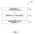
図2は、本発明の一実施形態によるボロンを用いて基板にドーピングする方法200を要約する。ボロン巨大分子を、202において、基板の表面中へと注入する。オクタデカボランまたはイコサボラン(B20H26)や、トリアンタボラン(B30Hx)や、サランタボラン(B40Hx)などであるがこれらに限定されない大量のボロンを含有する他の安定な巨大分子が、ある実施形態にとって有用である場合がある。上記の組み合わせまたは混合物を、やはり使用することができる。ボロンクラスタをイオン化させ、それらを基板に向けて導くために、プラズマイマージョン装置またはビーム注入装置を使用して、注入を実現することができる。注入エネルギーを調整するために、DCバイアスまたはRFバイアスを基板に印加することができる。
FIG. 2 summarizes a
基板表面の注入した部分を204において溶融する。オクタデカボランを注入した基板の処理のために適した溶融加熱プロセスを、任意の好都合なエネルギー源を使用して行うことができる。基板を、熱伝導によってまたは電磁放射による放射加熱によって加熱することができる。加熱した支持部上に基板を配置することができる、または可視放射光か、赤外放射光か、またはマイクロ波放射による照射を基板に行うことができる。加熱支持部を、その支持部内に埋め込んだ抵抗加熱を使用して、または熱流体を流すためにその支持部内に導管を設けることによって加熱することができる。放射光は、コヒーレントであってもインコヒーレントであってもよく、収束であっても非収束であってもよく、単色であっても多色であってもよく、または偏光であっても非偏光であってもよく、どのようにでもすることができる。放射光を、レーザや、フラッシュランプや、アークランプや、フィラメントランプの1つまたは複数の任意の組み合わせによって放出することができる。ある実施形態では、基板全体を同時に処理することができるが、別の実施形態では、基板の一部を連続して処理することができる。ある実施形態では、基板表面へのエネルギーの付与を改善し、基板を加熱するにつれて昇華によるボロンの損失を減少させるために、カーボン膜などのエネルギー吸収膜を、基板を覆って付けることができる。ある実施形態では、基板のバルクを冷たい支持部を使用して冷却しながら、基板表面を放射エネルギーにより加熱することができる。 The implanted portion of the substrate surface is melted at 204. A melt heating process suitable for processing a substrate implanted with octadecaborane can be performed using any convenient energy source. The substrate can be heated by thermal conduction or by radiant heating with electromagnetic radiation. The substrate can be placed on a heated support, or the substrate can be irradiated with visible radiation, infrared radiation, or microwave radiation. The heating support can be heated using resistance heating embedded in the support or by providing a conduit in the support for flowing a thermal fluid. The emitted light may be coherent or incoherent, may be converged or non-convergent, may be monochromatic or polychromatic, or polarized or non-polarized. It can be polarized and can be done in any way. The emitted light can be emitted by any combination of one or more of a laser, a flash lamp, an arc lamp, and a filament lamp. In some embodiments, the entire substrate can be processed simultaneously, while in other embodiments, a portion of the substrate can be processed sequentially. In some embodiments, an energy absorbing film, such as a carbon film, can be applied over the substrate to improve the application of energy to the substrate surface and reduce the loss of boron due to sublimation as the substrate is heated. In some embodiments, the substrate surface can be heated by radiant energy while the bulk of the substrate is cooled using a cold support.
オクタデカボランで注入した基板の部分を、注入した部分の溶融点の温度またはそれよりも高い温度に加熱する。ある実施形態では、基板のバルクが結晶質のままで注入した表面だけを溶融する。ある実施形態では、オクタデカボラン注入に付随するアモルファス化の程度のために、表面をアモルファス物質の溶融温度にまたはそれより高い温度に加熱すれば、十分である場合があり、そのアモルファス物質の溶融温度は、結晶質物質の溶融温度よりも一般に低い。シリコン基板を処理する実施形態に関して、1,200℃以上の温度が、表面のアモルファス化した部分を溶融するには十分である場合がある。アモルファスシリコンが結晶質シリコンよりも低い温度で溶融するために、アモルファス化した部分は、この温度で溶融するが、下にある結晶質相は溶融しない。熱応力による何らかの基板損傷を最小にするために、基板のバルクを中間の温度まで加熱することが、有利な場合がある。例示的な実施形態では、基板支持部は、500℃以上の温度に基板を加熱することができ、溶融温度まで基板の一部分を加熱するために、放射エネルギー源を使用することができる。溶融ゾーンの超高速加熱は、アモルファス相が結晶化する前にアモルファス相の溶融を実現するために一般に好まれている。ある実施形態では、10n秒と100n秒との間、例えば、20n秒などの、数ナノ秒から約200ナノ秒までのパルス持続時間を有するナノ秒パルスレーザを、アモルファス相を溶融させるために使用することができる。 The portion of the substrate implanted with octadecaborane is heated to a temperature at or above the melting point of the implanted portion. In some embodiments, only the implanted surface is melted while the bulk of the substrate remains crystalline. In some embodiments, due to the degree of amorphization associated with octadecaborane implantation, it may be sufficient to heat the surface to a temperature at or above the melting temperature of the amorphous material, and the melting of the amorphous material. The temperature is generally lower than the melting temperature of the crystalline material. For embodiments processing silicon substrates, temperatures above 1200 ° C. may be sufficient to melt the amorphized portions of the surface. Since amorphous silicon melts at a lower temperature than crystalline silicon, the amorphized part melts at this temperature, but the underlying crystalline phase does not melt. To minimize any substrate damage due to thermal stress, it may be advantageous to heat the bulk of the substrate to an intermediate temperature. In an exemplary embodiment, the substrate support can heat the substrate to a temperature of 500 ° C. or higher, and a radiant energy source can be used to heat a portion of the substrate to a melting temperature. Ultrafast heating of the melting zone is generally preferred to achieve melting of the amorphous phase before the amorphous phase crystallizes. In some embodiments, a nanosecond pulsed laser having a pulse duration between a few nanoseconds and about 200 nanoseconds, such as between 20 and 100 nanoseconds, eg, 20 nanoseconds, is used to melt the amorphous phase. can do.
溶融した後で、基板の溶融した部分は、206において再結晶化する。多くの実施形態では、注入したボロン原子を含む結晶格子の形成を促進させるやり方で、再結晶化を実行する。このやり方では、再結晶化は、アニーリングプロセスと類似している。結晶形成を促進させるために、通常の伝導冷却または放射冷却を介して実現されるはずの速度よりもゆっくりとした速度で溶融した部分を冷却することが、一般に好まれる。ある実施形態では、溶融に続いて、約1分と約10分との間、例えば、約3分などの、最大10分までの間、500℃以上で基板の温度を維持することが、有利な場合がある。別の実施形態では、基板表面の注入した部分を、約1℃/秒と約50℃/秒との間、例えば、約10℃/秒などの、約100℃/秒よりも早くない速度で冷却することが、有用である場合がある。さらに別の実施形態では、再結晶化を実現するために、ゆっくりとした冷却速度を、一定温度の期間と組み合わせることができる。 After melting, the molten portion of the substrate is recrystallized at 206. In many embodiments, recrystallization is performed in a manner that facilitates the formation of a crystal lattice that includes implanted boron atoms. In this way, recrystallization is similar to the annealing process. In order to promote crystal formation, it is generally preferred to cool the melted part at a slower rate than would be achieved through normal conduction or radiative cooling. In certain embodiments, following melting, it is advantageous to maintain the temperature of the substrate at 500 ° C. or higher for between about 1 and about 10 minutes, for example, up to 10 minutes, such as about 3 minutes. There is a case. In another embodiment, the implanted portion of the substrate surface is injected at a rate not between about 1 ° C./second and about 50 ° C./second, such as about 10 ° C./second, such as about 10 ° C./second. It may be useful to cool. In yet another embodiment, a slow cooling rate can be combined with a constant temperature period to achieve recrystallization.
本明細書中で説明したような注入しようとする基板に、プレクリーニングプロセスを行うことができる。溶液は、約0.1重量パーセントHFから約10.0重量パーセントHFの濃度を有することができ、約20℃から約30℃までの温度で使用することができる。例示的な実施形態では、溶液は、約0.5重量パーセントのHFおよび約25℃の温度を有する。別の例示的な一実施形態では、溶液は、約1.0重量パーセントのHFおよび約25℃の温度を有する。基板を、約10秒から約60秒までの持続期間、HF溶液形式に曝すことができる。HF溶液のエッチング作用によって、すべての望ましくない酸化物を基板から除去する。基板を溶液に短時間曝した後に、脱イオン水中でのリンスステップおよびベークステップが続く場合がある。ベークステップを、基板の表面からすべての残っている逃げやすい種を蒸発させるために選択した温度で、窒素ガスか、ヘリウムか、アルゴンなどの不活性雰囲気下で実行することができる。一実施形態では、基板を、約200℃と約600℃との間の温度に約60秒間曝露させることができる。 A pre-cleaning process can be performed on the substrate to be implanted as described herein. The solution can have a concentration of about 0.1 weight percent HF to about 10.0 weight percent HF and can be used at temperatures from about 20 ° C. to about 30 ° C. In an exemplary embodiment, the solution has about 0.5 weight percent HF and a temperature of about 25 ° C. In another exemplary embodiment, the solution has about 1.0 weight percent HF and a temperature of about 25 ° C. The substrate can be exposed to the HF solution format for a duration of about 10 seconds to about 60 seconds. All unwanted oxide is removed from the substrate by the etching action of the HF solution. A short exposure of the substrate to the solution may be followed by a rinse and bake step in deionized water. The bake step can be performed under an inert atmosphere such as nitrogen gas, helium or argon at a temperature selected to evaporate all remaining flammable species from the surface of the substrate. In one embodiment, the substrate can be exposed to a temperature between about 200 ° C. and about 600 ° C. for about 60 seconds.
本明細書中で説明したようなボロンを注入した基板に、アニールプロセスの後でストリッピングプロセスを行うことができ、すべての残存する高表面濃度のボロンを除去することができる。ある実施形態では、揮発性の水素化物を生成させるために、基板を水素含有ガスに曝露させる。ある実施形態では、水素含有ガスをプラズマとすることができる。例えば、基板の表面のところのドーパントを揮発性の水素化物へと変換するために、プラズマありまたはなしで、水素ガスまたはアンモニアを使用することができる。ボロンは反応して、ボランや、ジボランや、または別の揮発性ボランオリゴマーなどの、様々な揮発性ボロン水素化物を形成する場合がある。例示的な一実施形態では、ドーパントの表面濃度を低下させるために、約200℃などの、約100℃と約300℃との間の温度で、約15秒などの、約10秒と約30秒との間にわたって、基板を水素プラズマに曝露させることができる。水素プラズマを、その場でまたは遠く離れて発生させることができ、アルゴンまたはヘリウムなどの非反応性キャリアガスを伴う場合がある。キャリアガス流を、約1,500sccmなどの、約1,000sccmと約2,000sccmとの間の量で設定することができ、水素ガスのパルスを添加する。水素ガスのパルスを、約15秒などの、約10秒から約30秒の間隔にわたり、約300sccmなどの、約100sccmと約500sccmとの間の流量で供給することができる。曝露の後で、水素ガスを停止し、キャリアガスが、すべての残っている揮発性水素化物をチャンバからパージする。すべての残っている逃げやすい水素化物を除去するために、チャンバを、また、低い圧力に真空引きすることができる。 The substrate implanted with boron as described herein can be subjected to a stripping process after the annealing process to remove any remaining high surface concentration boron. In some embodiments, the substrate is exposed to a hydrogen-containing gas to produce volatile hydrides. In some embodiments, the hydrogen-containing gas can be a plasma. For example, hydrogen gas or ammonia can be used with or without plasma to convert the dopant at the surface of the substrate into volatile hydrides. Boron may react to form various volatile boron hydrides, such as borane, diborane, or another volatile borane oligomer. In one exemplary embodiment, to reduce the surface concentration of the dopant, at a temperature between about 100 ° C. and about 300 ° C., such as about 200 ° C., such as about 15 seconds, about 10 seconds and about 30 seconds. The substrate can be exposed to the hydrogen plasma for a period of seconds. The hydrogen plasma can be generated in situ or remotely and may be accompanied by a non-reactive carrier gas such as argon or helium. The carrier gas flow can be set at an amount between about 1,000 sccm and about 2,000 sccm, such as about 1,500 sccm, and a pulse of hydrogen gas is added. A pulse of hydrogen gas can be provided at a flow rate between about 100 sccm and about 500 sccm, such as about 300 sccm, over an interval of about 10 seconds to about 30 seconds, such as about 15 seconds. After exposure, the hydrogen gas is turned off and the carrier gas purges any remaining volatile hydride from the chamber. The chamber can also be evacuated to a lower pressure in order to remove any remaining flammable hydride.
図3は、本発明の別の一実施形態による方法300を要約する。基板を、302においてプロセシングチャンバ内に配置する。キャリアガスの流れを、304において設定する。キャリアガスを、ヘリウムか、アルゴンか、または窒素ガスなどの任意の非反応性ガスとすることができる。ある実施形態では、キャリアガス流量を、約2,000sccmと約4,000sccmとの間、例えば、3,000sccmなどの、約1,000sccmと約5,000sccmとの間とすることができる。ボロン巨大分子を包含する前駆体を、306において添加する。ボロン前駆体を、プロセシングチャンバの外でキャリアガスストリームに添加することができる、またはプロセシングチャンバに直接添加することができる。ボロン前駆体を、約200sccmと約400sccmとの間、例えば、約300sccmなどの、約100sccmと約500sccmとの間の流量で与えることができる。ボロン前駆体を蒸気状態に維持するために蒸発温度でまたはそれよりも高い温度で、ボロン前駆体を一般に与える。B18に関して、ボロン前駆体を、約250℃などの、約100℃と約400℃との間の温度で与えることができる。
FIG. 3 summarizes a
キャリアガスおよびボロン前駆体は、プロセシングチャンバの近くでまたはその中で、1つまたは複数のイオン化用ゾーン中へと流れ込む。308において、ボロン巨大分子を分解せずにボロン前駆体をイオン化させるために、イオン化用エネルギーを印加し、そのボロン前駆体はその後プロセシングチャンバ中へとガス分配器を介して出てくる。ある実施形態では、イオン化用エネルギーを、イオン化用ゾーンに電場をカップリングすることによって与えることができる。電場を、DCバイアスなどの静的なもの、またはRF出力の印加によって発生させるものなどの変化するものとすることができ、容量的手段または誘導的手段によってイオン化用ゾーンへとカップリングすることができる。一実施形態では、プロセシングチャンバからイオン化用ゾーンへとガスを運ぶための1つまたは複数の導管を用いて、誘導イオン化用ゾーンをプロセシングチャンバの外部に設ける。イオン化用ゾーンの周りに配置された1つまたは複数のトロイダル磁心を設けることによって、電場を各イオン化用ゾーンへとカップリングする。イオン化用ゾーン内部に電場を発生させるために、1つまたは複数のトロイダル磁心をRF出力により作動させる。大部分の実施形態に関して、イオン化用エネルギーを、約300Wなどの、約100Wと約500Wとの間の出力レベルで与えることができる。 The carrier gas and boron precursor flow into one or more ionization zones near or in the processing chamber. At 308, ionizing energy is applied to ionize the boron precursor without decomposing the boron macromolecule, which then exits through the gas distributor into the processing chamber. In certain embodiments, ionizing energy can be provided by coupling an electric field to the ionizing zone. The electric field can be static, such as DC bias, or variable, such as that generated by application of RF power, and can be coupled to the ionization zone by capacitive or inductive means. it can. In one embodiment, the induced ionization zone is provided external to the processing chamber using one or more conduits for carrying gas from the processing chamber to the ionization zone. An electric field is coupled to each ionization zone by providing one or more toroidal cores disposed around the ionization zone. To generate an electric field within the ionization zone, one or more toroidal cores are activated with RF power. For most embodiments, the ionization energy can be provided at a power level between about 100 W and about 500 W, such as about 300 W.
310において、基板表面に向けてイオン化したボロン巨大分子を加速させるために、電場を印加することができる。これを、基板支持部か、ガス分配器か、もしくは両方に印加するDCバイアスなどの静電場とすることができる、またはRF励振場などの変化する電場とすることができる。イオン化したボロン巨大分子が基板表面に向けて進むので、電場の印加は、イオン化したボロン巨大分子のエネルギーを調節するために使用する任意選択のステップである。ある実施形態は、イオンが表面に向けてドリフトすることを可能にすることができる。電場を使用する場合には、好ましくは、約100Wなどの、約50Wと約500Wとの間の出力レベルで印加する弱い電場である。ある実施形態では、イオン化したボロン巨大分子は、約100eVと約2,000eVとの間の運動エネルギーで基板表面に向けて進む。個々の実施形態は、これら2つの値の間の運動エネルギーの任意の特定の値または範囲でイオンにエネルギーを与えることができる。1つの実施形態は、やはり、この範囲内のエネルギーの分布があるイオンを取り上げることができる。例えば、イオン化したボロン巨大分子の第1の部分は、熱勾配か、圧力勾配か、もしくは電気的勾配、またはこれらの変動のために、イオン化したボロン巨大分子の第2の部分よりも大きな運動エネルギーを有する場合がある。 At 310, an electric field can be applied to accelerate the ionized boron macromolecule toward the substrate surface. This can be an electrostatic field such as a DC bias applied to the substrate support, the gas distributor, or both, or it can be a changing electric field such as an RF excitation field. As the ionized boron macromolecule travels toward the substrate surface, the application of an electric field is an optional step used to adjust the energy of the ionized boron macromolecule. Certain embodiments can allow ions to drift toward the surface. If an electric field is used, it is preferably a weak electric field applied at a power level between about 50 W and about 500 W, such as about 100 W. In some embodiments, the ionized boron macromolecule travels toward the substrate surface with a kinetic energy between about 100 eV and about 2,000 eV. Individual embodiments can energize ions with any particular value or range of kinetic energy between these two values. One embodiment can still pick up ions with a distribution of energy within this range. For example, the first portion of the ionized boron macromolecule has a greater kinetic energy than the second portion of the ionized boron macromolecule due to thermal gradients, pressure gradients, or electrical gradients, or variations thereof. May have.
イオン化したボロン巨大分子は、312において基板支持部上に配置された基板に衝突し、基板表面中へと注入される。巨大分子は、一般に、その巨大分子が衝突するときに基板表面の結晶基質を破壊するために十分な運動エネルギーを運び、表面をアモルファス化する。それに加えて、ボロン巨大分子が基板表面中へと押し入るときに、ボロン巨大分子がばらばらになる。その小部分は、一般に、アモルファス化プロセスのために主巨大分子から横方向にそれ、比較的急峻な注入したままの状態の濃度プロファイルを結果としてもたらす。ある実施形態では、注入したままの状態のボロンの最大濃度を、表面の下方約10nmなどの、表面の下方約5nmと約15nmとの間とすることができ、その深さのところで約1019cm−3と約1021cm−3との間とすることができる。注入したままの状態の濃度は、一般に、注入エネルギーに応じて2〜20nm/decのレートで下がる。注入層は、一般に、約50nm厚などの、約30nm厚と約150nm厚との間である。結果として生ずる注入層は、その層全体に分散されたボロン原子または各々が2個から4個のボロン原子の小さなボロンクラスタがある状態で、ボロン巨大分子の作用によって完全にアモルファス化される。 The ionized boron macromolecule collides with the substrate disposed on the substrate support at 312 and is injected into the substrate surface. Macromolecules generally carry sufficient kinetic energy to break down the crystalline substrate on the substrate surface when the macromolecules collide, making the surface amorphous. In addition, when the boron macromolecules push into the substrate surface, the boron macromolecules fall apart. The small portion generally deviates from the main macromolecule laterally due to the amorphization process, resulting in a relatively steep as-implanted concentration profile. In certain embodiments, the maximum concentration of as-implanted boron can be between about 5 nm and about 15 nm below the surface, such as about 10 nm below the surface, at about 10 19 at that depth. It can be between cm −3 and about 10 21 cm −3 . The concentration of the as-implanted state generally decreases at a rate of 2 to 20 nm / dec depending on the implantation energy. The injection layer is generally between about 30 nm and about 150 nm thick, such as about 50 nm thick. The resulting implanted layer is fully amorphized by the action of boron macromolecules with boron atoms dispersed throughout the layer or small boron clusters of 2 to 4 boron atoms each.
314において、加熱エネルギーを、1つまたは複数の注入した部分に与える。注入した区域の温度を溶融点またはそれよりも高くまで上昇させるように、加熱エネルギーを選択する。加熱エネルギーを、任意の好都合な方法によって与えることができる。例えば、電磁エネルギーまたは放射エネルギーを、注入した区域の一部を溶融させるために注入した区域に向けて投射することができる。それに加えて、注入した区域か、溶融させるべき注入した区域を含有する基板の区域か、または基板全体をプレヒートするために、バックグラウンド加熱を与えることができる。例えば、加熱した基板支持部は、基板の温度を約400℃と約700℃との間まで上昇させるために基板に伝導加熱エネルギーを与えることができ、その温度に維持すると同時に追加の加熱エネルギーを与えることによって個々の注入した区域を溶融させる。注入した区域を溶融させるための放射エネルギーを、レーザか、加熱ランプか、フラッシュランプか、またはその他によって放出することができ、パルスであっても連続であってもよく、コヒーレントであってもインコヒーレントであってもよく、単色であっても多色であってもよく、偏光であっても非偏光であってもよく、どのようにでもすることができる。基板の一部を連続して照射することができる、または基板全体を同時に照射することができる。注入した部分を、実施形態に応じて、約1,100℃と約1,400℃との間の温度まで加熱することができる。アモルファス化したシリコンの溶融は、一般に結晶質シリコンの溶融よりも低い温度で生じ、そのため基板材料が主にシリコンである実施形態では、約1,200℃に注入した部分を加熱することを考慮することができる。溶融温度を、下にある結晶質層を溶融させずにアモルファス層を溶融させるように選択する。早い速度で溶融させるべき部分を加熱することが、一般に望ましく、その結果、熱が基板材料によって伝導で逃げることができるよりも早く、アモルファス部分を加熱し、アモルファス部分が再結晶化できる前に溶融させる。アモルファスシリコンがそれ自体の溶融点近くまでゆっくりと加熱されるときには、アモルファスシリコンは、固相エピタキシを受け、より高い溶融点の結晶質シリコンへと変換する。超急速加熱は、アモルファス部分が再結晶化できる前にアモルファス部分を溶融させることができる。 At 314, heating energy is applied to one or more implanted portions. The heating energy is selected so that the temperature of the injected area is raised to the melting point or higher. Heating energy can be provided by any convenient method. For example, electromagnetic or radiant energy can be projected toward the injected area to melt a portion of the injected area. In addition, background heating can be provided to preheat the implanted area, the area of the substrate containing the implanted area to be melted, or the entire substrate. For example, a heated substrate support can provide conductive heating energy to the substrate to raise the temperature of the substrate to between about 400 ° C. and about 700 ° C. while maintaining that temperature while providing additional heating energy. By melting, the individual injected areas are melted. The radiant energy for melting the injected area can be emitted by a laser, heating lamp, flash lamp, or others, which can be pulsed, continuous, or coherent. It may be coherent, monochromatic or polychromatic, polarized or non-polarized, and can be done in any way. A portion of the substrate can be irradiated continuously, or the entire substrate can be irradiated simultaneously. The injected portion can be heated to a temperature between about 1,100 ° C. and about 1,400 ° C., depending on the embodiment. Amorphized silicon melting generally occurs at a lower temperature than crystalline silicon melting, so in embodiments where the substrate material is primarily silicon, consider heating the portion implanted at about 1200 ° C. be able to. The melting temperature is selected to melt the amorphous layer without melting the underlying crystalline layer. It is generally desirable to heat the part to be melted at a fast rate, so that the amorphous part is heated and melted before the amorphous part can be recrystallized faster than heat can be conducted away by the substrate material. Let As amorphous silicon is slowly heated to near its own melting point, the amorphous silicon undergoes solid phase epitaxy and transforms into higher melting point crystalline silicon. Ultra-rapid heating can melt the amorphous portion before it can be recrystallized.
316において、注入表面の溶融した部分の温度を、一定時間にわたり溶融温度よりも高く維持して、残っているボロンの小部分の完全な分解および最大濃度層の外へのボロンのある程度の拡散を可能にする。ナノ秒パルスレーザを使用する大部分の実施形態は、数10ナノ秒から数100ナノ秒の溶融持続時間を考慮する。ある実施形態では、しかしながら、溶融持続時間を、約10m秒などの、数ミリ秒と約0.5秒との間とすることができる。 At 316, the temperature of the melted portion of the implantation surface is maintained above the melting temperature for a period of time to achieve complete decomposition of the remaining small portion of boron and some diffusion of boron out of the maximum concentration layer. enable. Most embodiments using nanosecond pulsed lasers consider melt durations from tens of nanoseconds to hundreds of nanoseconds. In certain embodiments, however, the melt duration can be between a few milliseconds and about 0.5 seconds, such as about 10 milliseconds.
318において、基板表面を再結晶化させるまたは再固化させるために、基板表面の加熱した部分を制御した速度で冷却する。一般には、この冷却速度は、制御した再結晶化を可能にするために、単純に加熱装置の電源を切ることを介して起きるはずのものよりもゆっくりとしている。この制御した再結晶化プロセスは、ボロンドーパント原子を結晶格子位置に動かし、所定の位置に凍結させることによって、注入したボロン巨大分子に由来するボロンドーパント原子を効率的に活性化させる。ある実施形態では、加熱源のエネルギー−時間プロファイルを調節することによって溶融させた注入物の冷却速度を制御するために、加熱エネルギーを溶融させた注入区域に与えることができる。例えば、ナノ秒レーザのパルスのプロファイルを、パルス修正光学系を使用して調節することができる、または1つもしくは複数のフラッシュランプに印加する放電電圧パルスの形を調節することができる。上に説明した方法のいずれかによれば、加熱エネルギーを電磁エネルギーまたは放射エネルギーとすることができる。別の実施形態では、再結晶化プロセスを成し終えるためのある一定時間にわたって中間の温度で基板の温度を維持するために、加熱エネルギーを基板全体に与えることができる。例えば、約1分と約10分との間にわたり、約400℃と約700℃との間で基板温度を維持することによって、基板を再結晶化させることができる。例えば、一実施形態では、基板を、約60秒間、約500℃で基板温度を維持することによって再結晶化させることができる。制御した冷却プロセスは、基板表面から結晶欠陥を消去し、ドーパントを分布させ、ドーパントを活性化させるように、基板表面をアニールする。 At 318, the heated portion of the substrate surface is cooled at a controlled rate to recrystallize or resolidify the substrate surface. In general, this cooling rate is slower than that which would occur through simply turning off the heating device to allow controlled recrystallization. This controlled recrystallization process efficiently activates boron dopant atoms derived from implanted boron macromolecules by moving boron dopant atoms to crystal lattice positions and freezing them in place. In certain embodiments, heating energy can be applied to the molten injection zone to control the cooling rate of the molten injection by adjusting the energy-time profile of the heating source. For example, the pulse profile of a nanosecond laser can be adjusted using pulse correction optics, or the shape of the discharge voltage pulse applied to one or more flash lamps can be adjusted. According to any of the methods described above, the heating energy can be electromagnetic energy or radiant energy. In another embodiment, heating energy can be applied to the entire substrate to maintain the temperature of the substrate at an intermediate temperature for a period of time to complete the recrystallization process. For example, the substrate can be recrystallized by maintaining the substrate temperature between about 400 ° C. and about 700 ° C. for between about 1 minute and about 10 minutes. For example, in one embodiment, the substrate can be recrystallized by maintaining the substrate temperature at about 500 ° C. for about 60 seconds. A controlled cooling process anneals the substrate surface to erase crystal defects from the substrate surface, distribute the dopant, and activate the dopant.
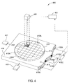
図4は、本発明の実施形態を実行するために使用することができるアニールシステム400を概略的に図示する。アニールシステム400は、アニール領域412内のある所望の領域を優先的に溶融させるために、基板410の所定の領域、すなわちアニール領域412上にある量のエネルギーを投射することに適合するエネルギー源420を備える。
FIG. 4 schematically illustrates an
一例では、図4に示したように、アニール領域412などの基板410の1つだけの所定の領域を、任意の所与の時刻においてエネルギー源420からの放射に曝露させる。基板410上の別の領域をエネルギー源420に逐次的に曝露させることができるように、基板410が、エネルギー源420に対して相対的に動く。
In one example, as shown in FIG. 4, only one predetermined region of
本発明の一態様では、基板410の所望の領域の優先的な溶融を生じさせるために、基板410の複数の区域を、エネルギー源420から放出される所望の量のエネルギーに逐次的に曝露させる。
In one aspect of the present invention, multiple areas of the
一般的に、(例えば、従来型のX/Yステージ、精密ステージを使用して)エネルギー源420の出力域に対して相対的に基板410を移動させることによって、および/または基板410に対して相対的にエネルギー源420の出力域を移動させることによって、基板410の表面上の区域を逐次的に曝露させることができる。
Generally, by moving the
基板410の全体の温度を制御するように構成された熱交換機器415上に、基板410を設置することができる。基板410の動きおよび位置を制御するように構成され、別の精密ステージ(図示せず)の一部である場合がある、1つまたは複数の従来型の電気式アクチュエータ417(例えば、リニアモータや、送りネジや、サーボモータ)上に、熱交換機器415を設置することができる。基板410を支持し設置するために使用することができる従来型の精密ステージおよび熱交換機器415を、Rohnert Park、CaliforniaのParker Hannifin Corporationから購入することができる。
The
一態様では、アニール領域412を、基板410の表面上に形成されるダイ413(例えば、40個のダイが図4に示されている)または半導体デバイス(例えば、メモリチップ)のサイズと一致するような大きさにする。一態様では、アニール領域412の境界を、各ダイ413の境界を画定する「カーフ」ラインまたは「スクライブ」ライン410A内にぴったりと合うように位置合わせし、大きさを合わせる。
In one aspect, the
スクライブラインまたはカーフライン410Aなどのダイ413間に自然に生じる使用されない空間/境界内だけでアニール領域412が重なるようにアニール領域412を逐次的に並べることは、デバイスを基板410上に形成する区域内でエネルギーが重複する困った状態を低減し、従って、重なりのあるアニール領域412間でのプロセス結果における変動を低減する。
Sequential alignment of
一実施形態では、アニーリングプロセスを実行することに先立って、アニール領域412をダイ413に適切に位置合わせすることができるように、基板410の表面上に典型的に見出されるアライメントマークおよび他の従来技術を使用して、基板410をエネルギー源420の出力域に位置合わせする。
In one embodiment, prior to performing the annealing process, alignment marks and other conventional ones typically found on the surface of the
基板表面のある所望の領域を優先的に溶融させるために、エネルギー源420は、電磁エネルギーを放出することに一般に適合する。典型的な電磁エネルギー源は、光放射源(例えば、レーザ)や、電磁ビーム源や、イオンビーム源、および/またはマイクロ波エネルギー源を含むが、これらに限定されない。
In order to preferentially melt certain desired areas of the substrate surface, the
一般的に、熱交換機器415を含有するプロセシングチャンバ(図示せず)の囲まれたプロセシング環境(図示せず)内に、基板410を置く。加工処理中に基板410がその中に存在するプロセシング環境を、真空にすることができる、または酸素などの加工処理中には望まれないガスの低い分圧を有する不活性ガスを含有させることができる。
In general, the
一実施形態では、図4に図示した、熱交換機器415の基板支持表面416と熱接触させて基板410の表面を置くことによって、熱加工処理中に基板410の温度を制御することが望ましいことがある。熱交換機器415は、アニーリングプロセスに先立ってまたはその間に基板410を加熱するおよび/または冷却することに一般に適合している。この構成では、Santa Clara、CaliforniaのApplied Materials,Inc.から入手可能な従来型の基板ヒータなどの、熱交換機器415を、基板410のアニール領域のポストプロセシング特性を向上させるために使用することができる。
In one embodiment, it may be desirable to control the temperature of the
一実施形態では、溶融温度に達するまでの必要なエネルギーが最小になるように、アニーリングプロセスを実行することに先立って、基板をプレヒートすることができ、そのプレヒートは、基板410の急速加熱および冷却に起因して誘起される何らかの応力を低減させることができ、また、基板410の再固化される区域内の欠陥密度をおそらく低減させることができる。一態様では、熱交換機器415は、基板支持表面416上に配置された基板410を加熱することに適合した抵抗加熱素子415Aおよび温度コントローラ415Cを含有する。温度コントローラ415Cは、コントローラ421と通信する。
In one embodiment, the substrate can be preheated prior to performing the annealing process so that the required energy to reach the melting temperature is minimized, which preheat and cool the
一態様では、基板を約20℃と約750℃との間の温度にプレヒートすることが望ましい場合がある。基板がシリコン含有材料から形成される一実施形態では、基板を約20℃と約500℃との間の温度にプレヒートすることが望ましい場合がある。基板がシリコン含有材料から形成される別の一実施形態では、基板を約200℃と約480℃との間の温度にプレヒートすることが望ましい場合がある。基板がシリコン含有材料から形成される別の一実施形態では、基板を約250℃と約300℃との間の温度にプレヒートすることが望ましい場合がある。 In one aspect, it may be desirable to preheat the substrate to a temperature between about 20 ° C. and about 750 ° C. In one embodiment where the substrate is formed from a silicon-containing material, it may be desirable to preheat the substrate to a temperature between about 20 ° C and about 500 ° C. In another embodiment where the substrate is formed from a silicon-containing material, it may be desirable to preheat the substrate to a temperature between about 200 ° C. and about 480 ° C. In another embodiment where the substrate is formed from a silicon-containing material, it may be desirable to preheat the substrate to a temperature between about 250 ° C and about 300 ° C.
別の一実施形態では、アニーリングプロセス中に基板に与えられるエネルギーに起因する何らかの拡散を低減させるため、および/または加工処理中に様々な領域のアモルファス化を増大させるために溶融の後の再成長速度を増大させるために、加工処理中に基板を冷却することが望ましい場合がある。1つの構成では、熱交換機器415は、基板支持表面416上に配置された基板を冷却することに適合した1つまたは複数の流体チャネル415Bおよび低温冷却装置415Dを含有する。一実施形態では、コントローラ421と通信する従来型の低温冷却装置415Dは、1つまたは複数の流体チャネル415Bを介して冷却流体を配送することに適合している。一態様では、基板を約−240℃と約20℃との間の温度に冷却することが望ましい場合がある。
In another embodiment, regrowth after melting to reduce any diffusion due to energy imparted to the substrate during the annealing process and / or to increase amorphization of various regions during processing. It may be desirable to cool the substrate during processing to increase speed. In one configuration, the
パルスレーザアニールプロセス中に、基板の複数の部分がエネルギー源に逐次的に向けられるように、加工処理されるべき基板は、エネルギー源に対して相対的に動く。相対的な動きを、ステッピング動作とすることができる。例えば、基板上の第1の区域がエネルギー源と位置合わせされるように、基板を、第1の位置に動かし、維持することができる。エネルギー源は、次に、基板上の第1の区域に向けて所望の量のエネルギーを投射する。基板を、次に、エネルギー源による第2の区域へ第2の位置に動かす。エネルギーが所望の区域に正確にかつ均一に投射されるように、エネルギー源が基板にエネルギーを投射するときに、基板とエネルギー源との間の相対的な動きを、一時的に停止する。しかしながら、このステッピング動作は、ステップ毎に加速することおよび減速することを伴い、その動作はプロセスを著しく遅くする。 During the pulsed laser annealing process, the substrate to be processed moves relative to the energy source so that portions of the substrate are sequentially directed to the energy source. The relative movement can be a stepping operation. For example, the substrate can be moved and maintained in the first position such that the first area on the substrate is aligned with the energy source. The energy source then projects a desired amount of energy toward a first area on the substrate. The substrate is then moved to a second position to a second zone with an energy source. The relative movement between the substrate and the energy source is temporarily stopped when the energy source projects energy onto the substrate so that the energy is accurately and uniformly projected onto the desired area. However, this stepping operation involves accelerating and decelerating step by step, and that operation significantly slows the process.
図5は、アレイに配列された40個の正方形をしたダイ413を含有する基板410の上面図を概略的に図示する。ダイ413は、スクライブライン410Aによって指し示される区域によって互いに分離される。エネルギー投射領域520Aは、その区域全体にわたり(図4に示した)エネルギー源420がエネルギーパルスを放出するように適合する区域を指す。一般的に、エネルギー投射領域520Aは、各ダイ413の区域に等しい区域またはそれよりも大きな区域をカバーすることができるが、各ダイ413の区域プラス周囲のスクライブライン410Aの区域よりも小さく、その結果、エネルギー投射領域520A内に放出されるエネルギーパルスがダイ413を完全にカバーするが隣のダイ413とは重ならない。
FIG. 5 schematically illustrates a top view of a
基板表面全体にわたり広がる複数のダイ413上にアニーリングプロセスを実行するために、基板および/またはエネルギー源420の出力域は、各ダイに関連して設置され、位置合わせされる必要がある。一実施形態では、曲線520Bは、アニーリングプロセスが基板の表面上の各ダイ413に実行されるので一連のアニーリングプロセス中の、基板410のダイ413とエネルギー源420のエネルギー投射領域520Aとの間の相対的な動きを図示する。一実施形態では、動きが曲線520Bに従うように、x方向およびy方向に基板を移動することによって、相対的な動きを実現することができる。別の一実施形態では、静止している基板410に対して相対的にエネルギー投射領域520Aを動かすことによって、相対的な動きを実現することができる。
In order to perform the annealing process on a plurality of dies 413 extending across the substrate surface, the output area of the substrate and / or
それに加えて、ダイの固有の配列に応じて、スループットおよびプロセス品質を最適化するために、520Bとは異なる経路を使用することができる。 In addition, depending on the unique arrangement of dies, a different path than 520B can be used to optimize throughput and process quality.
一実施形態では、アニーリングプロセス中に、基板410は、図5の曲線520Bによって示されるように、エネルギー投射領域520Aに対して相対的に動く。特定のダイ413がエネルギー投射領域520A内に設置され位置合わせされると、ダイ413が、特定のアニールプロセスレシピに従って所定の持続時間にわたりある量のエネルギーに曝露されるように、エネルギー源420は、基板410に向けてエネルギーのパルスを投射する。基板410とエネルギー投射領域520Aとの間の相対的な動きが、各ダイ413全体にわたって何らかの「ブラー(blur)」、すなわち、不均一なエネルギー分布、を引き起こさず、基板に損傷を引き起こすことのないようにエネルギー源420からのパルスエネルギーの持続時間は、典型的には十分に短い。
In one embodiment, during the annealing process, the
注入した領域の急速繰り返し加熱および冷却を伴うサブメルトアニールプロセスを使用して、B18イオンを注入した基板をアニールすることができる。図6は、別の一実施形態による方法600を要約した流れ図である。602において、いずれかの所望の実施形態に従って、基板表面にボロン巨大分子を注入する。604において、注入した部分を、電磁エネルギーのパルスに曝露させることによってアニールする。電磁エネルギーのパルスは、繰り返し注入した部分を急速に加熱し冷却して、基板をアニールする。
Using sub melt annealing process with rapid repetitive heating and cooling of the injected region, the substrate injected with B 18 ions may be annealed. FIG. 6 is a flow diagram summarizing a
一実施形態では、電磁エネルギーのパルスは、実質的に同じエネルギーフラックスで同じ持続時間の電磁エネルギーの少なくとも約30パルスを包含する。一実施形態では、パルスの数を、約30パルスと約100,000パルスとの間、または約50パルスと約10,000パルスとの間、または約100パルスと約1,000パルスとの間、または約200パルスと約500パルスとの間などの、少なくとも約30パルス、または少なくとも約50パルス、または少なくとも約100パルスとすることができる。一実施形態では、各パルスのエネルギーフラックスは、約0.2J/cm2と約1.0J/cm2との間、例えば、約0.25J/cm2などの、約0.1J/cm2と約2.0J/cm2との間である。一実施形態では、パルスはレーザ光を包含する。各パルスは、約10n秒と約100n秒との間、例えば、20n秒などの、約1n秒と約10μ秒との間の持続時間を有することができる。必要とされるパルスの数は、一般に、各パルスのフルエンスおよび持続時間に逆比例する。 In one embodiment, the pulses of electromagnetic energy include at least about 30 pulses of electromagnetic energy of substantially the same energy flux and the same duration. In one embodiment, the number of pulses is between about 30 and about 100,000 pulses, or between about 50 and about 10,000 pulses, or between about 100 and about 1,000 pulses. Or at least about 30 pulses, such as between about 200 and about 500 pulses, or at least about 50 pulses, or at least about 100 pulses. In one embodiment, the energy flux of each pulse is between about 0.2 J / cm 2 and about 1.0 J / cm 2 , for example about 0.1 J / cm 2, such as about 0.25 J / cm 2. And about 2.0 J / cm 2 . In one embodiment, the pulse includes laser light. Each pulse can have a duration of between about 1 nsec and about 10 μsec, such as between about 10 nsec and about 100 nsec, eg, 20 nsec. The number of pulses required is generally inversely proportional to the fluence and duration of each pulse.
電磁エネルギーの各パルスは、基板のエネルギーを与えた区域内にマイクロアニールサイクルを実現する。細分化されていないボロンクラスタは、壊され、個々のボロン原子およびシリコン原子を、各パルスによって単位格子寸法の数分の1動かす。結晶格子位置を占有するボロン原子およびシリコン原子は、それらをその場所から動かすために十分なエネルギーを各パルスから受け取らないが、結晶格子配置間の空間を占めるこれらの原子は、占有されていない格子位置に向けて徐々に動く。パルス間には入射エネルギーフラックスは低下して、次のパルスが放出される前に各パルスからのエネルギーが結晶格子を通って消散することを可能にする。一実施形態では、入射エネルギーフラックスがパルス間にはゼロ近くにまで低下することがある。別の一実施形態では、入射エネルギーフラックスは低下して、正味のエネルギーフラックスをアニール帯の外にさせる。従って、標準的なサブメルト技術が20μ秒以上継続する放射光のスパイクにボロンドープした基板を曝露させることを必要とするが、繰り返しの短パルスは、はるかに短い合計持続時間および低い出力必要量でアニールプロセスを実現することができる。各パルスの持続時間に対して相対的に各パルス間の時間を、約100%と約150%との間、例えば、約125%などの、約50%と約200%との間とすることができる。パルス持続時間の約100%より短い残りの期間は、次のパルスが始まる前に、注入した領域の正味のエネルギーバランスがパルス中に受けるピークエネルギー密度よりも低いゼロでないレベルにまで低下することを可能にする。パルス持続時間の約125%よりも長い残りの期間は、正味のエネルギーバランスが次のパルスに先立って休止状態にまで戻ることを可能にする。 Each pulse of electromagnetic energy implements a microanneal cycle within the energized area of the substrate. Non-subdivided boron clusters are broken and individual boron atoms and silicon atoms are moved by a fraction of the unit cell size with each pulse. Boron and silicon atoms that occupy crystal lattice positions do not receive enough energy from each pulse to move them from that location, but those atoms that occupy the space between crystal lattice configurations are not occupied Move gradually toward the position. Between pulses, the incident energy flux decreases, allowing energy from each pulse to dissipate through the crystal lattice before the next pulse is emitted. In one embodiment, the incident energy flux may drop to near zero between pulses. In another embodiment, the incident energy flux is reduced, causing the net energy flux to be out of the anneal zone. Thus, while standard submelt techniques require exposing the boron-doped substrate to a spike of radiation that lasts for more than 20 μs, repeated short pulses anneal with a much shorter total duration and lower power requirements. Process can be realized. Relative to the duration of each pulse, the time between each pulse should be between about 100% and about 150%, for example between about 50% and about 200%, such as about 125%. Can do. The remaining period, shorter than about 100% of the pulse duration, will reduce the net energy balance of the implanted region to a non-zero level lower than the peak energy density experienced during the pulse before the next pulse begins. enable. The remaining period, longer than about 125% of the pulse duration, allows the net energy balance to return to rest before the next pulse.
一例では、500eVの等価ボロンイオンエネルギーで2×1015cm−2のドーズにまでB18イオンを、基板に注入した。約1.4μ秒の合計持続時間にわたり532nmの波長で0.234J/cm2を放出する20n秒レーザによる30パルスの後で、RSは、約500Ωであった。約45μ秒の持続時間にわたる1000パルスの後では、RSは、約400Ωであった。 In one example, B 18 ions were implanted into the substrate to a dose of 2 × 10 15 cm −2 with an equivalent boron ion energy of 500 eV. After 30 pulses with a 20 nsec laser emitting 0.234 J / cm 2 at a wavelength of 532 nm for a total duration of about 1.4 μsec, R S was about 500Ω. After 1000 pulses over a duration of about 45 μs, R S was about 400Ω.
別の一例では、同様のドーズおよびイオンエネルギーでB18イオンを基板に注入した。約13.5μ秒の合計持続時間にわたり532nmの波長で0.234J/cm2を放出する20n秒レーザによる300パルスの後で、約147Åの深さで、約5Å/decのその深さにおける濃度プロファイルで、1019cm−3のボロンイオン濃度が認められた。 In another example, B 18 ions were implanted into the substrate with similar dose and ion energy. After 300 pulses with a 20 nsec laser emitting 0.234 J / cm 2 at a wavelength of 532 nm for a total duration of about 13.5 μsec, at a depth of about 147 mm and a concentration at that depth of about 5 mm / dec In the profile, a boron ion concentration of 10 19 cm −3 was observed.
上記は本発明の実施形態に向けられているが、本発明の別の実施形態およびさらなる実施形態を、本発明の基本的な範囲から乖離せずに考案することができ、本発明の範囲は、下記の特許請求の範囲によって決められる。 While the above is directed to embodiments of the invention, other and further embodiments of the invention may be devised without departing from the basic scope thereof. Is determined by the following claims.
Claims (15)
前記基板の表面中へとボロン巨大分子を注入するステップと、
前記ボロン巨大分子を注入した前記基板の前記表面を溶融するステップと、
前記ボロン巨大分子を注入した前記基板の前記表面を再固化させるステップと、
前記基板の前記表面をアニールするステップと
を含む方法。 A method of processing a substrate, comprising:
Injecting boron macromolecules into the surface of the substrate;
Melting the surface of the substrate implanted with the boron macromolecule;
Resolidifying the surface of the substrate implanted with the boron macromolecule;
Annealing the surface of the substrate.
前記基板の表面中へとオクタデカボランを注入するステップと、
前記基板の注入した領域を繰り返して加熱し冷却することによって前記注入した領域をアニールするステップと
を含む方法。 A method of processing a substrate, comprising:
Injecting octadecaborane into the surface of the substrate;
Annealing the implanted region by repeatedly heating and cooling the implanted region of the substrate.
Applications Claiming Priority (3)
| Application Number | Priority Date | Filing Date | Title |
|---|---|---|---|
| US10013408P | 2008-09-25 | 2008-09-25 | |
| US61/100,134 | 2008-09-25 | ||
| PCT/US2009/057708 WO2010036621A2 (en) | 2008-09-25 | 2009-09-21 | Defect-free junction formation using octadecaborane self-amorphizing implants |
Publications (2)
| Publication Number | Publication Date |
|---|---|
| JP2012503886A true JP2012503886A (en) | 2012-02-09 |
| JP2012503886A5 JP2012503886A5 (en) | 2012-11-08 |
Family
ID=42038098
Family Applications (1)
| Application Number | Title | Priority Date | Filing Date |
|---|---|---|---|
| JP2011529150A Pending JP2012503886A (en) | 2008-09-25 | 2009-09-21 | Defect-free junction formation using octadecaborane self-amorphizing implant species |
Country Status (5)
| Country | Link |
|---|---|
| US (1) | US8067302B2 (en) |
| JP (1) | JP2012503886A (en) |
| KR (1) | KR20110082007A (en) |
| CN (1) | CN102165561A (en) |
| WO (1) | WO2010036621A2 (en) |
Cited By (2)
| Publication number | Priority date | Publication date | Assignee | Title |
|---|---|---|---|---|
| JP2013235992A (en) * | 2012-05-10 | 2013-11-21 | Ulvac Japan Ltd | Ion implantation method |
| WO2019244665A1 (en) * | 2018-06-22 | 2019-12-26 | 住友重機械工業株式会社 | Laser annealing method for semiconductor device, semiconductor device, laser annealing method, control device for laser annealing device, and laser annealing device |
Families Citing this family (48)
| Publication number | Priority date | Publication date | Assignee | Title |
|---|---|---|---|---|
| US8421162B2 (en) | 2009-09-30 | 2013-04-16 | Suvolta, Inc. | Advanced transistors with punch through suppression |
| US8273617B2 (en) | 2009-09-30 | 2012-09-25 | Suvolta, Inc. | Electronic devices and systems, and methods for making and using the same |
| US8530286B2 (en) | 2010-04-12 | 2013-09-10 | Suvolta, Inc. | Low power semiconductor transistor structure and method of fabrication thereof |
| US8569128B2 (en) | 2010-06-21 | 2013-10-29 | Suvolta, Inc. | Semiconductor structure and method of fabrication thereof with mixed metal types |
| US8759872B2 (en) | 2010-06-22 | 2014-06-24 | Suvolta, Inc. | Transistor with threshold voltage set notch and method of fabrication thereof |
| US8404551B2 (en) | 2010-12-03 | 2013-03-26 | Suvolta, Inc. | Source/drain extension control for advanced transistors |
| US8461875B1 (en) | 2011-02-18 | 2013-06-11 | Suvolta, Inc. | Digital circuits having improved transistors, and methods therefor |
| US8525271B2 (en) | 2011-03-03 | 2013-09-03 | Suvolta, Inc. | Semiconductor structure with improved channel stack and method for fabrication thereof |
| US8748270B1 (en) | 2011-03-30 | 2014-06-10 | Suvolta, Inc. | Process for manufacturing an improved analog transistor |
| US8796048B1 (en) | 2011-05-11 | 2014-08-05 | Suvolta, Inc. | Monitoring and measurement of thin film layers |
| US8999861B1 (en) | 2011-05-11 | 2015-04-07 | Suvolta, Inc. | Semiconductor structure with substitutional boron and method for fabrication thereof |
| US8811068B1 (en) | 2011-05-13 | 2014-08-19 | Suvolta, Inc. | Integrated circuit devices and methods |
| US8569156B1 (en) | 2011-05-16 | 2013-10-29 | Suvolta, Inc. | Reducing or eliminating pre-amorphization in transistor manufacture |
| US8735987B1 (en) | 2011-06-06 | 2014-05-27 | Suvolta, Inc. | CMOS gate stack structures and processes |
| US8995204B2 (en) | 2011-06-23 | 2015-03-31 | Suvolta, Inc. | Circuit devices and methods having adjustable transistor body bias |
| US8629016B1 (en) | 2011-07-26 | 2014-01-14 | Suvolta, Inc. | Multiple transistor types formed in a common epitaxial layer by differential out-diffusion from a doped underlayer |
| US8748986B1 (en) | 2011-08-05 | 2014-06-10 | Suvolta, Inc. | Electronic device with controlled threshold voltage |
| WO2013022753A2 (en) | 2011-08-05 | 2013-02-14 | Suvolta, Inc. | Semiconductor devices having fin structures and fabrication methods thereof |
| US8614128B1 (en) | 2011-08-23 | 2013-12-24 | Suvolta, Inc. | CMOS structures and processes based on selective thinning |
| US8645878B1 (en) | 2011-08-23 | 2014-02-04 | Suvolta, Inc. | Porting a circuit design from a first semiconductor process to a second semiconductor process |
| US8713511B1 (en) | 2011-09-16 | 2014-04-29 | Suvolta, Inc. | Tools and methods for yield-aware semiconductor manufacturing process target generation |
| US9236466B1 (en) | 2011-10-07 | 2016-01-12 | Mie Fujitsu Semiconductor Limited | Analog circuits having improved insulated gate transistors, and methods therefor |
| US8895327B1 (en) | 2011-12-09 | 2014-11-25 | Suvolta, Inc. | Tipless transistors, short-tip transistors, and methods and circuits therefor |
| US8819603B1 (en) | 2011-12-15 | 2014-08-26 | Suvolta, Inc. | Memory circuits and methods of making and designing the same |
| US8883600B1 (en) | 2011-12-22 | 2014-11-11 | Suvolta, Inc. | Transistor having reduced junction leakage and methods of forming thereof |
| US8599623B1 (en) | 2011-12-23 | 2013-12-03 | Suvolta, Inc. | Circuits and methods for measuring circuit elements in an integrated circuit device |
| US8877619B1 (en) | 2012-01-23 | 2014-11-04 | Suvolta, Inc. | Process for manufacture of integrated circuits with different channel doping transistor architectures and devices therefrom |
| US8970289B1 (en) | 2012-01-23 | 2015-03-03 | Suvolta, Inc. | Circuits and devices for generating bi-directional body bias voltages, and methods therefor |
| US9093550B1 (en) | 2012-01-31 | 2015-07-28 | Mie Fujitsu Semiconductor Limited | Integrated circuits having a plurality of high-K metal gate FETs with various combinations of channel foundation structure and gate stack structure and methods of making same |
| US9406567B1 (en) | 2012-02-28 | 2016-08-02 | Mie Fujitsu Semiconductor Limited | Method for fabricating multiple transistor devices on a substrate with varying threshold voltages |
| US8863064B1 (en) | 2012-03-23 | 2014-10-14 | Suvolta, Inc. | SRAM cell layout structure and devices therefrom |
| US9299698B2 (en) | 2012-06-27 | 2016-03-29 | Mie Fujitsu Semiconductor Limited | Semiconductor structure with multiple transistors having various threshold voltages |
| US8637955B1 (en) | 2012-08-31 | 2014-01-28 | Suvolta, Inc. | Semiconductor structure with reduced junction leakage and method of fabrication thereof |
| US9112057B1 (en) | 2012-09-18 | 2015-08-18 | Mie Fujitsu Semiconductor Limited | Semiconductor devices with dopant migration suppression and method of fabrication thereof |
| US9041126B2 (en) | 2012-09-21 | 2015-05-26 | Mie Fujitsu Semiconductor Limited | Deeply depleted MOS transistors having a screening layer and methods thereof |
| JP2016500927A (en) | 2012-10-31 | 2016-01-14 | 三重富士通セミコンダクター株式会社 | DRAM type device with low variation transistor peripheral circuit and associated method |
| US8816754B1 (en) | 2012-11-02 | 2014-08-26 | Suvolta, Inc. | Body bias circuits and methods |
| US9093997B1 (en) | 2012-11-15 | 2015-07-28 | Mie Fujitsu Semiconductor Limited | Slew based process and bias monitors and related methods |
| US9070477B1 (en) | 2012-12-12 | 2015-06-30 | Mie Fujitsu Semiconductor Limited | Bit interleaved low voltage static random access memory (SRAM) and related methods |
| US9112484B1 (en) | 2012-12-20 | 2015-08-18 | Mie Fujitsu Semiconductor Limited | Integrated circuit process and bias monitors and related methods |
| US9268885B1 (en) | 2013-02-28 | 2016-02-23 | Mie Fujitsu Semiconductor Limited | Integrated circuit device methods and models with predicted device metric variations |
| US9299801B1 (en) | 2013-03-14 | 2016-03-29 | Mie Fujitsu Semiconductor Limited | Method for fabricating a transistor device with a tuned dopant profile |
| US9478571B1 (en) | 2013-05-24 | 2016-10-25 | Mie Fujitsu Semiconductor Limited | Buried channel deeply depleted channel transistor |
| TW201517133A (en) * | 2013-10-07 | 2015-05-01 | Applied Materials Inc | Enabling high activation of dopants in indium-aluminum-gallium-nitride material system using hot implantation and nanosecond annealing |
| US9710006B2 (en) | 2014-07-25 | 2017-07-18 | Mie Fujitsu Semiconductor Limited | Power up body bias circuits and methods |
| US9319013B2 (en) | 2014-08-19 | 2016-04-19 | Mie Fujitsu Semiconductor Limited | Operational amplifier input offset correction with transistor threshold voltage adjustment |
| US11011394B2 (en) * | 2017-11-21 | 2021-05-18 | Taiwan Semiconductor Manufacturing Co., Ltd. | System and method for annealing die and wafer |
| GB2575267B (en) | 2018-07-03 | 2023-02-01 | Tcs John Huxley Europe Ltd | Casino apparatus |
Citations (9)
| Publication number | Priority date | Publication date | Assignee | Title |
|---|---|---|---|---|
| JPH10163123A (en) * | 1996-12-03 | 1998-06-19 | Fujitsu Ltd | Ion implanting method and method for manufacturing semiconductor device |
| JP2003338622A (en) * | 2002-05-18 | 2003-11-28 | Hynix Semiconductor Inc | Method of manufacturing semiconductor element having extremely thin epichannel by decarborane dope |
| JP2004363168A (en) * | 2003-06-02 | 2004-12-24 | Sumitomo Heavy Ind Ltd | Method of manufacturing semiconductor device |
| JP2006515711A (en) * | 2002-06-26 | 2006-06-01 | セムエキップ インコーポレイテッド | Ion implantation apparatus and semiconductor manufacturing method by implantation of borohydride cluster ions |
| JP2007525838A (en) * | 2004-02-14 | 2007-09-06 | エピオン コーポレーション | Method for forming doped and undoped strained semiconductor and method for forming semiconductor thin film by gas cluster ion irradiation |
| US20080122005A1 (en) * | 2006-11-06 | 2008-05-29 | Horsky Thomas N | Ion Implantation Device and a Method of Semiconductor Manufacturing by the Implantation of Molecular Ions Containing Phosphorus and Arsenic |
| JP2008147487A (en) * | 2006-12-12 | 2008-06-26 | Japan Steel Works Ltd:The | Crystalline semiconductor film manufacturing method, semiconductor film heating control method, and semiconductor crystallizing device |
| JP2008305876A (en) * | 2007-06-06 | 2008-12-18 | Nec Corp | Method of manufacturing semiconductor device |
| WO2008156182A1 (en) * | 2007-06-18 | 2008-12-24 | Nec Corporation | Semiconductor device and method for manufacturing the same |
Family Cites Families (16)
| Publication number | Priority date | Publication date | Assignee | Title |
|---|---|---|---|---|
| US4456489A (en) * | 1982-10-15 | 1984-06-26 | Motorola, Inc. | Method of forming a shallow and high conductivity boron doped layer in silicon |
| JP4403599B2 (en) * | 1999-04-19 | 2010-01-27 | ソニー株式会社 | Semiconductor thin film crystallization method, laser irradiation apparatus, thin film transistor manufacturing method, and display apparatus manufacturing method |
| US7064491B2 (en) | 2000-11-30 | 2006-06-20 | Semequip, Inc. | Ion implantation system and control method |
| US6479828B2 (en) | 2000-12-15 | 2002-11-12 | Axcelis Tech Inc | Method and system for icosaborane implantation |
| US6531367B2 (en) * | 2001-03-20 | 2003-03-11 | Macronix International Co., Ltd. | Method for forming ultra-shallow junction by boron plasma doping |
| US7148131B1 (en) | 2002-08-23 | 2006-12-12 | Lsi Logic Corporation | Method for implanting ions in a semiconductor |
| JP4627961B2 (en) * | 2002-09-20 | 2011-02-09 | 株式会社半導体エネルギー研究所 | Method for manufacturing semiconductor device |
| US7410890B2 (en) | 2002-12-12 | 2008-08-12 | Tel Epion Inc. | Formation of doped regions and/or ultra-shallow junctions in semiconductor materials by gas-cluster ion irradiation |
| US7396745B2 (en) | 2004-12-03 | 2008-07-08 | Tel Epion Inc. | Formation of ultra-shallow junctions by gas-cluster ion irradiation |
| US20040253839A1 (en) * | 2003-06-11 | 2004-12-16 | Tokyo Electron Limited | Semiconductor manufacturing apparatus and heat treatment method |
| US7468719B2 (en) * | 2004-02-09 | 2008-12-23 | Advanced Lcd Technologies Development Center Co., Ltd. | Liquid crystal pixel memory, liquid crystal display, and methods of driving the same |
| US6897118B1 (en) * | 2004-02-11 | 2005-05-24 | Chartered Semiconductor Manufacturing Ltd. | Method of multiple pulse laser annealing to activate ultra-shallow junctions |
| US7118980B2 (en) * | 2004-10-25 | 2006-10-10 | Texas Instruments Incorporated | Solid phase epitaxy recrystallization by laser annealing |
| US7494852B2 (en) | 2005-01-06 | 2009-02-24 | International Business Machines Corporation | Method for creating a Ge-rich semiconductor material for high-performance CMOS circuits |
| US7629275B2 (en) * | 2007-01-25 | 2009-12-08 | Taiwan Semiconductor Manufacturing Company, Ltd. | Multiple-time flash anneal process |
| JP2009188210A (en) * | 2008-02-06 | 2009-08-20 | Panasonic Corp | Impurity activating thermal processing method, and thermal processing apparatus |
-
2009
- 2009-09-21 CN CN2009801383018A patent/CN102165561A/en active Pending
- 2009-09-21 KR KR1020117009382A patent/KR20110082007A/en not_active Application Discontinuation
- 2009-09-21 JP JP2011529150A patent/JP2012503886A/en active Pending
- 2009-09-21 WO PCT/US2009/057708 patent/WO2010036621A2/en active Application Filing
- 2009-09-21 US US12/563,746 patent/US8067302B2/en not_active Expired - Fee Related
Patent Citations (9)
| Publication number | Priority date | Publication date | Assignee | Title |
|---|---|---|---|---|
| JPH10163123A (en) * | 1996-12-03 | 1998-06-19 | Fujitsu Ltd | Ion implanting method and method for manufacturing semiconductor device |
| JP2003338622A (en) * | 2002-05-18 | 2003-11-28 | Hynix Semiconductor Inc | Method of manufacturing semiconductor element having extremely thin epichannel by decarborane dope |
| JP2006515711A (en) * | 2002-06-26 | 2006-06-01 | セムエキップ インコーポレイテッド | Ion implantation apparatus and semiconductor manufacturing method by implantation of borohydride cluster ions |
| JP2004363168A (en) * | 2003-06-02 | 2004-12-24 | Sumitomo Heavy Ind Ltd | Method of manufacturing semiconductor device |
| JP2007525838A (en) * | 2004-02-14 | 2007-09-06 | エピオン コーポレーション | Method for forming doped and undoped strained semiconductor and method for forming semiconductor thin film by gas cluster ion irradiation |
| US20080122005A1 (en) * | 2006-11-06 | 2008-05-29 | Horsky Thomas N | Ion Implantation Device and a Method of Semiconductor Manufacturing by the Implantation of Molecular Ions Containing Phosphorus and Arsenic |
| JP2008147487A (en) * | 2006-12-12 | 2008-06-26 | Japan Steel Works Ltd:The | Crystalline semiconductor film manufacturing method, semiconductor film heating control method, and semiconductor crystallizing device |
| JP2008305876A (en) * | 2007-06-06 | 2008-12-18 | Nec Corp | Method of manufacturing semiconductor device |
| WO2008156182A1 (en) * | 2007-06-18 | 2008-12-24 | Nec Corporation | Semiconductor device and method for manufacturing the same |
Cited By (3)
| Publication number | Priority date | Publication date | Assignee | Title |
|---|---|---|---|---|
| JP2013235992A (en) * | 2012-05-10 | 2013-11-21 | Ulvac Japan Ltd | Ion implantation method |
| WO2019244665A1 (en) * | 2018-06-22 | 2019-12-26 | 住友重機械工業株式会社 | Laser annealing method for semiconductor device, semiconductor device, laser annealing method, control device for laser annealing device, and laser annealing device |
| JPWO2019244665A1 (en) * | 2018-06-22 | 2020-07-16 | 住友重機械工業株式会社 | Laser annealing method for semiconductor device, semiconductor device, laser annealing method, control device for laser annealing device, and laser annealing device |
Also Published As
| Publication number | Publication date |
|---|---|
| US8067302B2 (en) | 2011-11-29 |
| KR20110082007A (en) | 2011-07-15 |
| CN102165561A (en) | 2011-08-24 |
| US20100075490A1 (en) | 2010-03-25 |
| WO2010036621A2 (en) | 2010-04-01 |
| WO2010036621A3 (en) | 2010-07-01 |
Similar Documents
| Publication | Publication Date | Title |
|---|---|---|
| JP2012503886A (en) | Defect-free junction formation using octadecaborane self-amorphizing implant species | |
| US7135423B2 (en) | Methods for forming low resistivity, ultrashallow junctions with low damage | |
| US7919402B2 (en) | Cluster ion implantation for defect engineering | |
| US7642150B2 (en) | Techniques for forming shallow junctions | |
| US7939424B2 (en) | Wafer bonding activated by ion implantation | |
| KR101800741B1 (en) | Nmos transistor, methods and semiconductor process tool for forming nmos transistor, and computer readable medium thereof | |
| EP1264335A1 (en) | Method of forming ultrashallow junctions by laser annealing and rapid thermal annealing | |
| TW200945425A (en) | Removal of surface dopants from a substrate | |
| JP2013124206A (en) | Wafer cutting method and device | |
| JP2014502048A (en) | This application claims the benefit of US Provisional Patent Application No. 61 / 414,588, filed Nov. 17, 2010, all of which relates to DC ion implantation for solid phase epitaxial regrowth in solar cell manufacturing. Is incorporated herein by reference. | |
| US20120077305A1 (en) | Controlling laser annealed junction depth by implant modification | |
| TWI474382B (en) | Cluster ion implantation for defect engineering | |
| US8815719B2 (en) | Defect-free junction formation using octadecaborane self-amorphizing implants | |
| US7332030B2 (en) | Method of treating a part in order to alter at least one of the properties thereof | |
| US20140363986A1 (en) | Laser scanning for thermal processing | |
| US11315790B2 (en) | Enhanced substrate amorphization using intermittent ion exposure | |
| JP3296052B2 (en) | Activation method of impurities | |
| JPS61163635A (en) | Semiconductor impurity doping device | |
| WO2019199601A1 (en) | Low thermal budget annealing | |
| SPITZER et al. | Beam Processing Technology for Silicon Photovoltaics | |
| US20160175804A1 (en) | Laser-Induced Borane Production for Ion Implantation | |
| JPH0334418A (en) | Manufacture of semiconductor device |
Legal Events
| Date | Code | Title | Description |
|---|---|---|---|
| A521 | Request for written amendment filed |
Free format text: JAPANESE INTERMEDIATE CODE: A523 Effective date: 20120918 |
|
| A621 | Written request for application examination |
Free format text: JAPANESE INTERMEDIATE CODE: A621 Effective date: 20120918 |
|
| A977 | Report on retrieval |
Free format text: JAPANESE INTERMEDIATE CODE: A971007 Effective date: 20131226 |
|
| A131 | Notification of reasons for refusal |
Free format text: JAPANESE INTERMEDIATE CODE: A131 Effective date: 20140128 |
|
| A02 | Decision of refusal |
Free format text: JAPANESE INTERMEDIATE CODE: A02 Effective date: 20140708 |