JP2012256477A - Mounting structure of connector for substrate - Google Patents
Mounting structure of connector for substrate Download PDFInfo
- Publication number
- JP2012256477A JP2012256477A JP2011128160A JP2011128160A JP2012256477A JP 2012256477 A JP2012256477 A JP 2012256477A JP 2011128160 A JP2011128160 A JP 2011128160A JP 2011128160 A JP2011128160 A JP 2011128160A JP 2012256477 A JP2012256477 A JP 2012256477A
- Authority
- JP
- Japan
- Prior art keywords
- piece
- circuit board
- mounting
- elastic locking
- connector
- Prior art date
- Legal status (The legal status is an assumption and is not a legal conclusion. Google has not performed a legal analysis and makes no representation as to the accuracy of the status listed.)
- Pending
Links
Images


Abstract
Description
本発明は、基板用コネクタを回路基板に取り付ける構造に関する。 The present invention relates to a structure for attaching a board connector to a circuit board.
従来、基板用コネクタのハウジングを回路基板に固定する手段としては、下記特許文献1に記載されたように、ハウジングの例えば左右の側面の下端部から一対の取付板が張り出し形成され、各取付板に開口された挿通孔に通したねじを、回路基板に対応して設けられたねじ孔に螺合して締め付けることで固定するようになっている。
Conventionally, as a means for fixing the housing of the board connector to the circuit board, as described in
上記のようなねじ止め形式のものでは、別途ねじが必要であるために部品点数が多くなり、また、少なくとも2箇所でねじ止め作業をする必要があるために作業時間にも多くを要する嫌いがあり、製造コストの低減等を図る上でさらなる改良が切望されていた。
本発明は上記のような事情に基づいて完成されたものであって、その目的は、製造コストの低減を図り、その上にコネクタハウジングを正規姿勢で取り付けることができる基板用コネクタの取付構造を提供するところにある。
In the case of the screw type as described above, since a separate screw is required, the number of parts is increased, and since it is necessary to perform screwing work in at least two places, the work time is increased. Therefore, further improvement has been eagerly desired in order to reduce the manufacturing cost.
The present invention has been completed based on the above circumstances, and its purpose is to reduce the manufacturing cost and to provide a board connector mounting structure on which a connector housing can be mounted in a normal posture. There is to offer.
本発明の基板用コネクタの取付構造は、コネクタハウジングに複数本の端子金具が列設された基板用コネクタが回路基板上に装着され、前記端子金具の後端が前記回路基板に形成されたスルーホールに挿入固定されるものにおいて、前記コネクタハウジングを前記回路基板に取り付ける構造であって、前記コネクタハウジングの側面には、前記回路基板に形成された円形の取付孔に挿入される取付部が設けられ、この取付部は、3以上の複数本の挿入片が略等角度間隔を開けて平面円形をなすように配されることで構成され、前記挿入片のうちの1本の挿入片が固定片とされている一方、残りの挿入片は、先端に前記取付孔の裏側の孔縁に係止する係止部を有して弾性変位可能な弾性係止片とされており、かつ前記固定片が前記弾性係止片よりも所定寸法長く形成されているところに特徴を有する。 The board connector mounting structure of the present invention has a board connector in which a plurality of terminal fittings are arranged in a connector housing on a circuit board, and a rear end of the terminal fitting is formed on the circuit board. In the structure to be inserted and fixed in a hole, the connector housing is attached to the circuit board, and a mounting portion to be inserted into a circular attachment hole formed in the circuit board is provided on a side surface of the connector housing. The mounting portion is configured by arranging a plurality of insertion pieces of three or more so as to form a plane circle with substantially equal angular intervals, and one of the insertion pieces is fixed. On the other hand, the remaining insertion piece is an elastic locking piece that is elastically displaceable and has a locking portion that locks the hole edge on the back side of the mounting hole at the tip, and is fixed. The piece is the elastic locking piece Characterized in place are also formed a predetermined dimension longer.
コネクタハウジングを回路基板に取り付けるに当たっては、取付部が回路基板の対応する取付孔に挿入され、そのとき他の2以上の弾性係止片よりも長い固定片の先端が先に取付孔内に挿入され、続いて他の2以上の弾性係止片が係止部を取付孔の内周面に摺接させて弾性変位しつつ押し込まれ、係止部が取付孔の裏側の孔縁を過ぎたところで、各弾性係止片が復元変位して係止部が取付孔の同孔縁に係止し、コネクタハウジングが回路基板に抜け止めされて取り付けられる。この間に、コネクタハウジングに列設された端子金具の後端が、回路基板に形成された対応するスルーホールに挿入され、半田付けや端子金具自身の圧入により固定される。 When mounting the connector housing to the circuit board, the mounting portion is inserted into the corresponding mounting hole of the circuit board, and at that time, the tip of the fixed piece that is longer than the other two or more elastic locking pieces is inserted into the mounting hole first. Subsequently, the other two or more elastic locking pieces were pushed in while elastically displacing the locking portion in sliding contact with the inner peripheral surface of the mounting hole, and the locking portion passed the hole edge on the back side of the mounting hole. By the way, each elastic locking piece is restored and displaced, and the locking portion is locked to the same edge of the mounting hole, so that the connector housing is secured to the circuit board and attached. During this time, the rear ends of the terminal fittings arranged in the connector housing are inserted into corresponding through holes formed in the circuit board and fixed by soldering or press fitting of the terminal fittings themselves.
コネクタハウジング自身に一体的に形成した取付部を回路基板の取付孔に押し込んで取り付ける構造であるから、ねじ止めする場合と比較すると、部品点数が削減され、取付作業も簡易化される。
また、固定片が先に取付孔に挿入されて位置決めされたのち、同固定片が引き続き挿入状態にあるままに他の弾性係止片も揃って取付孔に挿入されて押し込まれ、言い換えると固定片が誘い込みの機能を果たして、全挿入片を揃ってスムーズに取付孔に押し込むことができる。
Since the attachment portion formed integrally with the connector housing itself is pushed into the attachment hole of the circuit board and attached, the number of parts is reduced and the attachment work is simplified as compared with the case of screwing.
In addition, after the fixed piece is first inserted into the mounting hole and positioned, the other elastic locking piece is also inserted and pushed into the mounting hole while the fixed piece is still in the inserted state. The piece serves as a guide, and all the inserted pieces can be aligned and smoothly pushed into the mounting hole.
取付部が取付孔に押し込まれる間、固定片並びに他の弾性係止片から、取付孔の内周面に対して全方向に亘って均等に押付力が作用し、これにより取付部ががたつきなく真直姿勢で挿入され、もってコネクタハウジングが傾くことなく正規姿勢で回路基板上に取り付けられる。それに伴い、コネクタハウジングに装着された端子金具の後端が、回路基板の対応するスルーホールに正規姿勢で挿入され、確実な挿入固定が図られる。 While the mounting portion is pushed into the mounting hole, a pressing force is applied uniformly in all directions from the fixed piece and other elastic locking pieces to the inner peripheral surface of the mounting hole, thereby causing the mounting portion to rattle. The connector housing is inserted on the circuit board in a normal posture without tilting. Along with this, the rear end of the terminal fitting attached to the connector housing is inserted into the corresponding through hole of the circuit board in a normal posture, so that reliable insertion and fixing can be achieved.
また、以下のような構成としてもよい。
(1)前記固定片の外面の平面形状が、前記取付孔の内周面に倣った円弧面として形成され、その外面上には長さ方向に沿ってリブが形成されている。
固定片の外面にリブが立てられていることにより、挿入抵抗が小さく抑えられた上で、固定片から取付孔の内周面の所定位置に対して確実に押付力を作用させることができる。
The following configuration may also be used.
(1) The planar shape of the outer surface of the fixed piece is formed as an arc surface that follows the inner peripheral surface of the mounting hole, and a rib is formed on the outer surface along the length direction.
By setting the rib on the outer surface of the fixed piece, it is possible to reliably apply a pressing force from the fixed piece to a predetermined position on the inner peripheral surface of the mounting hole while suppressing the insertion resistance.
(2)前記取付部が、1本の前記固定片と2本の前記弾性係止片とが平面円形に配されて構成され、かつ前記固定片が前記円のうちの前側領域に位置して配されている。
弾性係止片は後方への抜き型により形成され、前側に位置する固定片は、同固定片の長さ方向に移動するスライド型によって形成することが可能である。そのため、取付部をコネクタハウジングの背面側に設定しても、コネクタハウジングに成形型の抜き用の開口を設けることなく取付部を形成できる。
そのため、取付部をコネクタハウジングの側方に張り出して設ける必要がなく、またコネクタハウジングに対して抜き用の開口を設けるための余分な部分を設ける必要もないから、コネクタハウジングひいては基板用コネクタの小型化を図ることに寄与することができる。
(2) The mounting portion is configured by arranging the one fixing piece and the two elastic locking pieces in a plane circle, and the fixing piece is located in a front region of the circle. It is arranged.
The elastic locking piece is formed by a rear die, and the fixed piece located on the front side can be formed by a slide die that moves in the length direction of the fixed piece. Therefore, even if the attachment portion is set on the back side of the connector housing, the attachment portion can be formed without providing an opening for removing the mold in the connector housing.
For this reason, it is not necessary to provide the mounting portion so as to extend to the side of the connector housing, and it is not necessary to provide an extra portion for providing an opening for the connector housing. It is possible to contribute to the realization.
本発明によれば、製造コストの低減を図り、その上にコネクタハウジングを正規姿勢で取り付けることが可能となる。 According to the present invention, the manufacturing cost can be reduced, and the connector housing can be attached in a normal posture thereon.
<実施形態1>
本発明の実施形態1を図1ないし図11によって説明する。
本実施形態の基板用コネクタ10は、回路基板1の所定の端縁位置に載置されて取り付けられるものであって、合成樹脂製の雄側のコネクタハウジング11(以下、単に雄ハウジング11という)と、複数の雄端子15とを備えて構成されている。
<
A first embodiment of the present invention will be described with reference to FIGS.
The
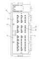
雄ハウジング11は、図1に示すように、前面に開口した横長の箱状に形成されており、前面開口部が、図示しない相手の雌ハウジングが嵌合される嵌合凹部12とされている。
雄端子15は、L型に曲げ形成されたタブによって構成されており、各雄端子15は、それぞれの前端15Aが、嵌合凹部12の奥壁13から複数段に亘り横方向に列をなして同嵌合凹部12に突出した形態で装着されており、各雄端子15の後端15B側は、奥壁13の背面側において、縦横に整列された形態で下向きに突出されている。
As shown in FIG. 1, the
The
後記するように、雄ハウジング11が回路基板1の端縁部の所定位置に取り付けられると、同雄ハウジング11に装着された各雄端子15の後端15Bが、回路基板1に整列して形成された対応するスルーホール(図示せず)に挿入されるようになっている。
As will be described later, when the
続いて、雄ハウジング11の回路基板1に対する取付構造を説明する。
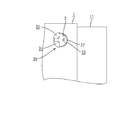
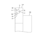
図2ないし図5に示すように、雄ハウジング11の背面における左右両端部の略中央高さに位置には、それぞれ取付板17が水平姿勢で形成されており、各取付板17の下面からは、回路基板1に形成された取付孔2に挿入される取付部20が、下向きに突設されている。回路基板1の取付孔2は円形孔からなり、上記したスルーホールの形成領域の両側に一対が形成されている。
Next, a structure for attaching the
As shown in FIGS. 2 to 5,
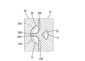
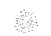
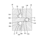
取付部20は、円盤状の基板21の周縁部に沿うようにして3本の挿入片が所定の角度間隔を開けて配されており、より詳細には、図6に示すように、上記の基板21の周縁部のうちの前縁位置に1本と、同位置から後方に135°(α)隔たった左右の斜め後方位置に1本ずつが形成されている。3本の挿入片のうち、前縁位置の挿入片が固定片23とされているとともに、残りの2本の挿入片が弾性係止片30とされている。
The
先に弾性係止片30を説明すると、弾性係止片30は、1/4円の基部にテーパ面を形成したような扇形断面をなし、その外面30Aが、取付孔2の内周面に倣った円弧面とされている。また、各弾性係止片30の互いに直交した平面状の側面30Bは、後記する型抜きの関係で、前後方向または左右方向を向いて形成されている。
上記の弾性係止片30の外面30Aの下端部には、断面略山形をなす係止部31が全幅に亘って膨出形成されている。この係止部31の上側の傾斜面が、回路基板1の取付孔2における裏側の孔縁に係止する係止面32となっているとともに、下側の傾斜面がガイド面33とされている。
The
At the lower end portion of the
一方の固定片23は、1/4円形断面をなし、外面24が、取付孔2の内周面に倣った円弧面とされている。この固定片23は、後記する型抜きの関係から、両側面が下端側に向けて次第に薄肉となるテーパ状に形成されており、特に同固定片23は、上記した両弾性係止片30よりも所定寸法長く形成されている。この固定片23の下端部の外面側には、傾斜面が削成されてガイド面25とされている。
また、固定片23の円弧形をなす外面24における中央幅位置には、略半円形断面をなす背の低いリブ27が全長に亘って形成されている。
One
Further, a
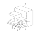
取付部20を構成する1本の固定片23と2本の弾性係止片30とが、上記した形状並びに配置とされたことにより、それらは成形型内において、図7のようにして成形される。
2本の弾性係止片30における係止部31を含む円弧形をなす外面30Aは、当該取付部20を含む雄ハウジング11を成形するべく前後の成形型のうち、後側の成形型40によって成形可能である。
また、上記の各弾性係止片30の両側面30Bと、リブ27を含む固定片23の全周面とは、上下方向に可動のスライド型41によって成形される。弾性係止片30並びに固定片23について、スライド型41に対するアンダーカット部分がないから、無理抜きされることはない。
Since the one fixing
The
Further, both side surfaces 30B of each
続いて、基板用コネクタ10を回路基板1に取り付ける手順の一例を説明する。
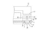
雄ハウジング11を回路基板1に取り付けるには、雄ハウジング11の背面の左右両端部に下向きに形成された一対の取付部20が、図3及び図4の矢線に示すように、回路基板1に形成された対応する取付孔2に挿入される。そのとき他の2本の弾性係止片30よりも長い固定片23の先端が、必要に応じてガイド面25で案内されながら、先に取付孔2内に挿入される。続いて2本の弾性係止片30が挿入されるが、係止部31の下面側のガイド面33が取付孔2の表側の孔縁に当たることで弾性係止片30が内方に撓み変位しつつ、係止部31の頂点が取付孔2の内周面に摺接して押し込まれる。
Next, an example of a procedure for attaching the
In order to attach the
このとき、固定片23のリブ27が取付孔2の内周面の前部位置に押し付けられた状態において、他の2本の弾性係止片30の各係止部31が、取付孔2の内周面の左右の斜め後方位置に弾性的に押し付けられた状態で押し込まれ、すなわち取付部20は、取付孔2の内周面に対して全方向に亘ってほぼ均等に押付力を作用させた状態で押し込まれることとなって、取付部20はがたつきなく真直姿勢で取付孔2内に挿入され、ひいては雄ハウジング11が傾くことなく正規姿勢で回路基板1上に向けて押し込まれる。
At this time, in a state where the
両弾性係止片30の係止部31の頂点が取付孔2の裏側の孔縁を過ぎたところで、図8ないし図10に示すように、両弾性係止片30が復元変位して係止部31の上面側の係止面32が取付孔2の裏側の孔縁に係止し、これにより雄ハウジング11が回路基板1上に抜け止めされて取り付けられる。この間に、雄ハウジング11に列設された雄端子15の下向きの後端15Bが、回路基板1に形成された対応するスルーホールに挿入される。その後に半田付けされることで、雄端子15の後端15Bが対応するスルーホール(導電部)に対して電気接続されつつ固定されることになる。
When the apex of the locking
本実施形態によれば、雄ハウジング11に一体的に形成した取付部20を回路基板1の取付孔2に押し込んで取り付ける構造であるから、ねじ止めする場合と比較すると、部品点数が削減され、取付作業も簡易化される。
また、固定片23が先に取付孔2に挿入されて位置決めされたのち、同固定片23が引き続き挿入状態にあるままに他の2本の弾性係止片30も揃って取付孔2に挿入されて押し込まれ、言い換えると固定片23が誘い込みの機能を果たして、固定片23並びに両弾性係止片30の全てを揃ってスムーズに取付孔2に押し込むことができる。
According to the present embodiment, since the mounting
Further, after the fixing
取付部20が取付孔2に押し込まれる間、固定片23並びに他の2本の弾性係止片30から、取付孔2の内周面に対して全方向に亘ってほぼ均等に押付力が作用し、これにより取付部20ががたつきなく真直姿勢で挿入され、もって雄ハウジング11が傾くことなく正規姿勢で回路基板1上に取り付けられる。それに伴い、雄ハウジング11に装着された雄端子15の後端15Bが、回路基板1の対応するスルーホールに正規姿勢で挿入され、引き続く半田付けにより、確実な電気的な接続と固定とを図ることができる。
なお、固定片23の外面にリブ27を設けて同リブ27を取付孔2の内周面に摺接させるようにしたから、挿入抵抗は小さく抑えられる。
While the mounting
Since the
本実施形態の取付部20を構成する固定片23と2本の弾性係止片30とは、前後方向に開閉する成形型のうち後側の成形型40と、上下方向に可動のスライド型41を用いて成形することができる。それにより、取付部20を雄ハウジング11の背面側に設定しながらも、雄ハウジング11に成形型(前側の成形型)の抜き用の開口を設けることなく取付部20を形成できる。
結果、取付部20を雄ハウジング11の側方に張り出して設ける必要がなく、また雄ハウジング11に対して抜き用の開口を設けるための余分な部分を設ける必要もないから、雄ハウジング11ひいては基板用コネクタ10の小型化を図ることに寄与し得る。
The fixed
As a result, it is not necessary to provide the mounting
<実施形態2>
次に、本発明の実施形態2を図12ないし図15によって説明する。
この実施形態では、雄ハウジング11Aに設ける取付部50の形成位置並びに取付部50自身の構造に変更が加えられている。
雄ハウジング11Aの背面における左右両端部の略中央高さに位置には、それぞれ取付板17Aが水平姿勢で形成され、特に各取付板17Aは雄ハウジング11Aの側面から外側に張り出して形成されており、各取付板17Aにおける雄ハウジング11Aの側面から張り出した部分における下面に、回路基板1に形成された取付孔2(図3参照)に挿入される取付部50が下向きに形成されている。なお、実施形態2における取付孔2の形成位置は、取付部50の形成位置と対応している。
<
Next, a second embodiment of the present invention will be described with reference to FIGS.
In this embodiment, changes are made to the formation position of the mounting
The mounting
取付部50の形状を説明する。ここで、実施形態1に示した取付部20で説明したのと同一機能を有する部位、部分については、必要に応じて同一符号を付して説明する。
取付部50は、円盤状の基板21の周縁部に、1本の固定片51と2本の弾性係止片55とが等角度間隔(120°)を開けて配され、より詳細には、図14に示すように、基板21の周縁部のうち前縁位置に固定片51が、左右の斜め後方位置にそれぞれ弾性係止片55が形成されている。
The shape of the
In the mounting
弾性係止片55は、環形の所定角度範囲を取り出したような断面をなし、その外面55Aが、取付孔2の内周面に倣った円弧面とされている。また、各弾性係止片55の互いに交差した平面状の両側面55Bにおける内側の角部にテーパ面55Cが形成され、特に両弾性係止片55における互いに対向したテーパ面55Cは、型抜きの関係で前後方向を向いた平行面となっている。
弾性係止片55の外面55Aの下端部には、実施形態1と同様に、断面略山形をなす係止部31が全幅に亘って膨出形成され、その上側の傾斜面が係止面32で、下側の傾斜面がガイド面33とされている。
The
At the lower end portion of the
固定片51は、断面形状について、環形の所定角度範囲を取り出したような形状で、外面51Aが取付孔2の内周面に倣った円弧面とされている。それ以外については、実施形態1の固定片23と同様に、両弾性係止片55よりも所定寸法長く形成されて、その下端部の外面側にガイド面25が形成されているとともに、円弧形をなす外面51Aにおける中央幅位置には、略半円形断面をなす背の低いリブ27が全長に亘って形成されている。
The fixed
取付部50を構成する1本の固定片51と2本の弾性係止片55とが、上記した形状並びに配置とされたことにより、それらは成形型内において、図15のようにして成形される。
端的には、当該取付部50を含む雄ハウジング11を成形するべく前後の成形型45,46のみで成形可能であり、より具体的には、両弾性係止片55における外面55A(係止部31を含む)と互いに対向した側の側面55B(テーパ面55Cを含む)、並びに固定片51における両側面51Bと内面51Cは、後側の成形型46によって成形され、また、両弾性係止片55における他方の側面55B(テーパ面55Cを含む)、並びに固定片51におけるリブ27を含む外面51Aは、前側の成形型45によって成形可能である。
Since one fixing
In short, the
実施形態2の基板用コネクタも、上記実施形態1と同様の手順によって回路基板1に取り付けることができ、同様の効果を得ることができる。
簡単に繰り返すと、雄ハウジング11Aに一体的に形成した取付部50を回路基板1の取付孔2に押し込んで取り付ける構造であるから、部品点数の削減と、取付作業の簡易化が図られる。また、固定片51が誘い込みの機能を果たして、取付部50全体をスムーズに取付孔2に押し込むことができる。
The board connector of the second embodiment can also be attached to the
If it repeats simply, since it is the structure where the
取付部50が取付孔2に押し込まれる間、固定片51並びに他の2本の弾性係止片55から、取付孔2の内周面に対して全方向に亘りほぼ均等に押付力が作用することで、取付部50ががたつきなく真直姿勢で挿入され、雄ハウジング11Aが傾くことなく正規姿勢で回路基板1上に取り付けられる。固定片51の外面に設けたリブ27を取付孔2の内面に摺接させるのであるから、挿入抵抗は小さく抑えられる。
実施形態2の取付部50は、スライド型を用いることなく前後方向に開閉する成形型45,46のみで成形可能である。
While the mounting
The mounting
<他の実施形態>
本発明は上記記述及び図面によって説明した実施形態に限定されるものではなく、例えば次のような実施形態も本発明の技術的範囲に含まれる。
(1)上記実施形態では、取付部を構成する挿入片が3本の場合を例示したが、挿入片は4本以上が略等角度間隔で配されて、そのうちの1本が固定片とされていればよい。
(2)固定片の外面にリブを設けることは割愛してもよく、そのようなものも本発明の技術的範囲に含まれる。
(3)上記実施形態では、雄ハウジングに装着された雄端子の後端を回路基板のスルーホールに固定する手段として半田付けする場合を例示したが、プレスフィット端子のようにスルーホール内に圧入して固定する形式の基板用コネクタについても、本発明は同様に適用することが可能である。
<Other embodiments>
The present invention is not limited to the embodiments described with reference to the above description and drawings. For example, the following embodiments are also included in the technical scope of the present invention.
(1) In the above embodiment, the case where there are three insertion pieces constituting the attachment portion is illustrated, but four or more insertion pieces are arranged at substantially equal angular intervals, and one of them is a fixed piece. It only has to be.
(2) Providing ribs on the outer surface of the fixed piece may be omitted, and such a thing is also included in the technical scope of the present invention.
(3) In the above embodiment, the case where the rear end of the male terminal attached to the male housing is soldered as a means for fixing to the through hole of the circuit board is illustrated. However, it is press-fitted into the through hole like a press-fit terminal. The present invention can also be applied to a board connector of a type that is fixed in the same manner.
1…回路基板
2…取付孔
10…基板用コネクタ
11,11A…雄ハウジング(コネクタハウジング)
15…雄端子(端子金具)
15B…(雄端子15の)後端
17,17A…取付板
20…取付部
21…基板
23…固定片
24…(固定片23の)外面
27…リブ
30…弾性係止片
31…係止部
50…取付部
51…固定片
51A…(固定片51の)外面
DESCRIPTION OF
15 ... Male terminal (terminal fitting)
15B: Rear end (of male terminal 15) 17, 17A ... Mounting
Claims (3)
前記コネクタハウジングの側面には、前記回路基板に形成された円形の取付孔に挿入される取付部が設けられ、
この取付部は、3以上の複数本の挿入片が略等角度間隔を開けて平面円形をなすように配されることで構成され、前記挿入片のうちの1本の挿入片が固定片とされている一方、残りの挿入片は、先端に前記取付孔の裏側の孔縁に係止する係止部を有して弾性変位可能な弾性係止片とされており、かつ前記固定片が前記弾性係止片よりも所定寸法長く形成されていることを特徴とする基板用コネクタの取付構造。 A connector for a board in which a plurality of terminal fittings are arranged in a connector housing is mounted on a circuit board, and a rear end of the terminal fitting is inserted and fixed in a through hole formed in the circuit board. A structure for attaching a housing to the circuit board,
A side surface of the connector housing is provided with a mounting portion to be inserted into a circular mounting hole formed in the circuit board,
The attachment portion is configured by arranging three or more insertion pieces so as to form a plane circle with substantially equal angular intervals, and one of the insertion pieces is a fixed piece. On the other hand, the remaining insertion piece is an elastic locking piece that has a locking portion that locks to the hole edge on the back side of the mounting hole at the tip, and is elastically displaceable. A board connector mounting structure characterized by being formed longer than the elastic locking piece by a predetermined dimension.
Priority Applications (1)
| Application Number | Priority Date | Filing Date | Title |
|---|---|---|---|
| JP2011128160A JP2012256477A (en) | 2011-06-08 | 2011-06-08 | Mounting structure of connector for substrate |
Applications Claiming Priority (1)
| Application Number | Priority Date | Filing Date | Title |
|---|---|---|---|
| JP2011128160A JP2012256477A (en) | 2011-06-08 | 2011-06-08 | Mounting structure of connector for substrate |
Publications (1)
| Publication Number | Publication Date |
|---|---|
| JP2012256477A true JP2012256477A (en) | 2012-12-27 |
Family
ID=47527873
Family Applications (1)
| Application Number | Title | Priority Date | Filing Date |
|---|---|---|---|
| JP2011128160A Pending JP2012256477A (en) | 2011-06-08 | 2011-06-08 | Mounting structure of connector for substrate |
Country Status (1)
| Country | Link |
|---|---|
| JP (1) | JP2012256477A (en) |
Cited By (5)
| Publication number | Priority date | Publication date | Assignee | Title |
|---|---|---|---|---|
| JP2015049957A (en) * | 2013-08-30 | 2015-03-16 | 住友電装株式会社 | Structure for mounting connector for substrate |
| JP5692333B1 (en) * | 2013-10-30 | 2015-04-01 | 第一精工株式会社 | Electrical connector housing |
| JP2015079714A (en) * | 2013-10-18 | 2015-04-23 | 住友電装株式会社 | Substrate connector |
| EP3579345A1 (en) * | 2018-06-05 | 2019-12-11 | Yazaki (China) Investment Corporation | Receptor connector |
| CN114122765A (en) * | 2020-08-25 | 2022-03-01 | 住友电装株式会社 | Connector with a locking member |
Citations (3)
| Publication number | Priority date | Publication date | Assignee | Title |
|---|---|---|---|---|
| US5613877A (en) * | 1995-11-02 | 1997-03-25 | Molex Incorporated | Electric connector boardlock |
| JP2002151186A (en) * | 2000-11-09 | 2002-05-24 | Taiko Denki Co Ltd | Connector |
| JP2008166180A (en) * | 2006-12-28 | 2008-07-17 | Keihin Corp | Connection structure of electronic circuit board and connector |
-
2011
- 2011-06-08 JP JP2011128160A patent/JP2012256477A/en active Pending
Patent Citations (3)
| Publication number | Priority date | Publication date | Assignee | Title |
|---|---|---|---|---|
| US5613877A (en) * | 1995-11-02 | 1997-03-25 | Molex Incorporated | Electric connector boardlock |
| JP2002151186A (en) * | 2000-11-09 | 2002-05-24 | Taiko Denki Co Ltd | Connector |
| JP2008166180A (en) * | 2006-12-28 | 2008-07-17 | Keihin Corp | Connection structure of electronic circuit board and connector |
Cited By (10)
| Publication number | Priority date | Publication date | Assignee | Title |
|---|---|---|---|---|
| JP2015049957A (en) * | 2013-08-30 | 2015-03-16 | 住友電装株式会社 | Structure for mounting connector for substrate |
| CN104425915A (en) * | 2013-08-30 | 2015-03-18 | 住友电装株式会社 | Mounting structure for board connector |
| US9209536B2 (en) | 2013-08-30 | 2015-12-08 | Sumitomo Wiring Systems, Ltd. | Mounting structure for board connector |
| JP2015079714A (en) * | 2013-10-18 | 2015-04-23 | 住友電装株式会社 | Substrate connector |
| JP5692333B1 (en) * | 2013-10-30 | 2015-04-01 | 第一精工株式会社 | Electrical connector housing |
| US9325088B2 (en) | 2013-10-30 | 2016-04-26 | Dai-Ichi Seiko Co., Ltd | Leg unit with projections with arcuate outer surfaces for engaging a fixing hole in a printed circuit board |
| EP3579345A1 (en) * | 2018-06-05 | 2019-12-11 | Yazaki (China) Investment Corporation | Receptor connector |
| CN114122765A (en) * | 2020-08-25 | 2022-03-01 | 住友电装株式会社 | Connector with a locking member |
| JP2022037548A (en) * | 2020-08-25 | 2022-03-09 | 住友電装株式会社 | connector |
| JP7428972B2 (en) | 2020-08-25 | 2024-02-07 | 住友電装株式会社 | connector |
Similar Documents
| Publication | Publication Date | Title |
|---|---|---|
| JP5881666B2 (en) | Manufacturing method of receptacle connector | |
| JP5901733B1 (en) | Cable connector | |
| JP3163750U (en) | Electrical connector | |
| US10263350B2 (en) | Electrical connector | |
| JP2008130244A (en) | Connector | |
| JP2012256477A (en) | Mounting structure of connector for substrate | |
| KR101425063B1 (en) | Connector | |
| JP2015220005A (en) | Board-to-board connector | |
| KR101514372B1 (en) | Connector | |
| JP5656117B2 (en) | Board connector | |
| JP4577061B2 (en) | Electrical junction box | |
| JP6057468B2 (en) | Waterproof connector | |
| JP2015049957A (en) | Structure for mounting connector for substrate | |
| JP5881891B2 (en) | Electronic component assembly structure and electrical junction box | |
| JP2012243676A (en) | Connector | |
| KR102239718B1 (en) | connection pin and connector and manufacturing method of connection pin | |
| JP2010123488A (en) | Double locking connector | |
| KR20170117693A (en) | Connector | |
| JP2013143286A (en) | Board connector | |
| US20130280942A1 (en) | Connector Housing | |
| JP5691803B2 (en) | Connector and electrical junction box | |
| JP2010092837A (en) | Connector | |
| JP6055939B2 (en) | Receptacle connector and method of manufacturing receptacle connector | |
| JP2020150600A (en) | Resin structure | |
| JP6093645B2 (en) | Joint connector |
Legal Events
| Date | Code | Title | Description |
|---|---|---|---|
| A621 | Written request for application examination |
Free format text: JAPANESE INTERMEDIATE CODE: A621 Effective date: 20131129 |
|
| A977 | Report on retrieval |
Free format text: JAPANESE INTERMEDIATE CODE: A971007 Effective date: 20140828 |
|
| A131 | Notification of reasons for refusal |
Free format text: JAPANESE INTERMEDIATE CODE: A131 Effective date: 20140902 |
|
| A521 | Written amendment |
Free format text: JAPANESE INTERMEDIATE CODE: A523 Effective date: 20141020 |
|
| A02 | Decision of refusal |
Free format text: JAPANESE INTERMEDIATE CODE: A02 Effective date: 20141118 |