JP2012255774A - High accuracy beam placement for local area navigation - Google Patents
High accuracy beam placement for local area navigation Download PDFInfo
- Publication number
- JP2012255774A JP2012255774A JP2012113991A JP2012113991A JP2012255774A JP 2012255774 A JP2012255774 A JP 2012255774A JP 2012113991 A JP2012113991 A JP 2012113991A JP 2012113991 A JP2012113991 A JP 2012113991A JP 2012255774 A JP2012255774 A JP 2012255774A
- Authority
- JP
- Japan
- Prior art keywords
- image
- fiducial
- feature
- interest
- array
- Prior art date
- Legal status (The legal status is an assumption and is not a legal conclusion. Google has not performed a legal analysis and makes no representation as to the accuracy of the status listed.)
- Granted
Links
- 238000000034 method Methods 0.000 claims abstract description 97
- 239000004065 semiconductor Substances 0.000 claims abstract description 23
- 239000002245 particle Substances 0.000 claims description 60
- 238000003384 imaging method Methods 0.000 claims description 26
- 238000010884 ion-beam technique Methods 0.000 claims description 23
- 238000003860 storage Methods 0.000 claims description 19
- 238000005530 etching Methods 0.000 claims description 10
- 238000000151 deposition Methods 0.000 claims description 9
- 230000008021 deposition Effects 0.000 claims description 9
- 238000001659 ion-beam spectroscopy Methods 0.000 claims description 4
- 238000010186 staining Methods 0.000 claims description 4
- 238000003909 pattern recognition Methods 0.000 abstract description 17
- 238000004519 manufacturing process Methods 0.000 abstract description 8
- 230000007547 defect Effects 0.000 abstract description 5
- 238000011960 computer-aided design Methods 0.000 description 44
- 230000008569 process Effects 0.000 description 33
- 238000012546 transfer Methods 0.000 description 33
- 238000010894 electron beam technology Methods 0.000 description 15
- 235000012431 wafers Nutrition 0.000 description 14
- 150000002500 ions Chemical class 0.000 description 12
- 238000012545 processing Methods 0.000 description 12
- 230000009977 dual effect Effects 0.000 description 10
- 238000010586 diagram Methods 0.000 description 8
- 230000015572 biosynthetic process Effects 0.000 description 6
- 230000009466 transformation Effects 0.000 description 6
- 239000000463 material Substances 0.000 description 5
- 239000000758 substrate Substances 0.000 description 5
- 238000004590 computer program Methods 0.000 description 4
- 238000003801 milling Methods 0.000 description 4
- 239000002344 surface layer Substances 0.000 description 4
- 238000004364 calculation method Methods 0.000 description 3
- 238000013461 design Methods 0.000 description 3
- 239000003550 marker Substances 0.000 description 3
- 238000005259 measurement Methods 0.000 description 3
- 239000000203 mixture Substances 0.000 description 3
- 238000012986 modification Methods 0.000 description 3
- 230000004048 modification Effects 0.000 description 3
- 230000003287 optical effect Effects 0.000 description 3
- 229920002120 photoresistant polymer Polymers 0.000 description 3
- 230000005855 radiation Effects 0.000 description 3
- 230000000007 visual effect Effects 0.000 description 3
- 238000004458 analytical method Methods 0.000 description 2
- 238000013459 approach Methods 0.000 description 2
- 230000007423 decrease Effects 0.000 description 2
- 230000000694 effects Effects 0.000 description 2
- 230000006870 function Effects 0.000 description 2
- 238000001459 lithography Methods 0.000 description 2
- 238000000059 patterning Methods 0.000 description 2
- 238000000206 photolithography Methods 0.000 description 2
- 238000005086 pumping Methods 0.000 description 2
- 230000002829 reductive effect Effects 0.000 description 2
- 238000000992 sputter etching Methods 0.000 description 2
- ZCYVEMRRCGMTRW-UHFFFAOYSA-N 7553-56-2 Chemical compound [I] ZCYVEMRRCGMTRW-UHFFFAOYSA-N 0.000 description 1
- 238000012935 Averaging Methods 0.000 description 1
- GYHNNYVSQQEPJS-UHFFFAOYSA-N Gallium Chemical compound [Ga] GYHNNYVSQQEPJS-UHFFFAOYSA-N 0.000 description 1
- 108010083687 Ion Pumps Proteins 0.000 description 1
- XUIMIQQOPSSXEZ-UHFFFAOYSA-N Silicon Chemical compound [Si] XUIMIQQOPSSXEZ-UHFFFAOYSA-N 0.000 description 1
- 230000001133 acceleration Effects 0.000 description 1
- 230000002411 adverse Effects 0.000 description 1
- 230000005540 biological transmission Effects 0.000 description 1
- 238000004891 communication Methods 0.000 description 1
- 238000010276 construction Methods 0.000 description 1
- 238000011161 development Methods 0.000 description 1
- 230000018109 developmental process Effects 0.000 description 1
- 238000009792 diffusion process Methods 0.000 description 1
- 238000006073 displacement reaction Methods 0.000 description 1
- 239000000428 dust Substances 0.000 description 1
- 238000003708 edge detection Methods 0.000 description 1
- 238000005516 engineering process Methods 0.000 description 1
- 238000002474 experimental method Methods 0.000 description 1
- 238000000605 extraction Methods 0.000 description 1
- 238000009432 framing Methods 0.000 description 1
- 229910052733 gallium Inorganic materials 0.000 description 1
- 238000002347 injection Methods 0.000 description 1
- 239000007924 injection Substances 0.000 description 1
- 238000007689 inspection Methods 0.000 description 1
- 229910052740 iodine Inorganic materials 0.000 description 1
- 239000011630 iodine Substances 0.000 description 1
- 239000010410 layer Substances 0.000 description 1
- 230000000670 limiting effect Effects 0.000 description 1
- 229910001338 liquidmetal Inorganic materials 0.000 description 1
- 238000013507 mapping Methods 0.000 description 1
- 229910052751 metal Inorganic materials 0.000 description 1
- 239000002184 metal Substances 0.000 description 1
- 229910021645 metal ion Inorganic materials 0.000 description 1
- 238000012544 monitoring process Methods 0.000 description 1
- 150000002902 organometallic compounds Chemical class 0.000 description 1
- 230000036961 partial effect Effects 0.000 description 1
- 239000002243 precursor Substances 0.000 description 1
- 238000004886 process control Methods 0.000 description 1
- 230000000979 retarding effect Effects 0.000 description 1
- 238000013515 script Methods 0.000 description 1
- 229910052710 silicon Inorganic materials 0.000 description 1
- 239000010703 silicon Substances 0.000 description 1
- 238000006467 substitution reaction Methods 0.000 description 1
- YLJREFDVOIBQDA-UHFFFAOYSA-N tacrine Chemical compound C1=CC=C2C(N)=C(CCCC3)C3=NC2=C1 YLJREFDVOIBQDA-UHFFFAOYSA-N 0.000 description 1
- 229960001685 tacrine Drugs 0.000 description 1
- 230000001131 transforming effect Effects 0.000 description 1
- 238000013519 translation Methods 0.000 description 1
Images


Classifications
-
- H—ELECTRICITY
- H01—ELECTRIC ELEMENTS
- H01L—SEMICONDUCTOR DEVICES NOT COVERED BY CLASS H10
- H01L22/00—Testing or measuring during manufacture or treatment; Reliability measurements, i.e. testing of parts without further processing to modify the parts as such; Structural arrangements therefor
- H01L22/10—Measuring as part of the manufacturing process
- H01L22/12—Measuring as part of the manufacturing process for structural parameters, e.g. thickness, line width, refractive index, temperature, warp, bond strength, defects, optical inspection, electrical measurement of structural dimensions, metallurgic measurement of diffusions
-
- G—PHYSICS
- G06—COMPUTING; CALCULATING OR COUNTING
- G06T—IMAGE DATA PROCESSING OR GENERATION, IN GENERAL
- G06T7/00—Image analysis
- G06T7/70—Determining position or orientation of objects or cameras
- G06T7/73—Determining position or orientation of objects or cameras using feature-based methods
-
- H—ELECTRICITY
- H01—ELECTRIC ELEMENTS
- H01J—ELECTRIC DISCHARGE TUBES OR DISCHARGE LAMPS
- H01J37/00—Discharge tubes with provision for introducing objects or material to be exposed to the discharge, e.g. for the purpose of examination or processing thereof
- H01J37/02—Details
- H01J37/22—Optical or photographic arrangements associated with the tube
- H01J37/222—Image processing arrangements associated with the tube
-
- H—ELECTRICITY
- H01—ELECTRIC ELEMENTS
- H01J—ELECTRIC DISCHARGE TUBES OR DISCHARGE LAMPS
- H01J37/00—Discharge tubes with provision for introducing objects or material to be exposed to the discharge, e.g. for the purpose of examination or processing thereof
- H01J37/26—Electron or ion microscopes; Electron or ion diffraction tubes
- H01J37/28—Electron or ion microscopes; Electron or ion diffraction tubes with scanning beams
-
- H—ELECTRICITY
- H01—ELECTRIC ELEMENTS
- H01J—ELECTRIC DISCHARGE TUBES OR DISCHARGE LAMPS
- H01J37/00—Discharge tubes with provision for introducing objects or material to be exposed to the discharge, e.g. for the purpose of examination or processing thereof
- H01J37/30—Electron-beam or ion-beam tubes for localised treatment of objects
- H01J37/304—Controlling tubes by information coming from the objects or from the beam, e.g. correction signals
- H01J37/3045—Object or beam position registration
-
- G—PHYSICS
- G06—COMPUTING; CALCULATING OR COUNTING
- G06T—IMAGE DATA PROCESSING OR GENERATION, IN GENERAL
- G06T2207/00—Indexing scheme for image analysis or image enhancement
- G06T2207/10—Image acquisition modality
- G06T2207/10056—Microscopic image
- G06T2207/10061—Microscopic image from scanning electron microscope
-
- G—PHYSICS
- G06—COMPUTING; CALCULATING OR COUNTING
- G06T—IMAGE DATA PROCESSING OR GENERATION, IN GENERAL
- G06T2207/00—Indexing scheme for image analysis or image enhancement
- G06T2207/30—Subject of image; Context of image processing
- G06T2207/30108—Industrial image inspection
- G06T2207/30148—Semiconductor; IC; Wafer
-
- H—ELECTRICITY
- H01—ELECTRIC ELEMENTS
- H01J—ELECTRIC DISCHARGE TUBES OR DISCHARGE LAMPS
- H01J2237/00—Discharge tubes exposing object to beam, e.g. for analysis treatment, etching, imaging
- H01J2237/30—Electron or ion beam tubes for processing objects
- H01J2237/317—Processing objects on a microscale
- H01J2237/31749—Focused ion beam
-
- H—ELECTRICITY
- H01—ELECTRIC ELEMENTS
- H01L—SEMICONDUCTOR DEVICES NOT COVERED BY CLASS H10
- H01L2924/00—Indexing scheme for arrangements or methods for connecting or disconnecting semiconductor or solid-state bodies as covered by H01L24/00
- H01L2924/0001—Technical content checked by a classifier
- H01L2924/0002—Not covered by any one of groups H01L24/00, H01L24/00 and H01L2224/00
Landscapes
- Engineering & Computer Science (AREA)
- Analytical Chemistry (AREA)
- Chemical & Material Sciences (AREA)
- Computer Vision & Pattern Recognition (AREA)
- Manufacturing & Machinery (AREA)
- Microelectronics & Electronic Packaging (AREA)
- Power Engineering (AREA)
- Computer Hardware Design (AREA)
- Physics & Mathematics (AREA)
- General Physics & Mathematics (AREA)
- Theoretical Computer Science (AREA)
- Testing Or Measuring Of Semiconductors Or The Like (AREA)
- Analysing Materials By The Use Of Radiation (AREA)
- Length-Measuring Devices Using Wave Or Particle Radiation (AREA)
- Design And Manufacture Of Integrated Circuits (AREA)
Abstract
Description
本発明は、粒子ビーム・システムにおけるステージ・ナビゲーション(stage navigation)およびビーム配置(beam placement)に関し、具体的には、FIB手段またはSEM手段による高解像度画像の取得を使用した試料表面の着目位置(site of interest)への高精度局所領域ナビゲーションに関する。 The present invention relates to stage navigation and beam placement in a particle beam system, and more particularly to a sample surface position of interest using high-resolution image acquisition by FIB or SEM means ( high accuracy local area navigation to site of interest).
集積回路の製造などの半導体製造は一般に、フォトリソグラフィの使用を伴う。通常はシリコン・ウェハである半導体基板に、回路を形成中に放射に露光すると溶解性が変化するフォトレジストなどの材料を塗布する。基板のどの領域を放射に露光するのかを制御するため、放射源と半導体基板の間に配置されたマスク、レチクルなどのリソグラフィ・ツールが影をつくる。露光後、露光した領域または露光していない領域からフォトレジストを除去し、ウェハの上に、後続のエッチング・プロセスまたは拡散プロセスの間、ウェハの一部分を保護するパターン形成されたフォトレジスト層を残す。 Semiconductor manufacturing, such as integrated circuit manufacturing, generally involves the use of photolithography. A semiconductor substrate, typically a silicon wafer, is coated with a material such as a photoresist whose solubility changes when exposed to radiation during circuit formation. In order to control which areas of the substrate are exposed to radiation, a lithography tool such as a mask, reticle, etc., placed between the radiation source and the semiconductor substrate casts a shadow. After exposure, the photoresist is removed from exposed or unexposed areas, leaving a patterned photoresist layer on the wafer that protects a portion of the wafer during subsequent etching or diffusion processes. .
このフォトリソグラフィ・プロセスによって、それぞれのウェハの上に、しばしば「チップ」と呼ばれる複数の集積回路デバイスまたはエレクトロメカニカル・デバイスを形成することができる。次いで、そのウェハを個々のダイに切断する。ダイはそれぞれ、単一の集積回路デバイスまたは単一のエレクトロメカニカル・デバイスを含む。最後に、これらのダイに更なる処理を行い、パッケージ化して、個々の集積回路チップまたは個々のエレクトロメカニカル・デバイスとする。 This photolithography process allows the formation of multiple integrated circuit devices or electromechanical devices, often referred to as “chips”, on each wafer. The wafer is then cut into individual dies. Each die includes a single integrated circuit device or a single electromechanical device. Finally, these dies are further processed and packaged into individual integrated circuit chips or individual electromechanical devices.
この製造プロセスの間、露光および集束は変動し、そのため、リソグラフィ・プロセスによって現像されたパターンを絶えず監視し、または測定して、パターンの寸法が許容範囲内にあるかどうかを判定する必要がある。しばしばプロセス制御と呼ばれるこのような監視の重要性は、パターン・サイズが小さくなるにつれて、特に最小フィーチャ(feature)サイズが、そのリソグラフィ・プロセスが使用可能な解像限界に近づくにつれて、相当に増大する。より高いデバイス密度を絶えず達成し続けるためには、ますます小さなフィーチャ・サイズが必要となる。このフィーチャ・サイズには、相互接続線の幅および間隔、コンタクト・ホールの間隔および直径、ならびにさまざまなフィーチャのコーナ(corner)、エッジ(edge)などの表面幾何構造が含まれることがある。 During this manufacturing process, exposure and focusing fluctuate, so the pattern developed by the lithographic process must be constantly monitored or measured to determine if the pattern dimensions are within acceptable limits. . The importance of such monitoring, often referred to as process control, increases considerably as the pattern size decreases, especially as the minimum feature size approaches the resolution limit at which the lithography process can be used. . In order to continue to achieve higher device density, ever smaller feature sizes are required. This feature size may include interconnect line widths and spacings, contact hole spacings and diameters, and surface geometries such as various feature corners, edges.
その結果、表面フィーチャを注意深く監視することがますます重要になっている。設計ルールが縮小するにつれて、処理の誤差に対する余裕も小さくなる。設計寸法からの小さなずれでさえも、完成した半導体デバイスの性能に悪影響を与える可能性がある。 As a result, it is becoming increasingly important to carefully monitor surface features. As the design rule shrinks, the margin for processing errors also decreases. Even small deviations from design dimensions can adversely affect the performance of the finished semiconductor device.
したがって、半導体業界の顧客は、メモリ・アレイ内の単一ビット不良、回路編集用の位置などのフィーチャの位置を特定するため、高精度ビーム配置を必要としている。ビーム・シフト・ナビゲーション・システムは、試料ドリフト(drift)、変位の非線形性などの欠点を有し、一般に視野に限界がある。粒子ビーム・システム上で使用される一般的な試料ステージの精度は±1〜2μmでしかない。(レーザ・エンコード・ステージ(laser encoded stage)のような)高精度ステージを使用せずに、100nm以下の精度でステージを対象の位置へ直接に駆動することはできない。レーザ・ステージは、100nmの精度を与える能力を有することがあるが、高価であり、レーザ・ステージは一般に傾けることができず、それによって機能を失うため、システムの柔軟性を限定する。さらに、一般的なレーザ・ステージの能力さえも超える約30nmの精度内で試料ステージを駆動することが望ましい。 Therefore, semiconductor industry customers require high precision beam placement to locate features such as single bit defects in a memory array, locations for circuit editing, and the like. Beam shift navigation systems have drawbacks such as sample drift, displacement nonlinearity, and generally have limited field of view. The accuracy of a typical sample stage used on a particle beam system is only ± 1 to 2 μm. Without using a high precision stage (such as a laser encoded stage), the stage cannot be driven directly to the target position with an accuracy of 100 nm or less. The laser stage may have the ability to give 100 nm accuracy, but is expensive and the laser stage is generally not tiltable, thereby losing functionality, thus limiting the flexibility of the system. In addition, it is desirable to drive the sample stage within an accuracy of about 30 nm that exceeds even the capabilities of typical laser stages.
一般的なメモリ・アレイでは、例えば個々のビット・セル(bit cell)内の欠陥を特徴づけまたは補正するために、アレイ内の単一のビット・セルへナビゲートすることがしばしば望ましい。一般的なビット・セルのサイズは50nm程度であり、アレイ全体の面積は100μm×100μmであることがある。個々のセルへのナビゲーションは現在、ステージをゆっくりと移動させ、所望の位置に到達するまでセルを手動で数えることによって、手動で実施されている。このような手動プロセスでは、特定のセルまで駆動するのに最長10分かかることがある。自動ナビゲーション、例えばパターン認識を使用してセルを自動的に数える自動ナビゲーションでは、セル・サイズまでのフィーチャ、この例では50nmまでのフィーチャを解像するのに十分な解像度でアレイを画像化する必要があるであろう。50nmのセルに対するパターン認識を確実に実行するのに十分な解像度を得るためには、少なくとも16K、ことによると64Kまたはそれ以上の解像度でアレイを画像化することが好ましいであろう。100μm×100μmのアレイのこのような高解像度走査(64K)(ドウェル時間(dwell time)は500nsとする)にはおよそ34分かかることになる。 In a typical memory array, it is often desirable to navigate to a single bit cell in the array, eg, to characterize or correct defects in individual bit cells. A typical bit cell size is on the order of 50 nm and the total array area may be 100 μm × 100 μm. Navigation to individual cells is currently performed manually by slowly moving the stage and manually counting the cells until the desired position is reached. Such manual processes can take up to 10 minutes to drive to a particular cell. Automatic navigation, for example automatic navigation that automatically counts cells using pattern recognition, requires the array to be imaged with sufficient resolution to resolve features up to cell size, in this example up to 50 nm. There will be. To obtain sufficient resolution to reliably perform pattern recognition for 50 nm cells, it may be preferable to image the array at a resolution of at least 16K, possibly 64K. Such a high resolution scan (64K) of a 100 μm × 100 μm array (dwell time is 500 ns) would take approximately 34 minutes.
したがって、半導体表面の局所領域内の対象の位置へ高精度でナビゲートする改良された方法であって、試料ステージの位置精度を超える精度でビームを配置することを可能にする改良された方法が依然として求められている。アレイ内の単一のビットへ、手動で数える必要なしに、素早く高精度にナビゲートするための改良された方法も求められている。さらに、このような改良された方法が、完全自動化または部分自動化に適していることも求められている。 Therefore, there is an improved method for navigating to a target location within a local region of a semiconductor surface with high accuracy, which makes it possible to place a beam with accuracy exceeding the location accuracy of the sample stage. There is still a need. There is also a need for an improved method for quickly and accurately navigating to a single bit in an array without the need for manual counting. Furthermore, there is a need for such an improved method to be suitable for full or partial automation.
したがって、本発明の目的は、特にFIB、SEMなどの粒子ビーム・システム内において、半導体表面の局所領域内の対象の位置へ高精度でナビゲートする改良された方法を提供することにある。 Accordingly, it is an object of the present invention to provide an improved method of navigating to a target location within a local region of a semiconductor surface with high accuracy, particularly in particle beam systems such as FIB, SEM.
本発明は、ターゲット位置に対する座標関係が既知である目に見える基準マークが局所領域内にあれば、画像化/パターン形成技法を使用して、局所領域(例えば一辺が200μmの領域)内の対象の位置へ高精度でナビゲートすることが可能な方法を示す。最初に、幅約4096画素のターゲット領域の高解像度画像を取得する。ターゲット領域の近くの2つ以上のアライメント・フィーチャの位置を特定する。画像上の対象の領域の上にCADポリゴンを重ねる。ディジタル・ズームを利用して、アライメント点の位置を精密に特定し、2点または3点CADポリゴン再位置合せを実行する。 The present invention uses imaging / patterning techniques to detect objects in a local region (eg, a region with a side of 200 μm) if a visible reference mark with a known coordinate relationship to the target location is in the local region. A method capable of navigating to a position with high accuracy is shown. First, a high-resolution image of a target area having a width of about 4096 pixels is acquired. Locate two or more alignment features near the target area. A CAD polygon is superimposed on a target area on the image. Use digital zoom to pinpoint the location of alignment points and perform 2-point or 3-point CAD polygon realignment.
画像と座標系とを正確に整列させた後、1つまたは複数の移転フィデューシャルを介して、そのアライメントを試料に移転することができる。試料上の着目フィーチャの近くの1つまたは複数の容易に識別可能なフィーチャを選択し、その移転フィデューシャル(1つまたは複数)と着目フィーチャの間のオフセットを記録する。次いで、座標系アライメントに基づいて、試料を、ずっと小さな視野で再画像化することができる。この第2の画像内で移転フィデューシャルを識別すれば、記録されたオフセットを使用して、着目フィーチャの位置を特定し、粒子ビームを正確に位置決めすることができる。 After the image and coordinate system are accurately aligned, the alignment can be transferred to the sample via one or more transfer fiducials. One or more easily identifiable features near the feature of interest on the sample are selected and the offset between the transfer fiducial (s) and the feature of interest is recorded. The sample can then be re-imaged with a much smaller field of view based on the coordinate system alignment. Once the transfer fiducial is identified in this second image, the recorded offset can be used to locate the feature of interest and accurately position the particle beam.
本発明の好ましい実施形態によれば、この大領域高解像度走査と、ディジタル・ズームと、理想化された座標系への画像の位置合せとの組合せによって、ステージの移動に依存せずに局所領域をナビゲートすることができる。一旦画像を取得してしまえば、試料ドリフトまたはビーム・ドリフトはアライメントに一切影響を及ぼさない。 According to a preferred embodiment of the present invention, this combination of large area high resolution scanning, digital zoom, and image alignment to an idealized coordinate system allows local regions to be independent of stage movement. Can be navigated. Once the image is acquired, sample drift or beam drift has no effect on alignment.
例えばメモリ・アレイまたは類似の構造内の個々のビット・セルの欠陥を特徴づけまたは補正するために、本発明の好ましい実施形態を使用して、メモリ・アレイまたは類似の構造内の単一のビット・セルへ迅速にナビゲートすることもできる。アレイ全体を走査するのではなく、その代わりにアレイの(X軸またはY軸に沿った)1つのエッジのセルの「ストリップ(strip)」だけを走査するために高解像度走査を使用して、所望のセルを含む列(row)の位置を特定し、続いて、位置が特定された列に沿って(もう一方の方向に)、所望のセル位置に到達するまで同様に高速走査する。これによって、アレイ全体を画像化するのにかかる大きな時間の消費なしに、パターン認識ツールを使用して、所望のセルへナビゲートするのに必要なセルを自動的に「数える」ことが可能になる。本発明の好ましい実施形態を使用すると一般に、5分未満で、単一のビット・セルの位置を自動的に特定することができ、それに比べて、先行技術のいくつかの方法では30分を超える時間がかかる。 For example, to characterize or correct individual bit cell defects in a memory array or similar structure, a preferred embodiment of the present invention can be used to generate a single bit in a memory array or similar structure. -You can navigate quickly to the cell. Instead of scanning the entire array, instead using a high resolution scan to scan only a "strip" of cells at one edge (along the X or Y axis) of the array, The position of the row containing the desired cell is identified, followed by a rapid scan in the same way along the identified column (in the other direction) until the desired cell position is reached. This allows the pattern recognition tool to automatically “count” the cells needed to navigate to the desired cell without consuming the significant time it takes to image the entire array. Become. Using preferred embodiments of the present invention, it is generally possible to automatically locate a single bit cell in less than 5 minutes, compared to more than 30 minutes in some prior art methods. take time.
以上では、以下の本発明の詳細な説明をより理解できるように、本発明の特徴および技術上の利点をかなり広く概説した。以下では、本発明の追加の特徴および利点を説明する。開示される着想および特定の実施形態を、本発明の同じ目的を達成する他の構造を変更しまたは設計するベースとして容易に利用することができることを当業者は理解すべきである。さらに、このような等価の構造は、添付の特許請求の範囲に記載された本発明の趣旨および範囲を逸脱しないことを当業者は理解すべきである。 The foregoing has outlined rather broadly the features and technical advantages of the present invention in order that the detailed description of the invention that follows may be better understood. The following describes additional features and advantages of the present invention. It should be appreciated by those skilled in the art that the disclosed concepts and specific embodiments can be readily utilized as a basis for modifying or designing other structures that achieve the same objectives of the present invention. Moreover, those skilled in the art should appreciate that such equivalent constructions do not depart from the spirit and scope of the invention as set forth in the appended claims.
次に、本発明および本発明の利点のより完全な理解のため、添付図面に関して書かれた以下の説明を参照する。 For a more complete understanding of the present invention and its advantages, reference is now made to the following description, taken in conjunction with the accompanying drawings.
これらの添付図面は、尺度が一律になることを意図して描かれたものではない。これらの添付図面では、さまざまな図に示された同一のまたはほぼ同一の構成要素がそれぞれ、同様の符号によって示されている。分かりやすくするため、全ての図面の全ての構成要素に符号が付けられてはいないことがある。 These accompanying drawings are not intended to be uniform in scale. In the accompanying drawings, each identical or nearly identical component that is illustrated in various figures is represented by a like numeral. For clarity, not all components in all drawings may be labeled.
本発明の好ましい実施形態は、半導体チップ製造分野の局所領域ナビゲーション用の高精度ビーム配置法を対象としている。本発明は、ステージ/ナビゲーション・システムが通常は高精度ナビゲーションを実施する能力を持たない場合であっても、比較的に大きな局所領域(例えば200μm×200μmの領域)内の対象の位置へ高精度でナビゲートすることが可能な方法を示す。 A preferred embodiment of the present invention is directed to a high precision beam placement method for local area navigation in the field of semiconductor chip manufacturing. The present invention provides high accuracy to target locations within a relatively large local area (eg, 200 μm × 200 μm area) even when the stage / navigation system does not normally have the ability to perform high precision navigation. Shows how you can navigate with.
本発明の好ましい実施形態によれば、最初に、比較的に大きなターゲット領域(着目フィーチャの位置および1つまたは複数の適当なアライメント・マークを含むより大きな領域)の高解像度画像を取得する。例えば、適当な高解像度領域は250μmの幅を有し、幅について約4096画素の解像度を有する。好ましい一実施形態によれば、対象の領域の上にCADポリゴンを重ね、2点または3点CADポリゴン再位置合せ(re−registration)を実行する。次いで、ディジタル・ズームを利用して、着目フィーチャを含む領域の位置を精密に特定する。追加のCAD位置合せプロセスを実行して、精度をより高めることができる。次いで、着目フィーチャの近くの1つまたは複数の適当な移転フィデューシャル(transfer fiducial)の位置を特定し、あるいは着目フィーチャの近くに1つまたは複数の適当な移転フィデューシャルを形成し、この大視野画像内のフィデューシャルと着目フィーチャの間のオフセット(offset)を記録する。次いで、検査/調査を実行するのに適したより小さな視野の画像を取得する。この画像内で移転フィデューシャルを識別し、オフセットを使用して、着目フィーチャの位置を正確に特定する。 According to a preferred embodiment of the present invention, first a high resolution image of a relatively large target area (a larger area containing the location of the feature of interest and one or more suitable alignment marks) is acquired. For example, a suitable high resolution area has a width of 250 μm and a resolution of about 4096 pixels for the width. According to a preferred embodiment, CAD polygons are overlaid on the region of interest and a two-point or three-point CAD polygon re-registration is performed. Next, using digital zoom, the position of the region including the feature of interest is precisely specified. Additional CAD registration processes can be performed to further improve accuracy. Then, locate one or more suitable transfer fiducials near the feature of interest, or form one or more suitable transfer fiducials near the feature of interest, Record the offset between the fiducial in the large field image and the feature of interest. A smaller field of view image suitable for performing the inspection / survey is then acquired. The transfer fiducial is identified in this image and the offset is used to accurately locate the feature of interest.
この大領域高解像度走査と、ディジタル・ズームと、理想化された座標系への画像の位置合せとの組合せによって、ステージの移動に依存せずに局所領域をナビゲートすることができる。一旦画像を取得してしまえば、試料ドリフトまたはビーム・ドリフトはアライメントに一切影響を及ぼさない。したがって、好ましい実施形態は、高精度ステージ/ナビゲーション・システムなしで、100nm未満の精度で試料上の位置へ正確にナビゲートすることを可能にし、いくつかの好ましい実施形態は、30nm以内のナビゲーションを可能にする。言い換えると、本発明の好ましい実施形態によれば、試料ステージは、±500nm以上の位置決め精度または位置決め誤差を有することがあるが、±100nmまたはそれよりも良い(すなわち100nm以下の)位置決め精度で着目フィーチャの位置を特定し、試料に対して粒子ビームを位置決めすることができる。より好ましくは、±30nmまたはそれよりも良い精度で、着目フィーチャの位置を特定すること(すなわち、粒子ビーム・システムが、試料上の着目フィーチャの位置へナビゲートすること)ができる。試料ステージが、±100nm以上の位置決め精度または誤差を有する場合であっても、本発明の好ましい実施形態では、±300nmまたはそれよりも良い位置決め精度で、着目フィーチャの位置を特定し、試料に対して粒子ビームを位置決めすることができる。 The combination of this large area high resolution scan, digital zoom, and image alignment to the idealized coordinate system allows the local area to be navigated independent of stage movement. Once the image is acquired, sample drift or beam drift has no effect on alignment. Accordingly, preferred embodiments allow for precise navigation to a location on the sample with sub-100 nm accuracy without a high precision stage / navigation system, and some preferred embodiments provide navigation within 30 nm. enable. In other words, according to a preferred embodiment of the present invention, the sample stage may have positioning accuracy or positioning error of ± 500 nm or more, but focus on positioning accuracy of ± 100 nm or better (ie, 100 nm or less). The location of the feature can be identified and the particle beam can be positioned with respect to the sample. More preferably, the location of the feature of interest can be identified (ie, the particle beam system navigates to the location of the feature of interest on the sample) with an accuracy of ± 30 nm or better. Even if the sample stage has a positioning accuracy or error of ± 100 nm or more, in a preferred embodiment of the present invention, the position of the feature of interest is specified with a positioning accuracy of ± 300 nm or better, and the sample stage is To position the particle beam.
本発明の好ましい方法または装置は多くの新規の態様を有し、本発明は、目的の異なるさまざまな方法または装置として具体化することができるため、全ての実施形態に全ての態様が含まれる必要はない。また、記載された実施形態の多くの態様は、別々に特許を受けることができる。 The preferred method or apparatus of the present invention has many novel aspects, and since the present invention can be embodied as various methods or apparatuses having different purposes, all embodiments need to include all aspects. There is no. In addition, many aspects of the described embodiments can be patented separately.
図1は、本発明の好ましい一実施形態に基づく局所領域ナビゲーション用の高精度ビーム配置の諸ステップを示す流れ図を示す。ステップ10で、(図12に示した後述するFIB/SEMなどの)一般的な先行技術の荷電粒子ビーム・システムに試料を、システム・ステージ上に試料を装着することによって装填する。本発明の好ましい一実施形態に基づく荷電粒子ビーム・システムは、集束イオン・ビーム・システム、電子ビーム・システムまたはデュアル・ビームFIB/SEMシステムとすることができる。試料は手動で装填し、または例えば自動ハンドラ・システムによって自動的に装填することができる。
FIG. 1 shows a flow diagram illustrating the steps of high precision beam placement for local area navigation according to a preferred embodiment of the present invention. At
本発明の好ましい実施形態は、レーザ・ステージなどの高精度ステージの使用を必要としない。分析または処理のために試料または加工物を荷電粒子ビーム・システムに装填するときに、着目フィーチャの精密な位置までステージを駆動するのは非常に難しい操作である。一般的な試料ステージの精度は約1〜2μmである。言い換えると、このような一般的なステージを特定の座標まで移動させたとき、位置の誤差は最大で±1〜2μmになりうる。(この方式で表現するときには、数値が大きいほど精度の低いステージであることを意味する。)100nm以下の精度でナビゲートすることができるレーザ干渉計ステージ(laser interferometer stage)(以後「レーザ・ステージ」)などの先進の高精度ステージは、非常に高価である。また、レーザ・ステージには、傾けることが一般にできない、現在使用されている大部分の荷電粒子ビーム・システムで使用することができないといったいくつかの重大な欠点がある。本発明は、高精度レーザ・ステージを必要とせずに100nm未満の精度でナビゲートする方法を提供する。好ましくは、本発明の実施形態は、精度(位置誤差)±500nmの試料ステージを使用した100nm未満ナビゲーション法またはビーム配置法を提供する。より好ましくは、本発明の実施形態は、精度(位置誤差)±1〜2μm以上の試料ステージを使用した100nm未満ナビゲーション法またはビーム配置法を提供する。 Preferred embodiments of the present invention do not require the use of a high precision stage such as a laser stage. When loading a sample or workpiece into a charged particle beam system for analysis or processing, driving the stage to a precise location of the feature of interest is a very difficult operation. The accuracy of a general sample stage is about 1 to 2 μm. In other words, when such a general stage is moved to a specific coordinate, the position error can be ± 1 to 2 μm at the maximum. (When expressed in this manner, a larger value means a lower precision stage.) A laser interferometer stage (hereinafter referred to as “laser stage”) that can be navigated with an accuracy of 100 nm or less. Advanced precision stages such as “)” are very expensive. Laser stages also have several significant drawbacks, such as being generally not tiltable and not available for most charged particle beam systems currently in use. The present invention provides a method for navigating with sub-100 nm accuracy without the need for a high-precision laser stage. Preferably, embodiments of the present invention provide a sub-100 nm navigation method or beam placement method using a sample stage with accuracy (positional error) ± 500 nm. More preferably, embodiments of the present invention provide a sub-100 nm navigation method or beam placement method using a sample stage with an accuracy (position error) of ± 1 to 2 μm or more.
試料を装填した後、ステップ12で、知られている方法を使用して、例えばダイのコーナでの一般的な3点ロックによって、試料のアライメントを実施する。このアライメントは、手動で、例えばオペレータが光学顕微鏡を使用することによって、または自動的に、例えば適正な向きを決定するために試料のノッチまたはフラット・エッジの位置を特定する自動ハンドラ・ロボットを使用することによって、実施することができる。
After loading the sample, the alignment of the sample is performed at
ステップ14で、着目フィーチャが、荷電粒子ビームによって走査されるターゲット領域(視野)内に位置するように、ステージを位置決めする。(例えば着目フィーチャが埋め込まれているときなど、場合によっては、画像内で着目フィーチャを実際に見ることができないこともある。)この位置決めは、位置座標またはCAD(computer−aided design)データを記憶し、それらを使用することによって実施することができる。視野は、使用するステージ/システムの精度を考慮して、着目フィーチャが、好ましくは画像と試料表面のフィーチャの位置を表す座標系との位置合せで使用するのに適した1つまたは複数の適当なアライメント・フィーチャ(後により詳細に論じる)とともに、画像化される領域内に位置することが保証されるように、十分に大きくとるべきである。より好ましくは、視野が、アライメント・フィーチャとして使用するのに適した少なくとも3つのフィーチャを含む。適当なフィーチャは、試料画像内および座標系オーバレイ(overlay)内において容易に認識できなければならない。
In
ステップ16で、荷電粒子ビームを用いて試料を高解像度で画像化する。画素サイズが必要な配置精度に匹敵するように、この画像は、十分な(十分に高い)解像度を有していなければならない。画像解像度は、画素サイズが、アライメント・マークを識別し、アライメント・マークの位置を高い精度で決定することを可能にする、十分に高いものであることが好ましい。解像度は、画素サイズが、アライメント・フィーチャのサイズに等しいか、またはアライメント・フィーチャのサイズよりも小さくなる、十分に高いものであることがより好ましい。例えば、本発明の好ましい一実施形態では、これが、幅250μmの画像に対して4096画素(またはそれ以上)の解像度を使用することができることを意味し、その場合、画素サイズは約50〜60nmになる。その結果、50〜60nmよりも大きなアライメント・フィーチャを容易に識別することができる。本発明の他の好ましい実施形態は、画素サイズが10〜100nm、より好ましくは30〜60nmになる画像解像度を使用する。
In
好ましいいくつかの実施形態では、着目フィーチャのサイズよりも大きな画素サイズを与える解像度を使用することもできるが、このより大きな画素サイズは位置誤差の一因となると考えられる。例えば、上の段落で説明した実施形態の画素サイズ(50〜60nm)を、サイズが30nmのアライメント・フィーチャとともに使用した場合、そのアライメント・フィーチャが画素内のどこに位置するのかを決定する術はない。その結果、(画素サイズだけに起因する)アライメント・フィーチャの位置誤差は、20〜30nm(50〜60nm−30nm)にもなりうる。この精度は、一般的なレーザ・ステージによって達成できる精度よりも依然として高いため、多くの場合、この精度は許容される。 In some preferred embodiments, a resolution that provides a larger pixel size than the size of the feature of interest can be used, but this larger pixel size is believed to contribute to position errors. For example, if the pixel size (50-60 nm) of the embodiment described in the above paragraph is used with an alignment feature with a size of 30 nm, there is no way to determine where the alignment feature is located within the pixel. . As a result, alignment feature position errors (due to pixel size alone) can be 20-30 nm (50-60 nm-30 nm). This accuracy is often acceptable because this accuracy is still higher than can be achieved with a typical laser stage.
ターゲット(着目フィーチャ)の位置および好ましくはアライメント・フィーチャの位置も、ある形の座標系において既知であるべきである。好ましい実施形態では、これらの位置を、CADオーバレイ(後により詳細に説明する)またはxy座標、または繰り返し配列の構造から決定することができる。 The location of the target (feature of interest) and preferably the location of the alignment feature should also be known in some form of coordinate system. In preferred embodiments, these positions can be determined from CAD overlay (described in more detail below) or xy coordinates, or the structure of a repeating sequence.
この画像の解像度は、画素サイズが少なくとも必要な精度に匹敵する十分なものであるべきである。例えば、好ましい一実施形態では、幅250μmの画像の幅が画素約4096個分であり、その場合、画素サイズは約60ナノメートルになる。この解像度は、サイズが60ナノメートル以上あるアライメント点などのフィーチャを画像化し、処理するのに適当であろう。しかしながら、60nmよりも小さなフィーチャに対しては、より高い解像度(およびその結果としてのより小さな画素サイズ)が必要となるであろう。 The resolution of this image should be sufficient that the pixel size is at least comparable to the required accuracy. For example, in a preferred embodiment, a 250 μm wide image is about 4096 pixels wide, in which case the pixel size is about 60 nanometers. This resolution may be appropriate for imaging and processing features such as alignment points that are 60 nanometers or larger in size. However, for features smaller than 60 nm, a higher resolution (and resulting smaller pixel size) will be required.
視野(水平フィールド幅(horizontal field width)またはHFWとも呼ばれる)画像解像度と画素間隔の間には正のバランス(direct balance)がある:HFW=(画素間隔)×(画素数)。250μm×250μmよりもはるかに大きな領域にわたってナビゲートするため、ここに示したものでは、パターン形成エンジンの解像度を幅8kまたは16kの画像に増大させない限り、より大きな画素間隔および起こりうる走査歪みによって得られる精度が低減しそうな結果になるであろう。場合によっては、走査歪み/非線形性を理解するためにマッピングが必要となることがある。 There is a positive balance between field of view (also called horizontal field width or HFW) image resolution and pixel spacing: HFW = (pixel spacing) × (number of pixels). In order to navigate over a much larger area than 250 μm × 250 μm, the one shown here can be obtained by larger pixel spacing and possible scanning distortions unless the resolution of the patterning engine is increased to 8k or 16k wide images. The resulting accuracy will likely be reduced. In some cases, mapping may be required to understand scan distortion / non-linearity.
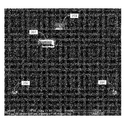
図2は、着目フィーチャの座標および最初の画像/CADオーバレイ位置合せ(後述)で使用する3つのアライメント・フィーチャの座標までステージを駆動することにより、前述のようにして得た試料の画像を示す。図2に示すように、(着目フィーチャを含む)ターゲット201および3つのアライメント・フィーチャ(202、203、204)は全て、表面層を貫通するミリング(milling)によって半導体表面に部分的に露出させたビア・フィールド(via field)である。視野は、使用するステージ/システムの精度を考慮して、着目フィーチャが、画像化される領域内に位置することが保証されるように、十分に大きくとるべきである。例えば、精度±2μmの試料ステージを備えた粒子ビーム・システムでは、着目フィーチャおよび約2000nm離れた3つのアライメント・フィーチャに対する視野は、着目フィーチャが画像化される視野内に位置することを保証するために少なくとも8μm×8μmであるべきである。しかしながら、本発明によれば、一般に、はるかに大きな約125μm×125μmの視野を使用することができる。 FIG. 2 shows an image of the sample obtained as described above by driving the stage to the coordinates of the feature of interest and the coordinates of the three alignment features used in the initial image / CAD overlay registration (described below). . As shown in FIG. 2, the target 201 (including the feature of interest) and all three alignment features (202, 203, 204) were all partially exposed to the semiconductor surface by milling through the surface layer. It is a via field. The field of view should be large enough to take into account the accuracy of the stage / system used and to ensure that the feature of interest is located within the area to be imaged. For example, in a particle beam system with an accuracy of ± 2 μm sample stage, the field of view for the feature of interest and three alignment features about 2000 nm apart is to ensure that the feature of interest is within the field of view to be imaged. Should be at least 8 μm × 8 μm. However, in accordance with the present invention, a much larger field of view of about 125 μm × 125 μm can generally be used.
再び図1を参照する。ステップ17で、CADポリゴン330(試料または加工物上のフィーチャの位置を表す理想化された幾何学的形状)を示すオーバレイを、半導体試料上の要素/フィーチャに対するCAD(computer−aided design)データから構築し、試料の荷電粒子ビーム画像の上に重ねることができる。このような座標系オーバレイを図3に示す。必要ならば、後述するように、CADオーバレイと画像の間の最初の位置合せを実行することができる。図3では、CADポリゴンによって指示されたいくつかの半導体フィーチャが露出しておらず、依然として表面層の下に埋め込まれていることに留意されたい。
Refer to FIG. 1 again. In
一般に、図3および4に示すように、画像に対するオーバレイの最初の位置決めは、おそらくいくぶんかは不正確である。任意選択のステップ18で、ディジタル拡大を使用して、ターゲットおよびアライメント点にズームイン(zoom in)することができる。一旦ターゲット領域を走査してしまえば、ユーザは、ディジタル・ズームを使用して、フィデューシャルまたは着目フィーチャの位置を特定するために、走査した画像を「ナビゲート」することができる。画像をナビゲートするのは、ステージを移動させ、試料を再画像化することによってナビゲートするよりもはるかに速く、容易である。ディジタル・ズーム(例えば図4の8:1程度のズーム)によって、ユーザは、着目フィーチャを含むおおまかな領域の位置を迅速に特定し、次いで、ズームインして、着目フィーチャ、座標オーバレイとともに使用するアライメント・フィーチャ、および/または後述する移転フィデューシャルの位置をより正確に特定することができる。図4では、拡大された画像によって、ビア340とCADポリゴン330とが正確には整列(align)していないことが明らかである。
In general, as shown in FIGS. 3 and 4, the initial positioning of the overlay relative to the image is probably somewhat inaccurate. In
本発明の好ましい実施形態では、画像とオーバレイの間の座標系位置合せを実行して、画像とCADオーバレイとをより正確に整列させるため、オペレータが、ディジタル・ズームを使用して、画像(およびCADオーバレイ)上の着目フィーチャまたは着目フィーチャの付近にズームインすることができる。当業者なら理解するとおり、ディジタル・ズームの使用は、例えばコンピュータ・モニタ上で人間のオペレータに対して視覚的に表示することができる詳細さのレベルの固有の限界を克服するのに役立つ。しかしながら、本発明の好ましいいくつかの実施形態では、例えば画像認識/マシン・ビジョン(machine vision)のような画像データのコンピュータ解析法を使用することによって、人間オペレータの代わりに、自動コンピュータ制御を使用することができる。自動実施形態に対してディジタル・ズームを使用する必要はないことは明白であろう。 In a preferred embodiment of the present invention, the operator uses digital zoom to perform an image (and a coordinate system alignment between the image and the overlay to more accurately align the image and the CAD overlay. The target feature on the CAD overlay) or the vicinity of the target feature can be zoomed in. As will be appreciated by those skilled in the art, the use of digital zoom helps overcome the inherent limitations in the level of detail that can be visually displayed to a human operator, eg, on a computer monitor. However, in some preferred embodiments of the present invention, automatic computer control is used instead of human operators by using computer analysis methods of image data such as image recognition / machine vision. can do. It will be clear that it is not necessary to use digital zoom for the automatic embodiment.
次いで、例えばマウス、画面上のカーソルなどのコンピュータ・ポインティング・デバイスを使用することによって、アライメント点および座標系オーバレイ上の対応する要素を識別することができる。図5は、この再位置合せプロセスの最初のステップを示す。ユーザは、ディジタル拡大を使用して、画像およびCADオーバレイにズームインし、画像内のさまざまな領域に対する局所的なオフセットを指定することができる。ディジタル拡大されている領域は、サムネイル・ビュー551内に正方形550として示される。図5に示すように、この画像は、アライメント点202のところにディジタル・ズームされている。再び図1を参照する。ステップ20で、オペレータは、図5に示すように、1つのCADポリゴン330の中心544を(マウスまたは他の適当なポインティング・デバイスで)クリックし、次いで試料画像内の対応するフィーチャ(ビア340)の中心542をクリックすることができる。次いで、このプロセスを、図6に示すようにアライメント・フィーチャ204に対して繰り返し(ステップ22)、図7に示すようにアライメント・フィーチャ203のところで繰り返す(ステップ24)ことができる。
The alignment points and corresponding elements on the coordinate system overlay can then be identified by using a computer pointing device such as a mouse, a cursor on the screen, for example. FIG. 5 shows the first step of this realignment process. The user can use digital magnification to zoom in on the image and CAD overlay and specify local offsets for various regions within the image. The digitally magnified area is shown as a square 550 in the
アライメント・フィーチャの位置および座標系オーバレイ内の対応する要素の位置を識別した後、ステップ26で、画像上の複数のアライメント点とCADオーバレイとの間のターゲット領域内におけるオフセットまたは重ね合せ誤差を測定することができる。図4の誤差は、ターゲット領域内で約1.4μmである。この誤差を補正するため、ステップ28で3点再位置合せを実行し、CADオーバレイを引き伸ばし、回転させ、かつ/または移動させて、画像と整合させる。
After identifying the position of the alignment feature and the position of the corresponding element in the coordinate system overlay, step 26 measures the offset or registration error in the target area between the alignment points on the image and the CAD overlay. can do. The error of FIG. 4 is about 1.4 μm in the target area. To correct this error, a three-point realignment is performed at
当業者なら理解するとおり、CADオーバレイと画像の間のオフセット誤差は、最初のステージ・ロックにおけるオペレータの誤り、FIB画像の不精密な較正(拡大および/または回転)、局所的なダイの歪み、またはイオン・カラム偏向システムの非線形性など、多くの原因から生じうる。誤差の原因が何であれ、CADオーバレイと大視野FIB画像内の全ての点との間の完全な一致を達成することは通常不可能である。この問題を解決する1つの方法は、CADオーバレイを必要に応じて引き伸ばし、移動させ、かつ/または回転させる3点再位置合せを実行して、状況に応じた特定のFIB画像の整合を達成することである。このタイプの画像位置合せは、本発明の譲受人でもあるFEI Company社(米オレゴン州Hillsboro)に譲渡された、参照によって本明細書に組み込まれているLindquist他の「Image−to−Image Registration Focused Ion Beam System」という名称の米国特許第5,541,411号において詳細に論じられている。 As will be appreciated by those skilled in the art, the offset error between the CAD overlay and the image can be an operator error in the initial stage lock, inaccurate calibration of the FIB image (magnification and / or rotation), local die distortion, Or it can come from many sources, such as non-linearity of the ion column deflection system. Whatever the cause of the error, it is usually impossible to achieve a perfect match between the CAD overlay and all points in the large field FIB image. One way to solve this problem is to perform a three-point realignment that stretches, moves, and / or rotates the CAD overlay as needed to achieve a specific FIB image alignment in context. That is. This type of image registration is described in Lindquist et al., “Image-to-Image Registration Focused,” incorporated herein by reference, assigned to FEI Company (Hillsboro, Oreg.), The assignee of the present invention. This is discussed in detail in US Pat. No. 5,541,411 entitled “Ion Beam System”.
Lindquistによって記述され、図5〜8によって示されているように、この位置合せ操作は、例えば粒子ビーム画像上の3点、および(本発明の好ましい実施形態によればCADオーバレイなどの)整列させるもう一方の画像上の対応する3点を選択することを含む。これらのアライメント点は、マウスを、ディスプレイからの視覚フィードバックとともに使用することによって対話方式で選択することができる。例えば、粒子ビーム画像内の視認可能なアライメント点としてアライメント点R1、R2およびR3を選択した場合には、位置合せを実行したい座標系オーバレイの対応する3点(C1、C2、C3)を選択する。画像内および座標系内の対応する点を選択した後、プロセスは、基準画像の点(R1、R2、R3)と前の画像(prior image)上の点(C1、C2、C3)との間で、T(C1)=R1、T(C2)=R2およびT(C3)=R3となるような変換Tを決定する。画面の特定の座標系内のこれらの点の座標位置は既知であるため、点間の変換は、線形代数法によって容易に決定される。 As described by Lindquist and illustrated by FIGS. 5-8, this alignment operation aligns, for example, three points on the particle beam image, and (such as a CAD overlay according to a preferred embodiment of the present invention) Including selecting the corresponding three points on the other image. These alignment points can be selected interactively by using the mouse with visual feedback from the display. For example, when alignment points R1, R2, and R3 are selected as visible alignment points in the particle beam image, three corresponding points (C1, C2, C3) of the coordinate system overlay to be aligned are selected. . After selecting the corresponding point in the image and the coordinate system, the process is between the point (R1, R2, R3) of the reference image and the point (C1, C2, C3) on the previous image (prior image). The transformation T is determined such that T (C1) = R1, T (C2) = R2, and T (C3) = R3. Since the coordinate position of these points within a particular coordinate system of the screen is known, the transformation between points is easily determined by linear algebra.
変換演算Tを決定した後、新たな空の(empty)(すなわちブランク(blank))画像を作成し、次いでループに入り、この新たな画像内の第1の画素を選択する。画素を選択した後、全ての画素を処理したかどうかについての判定を実施する。全ての画素を処理した場合、位置合せは完了であり、このプロセスを出る。しかしながら、処理していない画素がある場合には、座標変換Tを使用してプロセスを継続し、前の画像から対応する画素を選択する。次いで、前の画像から選択した画素データを、前の画像から、新たな画像の選択された画素位置へ読み込む。変換が、新たな画像の選択された位置を、前の画像の境界の外側にマップしている場合には、その新たな画像位置に空白データ(null data)を配置する。この空白データは例えばブランク表現または黒の背景表現を含むことができる。次に、プロセスをループバックして、再び新たな画像内の次の画素を選択し、新たな画像内の全ての画素が処理されるときまでプロセスを繰り返し継続する。 After determining the transformation operation T, a new empty (ie, blank) image is created and then a loop is entered to select the first pixel in the new image. After selecting a pixel, a determination is made as to whether all pixels have been processed. If all pixels have been processed, the alignment is complete and the process is exited. However, if there are unprocessed pixels, the process continues using the coordinate transformation T to select the corresponding pixels from the previous image. Next, the pixel data selected from the previous image is read from the previous image into the selected pixel position of the new image. If the transformation maps the selected position of the new image outside the boundary of the previous image, blank data (null data) is placed at the new image position. This blank data can include, for example, a blank representation or a black background representation. The process is then looped back to select the next pixel in the new image again and continue the process repeatedly until all the pixels in the new image are processed.
好ましい一実施形態では、オフセットの計算および画像とCADポリゴンの位置合せが、自動化されたコンピュータ・スクリプトを介して実行される。位置合せが完了した後、オーバレイとターゲット・ビアは、図8に示すように正確に整列している。 In a preferred embodiment, offset calculation and image and CAD polygon alignment are performed via automated computer scripts. After alignment is complete, the overlay and target via are correctly aligned as shown in FIG.
この変換演算は、画像間の平行移動、回転、尺度および傾斜角の差を調整するため、新たな画像は、最初の画像に比べて多少歪んでいることがある。上記のステップによれば、画像−画像位置合せは、荷電粒子画像内および座標系内の対応する3つのアライメント点を選択することによって実施することが好ましいが、これとは異なる数のアライメント点を使用することができ、点の数が多いほどアライメントの精度は高まる。対応するアライメント点間の変換を決定し、位置合せを実施する画像に適用して、適切に位置合せされた出力画像を生成する。代替として、精度を向上させる任意選択のステップは、ターゲット位置に近い、別のアライメント・フィーチャを含む追加の位置を画像化するステップである。次いで、これらの別個の画像によって指示された位置を平均することによって、ターゲット位置を決定する。このステップは特に、1画像につき1つのアライメント・フィーチャを使用するときに良好な精度を提供するために望ましい。これらのステップは、コンピュータ・プロセッサによって適切に実行されることが好ましく、これらのさまざまな画像は、画像バッファに記憶され、適当なディスプレイ上に表示されたビット・マップ画像(bit mapped image)である。 This transformation operation adjusts the translation, rotation, scale, and tilt angle differences between the images, so the new image may be somewhat distorted compared to the original image. According to the above steps, image-image registration is preferably performed by selecting three corresponding alignment points in the charged particle image and in the coordinate system, but a different number of alignment points is used. The higher the number of points, the higher the alignment accuracy. Transforms between corresponding alignment points are determined and applied to the image to be aligned to produce a properly aligned output image. Alternatively, an optional step to improve accuracy is to image an additional location that includes another alignment feature that is close to the target location. The target position is then determined by averaging the positions indicated by these separate images. This step is particularly desirable to provide good accuracy when using one alignment feature per image. These steps are preferably performed suitably by a computer processor, and these various images are bit mapped images stored in an image buffer and displayed on a suitable display. .
画像と座標系とを正確に整列させた後、そのアライメントを試料に「移転する(transfer)」必要がある。本発明の好ましい実施形態によれば、これは、移転フィデューシャルを使用することによって実施することができる。システム・ドリフト、画像シフト、視野を変更したときの尺度の差などの因子は、荷電粒子ビームの位置決めをナノメートル・スケールでいくぶん可変にする。移転フィデューシャルの使用は、独立した基準点が、着目フィーチャの位置を迅速かつ精密に特定することを可能にする。移転フィデューシャルは、(画像内に見られる)試料上の容易に識別可能な既存のフィーチャ、またはアライメント・プロセスの一部としてのFIB/SEMによって形成されたフィーチャとすることができる。移転フィデューシャルとして使用するのに適した既存のフィーチャは、確実に識別することができる視野内の固有のフィーチャであるべきである。好ましいフィデューシャルはさらに、x方向とy方向の両方においてビーム位置を正確に示すことを可能にする。例えば、適当な1つのフィデューシャルが、2本の線の交点であることがある(十字形フィデューシャル)。また、適当なフィデューシャルが、試料内の凹凸、あるいは視野内に位置する一片のほこりまたは破片であることさえある。 After the image and coordinate system are correctly aligned, the alignment needs to be “transferred” to the sample. According to a preferred embodiment of the invention, this can be done by using a transfer fiducial. Factors such as system drift, image shift, and scale differences when changing the field of view make charged particle beam positioning somewhat variable on the nanometer scale. The use of transfer fiducials allows an independent reference point to quickly and precisely locate the feature of interest. The transfer fiducial can be an easily identifiable existing feature on the sample (seen in the image) or a feature formed by FIB / SEM as part of the alignment process. Existing features suitable for use as transfer fiducials should be unique features in the field of view that can be reliably identified. The preferred fiducial further allows to accurately indicate the beam position in both the x and y directions. For example, one suitable fiducial may be the intersection of two lines (cross-shaped fiducial). Also suitable fiducials may be irregularities in the sample or even a piece of dust or debris located in the field of view.
再び図1を参照する。ステップ30で、画像内の着目フィーチャの位置へナビゲートした後に、画像内の1つまたは複数の適当な移転フィデューシャルを識別し、これらのフィデューシャル(1つまたは複数)と画像内の着目フィーチャの間のオフセットを記録する。この場合も、適当な移転フィデューシャルの位置を特定するのに役立つように、ディジタル・ズームを使用して、着目フィーチャの位置における領域の画像を拡大することができる。2つ以上の移転フィデューシャルを使用することが好ましい。一般に、移転フィデューシャルの数が多いほど、着目フィーチャの位置を特定する精度は高くなる。
Refer to FIG. 1 again. In
試料の表面に適当な構造が存在しない場合には、ステップ32で、視野内ではあるが着目フィーチャからは離隔したある位置、好ましくは対象の点に損傷を与えないある位置に、フィデューシャル・マークを形成することができる。例えば、ターゲット位置の近くでのFIBミリングまたはFIB/SEM付着によって、試料の上にフィデューシャル・マーカを形成することができる。フィデューシャルは、例えば集束イオン・ビーム・スパッタリング、イオン・ビームを用いた表面ステイニング(surface staining)、ガス支援(gas−assisted)エッチングまたは付着、あるいは電子ビーム誘起(electron beam induced)ガス支援エッチングまたは付着を含む適当な任意の方法を使用して形成することができる。多くの場合、付着によるフィデューシャル形成が好ましい。これは、付着によるフィデューシャル形成が、低侵襲性であり(試料表面に損傷を与えにくく)、より良好なコントラストを提供する(異なる材料が使用されるため)ためである。確実に識別し、その位置を特定することができるように、フィデューシャルは、容易に区別できる形状とすることができる。
If there is no suitable structure on the surface of the sample, in
適当なフィデューシャルを形成する場合には、フィデューシャルを形成した後に、ステップ33で、試料表面を再画像化すべきである。この新たな画像を用いて、上記のアライメント・ステップ16〜28を繰り返すことができる。 If an appropriate fiducial is to be formed, the sample surface should be re-imaged at step 33 after the fiducial has been formed. Using this new image, the alignment steps 16-28 described above can be repeated.
ステップ34で、適当な移転フィデューシャルを識別した後に、移転フィデューシャルと着目フィーチャの間のオフセットを決定し、(好ましくはコンピュータの記憶装置に)記録する。図9は、上記の方法ならびにミリングされた2つのフィデューシャル104および106を使用して十字パターンのコーナ102の位置が特定された試料を示す。本明細書に記載の方法を使用することにより、実験では、コーナ102の位置が100nm未満で決定された。
In
この場合も、形成し、使用するフィデューシャルの数が多いほど、着目フィーチャに対するビーム配置の精度は高くなる。好ましい一実施形態では、着目フィーチャの位置を完全に取り囲むフレーム(frame)またはボックス(box)を、例えばイオン・ミリングによって形成することができる(とは言うものの、図9に示すように、フレーム・フィデューシャル104は、着目フィーチャ102の周りではなくアライメント・マーク106の周りにミリングされた)。ミリングされたこのようなフィデューシャル・フレームを図10に示す。フィデューシャル・フレーム404内には、埋め込まれた着目フィーチャが位置する(表面層があるためまだ見えていない)。図10には、(既に露出した)アライメント・フィーチャ402、403、404も見えている。図10に示すようなフレーミング・フィデューシャルを使用することによって、フレーム内の着目フィーチャを(好ましくはフレーム内の表面層をミリング/エッチングすることによって)露出させた後に、オフセットを決定することができる無限個のフィデューシャル位置を本質的に提供するフレームに沿った任意の点で、フィーチャ・オフセットを決定することができる。これによって、フィデューシャルと着目フィーチャの間のオフセットをはるかに正確に決定することができる。
Again, the more fiducials that are formed and used, the higher the accuracy of beam placement for the feature of interest. In a preferred embodiment, a frame or box that completely encloses the location of the feature of interest can be formed, for example, by ion milling (although as shown in FIG.
再び図1を参照する。適当なフィデューシャルを選択し、または形成した後、ステップ36で、着目フィーチャの位置で試料を再画像化する。この画像化ステップでは、ずっと小さな視野を使用することが好ましい。一般に、この視野は、着目フィーチャの所望の処理に対して一般的な視野、例えば10μm×10μmの視野である。前述の位置合せステップ後は、フィーチャの位置が、フィーチャがこのより小さな視野の中にあることを保証する十分な精度で分かっているため、このより小さな視野をより大きな信頼度で使用することができる。次いで、ステップ38で、新たな画像内の移転フィデューシャル(1つまたは複数)を容易に識別することができる。ステップ40で、記録されたオフセット(1つまたは複数)を使用して、着目フィーチャの位置を容易かつ正確に特定する。ビームを正確に位置決めした後、ステップ42で、その粒子ビームを使用して、例えば試料をミリングし、試料上に材料を付着させ、または試料を画像化し、試料上で計測(metrology)を実行することによって、試料を処理することができる。
Refer to FIG. 1 again. After selecting or forming the appropriate fiducial, in
図11は、(CADポリゴンの視覚オーバレイを使用せずに)1つまたは複数の試料を形成する本発明の好ましい他の実施形態に基づく諸ステップを示す流れ図である。好ましくは、図11に記載されたプロセスを完全にまたは部分的に自動化することができる。 FIG. 11 is a flow diagram illustrating steps in accordance with another preferred embodiment of the present invention for forming one or more samples (without using a CAD polygon visual overlay). Preferably, the process described in FIG. 11 can be fully or partially automated.
ステップ110で、粒子ビーム・システムに試料を装填する。適当な試料は例えば半導体ウェハであり、これを、精度が1〜2μmでしかない試料ステージを有するデュアル・ビームFIB/SEMに装填することができる。次いで、着目フィーチャの既知の座標を使用して、着目フィーチャが粒子ビームの視野に入るようにステージを位置決めする。一般的な試料ステージは精度が低いため、座標だけを使用して着目フィーチャの精密な位置を十分な精度で識別することはできない。
At
ステップ111で、2つ以上のアライメント点(例えば200×200μmの正方形領域のコーナなどの識別可能なフィーチャ)を含むターゲット領域の高解像度画像(例えば幅4096画素)を取得する。ステップ112で、これらの適当なアライメント点の位置を特定する。前述のとおり、適当なアライメント・フィーチャは試料画像内で識別することができ、対応する要素は、試料上のフィーチャの位置を指定する(特定の半導体ウェハのCADデータなどの)座標系データ内で識別することができる。
At
本発明の好ましい一実施形態によれば、画像認識ソフトウェアを使用して、適当なアライメント・フィーチャを自動的に選択することもできる。適当な画像認識ソフトウェアは例えばCognex Corporation社(米マサチューセッツ州Natick)から入手可能である。類似のフィーチャのサンプル画像を使用することによって、またはCADデータからの幾何学的情報を使用することによって、画像認識ソフトウェアを「訓練」して、適当なアライメント・フィーチャの位置を特定するようにすることができる。これは特に、いくつかの類似の試料(例えば同じ設計を有する多数の半導体ウェハ)を処理する場合に望ましいことがある。アライメント・フィーチャを識別し、またはアライメント・フィーチャを識別するのを容易にするために、自動化されたFIBまたはSEM計測を使用することもできる。計測は、画像ベースのパターン認識、エッジ・ファインディング(edge finding)、ADR、質量中心計算、ブロッブ(blob)などからなることができる。本発明の譲受人であるFEI Company社から入手可能なIC3D(商標)ソフトウェアなど、完全にまたは部分的に自動化された本発明に基づく画像処理、計測および機械制御を実現する適当なソフトウェアは、パターン認識およびエッジ検出ツール、ならびに「do while」ループ機能を提供することが好ましい。 According to a preferred embodiment of the present invention, image recognition software can also be used to automatically select appropriate alignment features. Suitable image recognition software is available, for example, from Cognex Corporation (Natick, Mass.). “Train” image recognition software by using sample images of similar features or by using geometric information from CAD data to locate appropriate alignment features be able to. This may be particularly desirable when processing several similar samples (eg, multiple semiconductor wafers having the same design). Automated FIB or SEM measurements can also be used to identify alignment features or to facilitate the identification of alignment features. Measurements can consist of image-based pattern recognition, edge finding, ADR, center of mass calculation, blob, and the like. Suitable software that implements fully or partially automated image processing, measurement and machine control according to the present invention, such as the IC3D ™ software available from FEI Company, the assignee of the present invention, is a pattern It is preferable to provide recognition and edge detection tools, as well as “do while” loop functionality.
ステップ114で、上でより詳細に説明したオフセットの計算に基づいて、画像とアライメント点の座標系とを整列させる。ステップ116で、このアライメントを使用して、画像内の所望の着目フィーチャの位置を計算する。任意選択のステップ118で、着目フィーチャの近傍で再位置合せを実行することができる。
Step 114 aligns the image and the coordinate system of the alignment points based on the offset calculation described in more detail above. At
ステップ120で、試料表面に適当な移転フィデューシャルが存在するかどうかを判定する。移転フィデューシャルも、画像認識ソフトウェアを使用して自動的に選択することができる。あるいは、最初はオペレータが適当な移転フィデューシャルを選択し、続いて、画像認識ソフトウェアを「訓練」して、後続の試料内の適当な移転フィデューシャルの位置を特定するようにすることもできる。
In
適当な移転フィデューシャルが存在しない場合には、ターゲットの位置を特定することを可能にするために、ステップ122で、物理的なフィデューシャルを形成する。フィデューシャルは、例えばFIB、SEMまたは前述の知られている他の方法によって、ターゲット領域のそばに形成することができる。このマーカがターゲット位置に損傷を与えたり、またはターゲット位置を覆い隠したりしないことを保証するため、マーカに対するオフセットは十分に大きくすべきである。ステージの精度によっては、フィデューシャルを、着目フィーチャから数μm離して形成する必要があることがある。形成された移転フィデューシャルの位置は、例えばマウスを使用して所望のフィデューシャル位置の周囲に仮想のボックスをドラッグすることによって、オペレータが指定することができる。次いで、自動計測ソフトウェアが、サンプル位置(例えば特定のフィーチャの右のエッジから15nm)にある識別可能なフィーチャに対するフィデューシャルの位置を精密に測定することができる。後続の試料を処理するため、次いで、指定された精密な位置にフィデューシャルを自動的に形成することができる。ウェハ表面の特定の構造に対するフィデューシャルの位置を指定するため、CADデータを使用してフィデューシャル位置を指定することもできる。(ステージ・ナビゲーションの精度を考慮して)着目フィーチャから十分に離して移転フィデューシャルを形成する限り、このタイプの自動プロセスによって、適当な移転フィデューシャルを安全に形成することができる。
If no suitable transfer fiducial exists, a physical fiducial is formed at
移転フィデューシャルを形成する場合には、第2の高解像度画像を取得し、(移転フィデューシャルを示す)第2の画像と座標系とを正確に位置合せするため、プロセス・ステップ111〜118を繰り返すことができる。 If a transfer fiducial is to be formed, process steps 111-111 are performed to obtain a second high resolution image and to accurately align the second image (indicating the transfer fiducial) with the coordinate system. 118 can be repeated.
次いで、ステップ124で、適当な移転フィデューシャル(既存の移転フィデューシャルであるのか、または形成した移転フィデューシャルであるのかは問わない)を識別し、移転フィデューシャルと着目フィーチャの間のオフセット(1つまたは複数)を記録する。 Step 124 then identifies the appropriate transfer fiducial (whether it is an existing transfer fiducial or a formed transfer fiducial) and between the transfer fiducial and the feature of interest. Record one or more offsets.
粒子ビームを精密に位置決めすることができるように、ステップ126で、記録したフィデューシャル・オフセットを使用して、着目フィーチャの位置を正確に特定する。最終的なアライメントを実行する1つの方法は、例えばパターン・ボックスを描くことによって、高解像度画像内のフィデューシャルの上にオーバレイを形成する方法であろう。ユーザがより高倍率で画像を取得する場合には、例えばビーム・シフトを使用してマーカとパターンを整列させることによって、ターゲット位置を見つけることができる。この新規のプロセスを使用することにより、着目フィーチャの位置を特定し、粒子ビームの配置を±30nm以内に制御することができる。これによって、試料ステージだけではこのように精密にナビゲートすることができない場合であっても、ステップ128で、ビームを非常に正確に配置して試料を処理することができる。ステップ130で、処理すべき試料が他にあるかどうかを判定する。処理すべき試料が他にある場合には、粒子ビーム・システムに次の試料を装填し、ステップ111〜130を(前述のとおり、好ましくは自動的に)繰り返す。処理すべき試料がない場合、プロセスは停止する。
The recorded fiducial offset is used in
例えばメモリ・アレイまたは類似の構造内の個々のビット・セルの欠陥を特徴づけまたは補正するために、本発明の好ましい実施形態を使用して、メモリ・アレイまたは類似の構造内の単一のビット・セルへ迅速にナビゲートすることもできる。一般的なビット・セルのサイズは50nm程度であり、アレイ全体の面積は100μm×100μmであることがある。高価な高精度レーザ・ステージを使用しないシステムでは、現在、ステージをゆっくりと移動させ、X軸とY軸の両方に沿って所望の位置に到達するまでセルを手動で数えることによって、個々のセル位置へのナビゲーションが手動で実施されている。このような手動プロセスでは、特定のセルまで駆動するのに最長10分かかることがあり、さらに、数え間違いまたは偶発的なミスアライメントに起因する誤りが生じやすい。スムーズ・ジョギング・ステージ(smooth jogging stage)は、このような数え間違いを最小化することができるが、これらのタイプのステージは高価であり、広範囲には使用されていない。 For example, to characterize or correct individual bit cell defects in a memory array or similar structure, a preferred embodiment of the present invention can be used to generate a single bit in a memory array or similar structure. -You can navigate quickly to the cell. A typical bit cell size is on the order of 50 nm and the total array area may be 100 μm × 100 μm. In systems that do not use expensive high-precision laser stages, individual cells can now be moved by slowly moving the stage and manually counting the cells until they reach the desired position along both the X and Y axes. Navigation to the location is performed manually. Such manual processes can take up to 10 minutes to drive to a particular cell, and are prone to errors due to miscounting or accidental misalignment. A smooth jogging stage can minimize such counting errors, but these types of stages are expensive and are not widely used.
自動ナビゲーション、例えば画像データを解析し、かつ/またはパターン認識を使用してセルを自動的に数える自動ナビゲーションでは、セルの最小繰返し寸法のサイズまでのフィーチャ、この例では50nmまでのフィーチャを解像するのに十分な解像度でアレイを画像化することが必要であろう。50nmのセルに対するパターン認識を確実に実行するのに十分な解像度を得るためには、少なくとも16K、ことによると64Kもの解像度でアレイを画像化することが好ましいであろう。100μm×100μmのアレイのこのような高解像度走査(64K)(ドウェル時間は500nsとする)にはおよそ34分かかることになる。 Automatic navigation, for example analyzing the image data and / or automatically counting cells using pattern recognition, resolves features up to the size of the smallest repeating dimension of the cell, in this example up to 50 nm. It may be necessary to image the array with sufficient resolution to do so. In order to obtain sufficient resolution to reliably perform pattern recognition for 50 nm cells, it may be preferable to image the array at least at 16K, possibly as high as 64K. Such a high resolution scan (64K) (with a dwell time of 500 ns) of a 100 μm × 100 μm array would take approximately 34 minutes.
しかしながら、本発明の好ましい実施形態では、アレイ全体の高解像度走査は使用せず、アレイの(X軸またはY軸に沿った)エッジのセルの「ストリップ」の高解像度走査だけを使用して、所望のセルを含む列の位置を特定し、続いて、位置が特定された列に沿った(もう一方の方向の)セルのストリップを、所望のセル位置に到達するまで同様に高速走査する。好ましくは、これらの「ストリップ」はアレイのサイズよりもかなり小さい。例えば、好ましいストリップの幅はセル10個分よりも狭く、より好ましくはセル5個分よりも狭い。一般的なアレイに関して言えば、これによって、これらのストリップのサイズはアレイのサイズの10%未満になるであろう。このことによって、アレイ全体を画像化するのにかかる大きな時間の消費なしに、パターン認識ツールを使用して、所望のセルへナビゲートするのに必要なセルを自動的に「数える」ことが可能になる。本発明の好ましい実施形態を使用すると一般に、5分未満で、単一のビット・セルの位置を自動的に特定することができる。 However, in a preferred embodiment of the present invention, high resolution scanning of the entire array is not used, but only high resolution scanning of “strips” of edge cells (along the X or Y axis) of the array, The position of the column containing the desired cell is located, and then the strip of cells along the located line (in the other direction) is similarly fast scanned until the desired cell position is reached. Preferably, these “strips” are much smaller than the size of the array. For example, the preferred strip width is less than 10 cells, more preferably less than 5 cells. With respect to a typical array, this will make the size of these strips less than 10% of the size of the array. This allows the pattern recognition tool to automatically “count” the cells needed to navigate to the desired cell without the significant time spent imaging the entire array. become. Using preferred embodiments of the present invention, it is generally possible to automatically locate a single bit cell in less than 5 minutes.
図13は、メモリ・アレイまたは類似の構造内の単一のビット・セルへのナビゲーションの本発明の好ましい一実施形態に基づく諸ステップを示す流れ図である。好ましくは、図13に記載されたプロセスを完全にまたは部分的に自動化することができる。 FIG. 13 is a flow diagram illustrating steps in accordance with a preferred embodiment of the present invention for navigation to a single bit cell in a memory array or similar structure. Preferably, the process described in FIG. 13 can be fully or partially automated.
ステップ150で、デュアル・ビームSEM/FIB粒子ビーム・システムに試料を装填し、ビーム・システムを対象の領域に向ける。適当な試料は例えば、メモリ・アレイまたは類似の構造を対象の領域として有する半導体ウェーハである。ステップ152で、SEMを使用して試料を画像化して、所望のセルを含む所望の領域(すなわちターゲット領域)を見つけ、識別する。例えば、SEMを使用し、1K×1Kの通常の解像度を使用して、200μm×200μmの領域を画像化することができる。画素サイズは200nmとなるため、このような画像内で50nmの個々のセルを識別することはできないことになる。図14は、このような領域1400の略図を示し、個々の「正方形」は、メモリ・アレイまたは類似の構造内の個々のセルを表す。図15は、領域1400の破線のボックス1408内の拡大図を示す。
At
ステップ154で、所望のセルに対するXYセル・カウント数を提供する。視野内の一般的なセル・カウント数は例えばセルx=2478、y=399であることがあり、このカウント数は、オペレータが提供し、またはCADデータから提供することができる。ステップ156で、所望のセルに最も近いアレイのコーナ(左下、右下、左上または右上)を、例えば自動ソフトウェアによって決定する。次に、ステップ157で、基板上に、1つまたは複数のフィデューシャルを形成することができる。数える最初の「列」の近く(例えば列y=399のところまたは列y=399の近く)に1つのフィデューシャルを形成し、所望のセルの位置の近くに1つのフィデューシャルを形成することが好ましい。数える最初の「列」は、X値またはY値とすることができ、残りの値は、要求されたセル位置に到達するために、位置が特定されたその列に沿って数えるために使用されることを当業者は理解するであろう。要求されたセルの正確な位置はまだ決定されていないため、フィデューシャルと所望の列/セル位置の両方が確実に視野内にありさえすれば、フィデューシャル(1つまたは複数)の位置決めは多少粗くてもよい。
Step 154 provides an XY cell count for the desired cell. A typical cell count in the field of view may be, for example, cell x = 2478, y = 399, which can be provided by an operator or from CAD data. At
図15も参照すると、フィデューシャル・マーカ1410、1412は、後に論じる画像「ストリップ」内にはあるが、所望のセルからは離隔されるように、好ましくは対象のフィーチャに損傷を与えないある位置に配置されることが好ましい。不注意によりフィーチャが破壊されないように、ステージの精度によっては、対象のフィーチャから数μm離してフィデューシャルを形成する必要があることがある。フィデューシャルは、例えば集束イオン・ビーム・スパッタリング、イオン・ビームを用いた表面ステイニング、ガス支援エッチングまたは付着、あるいは電子ビーム誘起ガス支援エッチングまたは付着を含む適当な任意の方法を使用して形成することができる。多くの場合、付着によるフィデューシャル形成が好ましい。これは、付着によるフィデューシャル形成が、低侵襲性であり(試料表面に損傷を与えにくく)、(異なる材料が使用されるため)より良好なコントラストを提供するためである。特に低解像度の画像化走査において確実に識別し、その位置を特定することができるように、フィデューシャルは、容易に区別できるボックスまたは「×」などの形状とすることができる。
Referring also to FIG. 15,
状況によっては、フィデューシャル・マークに対する所望の位置を十分な精度で推定することが困難であることがあり、したがって、適切な「列」および/または所望のセル位置を決定した後に、フィデューシャル・マークを形成する必要があることがある。その場合には、試料ドリフトを考慮するため、高い解像度で試料を再画像化した後に、フィデューシャルと所望の列またはセル位置との間のオフセットを決定すべきである。 In some situations, it may be difficult to estimate the desired position relative to the fiducial mark with sufficient accuracy, so after determining the appropriate “column” and / or desired cell position, Shall marks may need to be formed. In that case, to account for sample drift, the offset between the fiducial and the desired column or cell position should be determined after re-imaging the sample with high resolution.
ステップ158で、システムは、視野の中心が、最も近いコーナと所望のセル位置の間の中間の位置にくるように、試料ステージを(自動または手動で)位置決めすることができる。状況によっては、このステップの後に、上で論じたフィデューシャルを形成した方が望ましいこともある。しかしながら、その場合には、ステージ移動における誤差を考慮するために、少なくとも低い解像度(例えば1K×1K)で視野を再画像化すべきである。
In
ステップ160で、最も近いコーナから出発し、高解像度走査を使用して、アレイのエッジに沿ってX方向またはY方向に画像を取得する。図14も参照すると、この高解像度走査は、ボックス1404によって画定された領域に沿ってY方向に実施することができる。走査解像度は、少なくとも16K×1Kであることが好ましい。この解像度では、画素サイズが6nmになるため、50mnの個々のセルのパターン認識が可能になる。したがって、ステップ161で、パターン認識ソフトウェアを使用して、所望の数のセルを数えることができ、例えば、上記の例を使用すると、399個のセルをY方向に数えることができる。好ましいいくつかの実施形態では、ストリップを画像化するときにセルを数えることができる。他の好ましい実施形態では、所望の列を確実に含む長さのストリップを画像化し、次いで、パターン認識ソフトウェアを使用して、その画像内において所望の数のセルを数えることができる。
At
適切な列を識別した後、次の走査画像を取得するときにその列の位置をより容易に再特定することができるように、任意選択のステップ162で、フィデューシャルと列の間のオフセットを記録することができる。試料ドリフトの量が比較的に大きいシステムでは、(任意選択のステップ163において)次の画像化走査を正確に配置することができるため、列マーキング・フィデューシャル(row−marking fiducial)が望ましい。試料ドリフトの量があまり大きくないシステムでは、列マーキング・フィデューシャルが必要ないことがある。列マーキング・フィデューシャルが必要な場合、列マーキング・フィデューシャルは、両方の画像ストリップによって走査される位置に配置することが好ましい。
After identifying the appropriate column, in an
次に、ステップ164で、高解像度走査を使用して、前のステップで位置を特定した列に沿って(例えば上の例ではX方向に)画像を取得する。図14も参照すると、この高解像度走査は、ボックス1406によって画定された領域に沿ってX方向に実施することができる。この場合も、この走査は、アレイのセルに対するパターン認識を可能にする十分に高い解像度で実施すべきである。前述のとおり、少なくとも16K×1Kの走査解像度は50nmの個々のセルのパターン認識を可能にし、したがって、ストリップを画像化するときに、パターン認識ソフトウェアが、ステップ166で、所望の数のセルを数えるのを可能にする。例えば、上記のXY座標を使用して、X方向の2478個のセルをパターン認識ソフトウェアによって数えて、所望のセルx=2478、y=399(破線の円1407内に示されている)の位置を特定することができる。分かりやすくするため、図14〜15には、この例の一部のセルが示されていない。この場合も、好ましいいくつかの実施形態では、ストリップを画像化するときにセルを数えることができる。他の好ましい実施形態では、所望のセル位置を確実に含む長さのストリップを画像化し、次いで、パターン認識ソフトウェアを使用して、その画像内において所望の数のセルを数えることができる。
Next, at
前のステップを実施している間の起こりうるドリフトを補償するため、前述の走査ステップおよびセル位置特定ステップを繰り返すことが望ましいことがある。したがって、ステップ168で、起こりうるドリフトを補正する必要があると判断された場合には、ステップ160から166を繰り返すことができる。
It may be desirable to repeat the scanning and cell location steps described above to compensate for possible drift while performing the previous steps. Accordingly, if it is determined at
所望のセルの位置を決定した後、ステップ170で、所望のセルの近くのフィデューシャルを識別し、フィデューシャルと所望のセルの間のオフセットを決定し、記録する。(好ましいいくつかの実施形態では、所望のセルの近くの複数のフィデューシャルを使用することができる。)このタイプのメモリ・アレイ上の所望の位置とフィデューシャルの間のオフセットを決定するときには、このオフセットをセルの数で表すことができる(例えば下へ2セル、右へ1セルなど)。他の好ましい実施形態では、このオフセットを、絶対距離に換算して表すことができ、またはターゲットの両側のフィデューシャルを使用するときには相対距離として表すことができる。
After determining the location of the desired cell, at
一旦、所望のセルの位置とフィデューシャル(1つまたは複数)との間の関係が分かってしまえば、所望のセルの位置を容易に再特定することができる。一般に、フィーチャを粒子ビーム処理するのに、例えば幅が100μmもある視野を有する画像は使用されないであろう。その代わりに、より小さな視野、例えば10μmの視野を有するより拡大された画像が使用されるであろう。したがって、ステップ172で、(所望のセルとフィデューシャルの両方を含む)より小さな視野で試料を再画像化することができ、記録されたオフセットを使用して、この新たな画像内において所望のセルの位置を容易に特定することができる(ステップ174)。したがって、ステージを移動させ、または集束および/または視野を変更した場合であっても、個々のセルを識別することができない解像度で試料を画像化したときであっても(その画像内においてフィデューシャルを識別することができるならば)、セルを数えることなしに、所望のセルの位置を容易にかつ迅速に再特定することができる。
Once the relationship between the desired cell location and the fiducial (s) is known, the desired cell location can be easily re-specified. In general, images with a field of view, for example as wide as 100 μm, will not be used for particle beam processing of features. Instead, a larger image with a smaller field of view, for example a 10 μm field, would be used. Thus, in
場合によっては、前述のプロセスを複数回繰り返して、画像を1つに「縫い合わせて」、実際の所望のセルを見つけることもできることに留意すべきである。例えば、非常に大きなアレイでは、所望のセルのアドレスがy=399、x=7500であることもありうる。前述の方法を使用して、最初に、セル・アドレスy=399、x=2500の位置を特定し、そのセルとフィデューシャルの間のオフセットを記録することができる。次いで、この方法の2回目の繰返しを使用して、アレイの別の部分を画像化してセルy=399、x=5000の位置を特定し、3回目の繰返しを使用して、実際の所望のセルy=399、x=7500の位置を特定することができる。 It should be noted that in some cases, the above process can be repeated multiple times to “stitch” the images together to find the actual desired cell. For example, in a very large array, the desired cell address may be y = 399, x = 7500. Using the method described above, it is possible to first locate the cell address y = 399, x = 2500 and record the offset between that cell and the fiducial. The second iteration of this method is then used to image another portion of the array to locate cell y = 399, x = 5000 and the third iteration is used to determine the actual desired The position of cell y = 399, x = 7500 can be specified.
好ましいいくつかの実施形態では、1回の連続する走査で所望のセルの位置を特定することによって、たとえ実際にはアレイ全体のうちの小さな部分だけを走査する場合であっても、このプロセスをさらに単純にすることができる。例えば、本発明の好ましい一実施形態は、最も近いコーナからの対角線に沿ったセル位置を(XYセル座標を使用して)計算した後に形成した対角線の画像を使用することができる。これには、その対角線に沿った1つのストリップを画像化し、パターン認識を使用してその対角線ストリップ内においてセルを数え、所望のセルのところまたは所望のセルの近くにフィデューシャル・マークを形成することだけが必要であろう。前述のとおり、セル位置を確認し、試料ドリフトを補償するため、この対角線画像化を2回(または必要ならば3回以上)繰り返すこともできる。好ましい他の実施形態では、アレイのエッジに沿った走査を、例えばエッジに沿ったある距離の間は幅がわずか数セルの画像を使用して実施し、次いで、(対象のフィーチャが位置する)所望の列に近づいたときに、走査の幅を、所望のセルのX,Yアドレスに応じて数百セルに広げることができる。 In some preferred embodiments, this process is performed by locating the desired cells in one successive scan, even if actually only a small portion of the entire array is scanned. It can be further simplified. For example, a preferred embodiment of the present invention can use a diagonal image formed after calculating the cell position along the diagonal from the nearest corner (using XY cell coordinates). This involves imaging one strip along its diagonal and using pattern recognition to count cells within that diagonal strip to form fiducial marks at or near the desired cell You just need to do it. As described above, this diagonal imaging can be repeated twice (or more than three times if necessary) to confirm cell position and compensate for sample drift. In another preferred embodiment, a scan along the edge of the array is performed using, for example, an image that is only a few cells wide for a distance along the edge, and then (the feature of interest is located) When approaching the desired column, the scan width can be expanded to several hundred cells depending on the X, Y address of the desired cell.
本発明の好ましい実施形態は、先行技術の方法に優るかなりの時間節約を提供する。上で論じたとおり、このような大きなメモリ・アレイ内の特定のセルの位置を高価なレーザ・ステージを使用せずに特定するプロセスは、時間のかかるプロセスである。手動でセルを数えると10分以上かかることがあり、数える際に誤りが生じやすく、当然ながら、この誤りは、誤ったセルの識別を意味することがある。アレイ全体(またはアレイの対象のフィーチャを含む部分だけ)の高解像度画像化を使用することによってこのプロセスを自動化しようとすると、よりいっそう長い時間がかかることが予想されるであろう。例えば、100μm×100μmのアレイ全体の高解像度走査は30分を超えることもありうる。しかしながら、本発明の方法を使用すると、アレイ内の2つのセル「ストリップ」(またはドリフトを補償するためにプロセスを繰り返すときには4つの別個のストリップ)だけを高解像度画像化するのに必要な時間は、わずか約2分(ストリップあたり約30秒)となる。フィデューシャル(1つまたは複数)をGIS付着物によって形成するのにさらに1分かかるため、全体の時間は3〜4分となる。前述のように1つのストリップ(対角線ストリップまたはL字形ストリップ)だけを画像化する場合には、この時間をよりいっそう短縮することができることは明らかである。 Preferred embodiments of the present invention provide significant time savings over prior art methods. As discussed above, the process of identifying the location of a particular cell in such a large memory array without using an expensive laser stage is a time consuming process. Manually counting cells can take 10 minutes or more and is prone to errors in counting, and of course, this error may mean the wrong cell identification. It would be expected that it would take much longer to attempt to automate this process by using high resolution imaging of the entire array (or just the portion of the array containing the feature of interest). For example, a high resolution scan of the entire 100 μm × 100 μm array can exceed 30 minutes. However, using the method of the present invention, the time required to high resolution image only two cell “strips” in the array (or four separate strips when repeating the process to compensate for drift) is , Only about 2 minutes (about 30 seconds per strip). Since it takes an additional minute to form the fiducial (s) with the GIS deposit, the total time is 3-4 minutes. It is clear that this time can be further reduced if only one strip (diagonal or L-shaped strip) is imaged as described above.
本発明の好ましい実施形態は、高価なレーザ・ステージまたはスムーズ・ジョギングが可能なステージを使用する方法とは違い、ステージ精度性能に依存しない。レーザ・ステージまたはスムーズ・ジョギングは、現在は機能していても、ノードおよび許容差が縮小し続けるにつれて、精度が十分でなくなる可能性があるため、このことは非常に重要である。対照的に、本発明の実施形態は、より小さなノードに合わせてスケーリングすることが可能である。一般に、性能条件が縮小すると、それに対応して、画像化解像度を増大させる必要がある。達成可能な画像解像度が、個々のセルのパターン認識を可能にするのに十分な大きさである限り、本発明の実施形態は依然として適用可能である。本発明の実施形態は任意のタイプの画像化技術と一緒に使用することができるが、SEM解像度をかなり向上させることができるいくつかの技法(例えばUHRモード、フィールド・ステッチング(field stitching)、ビーム減速(beam deceleration)など)が現在開発されており、または使用されている。 The preferred embodiment of the present invention does not depend on stage accuracy performance, unlike methods using expensive laser stages or stages capable of smooth jogging. This is very important because laser stage or smooth jogging, although currently functioning, can become less accurate as the node and tolerance continue to shrink. In contrast, embodiments of the present invention can scale to smaller nodes. Generally, as performance conditions shrink, it is necessary to increase the imaging resolution accordingly. As long as the achievable image resolution is large enough to allow pattern recognition of individual cells, embodiments of the present invention are still applicable. Embodiments of the present invention can be used with any type of imaging technology, but some techniques that can significantly improve SEM resolution (eg, UHR mode, field stitching, Beam deceleration, etc.) are currently being developed or used.
図12は、本発明の好ましい実施形態を実現するために使用することができる一般的なデュアル・ビームFIB/SEMシステム210を示す。本発明の一実施形態は、試料表面の平面に対して垂直か、または数度傾いたイオン・ビーム、およびイオン・ビームの軸から例えば52度傾いた軸を有する電子ビームを使用するデュアル・ビームFIB/SEMシステム210を利用する。いくつかの実施形態では、両方のビームの視野が数ミクロン以下の範囲で一致するように、イオン・ビームと電子ビームが整列することができる。イオン・ビームは一般に、加工物を画像化し、機械加工するのに使用され、電子ビームは主に画像化に使用されるが、加工物をいくらか改変する目的にも使用することができる。電子ビームは一般に、イオン・ビーム画像よりも高い解像度の画像を生成し、イオン・ビームとは違い、見ている表面を傷つけない。これらの2つのビームによって形成される画像は見た目が異なることがあり、したがって、これらの2つのビームは、単一のビームよりも多くの情報を提供することができる。
FIG. 12 shows a typical dual beam FIB /
このようなデュアル・ビーム・システムは、個別の構成部品から製作することができ、あるいは、FEI Company社(米オレゴン州Hillsboro)から販売されているHelios NanoLab(商標)システムなどの従来の装置を基にすることもできる。本発明は、例えばFIBだけのシステム、SEMだけのシステムなどの単一ビーム・システム、または2つのFIBカラムを有するデュアル・ビーム・システムを含む、他の粒子ビーム・システムを使用して実現することもできる。 Such dual beam systems can be fabricated from separate components or are based on conventional equipment such as the Helios NanoLab ™ system sold by FEI Company (Hillsboro, Oreg.). It can also be. The present invention is implemented using other particle beam systems, including single beam systems such as FIB only systems, SEM only systems, or dual beam systems with two FIB columns, for example. You can also.
集束イオン・ビーム・システム210は、上ネック部分212を有する排気されたエンベロープ(envelope)211を含み、上ネック部分212内にはイオン源214および集束カラム216が位置し、集束カラム216は引き出し電極および静電光学系を含む。イオン・ビーム218は、イオン源214から、カラム216内および概略的に220で示された静電偏向手段間を通り、試料222に向かって進む。試料222は、例えば下室226内の可動X−Y−Zステージ224上に配置された半導体デバイスを含む。イオン・ポンプまたは他のポンピング・システム(図示せず)を使用して、ネック部分212から排気することができる。室226は、真空コントローラ232の制御下にあるターボ分子・機械ポンピング・システム230によって排気される。この真空システムは、室226内において、約1×10⁻⁷トルから5×10⁻⁴トルの真空を提供する。エッチング支援ガス、エッチング遅延ガスまたは付着前駆体ガスが使用される場合、室のバックグラウンド圧力は、一般に約1×10⁻⁵トルまで上昇することがある。
The focused
イオン・ビーム218を形成し、それを下方へ誘導するため、高圧電源234は、イオン源214と集束カラム216内の適当な電極とに接続される。パターン発生器238によって提供される規定のパターンに従って動作する偏向コントローラ・増幅器236が、偏向板220に結合され、それによって試料222の上面で対応するパターンをトレースするように、ビーム218を制御することができる。当技術分野ではよく知られているように、いくつかのシステムでは、これらの偏向板が最後のレンズの前に置かれる。
A high
イオン源214は一般に、ガリウムの金属イオン・ビームを提供するが、マルチカスプ(multicusp)または他のプラズマ・イオン源などの他のイオン源を使用することもできる。イオン源214は一般に、イオン・ミリング、強化エッチングまたは材料付着によって試料222を改変するために、あるいは試料222を画像化する目的で、試料222において幅1/10ミクロン未満のビームに集束することができる。画像化するための2次イオンまたは2次電子の放出を検出するために使用される荷電粒子増倍管240が信号プロセッサ242に接続され、信号プロセッサ242では、荷電粒子増倍管240からの信号が増幅され、ディジタル信号に変換され、信号処理にかけられる。その結果得られるディジタル信号は、試料222の画像をモニタ244に表示するためのものである。
The
走査型電子顕微鏡241および電源・制御ユニット245がさらに、FIB/SEMシステム210に備わっている。カソード252とアノード254の間に電圧を印加することによって、カソード252から電子ビーム243が放出される。電子ビーム243は、コンデンサ・レンズ256および対物レンズ258によって微細なスポットに集束する。電子ビーム243は、偏向コイル260によって、試験体を2次元走査する。コンデンサ・レンズ256、対物レンズ258および偏向コイル260の動作は、電源・制御ユニット245によって制御される。
A scanning electron microscope 241 and a power supply /
電子ビーム243を、下室226内の可動X−Y−Zステージ224上にある試料222上に集束させることができる。走査型電子顕微鏡241は、微細集束電子ビーム243を発生させ、このビームは、好ましくはラスタ・パターンで構造の表面にわたって走査する。電子ビーム243中の電子が、加工物222の表面に衝突すると、2次電子および後方散乱電子が放出される。これらの電子はそれぞれ、2次電子検出器240または後方散乱電子検出器262によって検出される。2次電子検出器240または後方散乱電子検出器262によって生成されたアナログ信号は、信号プロセッサ・ユニット242によって増幅され、ディジタル輝度値に変換される。その結果得られたディジタル信号を、試料222の画像としてモニタ244上に表示することができる。
The
扉270は、加熱または冷却することができるステージ224上に試料222を挿入するため、さらには、内部ガス供給リザーバが使用される場合にそれを保守するために開かれる。システムが真空下にある場合に開けることができないように、この扉はインタロックされる。イオン・ビーム218にエネルギーを付与し、イオン・ビーム218を集束させるため、高圧電源が、イオン・ビーム・カラム216内の電極に適当な加速電圧をもたらす。
The
ガス状の蒸気を導入し、試料222に向かって誘導するガス送達システム246が下室226内へ延びる。本発明の譲受人に譲渡されたCasella他の「Gas Delivery Systems for Particle Beam Processing」という名称の米国特許第5,851,413号は適当なガス送達システム246を記載している。別のガス送達システムが、やはり本発明の譲受人に譲渡されたRasmussenの「Gas Injection System」のいう名称の米国特許第5,435,850号に記載されている。例えば、ヨウ素を送達してエッチングを強化することができ、または金属有機化合物を送達して金属を付着させることができる。
A
システム・コントローラ219は、デュアル・ビーム・システム20のさまざまな部分の動作を制御する。システム・コントローラ119を介して、ユーザは、従来のユーザ・インタフェース(図示せず)にコマンドを入力することにより、イオン・ビーム218または電子ビーム143を、希望通りに走査することができる。システム・コントローラ119はさらに、コンピュータ可読記憶装置221を備えることができ、記憶装置221に記憶されたデータまたはプログラムされた命令に従ってデュアル・ビーム・システム110を制御することができる。記憶装置221に記憶された試料/半導体に関するCADデータを使用して、着目フィーチャおよび前述のアライメント点または移転フィデューシャルの位置を特定するために使用するCADポリゴン・オーバレイまたは他の位置データを生成することができる。
The
本発明のいくつかの実施形態によれば、試料表面のセルのアレイ内の既知のセル・アドレスX,Yを有する対象のフィーチャへ高精度でビームを配置し、ナビゲートする方法は、粒子ビーム・システムに試料を装填すること、ならびにこのアレイの少なくとも一部分の画像を第1の画像解像度で取得することを含み、この画像は、対象のフィーチャの位置およびアレイの少なくとも1つのコーナを含む十分に大きな視野を有し、この方法はさらに、試料表面の対象のフィーチャの推定された位置に近いある位置に、少なくとも1つのフィデューシャルを形成すること、ならびにアレイのエッジに沿ったエッジ・ストリップ(edge strip)の画像を得ることを含み、前記エッジ・ストリップ画像は、アレイ内のセルの最小繰返し寸法の半分よりも画素サイズの方が小さくなる十分に高い解像度を有し、エッジ・ストリップ画像の長さは少なくともセルX個分であり、エッジ・ストリップ画像は第1の画像内の視野よりも実質的に小さく、この方法はさらに、パターン認識を使用して、X個のセルを自動的に数えて、対象のフィーチャを含む所望の列の位置を決定すること、ならびに所望の列に沿って列ストリップ画像を得ることを含み、前記列ストリップ画像は、アレイ内のセルの最小繰返し寸法の半分よりも画素サイズの方が小さくなる十分に高い解像度を有し、列ストリップ画像の長さは少なくともセルY個分であり、列ストリップ画像は第1の画像内の視野よりも実質的に小さく、列ストリップ画像は、少なくとも1つのフィデューシャルおよび対象のフィーチャを含み、この方法はさらに、パターン認識を使用して、所望の列に沿ってY個のセルを自動的に数えて、対象のフィーチャを含むセル・アドレスX,Yの位置を決定すること、ならびに前記少なくとも1つのフィデューシャルと対象のフィーチャを含むセル・アドレスX,Yの位置との間のオフセットを決定することを含む。 According to some embodiments of the present invention, a method for placing and navigating a beam with high accuracy to a feature of interest having a known cell address X, Y in an array of cells on the sample surface comprises a particle beam. Loading the system with a sample and acquiring an image of at least a portion of the array at a first image resolution, the image sufficiently comprising the location of the feature of interest and at least one corner of the array With a large field of view, the method further includes forming at least one fiducial at a location near the estimated location of the feature of interest on the sample surface, as well as edge strips along the edges of the array ( edge strip image, wherein the edge strip image is a minimum repeat dimension of the cells in the array It has a sufficiently high resolution that the pixel size is smaller than half, the length of the edge strip image is at least X cells, and the edge strip image is substantially larger than the field of view in the first image The method further uses pattern recognition to automatically count X cells to determine the position of the desired column containing the feature of interest, as well as column strips along the desired column. The column strip image has a sufficiently high resolution such that the pixel size is smaller than half the minimum repeat dimension of the cells in the array, and the length of the column strip image is at least cell Y The column strip image is substantially smaller than the field of view in the first image, the column strip image including at least one fiducial and the feature of interest. Thus, the method further uses pattern recognition to automatically count Y cells along the desired column to determine the location of the cell address X, Y containing the feature of interest, and Determining an offset between the at least one fiducial and the location of the cell address X, Y containing the feature of interest.
いくつかの実施形態では、第1の画像解像度が、アレイ内のセルの最大フィーチャ寸法よりも画像画素サイズの方が大きい、十分に低い画像解像度である。いくつかの実施形態では、アレイの少なくとも一部分の第1の画像を取得することが、少なくとも100μm×100μmの領域の第1の画像を取得することを含む。いくつかの実施形態では、第1の画像解像度が1K×1K画素以下である。 In some embodiments, the first image resolution is a sufficiently low image resolution that the image pixel size is greater than the maximum feature size of the cells in the array. In some embodiments, acquiring a first image of at least a portion of the array includes acquiring a first image of an area of at least 100 μm × 100 μm. In some embodiments, the first image resolution is 1K × 1K pixels or less.
いくつかの実施形態では、アレイ内のセルの最大フィーチャ寸法が50nm以下であり、第1の画像解像度が200nm以上の画素サイズを有する。いくつかの実施形態では、第2の画像解像度が、アレイ内のセルの最大フィーチャ寸法の半分よりも画素サイズの方が小さくなる、十分に高い解像度である。いくつかの実施形態では、アレイ内のセルの最大フィーチャ寸法が10から50nmであり、第2の画像解像度が5nm未満の画素サイズを有する。いくつかの実施形態では、第2の画像解像度が16K×1K画素以上である。 In some embodiments, the maximum feature size of the cells in the array is 50 nm or less and the first image resolution has a pixel size of 200 nm or more. In some embodiments, the second image resolution is sufficiently high that the pixel size is smaller than half the maximum feature size of the cells in the array. In some embodiments, the maximum feature size of the cells in the array is 10 to 50 nm and the second image resolution has a pixel size of less than 5 nm. In some embodiments, the second image resolution is 16K × 1K pixels or higher.
いくつかの実施形態では、試料表面に少なくとも1つのフィデューシャルを形成することが、第1の画像解像度で容易に区別可能なサイズおよび形状を有する少なくとも1つのフィデューシャルを試料表面に形成することを含む。いくつかの実施形態では、前記少なくとも1つのフィデューシャルが1K×1K画素の解像度で容易に区別可能である。 In some embodiments, forming at least one fiducial on the sample surface forms at least one fiducial on the sample surface having a size and shape that is easily distinguishable at the first image resolution. Including that. In some embodiments, the at least one fiducial is easily distinguishable with a resolution of 1K × 1K pixels.
本発明のいくつかの実施形態によれば、試料表面のセルのアレイ内の既知のセル・アドレスX,Yを有する対象のフィーチャへ高精度でビームを配置し、ナビゲートする方法は、粒子ビーム・システムに試料を装填すること、このアレイの対象のフィーチャを含む部分へナビゲートすること、試料表面の対象のフィーチャの推定位置に近いある位置に、少なくとも1つのフィデューシャルを形成すること、ならびにアレイのエッジに沿ったエッジ・ストリップの画像を得ることを含み、前記エッジ・ストリップ画像は、アレイ内のセルの最小繰返し寸法の半分よりも画素サイズの方が小さくなる、十分に高い解像度を有し、エッジ・ストリップ画像の長さは少なくともセルX個分であり、エッジ・ストリップ画像は第1の画像内の視野よりも実質的に小さく、この方法はさらに、画像データを解析して、アレイのエッジに沿ってX個のセルを自動的に数えて、対象のフィーチャを含む所望の列の位置を決定すること、ならびに所望の列に沿って列ストリップ画像を得ることを含み、前記列ストリップ画像は、アレイ内のセルの最小繰返し寸法の半分よりも画素サイズの方が小さくなる、十分に高い解像度を有し、列ストリップ画像の長さは少なくともセルY個分であり、列ストリップ画像は第1の画像内の視野よりも実質的に小さく、列ストリップ画像は、少なくとも1つのフィデューシャルおよび対象のフィーチャを含み、この方法はさらに、画像データを解析して、所望の列に沿ってY個のセルを自動的に数えて、対象のフィーチャを含むセル・アドレスX,Yの位置を決定すること、ならびに前記少なくとも1つのフィデューシャルと対象のフィーチャを含むセル・アドレスX,Yの位置との間のオフセットを決定することを含む。 According to some embodiments of the present invention, a method for placing and navigating a beam with high accuracy to a feature of interest having a known cell address X, Y within an array of cells on the sample surface comprises: Loading the sample into the system, navigating to the portion of the array containing the feature of interest, forming at least one fiducial at a location near the estimated location of the feature of interest on the sample surface, As well as obtaining an image of an edge strip along the edge of the array, the edge strip image having a sufficiently high resolution such that the pixel size is smaller than half the minimum repeat dimension of the cells in the array. The edge strip image is at least X cells long, and the edge strip image is larger than the field of view in the first image. Qualitatively small, the method further analyzes the image data to automatically count X cells along the edges of the array to determine the position of the desired column containing the feature of interest, and Obtaining a column strip image along a desired column, said column strip image having a sufficiently high resolution such that the pixel size is smaller than half of the minimum repeat dimension of the cells in the array; The length of the strip image is at least Y cells, the column strip image is substantially smaller than the field of view in the first image, the column strip image includes at least one fiducial and the feature of interest; The method further analyzes the image data and automatically counts the Y cells along the desired column to determine the location of the cell address X, Y containing the feature of interest. It, as well as determining the offset between the at least one fiducial and the target cell address X containing feature, the position of Y.
いくつかの実施形態では、試料表面に少なくとも1つのフィデューシャルを形成することが、集束イオン・ビーム・スパッタリング、イオン・ビームを用いた表面ステイニング、荷電粒子ビーム誘起ガス支援エッチングおよび荷電粒子ビーム誘起ガス支援付着のうちの少なくとも1つによって、試料表面に少なくとも1つのフィデューシャルを形成することを含む。いくつかの実施形態では、試料表面の対象のフィーチャの推定位置に近い、別のある位置に、少なくとも1つのフィデューシャルを形成することが、前記所望の列に近いが、離して第1のフィデューシャル、および対象のフィーチャの前記推定位置に近いが、離して第2のフィデューシャルを形成することを含む。 In some embodiments, forming at least one fiducial on the sample surface may include focused ion beam sputtering, surface staining using an ion beam, charged particle beam induced gas assisted etching, and charged particle beam. Forming at least one fiducial on the sample surface by at least one of the induced gas assisted depositions. In some embodiments, forming at least one fiducial at some other location near the estimated location of the feature of interest on the sample surface is close to the desired row but apart from the first A fiducial and close to the estimated location of the feature of interest but apart to form a second fiducial.
いくつかの実施形態では、この方法がさらに、X個のセルを自動的に数えて、対象のフィーチャを含む所望の列の位置を決定するステップの後に、第1のフィデューシャルと所望の列との間のオフセットを決定することを含む。 In some embodiments, the method further includes automatically counting the X cells to determine the position of the desired column that includes the feature of interest after the first fiducial and the desired column. Determining an offset between.
いくつかの実施形態では、この方法がさらに、フィデューシャルと対象のフィーチャを含むセル・アドレスX,Yの位置との間のオフセットを決定した後に、フィデューシャルおよびセル・アドレスX,Yの位置を含むより小さな視野を使用して試料を再画像化すること、ならびにフィデューシャルとセル・アドレスX,Yとの間の以前に決定したオフセットを使用して、より小さな視野を有する前記画像内でセル・アドレスX,Yの位置を特定することを含む。 In some embodiments, the method further includes determining the offset between the fiducial and the location of the cell address X, Y containing the feature of interest, and then determining the fiducial and cell address X, Y. Re-imaging the sample using a smaller field of view, including position, and using a previously determined offset between fiducial and cell address X, Y, said image having a smaller field of view Identifying the location of the cell address X, Y.
いくつかの実施形態では、この方法がさらに、セル・アドレスX,Yの位置を決定した後、第4の画像内のフィデューシャルとセル・アドレスX,Yの位置との間のオフセットを決定するステップの前に、エッジ・ストリップの画像を得るステップ、アレイのエッジに沿ってX個のセルを自動的に数えて、対象のフィーチャを含む所望の列の位置を決定するステップ、所望の列に沿って列ストリップ画像を得るステップ、および所望の列に沿ってY個のセルを自動的に数えて、対象のフィーチャを含むセル・アドレスX,Yの位置を決定するステップを繰り返すことによって、システム・ドリフトを補償することを含む。 In some embodiments, the method further determines an offset between the fiducial in the fourth image and the location of the cell addresses X, Y after determining the location of the cell addresses X, Y. Prior to the step of obtaining an image of the edge strip, automatically counting X cells along the edges of the array to determine the position of the desired column containing the feature of interest, the desired column Repeating the steps of obtaining a column strip image along the line and automatically counting Y cells along the desired column to determine the location of the cell address X, Y containing the feature of interest, Compensating for system drift.
いくつかの実施形態では、この方法がさらに、第4の画像のフィデューシャルとセル・アドレスX,Yの位置との間のオフセットを決定した後に、ステージを移動させ、または集束もしくは視野を変更すること、アレイの少なくとも一部分を再画像化すること、アレイの前記少なくとも一部分の画像内で前記少なくとも1つのフィデューシャルを識別すること、および決定されたオフセットからセル・アドレスX,Yの位置を決定することを含む。 In some embodiments, the method further includes moving the stage or changing the focus or field of view after determining the offset between the fiducial of the fourth image and the location of the cell addresses X, Y. Reimaging at least a portion of the array, identifying the at least one fiducial in the image of the at least portion of the array, and determining the location of the cell address X, Y from the determined offset Including deciding.
いくつかの実施形態では、試料表面のセルのアレイが半導体ウェーハ上のメモリ・アレイを含む。いくつかの実施形態では、試料表面の対象のフィーチャの推定位置に近いある位置に、少なくとも1つのフィデューシャルを形成することが、試料表面の対象のフィーチャの推定位置に近いが別のある位置に、少なくとも1つのフィデューシャルを形成することを含む。いくつかの実施形態では、試料表面に少なくとも1つのフィデューシャルを形成することが、粒子ビーム・システムに試料を装填する前に、試料表面に少なくとも1つのフィデューシャルを形成することを含む。 In some embodiments, the array of cells on the sample surface includes a memory array on a semiconductor wafer. In some embodiments, forming at least one fiducial at a location near the estimated location of the target feature on the sample surface is close to the estimated location of the target feature on the sample surface but at another location Forming at least one fiducial. In some embodiments, forming at least one fiducial on the sample surface includes forming at least one fiducial on the sample surface prior to loading the sample into the particle beam system.
本発明のいくつかの実施形態によれば、試料表面のセルのアレイ内の既知のセル・アドレスを有するセル内の対象のフィーチャへ高精度でビームを配置し、ナビゲートする方法は、粒子ビーム・システムに試料を装填すること、このアレイの対象のフィーチャを含む部分へナビゲートすること、試料表面の対象のフィーチャの推定位置に近いある位置に、少なくとも1つのフィデューシャルを形成すること、ならびにアレイ内のセルのストリップの画像を得ることを含み、前記ストリップ画像は、アレイ内のセルの最小繰返し寸法の半分よりも画素サイズの方が小さくなる、十分に高い解像度を有し、ストリップ画像は、対象のフィーチャ、少なくとも1つのフィデューシャル、およびアレイの少なくとも1つのコーナを含み、この方法はさらに、画像データを分析して、ストリップ画像内のセルを自動的に数えて、対象のフィーチャを含むセルの位置を決定すること、ならびに前記少なくとも1つのフィデューシャルと対象のフィーチャを含むセルの位置との間のオフセットを決定することを含む。 According to some embodiments of the present invention, a method for accurately placing and navigating a beam to a feature of interest in a cell having a known cell address in an array of cells on the sample surface comprises a particle beam. Loading the sample into the system, navigating to the portion of the array containing the feature of interest, forming at least one fiducial at a location near the estimated location of the feature of interest on the sample surface, And obtaining an image of a strip of cells in the array, wherein the strip image has a sufficiently high resolution such that the pixel size is smaller than half the minimum repeat dimension of the cells in the array, and the strip image Includes a feature of interest, at least one fiducial, and at least one corner of the array. Analyzing the image data and automatically counting the cells in the strip image to determine the location of the cell containing the feature of interest, as well as of the cell containing the at least one fiducial and the feature of interest. Including determining an offset between the positions.
いくつかの実施形態では、アレイ内のセルのストリップの画像を得ることが、アレイのコーナと対象のフィーチャを含むセルの位置との間の対角線に沿ったアレイ内のセルのストリップの画像を得ることを含む。いくつかの実施形態では、アレイ内のセルのストリップの画像を得ることが、アレイ内のセルのL字形のストリップの画像を得ることを含む。 In some embodiments, obtaining an image of a strip of cells in the array obtains an image of the strip of cells in the array along a diagonal between the corner of the array and the location of the cell containing the feature of interest. Including that. In some embodiments, obtaining an image of a strip of cells in the array includes obtaining an image of an L-shaped strip of cells in the array.
いくつかの実施形態では、対象のフィーチャを含むセルの位置がセル・アドレスX,Yであり、アレイ内のセルのL字形のストリップの画像を得ることが、列Xに近づくまでは幅がアレイのコーナから数セル分しかないが、列Xでは幅が少なくともセルY個分ある、アレイ内のセルのL字形のストリップの画像を得ることを含む。 In some embodiments, the location of the cell containing the feature of interest is at cell address X, Y, and obtaining an image of the L-shaped strip of cells in the array has an array width until it approaches column X. This includes obtaining an image of the L-shaped strip of cells in the array that is only a few cells from the corners of column X but that is at least Y cells wide in column X.
本発明のいくつかの実施形態によれば、試料上の対象のフィーチャの位置を正確に特定する装置は、試料を支持する可動試料ステージと、試料を画像化するための粒子ビームを発生させる粒子ビーム・カラムと、コンピュータ命令を記憶したコンピュータ可読の非一時的(non−transitory)記憶装置とを備え、この装置を制御し、この装置に以下のステップを実行させるプログラムを、それらの命令が含む:
粒子ビーム・システムに試料を装填するステップ、
試料表面のセルのアレイの対象のフィーチャを含む部分へナビゲートするステップ、
試料表面の対象のフィーチャの推定位置に近いある位置に、少なくとも1つのフィデューシャルを形成するステップ、
アレイのエッジに沿ったエッジ・ストリップの画像を得るステップであり、前記エッジ・ストリップ画像が、アレイ内のセルの最小繰返し寸法の半分よりも画素サイズの方が小さくなる十分に高い解像度を有し、エッジ・ストリップ画像の長さが少なくともセルX個分であり、エッジ・ストリップ画像が第1の画像内の視野よりも実質的に小さいステップ、
画像データを解析して、アレイのエッジに沿ってX個のセルを自動的に数えて、対象のフィーチャを含む所望の列の位置を決定するステップ、
所望の列に沿って列ストリップ画像を得るステップであり、前記列ストリップ画像が、アレイ内のセルの最小繰返し寸法の半分よりも画素サイズの方が小さくなる、十分に高い解像度を有し、列ストリップ画像の長さが少なくともセルY個分であり、列ストリップ画像が第1の画像内の視野よりも実質的に小さく、列ストリップ画像が、少なくとも1つのフィデューシャルおよび対象のフィーチャを含むステップ、
画像データを解析して、所望の列に沿ってY個のセルを自動的に数えて、対象のフィーチャを含むセル・アドレスX,Yの位置を決定するステップ、ならびに
前記少なくとも1つのフィデューシャルと対象のフィーチャを含むセル・アドレスX,Yの位置との間のオフセットを決定するステップ。
本発明のいくつかの実施形態によれば、試料上の対象のフィーチャの位置を正確に特定する装置は、試料を支持する可動試料ステージと、試料を画像化するための粒子ビームを発生させる粒子ビーム・カラムと、コンピュータ命令を記憶したコンピュータ可読の非一時的記憶装置とを備え、この装置を制御し、この装置に以下のステップを実行させるプログラムを、それらの命令が含む:
粒子ビーム・システムに試料を装填するステップ、
このアレイの少なくとも一部分の画像を第1の画像解像度で取得するステップであり、この画像が、対象のフィーチャの位置およびアレイの少なくとも1つのコーナを含む十分に大きな視野を有するステップ、
試料表面の対象のフィーチャの推定された位置に近いある位置に、少なくとも1つのフィデューシャルを形成するステップ、
アレイのエッジに沿ったエッジ・ストリップの画像を得るステップであり、前記エッジ・ストリップ画像が、アレイ内のセルの最小繰返し寸法の半分よりも画素サイズの方が小さくなる、十分に高い解像度を有し、エッジ・ストリップ画像の長さが少なくともセルX個分であり、エッジ・ストリップ画像が第1の画像内の視野よりも実質的に小さいステップ、
パターン認識を使用して、X個のセルを自動的に数えて、対象のフィーチャを含む所望の列の位置を決定するステップ、
所望の列に沿って列ストリップ画像を得るステップであり、前記列ストリップ画像が、アレイ内のセルの最小繰返し寸法の半分よりも画素サイズの方が小さくなる、十分に高い解像度を有し、列ストリップ画像の長さが少なくともセルY個分であり、列ストリップ画像が第1の画像内の視野よりも実質的に小さく、列ストリップ画像が、少なくとも1つのフィデューシャルおよび対象のフィーチャを含むステップ、
パターン認識を使用して、所望の列に沿ってY個のセルを自動的に数えて、対象のフィーチャを含むセル・アドレスX,Yの位置を決定するステップ、
少なくとも1つのフィデューシャルと対象のフィーチャを含むセル・アドレスX,Yの位置との間のオフセットを決定するステップ、ならびに
記録されたオフセットを使用して、試料に対する粒子ビームの配置を制御するステップ。
In accordance with some embodiments of the present invention, an apparatus for accurately locating a feature of interest on a sample includes a movable sample stage that supports the sample and a particle that generates a particle beam for imaging the sample. The instructions comprise a beam column and a computer-readable non-transitory storage device storing computer instructions, which control the device and cause the device to perform the following steps. :
Loading the sample into the particle beam system;
Navigating to the portion of the sample surface cell array containing the feature of interest;
Forming at least one fiducial at a location near the estimated location of the feature of interest on the sample surface;
Obtaining an image of an edge strip along the edge of the array, the edge strip image having a sufficiently high resolution that is smaller in pixel size than half the minimum repeat dimension of the cells in the array The edge strip image is at least X cells long and the edge strip image is substantially smaller than the field of view in the first image;
Analyzing the image data and automatically counting X cells along the edges of the array to determine the position of the desired column containing the feature of interest;
Obtaining a column strip image along a desired column, said column strip image having a sufficiently high resolution such that the pixel size is smaller than half of the minimum repeating dimension of the cells in the array; The length of the strip image is at least Y cells, the column strip image is substantially smaller than the field of view in the first image, and the column strip image includes at least one fiducial and the feature of interest. ,
Analyzing the image data and automatically counting Y cells along the desired column to determine the location of the cell address X, Y containing the feature of interest, and said at least one fiducial And determining the offset between the location of the cell address X, Y containing the feature of interest.
In accordance with some embodiments of the present invention, an apparatus for accurately locating a feature of interest on a sample includes a movable sample stage that supports the sample and a particle that generates a particle beam for imaging the sample. The instructions comprise a program comprising a beam column and a computer readable non-transitory storage device storing computer instructions, which controls the device and causes the device to perform the following steps:
Loading the sample into the particle beam system;
Obtaining an image of at least a portion of the array at a first image resolution, the image having a sufficiently large field of view including the location of the feature of interest and at least one corner of the array;
Forming at least one fiducial at a location near the estimated location of the feature of interest on the sample surface;
Obtaining an image of an edge strip along the edge of the array, wherein the edge strip image has a sufficiently high resolution such that the pixel size is smaller than half the minimum repeat dimension of the cells in the array. A step in which the length of the edge strip image is at least X cells and the edge strip image is substantially smaller than the field of view in the first image;
Using pattern recognition to automatically count X cells to determine the position of the desired column containing the feature of interest;
Obtaining a column strip image along a desired column, said column strip image having a sufficiently high resolution such that the pixel size is smaller than half of the minimum repeating dimension of the cells in the array; The length of the strip image is at least Y cells, the column strip image is substantially smaller than the field of view in the first image, and the column strip image includes at least one fiducial and the feature of interest. ,
Using pattern recognition to automatically count Y cells along the desired column to determine the location of the cell address X, Y containing the feature of interest;
Determining an offset between at least one fiducial and the location of the cell address X, Y containing the feature of interest, and controlling the placement of the particle beam relative to the sample using the recorded offset .
上記の本発明の説明は主に、局所領域ナビゲーション用の高精度ビーム配置法を対象としているが、この方法の操作を実行する装置も、本発明の範囲に含まれることを認識すべきである。さらに、本発明の実施形態を、コンピュータ・ハードウェアまたはソフトウェア、あるいはコンピュータ・ハードウェアとソフトウェアの組合せによって実現することができることも認識すべきである。これらの方法は、標準プログラミング技法を使用した、本明細書に記載された方法および図面に基づくコンピュータ・プログラムとして実現することができ、このようなコンピュータ・プログラムには、コンピュータ・プログラムを含むように構成されたコンピュータ可読記憶媒体が含まれ、そのように構成された記憶媒体により、コンピュータが、事前に決められた特定の方法で動作する。それぞれのプログラムは、コンピュータ・システムと通信する高水準手続き型言語またはオブジェクト指向プログラム言語で実現することができる。しかしながら、これらのプログラムは、希望する場合、アセンブリ言語または機械語で実現することもできる。いずれにせよ、その言語を、コンパイルされた言語または解釈された言語とすることができる。さらに、このプログラムは、その目的のためにプログラムされた専用集積回路上で動かすことができる。 Although the above description of the present invention is primarily directed to a high precision beam placement method for local area navigation, it should be recognized that devices that perform the operation of this method are also within the scope of the present invention. . It should further be appreciated that embodiments of the present invention may be implemented by computer hardware or software, or a combination of computer hardware and software. These methods can be implemented as computer programs based on the methods and figures described herein using standard programming techniques, such computer programs including computer programs. A configured computer readable storage medium is included, and the storage medium configured as such causes the computer to operate in a predetermined manner. Each program can be implemented in a high level procedural or object oriented programming language that communicates with a computer system. However, these programs can be implemented in assembly language or machine language if desired. In any case, the language can be a compiled or interpreted language. Furthermore, the program can be run on a dedicated integrated circuit programmed for that purpose.
さらに、方法論は、荷電粒子ツールまたは他の画像化装置と一体の、またはこれらのツールまたは装置と通信する、パーソナル・コンピュータ、ミニ・コンピュータ、メイン・フレーム、ワークステーション、ネットワークまたは分散コンピューティング環境、複数の独立したコンピュータ・プラットホーム等を含むがこれらに限定はされない任意のタイプのコンピューティング・プラットホームにおいて実現することができる。本発明の諸態様は、本明細書に記載された手順を実行するために記憶媒体または記憶装置がコンピュータによって読まれたときに、コンピュータを構成し、動作させるために、プログラム可能なコンピュータが読むことができるように、コンピューティング・プラットホームから取外し可能な、またはコンピューティング・プラットホームと一体の、ハード・ディスク、光学読取りおよび/または書込み記憶媒体、RAM、ROMなどの記憶媒体または記憶装置上に記憶された機械可読コードとして実現することができる。さらに、機械可読コードまたはその部分を、有線または無線ネットワークを介して伝送することができる。このような記憶媒体が、マイクロプロセッサまたは他のデータ・プロセッサと協働して上記のステップを実現するための命令またはプログラムを含むとき、本明細書に記載された発明は、これらのタイプのコンピュータ可読記憶媒体およびその他のタイプのさまざまなコンピュータ可読記憶媒体を含む。本明細書に記載された方法および技法に従ってプログラムされているとき、本発明はさらに、そのようにプログラムされたコンピュータを含む。 Further, the methodology may be a personal computer, mini-computer, main frame, workstation, network or distributed computing environment that is integral to or in communication with a charged particle tool or other imaging device, It can be implemented on any type of computing platform, including but not limited to multiple independent computer platforms and the like. Aspects of the invention are read by a programmable computer to configure and operate the computer when the storage medium or storage device is read by the computer to perform the procedures described herein. Storage on a storage medium or storage device, such as a hard disk, optical read and / or write storage medium, RAM, ROM, removable from or integral to the computing platform Machine readable code. Further, the machine readable code or portion thereof can be transmitted over a wired or wireless network. When such a storage medium includes instructions or programs for implementing the above steps in cooperation with a microprocessor or other data processor, the invention described herein is directed to these types of computers. Includes readable storage media and other types of various computer-readable storage media. When programmed according to the methods and techniques described herein, the present invention further includes a computer so programmed.
コンピュータ・プログラムを入力データに適用して、本明細書に記載された関数を実行し、それにより入力データを変換して出力データを生成することができる。出力された情報は、ディスプレイ・モニタなどの1つまたは複数の出力装置に適用される。本発明の好ましい実施形態では、変換されたデータが、物理的な有形の物体を表し、物理的な有形の物体の具体的な視覚的描写をディスプレイ上に生成することを含む。 A computer program can be applied to the input data to perform the functions described herein, thereby transforming the input data and generating output data. The output information is applied to one or more output devices such as a display monitor. In a preferred embodiment of the present invention, the transformed data represents a physical tangible object and includes generating a specific visual representation of the physical tangible object on the display.
本発明の好ましい実施形態はさらに、粒子ビームを使用して試料を画像化するために、FIB、SEMなどの粒子ビーム装置を利用する。試料を画像化するために使用されるこのような粒子は、本来的に試料と相互作用し、ある程度の物理的な変形を生じさせる。また、本明細書の全体を通じて、「計算する」、「判定する」、「測定する」、「発生させる」、「検出する」、「形成する」などの用語を利用した議論は、コンピュータ・システム内の物理量として表現されたデータを操作し、そのコンピュータ・システム、あるいは他の情報記憶、伝送または表示装置内の物理量として同様に表現される他のデータに変換する、コンピュータ・システムまたは同種の電子デバイスの動作および処理にも当てはまる。 Preferred embodiments of the present invention further utilize particle beam devices such as FIB, SEM, etc. to image the sample using the particle beam. Such particles used to image the sample inherently interact with the sample and cause some physical deformation. Further, throughout this specification, discussions using terms such as “calculate”, “determine”, “measure”, “generate”, “detect”, “form”, A computer system or similar type of electronic device that manipulates data represented as physical quantities within it and converts it into other data that is also represented as physical quantities within that computer system or other information storage, transmission or display device This also applies to device operation and processing.
本発明は幅広い適用可能性を有し、上記の例で説明し、示した多くの利点を提供することができる。それらの実施形態は用途によって大きく異なり、全ての実施形態が全ての利点を提供するというわけではなく、全ての実施形態が、本発明によって達成可能な全ての目的を達成するわけでもない。本発明を実施するのに適した粒子ビーム・システムは例えば、本出願の譲受人であるFEI Company社から市販されている。しかしながら、上記の説明の多く部分が、FIBミリングおよび画像化の使用を対象とはしているが、所望の試料を処理するために使用されるビームは、例えば液体金属イオン源またはプラズマ・イオン源からの例えば電子ビーム、レーザ・ビームまたは集束もしくは成形イオン・ビーム、あるいは他の任意の荷電粒子ビームを含むことができる。また、上記の説明の多く部分が粒子ビーム・システムを対象としているが、可動試料ステージを使用して試料フィーチャの位置へナビゲートする適当な任意の試料画像化システムに、本発明を適用することができる。 The present invention has broad applicability and can provide many of the advantages described and illustrated in the examples above. These embodiments vary widely depending on the application, and not all embodiments provide all the advantages, and not all embodiments achieve all the objectives achievable by the present invention. A particle beam system suitable for practicing the present invention is commercially available from, for example, FEI Company, the assignee of the present application. However, although much of the above description is directed to the use of FIB milling and imaging, the beam used to process the desired sample can be, for example, a liquid metal ion source or a plasma ion source. For example an electron beam, a laser beam or a focused or shaped ion beam, or any other charged particle beam. Also, although much of the above description is directed to particle beam systems, applying the present invention to any suitable sample imaging system that uses a movable sample stage to navigate to the location of sample features. Can do.
上記の説明の多く部分が半導体ウェーハを対象としているが、適当な任意の基板または表面に本発明を適用することができる。また、本明細書において、用語「自動」、「自動化された」または類似の用語が使用されるとき、これらの用語は、自動プロセスまたは自動ステップあるいは自動化されたプロセスまたは自動化されたステップの手動による開始を含むものと理解される。コンピュータ処理を使用して走査または画像を自動的に処理しているときには常に、見ることができる画像を実際に生成することなしに、生の画像データを処理することができることを理解すべきである。用語「画像」は、表面の外観を示す表示された画像を含むだけでなく、表面の複数の点または表面の下の複数の点を特徴づける情報の集合を含むものとして、幅広い意味で使用される。例えば、粒子ビームが表面の異なる点にあるときに集められた2次電子に対応するデータの集合は、たとえそのデータが表示されていない場合であっても、一種の「画像」である。「画像化」は、試料上または加工物上の点に関する情報を集めることである。 Although much of the above description is directed to semiconductor wafers, the invention can be applied to any suitable substrate or surface. Also, when the terms “automatic”, “automated” or similar terms are used herein, these terms are either automated processes or automated steps or automated processes or automated steps manually. It is understood to include the beginning. It should be understood that whenever image processing or scanning is automatically performed using computer processing, raw image data can be processed without actually producing a viewable image. . The term "image" is used in a broad sense not only to include a displayed image that shows the appearance of a surface, but also to include a collection of information that characterizes multiple points on the surface or multiple points below the surface. The For example, a collection of data corresponding to secondary electrons collected when the particle beam is at a different point on the surface is a kind of “image” even if that data is not displayed. “Imaging” is the gathering of information about points on a sample or workpiece.
以下の議論および特許請求の範囲では、用語「含む(including)」および「含む(comprising)」が、オープン・エンド(open−ended)型の用語として使用され、したがって、これらの用語は、「...を含むが、それらだけに限定されない」ことを意味すると解釈されるべきである。用語「集積回路」は、マイクロチップの表面にパターン形成された一組の電子構成部品およびそれらの相互接続(集合的に内部電気回路要素)を指す。用語「半導体デバイス」は総称的に集積回路(IC)を指し、集積回路(IC)は、半導体ウェハに集積され、単一片としてウェハから切り出され、または回路板上で使用するためにパッケージ化されていることがある。本明細書では、用語「FIB」ないし「集束イオン・ビーム」が、イオン光学系によって集束させたビームおよび成形イオン・ビームを含む任意の平行イオン・ビームを指すために使用される。 In the discussion and claims that follow, the terms “including” and “comprising” are used as open-ended terms, and thus these terms are “. Including, but not limited to, "..." should be construed. The term “integrated circuit” refers to a set of electronic components patterned on the surface of a microchip and their interconnections (collectively internal electrical circuit elements). The term “semiconductor device” generically refers to an integrated circuit (IC), which is integrated into a semiconductor wafer, cut from the wafer as a single piece, or packaged for use on a circuit board. May have. As used herein, the terms “FIB” or “focused ion beam” are used to refer to any parallel ion beam, including a beam focused by ion optics and a shaped ion beam.
本明細書において、システム・ステージの位置誤差または精度、あるいはビーム配置またはナビゲーションの位置誤差または精度について論じるとき、用語±100nm(または±30nmもしくは±Xnm)は、最大誤差100nm(または30nmもしくはxnm)で、試料上のある位置にビームを誘導することができることを意味する。用語「±Xnmの精度」または「Xnmまたはそれよりも良い位置決め精度」は、精度が少なくともXnmであり、Xnmよりも小さな全ての値を含むことを意味する。用語「Xnm以上の精度」は、精度が最良でXnmであり、Xnmよりも大きな全ての値を含むことを意味する。 In this specification, when discussing the positional error or accuracy of the system stage, or the positional error or accuracy of beam placement or navigation, the term ± 100 nm (or ± 30 nm or ± X nm) is the maximum error of 100 nm (or 30 nm or xnm). This means that the beam can be guided to a certain position on the sample. The term “± Xnm accuracy” or “Xnm or better positioning accuracy” means that the accuracy is at least Xnm and includes all values smaller than Xnm. The term “accuracy above Xnm” means that the accuracy is best at Xnm and includes all values greater than Xnm.
本明細書で特に定義されていない場合、その用語は、その通常の一般的な意味で使用されることが意図されている。添付図面は、本発明の理解を助けることが意図されており、特に明記しない限り、一律の尺度では描かれていない。 Unless otherwise defined herein, the terms are intended to be used in their ordinary general meaning. The accompanying drawings are intended to aid in understanding the invention and are not drawn to scale unless otherwise indicated.
本発明および本発明の利点を詳細に説明したが、添付の特許請求の範囲によって定義された本発明の趣旨および範囲から逸脱することなく、本明細書に記載された実施形態に、さまざまな変更、置換および改変を加えることができることを理解すべきである。さらに、本出願の範囲が、本明細書に記載されたプロセス、機械、製造、組成物、手段、方法およびステップの特定の実施形態に限定されることは意図されていない。当業者なら本発明の開示から容易に理解するように、本明細書に記載された対応する実施形態と実質的に同じ機能を実行し、または実質的に同じ結果を達成する既存のまたは今後開発されるプロセス、機械、製造、組成物、手段、方法またはステップを、本発明に従って利用することができる。したがって、添付の特許請求の範囲は、その範囲内に、このようなプロセス、機械、製造、組成物、手段、方法またはステップを含むことが意図されている。 Having described the invention and its advantages in detail, various modifications have been made to the embodiments described herein without departing from the spirit and scope of the invention as defined by the appended claims. It should be understood that substitutions and modifications can be made. Furthermore, it is not intended that the scope of the application be limited to the specific embodiments of the processes, machines, manufacture, compositions, means, methods, and steps described herein. Those skilled in the art will readily understand from the present disclosure that existing or future developments that perform substantially the same function or achieve substantially the same results as the corresponding embodiments described herein. Any process, machine, manufacture, composition, means, method or step that can be utilized can be utilized in accordance with the present invention. Accordingly, the appended claims are intended to include within their scope such processes, machines, manufacture, compositions of matter, means, methods, or steps.
Claims (13)
粒子ビーム・システムに試料を装填することと、
前記アレイの前記対象のフィーチャを含む部分へナビゲートすること、
前記試料表面の前記対象のフィーチャの推定位置に近いある位置に、少なくとも1つのフィデューシャルを形成することと、
前記アレイのエッジに沿ったエッジ・ストリップの画像を得ることとを含み、前記エッジ・ストリップ画像が、前記アレイ内の前記セルの最小繰返し寸法の半分よりも画素サイズの方が小さくなる十分に高い解像度を有し、前記エッジ・ストリップ画像の長さが少なくともセルX個分であり、前記エッジ・ストリップ画像が第1の画像内の視野よりも実質的に小さく、
画像データを解析して、前記アレイの前記エッジに沿ってX個のセルを自動的に数えて、前記対象のフィーチャを含む所望の列の位置を決定することと、
前記所望の列に沿って列ストリップ画像を得ることとをさらに含み、前記列ストリップ画像が、前記アレイ内の前記セルの最小繰返し寸法の半分よりも画素サイズの方が小さくなる十分に高い解像度を有し、前記列ストリップ画像の長さが少なくともセルY個分であり、前記列ストリップ画像が前記第1の画像内の視野よりも実質的に小さく、前記列ストリップ画像が、少なくとも1つのフィデューシャルおよび前記対象のフィーチャを含み、
前記画像データを解析して、前記所望の列に沿ってY個のセルを自動的に数えて、前記対象のフィーチャを含むセル・アドレスX,Yの位置を決定することと、
前記少なくとも1つのフィデューシャルと前記対象のフィーチャを含むセル・アドレスX,Yの前記位置との間のオフセットを決定することとを含む方法。 A method for accurately placing and navigating a beam to a feature of interest having a known cell address X, Y in an array of cells on a sample surface, comprising:
Loading the particle beam system with the sample;
Navigating to the portion of the array containing the feature of interest;
Forming at least one fiducial at a location near the estimated location of the feature of interest on the sample surface;
Obtaining an image of an edge strip along an edge of the array, wherein the edge strip image is sufficiently high that the pixel size is smaller than half the minimum repeat dimension of the cells in the array Having a resolution, the length of the edge strip image is at least X cells, and the edge strip image is substantially smaller than the field of view in the first image;
Analyzing the image data and automatically counting X cells along the edge of the array to determine the position of the desired column containing the feature of interest;
Obtaining a column strip image along the desired column, wherein the column strip image has a sufficiently high resolution that is smaller in pixel size than half the minimum repeat dimension of the cells in the array. The column strip image is at least Y cells long, the column strip image is substantially smaller than the field of view in the first image, and the column strip image is at least one fiducial. And the features of interest
Analyzing the image data and automatically counting Y cells along the desired column to determine the location of the cell address X, Y containing the feature of interest;
Determining an offset between the at least one fiducial and the location of the cell address X, Y containing the feature of interest.
前記試料を支持する可動試料ステージと、
前記試料を画像化するための粒子ビームを発生させる粒子ビーム・カラムと、
コンピュータ命令を記憶したコンピュータ可読の非一時的記憶装置と
を備え、前記装置を制御し、前記装置に以下のステップを実行させるプログラムを、前記命令が含む装置:
(i)粒子ビーム・システムに試料を装填するステップ、
(ii)前記アレイの前記対象のフィーチャを含む部分へナビゲートするステップ、
(iii)前記対象のフィーチャの推定位置に近いある位置に、少なくとも1つのフィデューシャルを形成するステップ、
(iv)前記アレイのエッジに沿ったエッジ・ストリップの画像を得るステップであり、前記エッジ・ストリップ画像が、前記アレイ内の前記セルの最小繰返し寸法の半分よりも画素サイズの方が小さくなる、十分に高い解像度を有し、前記エッジ・ストリップ画像の長さが少なくともセルX個分であり、前記エッジ・ストリップ画像が第1の画像内の視野よりも実質的に小さいステップ、
(v)画像データを解析して、前記アレイの前記エッジに沿ってX個のセルを自動的に数えて、前記対象のフィーチャを含む所望の列の位置を決定するステップ、
(vi)前記所望の列に沿って列ストリップ画像を得るステップであり、前記列ストリップ画像が、前記アレイ内の前記セルの最小繰返し寸法の半分よりも画素サイズの方が小さくなる、十分に高い解像度を有し、前記列ストリップ画像の長さが少なくともセルY個分であり、前記列ストリップ画像が前記第1の画像内の視野よりも実質的に小さく、前記列ストリップ画像が、少なくとも1つのフィデューシャルおよび前記対象のフィーチャを含むステップ、
(vii)前記画像データを解析して、前記所望の列に沿ってY個のセルを自動的に数えて、前記対象のフィーチャを含むセル・アドレスX,Yの位置を決定するステップ、ならびに
(viii)前記少なくとも1つのフィデューシャルと前記対象のフィーチャを含むセル・アドレスX,Yの前記位置との間の前記オフセットを決定するステップ。 An apparatus for accurately locating features of interest on a sample,
A movable sample stage for supporting the sample;
A particle beam column for generating a particle beam for imaging the sample;
A computer-readable non-transitory storage device storing computer instructions, wherein the instructions include a program for controlling the device and causing the device to perform the following steps:
(I) loading the sample into the particle beam system;
(Ii) navigating to the portion of the array containing the feature of interest;
(Iii) forming at least one fiducial at a position near the estimated position of the feature of interest;
(Iv) obtaining an image of an edge strip along the edge of the array, wherein the edge strip image is smaller in pixel size than half of the smallest repeating dimension of the cells in the array; Having a sufficiently high resolution, the length of the edge strip image is at least X cells, and the edge strip image is substantially smaller than the field of view in the first image;
(V) analyzing image data to automatically count X cells along the edge of the array to determine the position of the desired column containing the feature of interest;
(Vi) obtaining a column strip image along the desired column, the column strip image being sufficiently high such that the pixel size is smaller than half the minimum repeat dimension of the cells in the array Resolution, the length of the column strip image is at least Y cells, the column strip image is substantially smaller than the field of view in the first image, and the column strip image is at least one Including a fiducial and the feature of interest;
(Vii) analyzing the image data to automatically count Y cells along the desired column to determine the location of cell addresses X, Y containing the feature of interest; viii) determining the offset between the at least one fiducial and the location of the cell address X, Y containing the feature of interest.
Applications Claiming Priority (2)
| Application Number | Priority Date | Filing Date | Title |
|---|---|---|---|
| US201161494828P | 2011-06-08 | 2011-06-08 | |
| US61/494,828 | 2011-06-08 |
Publications (3)
| Publication Number | Publication Date |
|---|---|
| JP2012255774A true JP2012255774A (en) | 2012-12-27 |
| JP2012255774A5 JP2012255774A5 (en) | 2015-07-09 |
| JP6108684B2 JP6108684B2 (en) | 2017-04-05 |
Family
ID=46508229
Family Applications (1)
| Application Number | Title | Priority Date | Filing Date |
|---|---|---|---|
| JP2012113991A Active JP6108684B2 (en) | 2011-06-08 | 2012-05-18 | High precision beam placement for local area navigation |
Country Status (3)
| Country | Link |
|---|---|
| EP (1) | EP2533278A3 (en) |
| JP (1) | JP6108684B2 (en) |
| CN (1) | CN102820238B (en) |
Cited By (1)
| Publication number | Priority date | Publication date | Assignee | Title |
|---|---|---|---|---|
| JP2020505647A (en) * | 2017-01-25 | 2020-02-20 | ケーエルエー コーポレイション | Overlay control with non-zero offset prediction |
Families Citing this family (5)
| Publication number | Priority date | Publication date | Assignee | Title |
|---|---|---|---|---|
| US9601303B2 (en) * | 2015-08-12 | 2017-03-21 | ICT Integrated Circuit Testing Gesellschaft für Halbleiterprüftechnik mbH | Charged particle beam device and method for inspecting and/or imaging a sample |
| US9576772B1 (en) * | 2015-08-31 | 2017-02-21 | Fei Company | CAD-assisted TEM prep recipe creation |
| CN110340877B (en) * | 2019-07-11 | 2021-02-05 | 深圳市杉川机器人有限公司 | Mobile robot, positioning method thereof, and computer-readable storage medium |
| US11645831B2 (en) * | 2020-07-07 | 2023-05-09 | Applied Materials Israel Ltd. | Identification of an array in a semiconductor specimen |
| CN114494028B (en) * | 2020-11-12 | 2022-12-09 | 生物岛实验室 | Particle beam imaging noise reduction method and device |
Citations (6)
| Publication number | Priority date | Publication date | Assignee | Title |
|---|---|---|---|---|
| JPH07201300A (en) * | 1993-09-02 | 1995-08-04 | Schlumberger Technol Inc | Layout overlay for fib operation |
| JP2003016988A (en) * | 2001-06-27 | 2003-01-17 | Fujitsu Ltd | Focused ion beam device and focused ion beam machining method using the same |
| JP2007093458A (en) * | 2005-09-29 | 2007-04-12 | Hitachi High-Technologies Corp | Charged particle beam system |
| JP2007294391A (en) * | 2006-03-28 | 2007-11-08 | Hitachi High-Technologies Corp | Designated position identification method and designated position measuring device |
| US20100092070A1 (en) * | 2008-10-12 | 2010-04-15 | Fei Company | High accuracy beam placement for local area navigation |
| JP2010123354A (en) * | 2008-11-18 | 2010-06-03 | Hitachi High-Technologies Corp | Charged particle beam device |
Family Cites Families (3)
| Publication number | Priority date | Publication date | Assignee | Title |
|---|---|---|---|---|
| US7002513B2 (en) * | 2004-03-26 | 2006-02-21 | Topcon Gps, Llc | Estimation and resolution of carrier wave ambiguities in a position navigation system |
| US7351966B1 (en) * | 2006-05-23 | 2008-04-01 | International Business Machines Corporation | High-resolution optical channel for non-destructive navigation and processing of integrated circuits |
| US7442916B2 (en) * | 2006-08-25 | 2008-10-28 | Avago Technologies General Ip (Singapore) Pte. Ltd. | Lift detection adapted for navigation on a transparent structure |
-
2012
- 2012-05-18 JP JP2012113991A patent/JP6108684B2/en active Active
- 2012-06-07 CN CN201210185985.0A patent/CN102820238B/en active Active
- 2012-06-07 EP EP12171116A patent/EP2533278A3/en not_active Withdrawn
Patent Citations (6)
| Publication number | Priority date | Publication date | Assignee | Title |
|---|---|---|---|---|
| JPH07201300A (en) * | 1993-09-02 | 1995-08-04 | Schlumberger Technol Inc | Layout overlay for fib operation |
| JP2003016988A (en) * | 2001-06-27 | 2003-01-17 | Fujitsu Ltd | Focused ion beam device and focused ion beam machining method using the same |
| JP2007093458A (en) * | 2005-09-29 | 2007-04-12 | Hitachi High-Technologies Corp | Charged particle beam system |
| JP2007294391A (en) * | 2006-03-28 | 2007-11-08 | Hitachi High-Technologies Corp | Designated position identification method and designated position measuring device |
| US20100092070A1 (en) * | 2008-10-12 | 2010-04-15 | Fei Company | High accuracy beam placement for local area navigation |
| JP2010123354A (en) * | 2008-11-18 | 2010-06-03 | Hitachi High-Technologies Corp | Charged particle beam device |
Cited By (1)
| Publication number | Priority date | Publication date | Assignee | Title |
|---|---|---|---|---|
| JP2020505647A (en) * | 2017-01-25 | 2020-02-20 | ケーエルエー コーポレイション | Overlay control with non-zero offset prediction |
Also Published As
| Publication number | Publication date |
|---|---|
| CN102820238B (en) | 2017-04-12 |
| JP6108684B2 (en) | 2017-04-05 |
| EP2533278A3 (en) | 2013-03-20 |
| EP2533278A2 (en) | 2012-12-12 |
| CN102820238A (en) | 2012-12-12 |
Similar Documents
| Publication | Publication Date | Title |
|---|---|---|
| JP5805536B2 (en) | High precision beam placement for local area navigation | |
| US9087366B2 (en) | High accuracy beam placement for local area navigation | |
| JP6108684B2 (en) | High precision beam placement for local area navigation | |
| TWI679409B (en) | Cad-assisted tem prep recipe creation | |
| US7518110B2 (en) | Pattern measuring method and pattern measuring device | |
| JP5492364B2 (en) | 3D fiducial mark | |
| JP2007187538A (en) | Charged particle beam device and image acquisition technique using the same | |
| JP2006284590A (en) | Imaging of subsurface using electron beam | |
| JP4067677B2 (en) | Scanning electron microscope automatic detection sequence file creation method and scanning electron microscope automatic length measurement sequence method | |
| US20110268363A1 (en) | Method for evaluating superimposition of pattern | |
| US6904164B2 (en) | Method of inspecting accuracy in stitching pattern elements | |
| US10276341B2 (en) | Control method and control program for focused ion beam device | |
| US11972922B2 (en) | Method for calibrating a scanning charged particle microscope | |
| JP2004128197A (en) | Pattern connection precision inspecting method | |
| JP2013178877A (en) | Charged particle beam device |
Legal Events
| Date | Code | Title | Description |
|---|---|---|---|
| A621 | Written request for application examination |
Free format text: JAPANESE INTERMEDIATE CODE: A621 Effective date: 20150518 |
|
| A521 | Request for written amendment filed |
Free format text: JAPANESE INTERMEDIATE CODE: A523 Effective date: 20150521 |
|
| A131 | Notification of reasons for refusal |
Free format text: JAPANESE INTERMEDIATE CODE: A131 Effective date: 20160322 |
|
| A601 | Written request for extension of time |
Free format text: JAPANESE INTERMEDIATE CODE: A601 Effective date: 20160620 |
|
| A521 | Request for written amendment filed |
Free format text: JAPANESE INTERMEDIATE CODE: A523 Effective date: 20160818 |
|
| TRDD | Decision of grant or rejection written | ||
| A01 | Written decision to grant a patent or to grant a registration (utility model) |
Free format text: JAPANESE INTERMEDIATE CODE: A01 Effective date: 20170207 |
|
| A61 | First payment of annual fees (during grant procedure) |
Free format text: JAPANESE INTERMEDIATE CODE: A61 Effective date: 20170307 |
|
| R150 | Certificate of patent or registration of utility model |
Ref document number: 6108684 Country of ref document: JP Free format text: JAPANESE INTERMEDIATE CODE: R150 |
|
| R250 | Receipt of annual fees |
Free format text: JAPANESE INTERMEDIATE CODE: R250 |
|
| R250 | Receipt of annual fees |
Free format text: JAPANESE INTERMEDIATE CODE: R250 |
|
| R250 | Receipt of annual fees |
Free format text: JAPANESE INTERMEDIATE CODE: R250 |
|
| R250 | Receipt of annual fees |
Free format text: JAPANESE INTERMEDIATE CODE: R250 |
|
| R250 | Receipt of annual fees |
Free format text: JAPANESE INTERMEDIATE CODE: R250 |