JP2012254003A - Wireless power data transmission system, power transmission apparatus, and power reception apparatus - Google Patents
Wireless power data transmission system, power transmission apparatus, and power reception apparatus Download PDFInfo
- Publication number
- JP2012254003A JP2012254003A JP2012086775A JP2012086775A JP2012254003A JP 2012254003 A JP2012254003 A JP 2012254003A JP 2012086775 A JP2012086775 A JP 2012086775A JP 2012086775 A JP2012086775 A JP 2012086775A JP 2012254003 A JP2012254003 A JP 2012254003A
- Authority
- JP
- Japan
- Prior art keywords
- data
- power
- pulse
- power transmission
- pulse train
- Prior art date
- Legal status (The legal status is an assumption and is not a legal conclusion. Google has not performed a legal analysis and makes no representation as to the accuracy of the status listed.)
- Granted
Links
- 230000005540 biological transmission Effects 0.000 title claims abstract description 366
- 230000008859 change Effects 0.000 claims abstract description 49
- 238000012937 correction Methods 0.000 claims description 51
- 230000005236 sound signal Effects 0.000 description 101
- 238000001514 detection method Methods 0.000 description 37
- 238000004364 calculation method Methods 0.000 description 31
- 238000000034 method Methods 0.000 description 29
- 238000010586 diagram Methods 0.000 description 24
- 238000012545 processing Methods 0.000 description 17
- 230000006870 function Effects 0.000 description 9
- 238000003780 insertion Methods 0.000 description 9
- 230000037431 insertion Effects 0.000 description 9
- 230000008569 process Effects 0.000 description 8
- 239000003990 capacitor Substances 0.000 description 7
- 230000008878 coupling Effects 0.000 description 7
- 238000010168 coupling process Methods 0.000 description 7
- 238000005859 coupling reaction Methods 0.000 description 7
- 230000010355 oscillation Effects 0.000 description 6
- 230000000694 effects Effects 0.000 description 5
- 238000001646 magnetic resonance method Methods 0.000 description 5
- 238000005070 sampling Methods 0.000 description 5
- 230000008901 benefit Effects 0.000 description 4
- 230000003111 delayed effect Effects 0.000 description 4
- 230000005674 electromagnetic induction Effects 0.000 description 4
- 230000003321 amplification Effects 0.000 description 3
- 230000002457 bidirectional effect Effects 0.000 description 3
- 238000013461 design Methods 0.000 description 3
- 238000003199 nucleic acid amplification method Methods 0.000 description 3
- 238000007493 shaping process Methods 0.000 description 3
- 230000001934 delay Effects 0.000 description 2
- 238000013139 quantization Methods 0.000 description 2
- 230000004044 response Effects 0.000 description 2
- 230000001360 synchronised effect Effects 0.000 description 2
- 239000010754 BS 2869 Class F Substances 0.000 description 1
- RYGMFSIKBFXOCR-UHFFFAOYSA-N Copper Chemical compound [Cu] RYGMFSIKBFXOCR-UHFFFAOYSA-N 0.000 description 1
- 238000004040 coloring Methods 0.000 description 1
- 238000004891 communication Methods 0.000 description 1
- 229910052802 copper Inorganic materials 0.000 description 1
- 239000010949 copper Substances 0.000 description 1
- 230000005672 electromagnetic field Effects 0.000 description 1
- 238000005516 engineering process Methods 0.000 description 1
- 238000009434 installation Methods 0.000 description 1
- 239000004973 liquid crystal related substance Substances 0.000 description 1
- 230000008054 signal transmission Effects 0.000 description 1
- 229910052709 silver Inorganic materials 0.000 description 1
- 239000004332 silver Substances 0.000 description 1
Images


Classifications
-
- H—ELECTRICITY
- H04—ELECTRIC COMMUNICATION TECHNIQUE
- H04L—TRANSMISSION OF DIGITAL INFORMATION, e.g. TELEGRAPHIC COMMUNICATION
- H04L25/00—Baseband systems
- H04L25/38—Synchronous or start-stop systems, e.g. for Baudot code
- H04L25/40—Transmitting circuits; Receiving circuits
- H04L25/49—Transmitting circuits; Receiving circuits using code conversion at the transmitter; using predistortion; using insertion of idle bits for obtaining a desired frequency spectrum; using three or more amplitude levels ; Baseband coding techniques specific to data transmission systems
- H04L25/4902—Pulse width modulation; Pulse position modulation
-
- H—ELECTRICITY
- H03—ELECTRONIC CIRCUITRY
- H03F—AMPLIFIERS
- H03F3/00—Amplifiers with only discharge tubes or only semiconductor devices as amplifying elements
- H03F3/20—Power amplifiers, e.g. Class B amplifiers, Class C amplifiers
- H03F3/21—Power amplifiers, e.g. Class B amplifiers, Class C amplifiers with semiconductor devices only
- H03F3/217—Class D power amplifiers; Switching amplifiers
- H03F3/2176—Class E amplifiers
-
- H—ELECTRICITY
- H03—ELECTRONIC CIRCUITRY
- H03F—AMPLIFIERS
- H03F3/00—Amplifiers with only discharge tubes or only semiconductor devices as amplifying elements
- H03F3/20—Power amplifiers, e.g. Class B amplifiers, Class C amplifiers
- H03F3/24—Power amplifiers, e.g. Class B amplifiers, Class C amplifiers of transmitter output stages
- H03F3/245—Power amplifiers, e.g. Class B amplifiers, Class C amplifiers of transmitter output stages with semiconductor devices only
-
- H—ELECTRICITY
- H03—ELECTRONIC CIRCUITRY
- H03K—PULSE TECHNIQUE
- H03K7/00—Modulating pulses with a continuously-variable modulating signal
- H03K7/08—Duration or width modulation ; Duty cycle modulation
-
- H—ELECTRICITY
- H04—ELECTRIC COMMUNICATION TECHNIQUE
- H04L—TRANSMISSION OF DIGITAL INFORMATION, e.g. TELEGRAPHIC COMMUNICATION
- H04L25/00—Baseband systems
- H04L25/02—Details ; arrangements for supplying electrical power along data transmission lines
Landscapes
- Engineering & Computer Science (AREA)
- Power Engineering (AREA)
- Computer Networks & Wireless Communication (AREA)
- Signal Processing (AREA)
- Physics & Mathematics (AREA)
- Spectroscopy & Molecular Physics (AREA)
- Amplifiers (AREA)
Abstract
Description
本発明は、電力およびデータを、無線で伝送するための無線電力データ伝送システム、送電装置、および受電装置に関する。 The present invention relates to a wireless power data transmission system, a power transmission device, and a power reception device for wirelessly transmitting power and data.
電気機器の動作に必要な電力を、無線および無接点(非接触)で伝送する取組みが行われている。例えば、電動シェーバーや電動歯ブラシなどの用途において、特許文献1に記載されている電磁誘導の原理を用いた無線電力伝送方式(以下、「電磁誘導方式」と呼ぶ。)を採用した製品が商品化されており、ユーザの利便性を高めることに成功している。
Efforts are being made to transmit electric power necessary for the operation of electrical equipment wirelessly and contactlessly (contactlessly). For example, in applications such as electric shavers and electric toothbrushes, products that adopt a wireless power transmission method (hereinafter referred to as “electromagnetic induction method”) using the principle of electromagnetic induction described in
また、近年、電磁誘導方式よりも伝送距離を伸ばすことが可能であり、送電機器と受電機器との間の設置位置の自由度をより高められるという利点を有する電磁界の共振現象を用いた無線電力伝送方式が知られている(例えば、特許文献2)。磁気共鳴方式または共振磁界結合方式とも呼ばれるこの無線電力伝送技術は、現在、研究および開発が進められており、無線電力伝送の適用範囲の更なる拡大が見込まれている。 Also, in recent years, it has been possible to extend the transmission distance compared to the electromagnetic induction method, and wireless using an electromagnetic field resonance phenomenon, which has the advantage that the degree of freedom of the installation position between the power transmitting device and the power receiving device can be further increased. A power transmission method is known (for example, Patent Document 2). This wireless power transmission technology, which is also called a magnetic resonance system or a resonant magnetic field coupling system, is currently being researched and developed, and is expected to further expand the application range of wireless power transmission.
磁気共鳴(resonant magnetic coupling)方式では、送電器および受電器は、それぞれ共振器を備えている。送電器の共振器(送電側共振器)の共振周波数と受電器の共振器(受電側共振器)の共振周波数とが一致している場合のみ、共振現象を利用して送電側から受電側へ電力が伝送される。 In the magnetic resonance (resonant magnetic coupling) method, each of the power transmitter and the power receiver includes a resonator. From the power transmission side to the power receiving side using the resonance phenomenon only when the resonance frequency of the power transmitter resonator (power transmission side resonator) matches the resonance frequency of the power receiver resonator (power receiving side resonator). Power is transmitted.
無線電力伝送の効率は、一般に送電側共振器および受電側共振器の間の結合係数kと、共振器のQ値(Quality Factor)との積であるkQに比例する。磁気共鳴方式では、一般にQ値が数千というオーダの共振器が用いられる。これにより、送電器と受電器との間の距離が離れていたり、送電側共振器のコイルの軸と受電側共振器のコイルの軸とがずれていたりすることによって結合係数kが小さい場合であっても、高い電力伝送効率を達成することができる。 The efficiency of wireless power transmission is generally proportional to kQ, which is the product of the coupling coefficient k between the power transmission side resonator and the power reception side resonator and the Q value (Quality Factor) of the resonator. In the magnetic resonance method, a resonator having an order of several thousand Q is generally used. As a result, when the coupling coefficient k is small because the distance between the power transmitter and the power receiver is increased, or the axis of the coil of the power transmission side resonator is shifted from the axis of the coil of the power reception side resonator. Even so, high power transmission efficiency can be achieved.
磁気共鳴方式では、共振器の共振周波数は、非特許文献1に開示されているように、任意の周波数に設計できる。ここで、共振周波数として数十MHz帯の周波数を用いて、共振器の周波数特性の3dB帯域幅が数百kHz〜数MHzとなるように共振器を設計すると、電力伝送のための磁場搬送波を数百kbps〜数Mbpsの伝送速度のデータで変調したデータ通信を行うことができる。このようにすることで、電力およびデータの重畳伝送を実現できる。以下では、このような伝送のことを「無線電力データ伝送」と呼ぶ。
In the magnetic resonance method, the resonance frequency of the resonator can be designed to an arbitrary frequency as disclosed in
磁場搬送波を変調することによって伝送されるデータの一例として、オーディオ信号がある。オーディオ信号は、20Hz〜20kHzの帯域の音声信号であるため、数十MHz帯を用いた磁気共鳴方式による無線電力データ伝送により、オーディオ信号を十分に伝送できる。特許文献3は、オーディオ信号の無線電力データ伝送の例を開示している。特許文献3に開示されたシステムは、無線電力伝送に用いられる磁場搬送波を、オーディオ信号によってAM(Amplitude Modulation)変調して伝送する送電装置と、送電装置から送られてきた磁場搬送波からスピーカを駆動するのに十分な電力を持ったオーディオ信号を受信する受電装置とを備えている。特許文献3に開示された送電装置および受電装置を用いることにより、バッテリ等の電源が不要なワイヤレススピーカ装置を実現できる。 An example of data transmitted by modulating a magnetic field carrier is an audio signal. Since the audio signal is an audio signal in a band of 20 Hz to 20 kHz, the audio signal can be sufficiently transmitted by wireless power data transmission by a magnetic resonance method using several tens of MHz band. Patent Document 3 discloses an example of wireless power data transmission of an audio signal. The system disclosed in Patent Document 3 is a power transmission device that transmits a magnetic field carrier wave used for wireless power transmission by AM (Amplitude Modulation) modulation with an audio signal, and drives a speaker from the magnetic field carrier wave transmitted from the power transmission device. And a power receiving device for receiving an audio signal having sufficient power to perform the operation. By using the power transmitting device and the power receiving device disclosed in Patent Document 3, a wireless speaker device that does not require a power source such as a battery can be realized.
また、特許文献1に開示された無線電力伝送システムでは、送電器および受電器が正しい機器同士であることを認証するためのデータが電力と共に伝送される。このような構成により、不正な受電器や電力を必要としていない受電器、受電器以外の異物などへの送電を回避することができるため、無線電力伝送の安全性が高くなる。
In the wireless power transmission system disclosed in
特許文献4は、磁場搬送波の周波数を変えることにより、バイナリデータの0と1とを区別して伝送する送電装置を開示している。共振器の周波数特性は、共振周波数foをピークとした周波数選択性のある特性であるため、磁場搬送波の周波数を変えると、磁場搬送波の振幅も変化する。また、特許文献4に開示された受電装置は、受電回路の負荷を切り替えることによって生じる磁場搬送波の振幅の変化により、バイナリデータの0と1とを区別して送電装置に送信することができる(負荷変調)。
Patent Document 4 discloses a power transmission device that distinguishes and transmits
前述の無線電力データ伝送を実現するためには、電力を伝送するための磁場搬送波を用いて、オーディオ信号や制御情報のようなデータを伝送する必要がある。ここで、特許文献3に記載の装置のように、電力伝送のための磁場搬送波をオーディオ信号によってAM変調する場合を考える。送電器において、AM変調された磁場搬送波を、さらに制御信号のようなデータで変調すると、磁場搬送波の振幅が変化するため、受電器側のスピーカで再生される音に、音量変化や歪、雑音が発生してしまうという課題がある。 In order to realize the above-described wireless power data transmission, it is necessary to transmit data such as an audio signal and control information using a magnetic field carrier for transmitting power. Here, as in the apparatus described in Patent Document 3, consider a case where a magnetic field carrier for power transmission is AM-modulated by an audio signal. In a power transmitter, when the AM-modulated magnetic field carrier is further modulated with data such as a control signal, the amplitude of the magnetic field carrier changes. Therefore, the volume reproduced, distortion, and noise are added to the sound reproduced by the speaker on the power receiver side. There is a problem that occurs.
この課題は、スピーカへオーディオ信号を伝送するシステムに限らず、電力に何らかのデータを重畳して伝送するどのようなシステムにおいても同様に発生する。すなわち、磁場搬送波を送信すべきデータによって変調すると、受電器が受ける電力の振幅が変動するため、電力伝送が不安定になるという課題がある。 This problem occurs not only in a system that transmits an audio signal to a speaker but also in any system that transmits some data superimposed on power. That is, when the magnetic field carrier wave is modulated by data to be transmitted, the amplitude of the power received by the power receiver varies, which causes a problem that power transmission becomes unstable.
本発明の一実施形態による送電装置は、電力およびデータを無線で伝送する無線電力データ伝送システムに用いられる送電装置であって、伝送すべき電力およびデータを重畳した複数のパルスからなるパルス列に変換して送出する送電部と、前記データの重畳による前記電力の変化を低減させるように前記送電部を制御する制御部とを備える。 A power transmission device according to an embodiment of the present invention is a power transmission device used in a wireless power data transmission system that wirelessly transmits power and data, and converts the power and data to be transmitted into a pulse train composed of a plurality of pulses. And a control unit that controls the power transmission unit so as to reduce a change in the power due to the superimposition of the data.
ある実施形態において、前記制御部は、前記データの値に応じて前記パルス列の振幅を変化させ、それに同期して、前記振幅の変化による伝送電力の変化を低減させるように、前記パルス列のパルス幅を変化させる。 In one embodiment, the control unit changes the amplitude of the pulse train in accordance with the value of the data, and in synchronization with it, the pulse width of the pulse train is reduced so as to reduce a change in transmission power due to the change in the amplitude. To change.
ある実施形態において、前記制御部は、前記データの値に応じて前記パルス列の振幅を変化させ、それに同期して、前記パルス列のパルス面積が一定になるように前記パレス列のパルス幅を変化させる。 In one embodiment, the control unit changes the amplitude of the pulse train according to the value of the data, and changes the pulse width of the palace train so that the pulse area of the pulse train is constant in synchronization therewith. .
ある実施形態において、前記送電部は、前記制御部からの指示に基づいて決定したパルス幅を有する第1のパルス列を出力するパルス幅変調器と、前記第1のパルス列を増幅した第2のパルス列を前記パルス列として出力するパルス振幅変調器と、前記第2のパルス列に基づく電力およびデータを送出する共振器とを有する。前記制御部は、前記データの値に応じて前記第2のパルス列の振幅およびパルス幅を変化させるように、前記パルス幅変調器および前記パルス振幅変調器を制御する。 In one embodiment, the power transmission unit includes a pulse width modulator that outputs a first pulse train having a pulse width determined based on an instruction from the control unit, and a second pulse train obtained by amplifying the first pulse train. Is output as the pulse train, and a resonator that transmits power and data based on the second pulse train. The control unit controls the pulse width modulator and the pulse amplitude modulator so as to change the amplitude and the pulse width of the second pulse train according to the value of the data.
ある実施形態において、前記パルス振幅変調器は、入力された駆動電圧によって前記第1のパルス列を増幅することにより、前記第2のパルス列を生成する増幅器を有し、前記制御部は、前記データの値に応じて前記増幅器に入力する前記駆動電圧を切り替えることにより、前記第2のパルス列の振幅を変化させる。 In one embodiment, the pulse amplitude modulator includes an amplifier that generates the second pulse train by amplifying the first pulse train according to an input drive voltage, and the control unit includes the data The amplitude of the second pulse train is changed by switching the drive voltage input to the amplifier according to the value.
ある実施形態において、前記送電部は、前記制御部からの指示に基づいて決定したパルス幅を有する第1のパルス列を出力するパルス幅変調器と、前記制御部からの指示に基づいて決定した周波数を有する、前記第1のパルス列を増幅した第2のパルス列を前記パルス列として出力するパルス振幅変調器と、前記第2のパルス列に基づく電力およびデータを送出する共振器とを有する。前記制御部は、前記データの値に応じて前記第1のパルス列の周波数を変化させるとともに、前記第1のパルス列のパルス幅を変化させるように前記パルス幅変調器を制御する。 In one embodiment, the power transmission unit includes a pulse width modulator that outputs a first pulse train having a pulse width determined based on an instruction from the control unit, and a frequency determined based on an instruction from the control unit. A pulse amplitude modulator that outputs a second pulse train obtained by amplifying the first pulse train as the pulse train, and a resonator that transmits power and data based on the second pulse train. The controller changes the frequency of the first pulse train in accordance with the value of the data and controls the pulse width modulator so as to change the pulse width of the first pulse train.
ある実施形態において、前記制御部は、前記データが第1の値をとるとき、前記第1のパルス列の周波数を前記共振器の共振周波数に実質的に等しい第1の周波数に設定し、前記データが第2の値をとるとき、前記第1のパルス列の周波数を前記第1の周波数とは異なる第2の周波数に設定する。 In one embodiment, when the data has a first value, the control unit sets a frequency of the first pulse train to a first frequency substantially equal to a resonance frequency of the resonator, and the data Takes a second value, the frequency of the first pulse train is set to a second frequency different from the first frequency.
ある実施形態において、前記送電部は、前記制御部からの指示に基づいて決定したパルス幅を有する第1のパルス列を出力するパルス幅変調器と、前記周波数変調部から出力された前記第1のパルス列を増幅した第2のパルス列を前記パルス列として出力するパルス振幅変調器と、前記第2のパルス列に基づく電力およびデータを送出する少なくとも1つの共振器を含むアンテナとを有する。前記制御部は、共振周波数を変化させるように前記アンテナを制御するとともに、前記第1のパルス列のパルス幅を変化させるように前記パルス幅変調器を制御する。 In one embodiment, the power transmission unit includes a pulse width modulator that outputs a first pulse train having a pulse width determined based on an instruction from the control unit, and the first output from the frequency modulation unit. A pulse amplitude modulator for outputting a second pulse train obtained by amplifying the pulse train as the pulse train; and an antenna including at least one resonator for transmitting power and data based on the second pulse train. The control unit controls the antenna so as to change a resonance frequency, and controls the pulse width modulator so as to change a pulse width of the first pulse train.
ある実施形態において、前記制御部は、前記データが第1の値をとるとき、前記共振周波数を前記第1のパルス列の周波数に実質的に等しい第1の周波数に設定し、前記データが第2の値をとるとき、前記共振周波数を前記第1の周波数とは異なる第2の周波数に設定する。 In one embodiment, the control unit sets the resonance frequency to a first frequency substantially equal to a frequency of the first pulse train when the data has a first value, and the data is a second value. When the value is taken, the resonance frequency is set to a second frequency different from the first frequency.
ある実施形態において、前記少なくとも1つの共振器は共振周波数の異なる複数の共振器を含み、前記制御部は、前記複数の共振器の中から1つの共振器を選択することにより、前記アンテナの共振周波数を変化させる。 In one embodiment, the at least one resonator includes a plurality of resonators having different resonance frequencies, and the control unit selects one resonator from the plurality of resonators, thereby resonating the antenna. Change the frequency.
ある実施形態において、前記データを第1のデータとするとき、前記送電部は、第2のデータをパルス幅変調して増幅することにより、前記電力、前記第1のデータ、および前記第2のデータを前記パルス列に変換して送出する。 In one embodiment, when the data is the first data, the power transmission unit performs pulse width modulation and amplification of the second data to thereby amplify the power, the first data, and the second data. Data is converted into the pulse train and transmitted.
ある実施形態において、前記制御部は、前記第2のデータをパルス幅変調していないタイミングで、前記第1のデータの値に応じて前記パルス列の振幅およびパルス幅を変化させるように前記送電部を制御する。 In one embodiment, the control unit changes the amplitude and pulse width of the pulse train according to the value of the first data at a timing when the second data is not subjected to pulse width modulation. To control.
ある実施形態において、前記制御部は、前記第2のデータに基づくパルス幅に前記第2のデータの値に応じた補正値を加算または減算することによって前記パルス列のパルス幅を決定するように前記送電部を制御する。 In one embodiment, the control unit determines the pulse width of the pulse train by adding or subtracting a correction value corresponding to a value of the second data to a pulse width based on the second data. Control the power transmission unit.
ある実施形態において、前記送電部は、前記第2のデータをパルス幅変調していないときに、第1のデューティ比のパルスを出力する第1の送信期間と、第2のデューティ比のパルスを出力する第2の送信期間とによって構成される同期パルスを出力する。 In one embodiment, the power transmission unit outputs a first transmission period in which a pulse having a first duty ratio is output and a pulse having a second duty ratio when the second data is not subjected to pulse width modulation. A synchronization pulse constituted by the second transmission period to be output is output.
ある実施形態において、前記第1のデューティ比は50%であり、前記第2のデューティ比は0%である。 In one embodiment, the first duty ratio is 50% and the second duty ratio is 0%.
本発明の一実施形態による無線電力データ伝送システムは、電力およびデータを無線で伝送する無線電力データ伝送システムであって、前記電力および前記データを送出する送電装置と、前記送電装置から送出された前記電力および前記データを受け取る受電装置とを備え、前記送電装置は、上記のいずれかの送電装置である。 A wireless power data transmission system according to an embodiment of the present invention is a wireless power data transmission system that wirelessly transmits power and data, the power transmission device transmitting the power and the data, and the power transmission device transmitted from the power transmission device A power receiving device that receives the power and the data, and the power transmission device is any one of the power transmission devices described above.
本発明の実施形態によれば、電力およびデータを無線で伝送する際に、受電器が受け取る信号に含まれる歪や雑音を低減させることができる。 According to the embodiment of the present invention, when power and data are transmitted wirelessly, distortion and noise included in a signal received by a power receiver can be reduced.
以下、本発明による具体的な実施形態を説明する前に、本発明の実施形態における基本構成を説明する。 Before describing specific embodiments according to the present invention, the basic configuration of the embodiments of the present invention will be described below.
図1Aは、本発明の実施形態による無線電力データ伝送システムの基本構成例を示すブロック図である。当該システムは、送電装置(送電器)50と、受電装置(受電器)60とを備えている。本システムでは、送電装置50から受電装置60へ電力およびデータを伝送するとともに、受電装置60から送電装置50へデータを伝送することができる。
FIG. 1A is a block diagram illustrating a basic configuration example of a wireless power data transmission system according to an embodiment of the present invention. The system includes a power transmission device (power transmitter) 50 and a power reception device (power receiver) 60. In this system, power and data can be transmitted from the
送電装置50は、電力およびデータをパルス列に変換して送出する送電部51と、送電部51の動作を制御する送電側制御部53とを有している。送電側制御部53は、送信すべきデータの値に応じてパルス列の振幅を変化させるように送電部51を制御する。これにより、パルス列の振幅の変調によってデータを受電装置60に伝えることができる。ただし、パルス列の振幅のみを変調させると、受電装置60に伝送される電力が変動するため、無線電力伝送が不安定になる場合がある。そこで、送電側制御部53は、パルス列の振幅を変化させるとともに、パルス幅を変化させることにより、伝送電力の変動を抑え、安定動作を維持することができる。
The
一方、受電装置60は、送電部51から送出されたパルス列に基づく電力およびデータを受け取る受電部61と、受け取った電力を消費する可変負荷65と、受け取ったパルス列に基づいて、可変負荷65の負荷値を制御する受電側制御部63とを有している。受電装置60は、送電装置50に伝送すべきデータを、可変負荷65の負荷値を変動させることによって実現する。具体的には、受電部61が送電部51からパルス列に変換された電力を受け取ったとき、受電側制御部63は、送信すべきデータの値に応じて可変負荷65の負荷値を変化させる。ここで、受電側制御部63は、パルス列に含まれる各パルスの値が、当該パルスの持続時間の途中で変化するように、可変負荷65を変化させる。このような制御により、送電装置50の回路内を流れる電流および電圧が変動するため、その変動を検出すれば、受電装置60から送られたデータを検出することができる。
On the other hand, the
ここで、受電装置60が送電装置50へデータを伝送しているときも、パルスの振幅が変動するため、電力伝送が不安定になるおそれがある。そこで、ある実施形態では、送電側制御部53は、受電装置60から送電装置50へのデータ伝送が行われている間も、伝送するパルス列のパルス幅を調整する。これにより、受電装置60からのデータ伝送中も、安定的な動作を実現することができる。
Here, even when the
以上のように、本発明の実施形態では、送電装置50は、電力とともにデータを無線で伝送するとき、データの値に応じて、伝送するパルス列の振幅およびパルス幅を調整することにより、安定動作を実現する。一方、受電装置60は、可変負荷65の負荷値を変化させることにより、送電装置50側にデータを伝達する。このような構成により、例えば、送電装置50から受電装置60へ機器の認証や伝送の通知といった制御情報を送り、逆に受電装置60から送電装置50へその応答情報を通知することが可能となる。
As described above, in the embodiment of the present invention, the
また、送電装置50は、そのような制御情報とは別に、他の種類のデータを重畳的に伝送することもできる。例えば、後述するように、パルス幅変調を用いてオーディオ信号のようなデータを電力および制御情報とともに伝送することができる。
In addition to the control information, the
以下、本発明の具体的な実施の形態を説明する。以下の説明において、同一または対応する要素には同一の参照符号を付している。 Hereinafter, specific embodiments of the present invention will be described. In the following description, the same or corresponding elements are given the same reference numerals.
(実施の形態1)
まず、本発明による第1の実施の形態を説明する。本実施の形態は、無線電力データ伝送を行うワイヤレススピーカ装置に関している。以下の説明では、まず送電器から受電器へスピーカを駆動するための電力とオーディオ信号とを同時に伝送するための基本構成を説明する。続いて、機器の認証等のための制御信号を送電器と受電器との間でさらに送受信する構成例を説明する。本実施形態では、無線電力伝送方式として、磁気共鳴方式を採用しているが、この方式に限定されるものではなく、電磁誘導方式のような他の方式を採用してもよい。また、本実施形態ではオーディオデータを伝送しているが、他の種類のデータを伝送する場合も同様の構成を採用することができる。
(Embodiment 1)
First, a first embodiment according to the present invention will be described. The present embodiment relates to a wireless speaker device that performs wireless power data transmission. In the following description, first, a basic configuration for simultaneously transmitting power and audio signals for driving a speaker from a power transmitter to a power receiver will be described. Next, a configuration example in which a control signal for device authentication or the like is further transmitted and received between the power transmitter and the power receiver will be described. In this embodiment, the magnetic resonance method is employed as the wireless power transmission method, but the present invention is not limited to this method, and another method such as an electromagnetic induction method may be employed. Further, although audio data is transmitted in the present embodiment, the same configuration can be adopted when transmitting other types of data.
<1−1.基本構成(電力およびオーディオ信号の伝送)>
まず、磁気共鳴方式による無線電力データ伝送により、送電器から受電器へスピーカを駆動するための電力とオーディオ信号とを伝送するワイヤレススピーカ装置(無線電力データ伝送システム)を用いて説明する。
<1-1. Basic configuration (power and audio signal transmission)>
First, a wireless speaker device (wireless power data transmission system) that transmits power and audio signals for driving a speaker from a power transmitter to a power receiver by wireless power data transmission by a magnetic resonance method will be described.
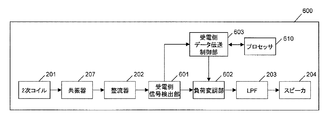
図1Bは、本実施の形態における無線電力データ伝送システム1の構成を示すブロック図である。無線電力データ伝送システム1は、送電器100と受電器200とを備えている。
FIG. 1B is a block diagram showing a configuration of wireless power
送電器100は、オーディオ信号ソース101、パルス幅変調部102、高周波変調部106、E級増幅器103、共振器104、および1次コイル105を有している。受電器200は、2次コイル201、共振器207、整流器202、LPF203、およびスピーカ204を有している。なお、図1Bでは図示していないが、送電器100は、交流電源またはバッテリなどの直流電源、あるいは図示していない他の無線電力伝送システムからの無線電力伝送により給電されている。
The
図1Bに示す無線電力データ伝送システム1は、オーディオ信号の伝送形式としてパルス幅変調(PWM:Pulse Width Modulation)を用いて、電力とオーディオ信号とを送電器100から受電器200に伝送する。パルス幅変調は、オーディオ信号の値をパルスの幅に変調して伝送する変調方式であり、2値の振幅レベルでオーディオ信号を伝送できることが特徴である。そのため、信号増幅の際にトランジスタの飽和領域を使用するE級増幅器103のような増幅器を使用することができるので、回路の小型化・低消費電力化が可能となる。オーディオ信号を重畳した無線電力伝送において、オーディオ信号形式にパルス幅変調を用いることにより、歪の少ない高品質なオーディオ信号伝送を実現できる。
The wireless power
また、無線電力データ伝送システム1は、送電器100から受電器200に電力およびオーディオ信号を伝送する方式として磁気共鳴型の電力伝送方式を使用する。磁気共鳴型の電力伝送方式によれば、高いQ値の共振器を用いることにより、送電器100と受電器200との距離が長い場合のように、結合係数kが小さい場合であっても高い効率の電力伝送が可能である。
Further, the wireless power
無線電力伝送システム1は、パルス幅変調されたオーディオ信号および電力を、1次コイル105と2次コイル201との間に発生する共振磁場の結合によって伝送する。
The wireless
以下、送電器100および受電器200の各構成要素を説明する。まず、送電器100の各構成要素を説明する。
Hereinafter, each component of the
オーディオ信号ソース101は、アナログまたはディジタルのオーディオ信号を発生させ、パルス幅変調部102に送出する回路である。オーディオ信号ソース101は、例えば不図示の記録媒体や、電波などの伝送媒体から取得した信号に基づき、オーディオ信号を生成する。
The
パルス幅変調部102は、オーディオ信号ソース101から入力されたオーディオ信号に対してパルス幅変調処理を行う回路である。パルス幅変調部102は、例えばLSI、DSP、FPGAといったプロセッサを含む。パルス幅変調部102は、パルス幅変調により、オーディオ信号の大きさに応じて幅が変調されたパルス列(以下、「PWMパルス」と呼ぶことがある。)を出力する。より具体的には、アナログオーディオ信号に対しては、入力信号を所定の周期および振幅をもつ三角波やノコギリ波のような参照波と比較することにより、入力信号を、その値に応じて異なる幅をもつパルス列に変換して出力する。一方、ディジタルオーディオ信号に対しては、後述するように、ディジタル信号処理によってパルス幅を変調させる。
The pulse
高周波変調部106は、パルス幅変調部102に接続され、PWMパルスを共振器104の共振周波数f0と同一の周波数の高周波(例えば、数MHz〜数十MHz)に変調する発振回路である。高周波に変調されたパルス列(以下、「高周波PWMパルス」と呼ぶことがある。)は、E級増幅器103に送出される。
The high
E級増幅器103は、高周波変調部106から出力された高周波PWMパルスを増幅して出力する増幅回路である。E級増幅器103は、例えば図2に示す構成を有している。E級増幅器103は、MOSFETなどのトランジスタから構成されるスイッチング素子Trと、インダクタLc、L、L0と、キャパシタC、C0とを有している。インダクタL、L0およびキャパシタC0は、共振器104の共振周波数f0と同一の共振周波数をもつ直列共振回路を構成する。スイッチング素子Tr、キャパシタC、直列共振回路(L、L0、およびC0)は、インダクタLcに対して並列に接続される。
The
図2に示す端子(a)には、高周波変調部106から高周波PWMパルスが入力される。また、端子(b)には、外部の直流電源(不図示)から、駆動電圧Vddが入力される。スイッチング素子Trのゲートに周波数f0の高周波PWMパルスを印加することにより、直流電源から供給される直流電力を周波数f0の高周波(RF)電力に変換することができる。これにより、電力伝送に必要な電力にまで増幅されたパルス列が、端子(c)から出力され、共振器104へ送られる。
A high frequency PWM pulse is input from the
なお、使用する増幅回路の種類は、E級増幅回路に限らず、トランジスタのスイッチング原理を利用するものであれば他の種類の増幅回路であってもよい。例えば、D級増幅回路やF級増幅回路のように、一般にスイッチング増幅器や飽和増幅器と呼ばれる回路であれば、同様に適用することができる。 Note that the type of amplifier circuit to be used is not limited to the class E amplifier circuit, and other types of amplifier circuits may be used as long as they utilize the transistor switching principle. For example, a circuit generally called a switching amplifier or a saturation amplifier, such as a class D amplifier circuit or a class F amplifier circuit, can be similarly applied.
共振器104は、共振周波数f0のLC共振回路である。共振器104は、インダクタとキャパシタとを有している。キャパシタは、良好な導電率を有する銅や銀などの導電対から好適に形成され得る。キャパシタには、例えばチップ形状、リード形状を有する、あらゆるタイプの素子を利用できる。共振器104は、1次コイル105を介して空間に周波数f0の共振磁場を形成する。
The
1次コイル105は、増幅されたパルス列に基づく電力およびデータを空間に送出するための要素である。1次コイル105の形状は、特に限定されず、ループ形状やスパイラル形状といった公知の形状を採用し得る。また、1次コイル105のサイズは、伝送距離や伝送電力に依存し、例えば数cm〜数十cmに設定される。
The
続いて、受電装置200の各構成要素を説明する。
Next, each component of the
2次コイル201は、送電装置100における1次コイル105と同様の構造、形状を有するコイルである。
The
共振器207は、送電側の共振器104と同一の共振周波数をもつ共振回路である。共振器207は、2次コイル201を介して、1次コイル105によって形成された共振磁場から電力を受け取る。
The
整流器202は、共振器207が受け取った電力を直流電力に変換する整流回路である。整流回路の構成は特に限定されず、公知のものを採用することができる。整流器202によって整流された直流電力は、ローパスフィルタ(LPF)203に送出される。
The
LPF203は、入力された信号の高周波数帯域成分を除去する低域通過フィルタである。受信パルス列から高周波数帯域成分を取り除くことにより、オーディオ信号が生成される。生成されたオーディオ信号はスピーカ204に入力され、そこで再生される。
The
以下、電力およびオーディオ信号を伝送する際の無線電力伝送システム1の動作を説明する。
Hereinafter, the operation of the wireless
送電器100におけるオーディオ信号ソース101は、受電器200のスピーカ204によって再生されるオーディオ信号をパルス幅変調部102に出力する。オーディオ信号ソース101は、出力信号としてアナログオーディオ信号、または標本化周波数fsおよび量子化ビット数bqで表されるディジタルオーディオ信号をパルス幅変調部102に出力する。パルス幅変調部102は、オーディオ信号ソース101から入力されたオーディオ信号をパルス幅変調する。
The
まず、オーディオ信号ソース101がアナログオーディオ信号を出力する場合のパルス幅変調部102の処理の一例について説明する。図3は、オーディオ信号ソース101から送られてくるオーディオ信号がアナログ信号の場合のパルス幅変調の例を示す図である。パルス幅変調では、入力されたオーディオ信号30は、周期が数マイクロ秒(周波数:数百kHz〜数MHz)、振幅がAtr1の三角波41と比較される。比較の結果、三角波41の値よりもオーディオ信号の値の方が大きい期間のみ、正の値をもつパルスが出力される。なお、比較は、オーディオ信号の入力がない場合やオーディオ信号の値が0の場合にデューティ比が50%のパルスが出力されるように行われる。この処理により、オーディオ信号の大きさに応じたパルス幅のパルス列が生成される。
First, an example of processing of the pulse
続いて、オーディオ信号ソース101がディジタルオーディオ信号を出力する場合のパルス幅変調部102の処理の一例について説明する。オーディオ信号ソース101が出力するオーディオ信号が、fs[kHz]、bqビットで表現されるPCM(Pulse Code Modulation)信号である場合、パルス幅変調部102は、PCM信号に対し、オーバーサンプリング、ノイズシェイピング(ΔΣ変調)などのディジタル信号処理を施す。
Next, an example of processing of the pulse
図4は、パルス幅変調部102がディジタルオーディオ信号のパルス幅変調を行う場合の内部構成の一例を示すブロック図である。図4に示すとおり、パルス幅変調部102は、オーバーサンプリング部1020と、ΔΣ変調部1024と、パルス出力部1029とを備えている。オーバーサンプリング部1020は、ゼロ挿入部1021と、補間フィルタ部1022と、前置ホールド部1023とを有している。なお、前置ホールド部1023は設けられていなくてもよい。ΔΣ変調部1024は、再量子化部1025と、パルス幅計算部1026と、遅延部1027と、乗算部1028とを有している。
FIG. 4 is a block diagram illustrating an example of an internal configuration when the pulse
一例として、ディジタルオーディオ信号は、サンプリング周波数fs=48kHz、量子化ビット数bq=16ビットのPCM信号であり、16倍のオーバーサンプルおよび1次のデルタシグマ変調が行われた後、パルス幅変調が行われる場合を想定する。サンプリング周波数fs=48kHzであるため、PCM信号のサンプリング周期は、1/fs≒20.8μsecである。PCM信号は、まずオーバーサンプリング部1020におけるゼロ挿入部1021に入力される。
As an example, the digital audio signal is a PCM signal having a sampling frequency fs = 48 kHz and a quantization bit number bq = 16 bits. After 16 times oversampling and first-order delta-sigma modulation, pulse width modulation is performed. Assume that this is done. Since the sampling frequency fs = 48 kHz, the sampling period of the PCM signal is 1 / fs≈20.8 μsec. The PCM signal is first input to the zero
図5は、オーバーサンプリング部1020による処理を説明するための図である。図5(a)は、ゼロ挿入部1021に入力されるPCM信号の例を示している。ゼロ挿入部1021は、図5(b)に示すように、PCM信号が入力されると、次のPCM信号が入力されるまでの間に、15個の値が0のPCMデータを挿入する(ゼロ挿入処理)。ゼロ挿入部1021は、ゼロ挿入処理を行った後のPCM信号を、補間フィルタ部1022に出力する。補間フィルタ部1022は、ゼロ挿入されたPCM信号に対して補間フィルタ(またはインターポレーションフィルタ、低域通過フィルタ)処理を行う。その結果、図5(c)に示すように、ゼロ挿入したサンプル点に0ではない値が現れ、2つの48kHzのPCM信号のサンプル点が、768kHz(=48kHz×16)のサンプル点で補間される。前値ホールド部1023が設けられている場合、補間フィルタ部1022は、補間後のPCM信号を前値ホールド部1023に送る。前値ホールド部1023が設けられていない場合、補間フィルタ部1022は、補間後のPCM信号をΔΣ変調部1024における再量子化部1025に出力する。
FIG. 5 is a diagram for explaining processing by the
前値ホールド部1023は、補間後のPCM信号に対して前値ホールド処理を施す。前値ホールド処理を施すことにより、サンプリング周波数をさらに増加させることができる。例えばゼロ挿入部1021で8倍、前値ホールド部1023で4倍のオーバーサンプルをするといったように、オーバーサンプリング処理を分割することができる。この結果、補間フィルタ部1022の設計条件が緩和されるといったメリットがある。
The previous
ΔΣ変調部1024は、オーバーサンプリングされたPCM信号に対し、ΔΣ変調によるノイズシェイピングを行う。ノイズシェイピングとは、PCM信号の振幅レベル数Na(=2bq−1)が、パルス幅の分解能Npより大きい場合に生じる白色の(周波数依存性のない)再量子化雑音を、有色化して可聴周波数帯域外に集中させるための処理である。ここで、パルス幅の分解能Npは、パルス幅変調処理を行うプロセッサ(LSI、DSP、FPGA等)の処理能力に依存する数値である。
The
ΔΣ変調部1024における再量子化部1025は、オーバーサンプリング部1020から入力されたPCM信号の再量子化を行う。具体的には、振幅レベル数Naで量子化されているPCM信号を、パルス幅分解能NpのPCM値に量子化する(Na>Np)。再量子化部1025は、再量子化したPCM信号をパルス幅計算部1026に送る。パルス幅計算部1026は、再量子化部1025から送られてきた再量子化されたPCM信号と、乗算部1028から出力されるフィードバック成分の加算(減算)処理を行い、出力するパルスの幅を決定する。パルス幅計算部1026は、計算したパルス幅を、遅延部1027およびパルス出力部1029に送る。
The
遅延部1027は、パルス幅計算部1026の出力パルス幅を1パルス分遅延させ、遅延したパルスの値を乗算部1028に送る。乗算部1028は、遅延部1027によって遅延したパルス幅に対し、所定の係数を乗算してパルス幅計算部1026に出力する。
The
なお、遅延部1027がパルス幅計算部1026の出力パルス幅を1パルス分遅延させる構成は、一次のデルタシグマ変調を用いる場合の例である。例えばN次のデルタシグマ変調を用いる場合は、1パルス分、2パルス分、・・・Nパルス分のパルス幅だけそれぞれ遅延させ、遅延した各パルスの値を乗算部1028に出力するように構成される。
The configuration in which the
パルス出力部1029は、パルス幅計算部1026によって決定されたパルス幅をもつパルスを、高周波変調部106に出力する。なお、このとき出力されるパルスの振幅は一定である。
The
図1Bに示す高周波変調部106は、パルス幅変調部102から送られてきたPWMパルスを共振器104の共振周波数f0(数MHz〜数十MHz)と実質的に同一の周波数の高周波に変調した高周波PWMパルスをE級増幅器103に出力する。
1B modulates the PWM pulse sent from the pulse
E級増幅器103では、高周波PWMパルスによってトランジスタがスイッチングされ、これと外部から供給される直流電力(駆動電圧Vdd)により、入力されたパルスが、電力伝送に必要な電力にまで増幅される。E級増幅器103は、増幅処理を行ったパルス列を共振器104に送る。
In the
共振器104は、電力およびオーディオ信号によって変調され、増幅された高周波のパルス列を1次コイル105に送る。これにより、外部空間に共振磁場が形成される。
The
受電器200は、2次コイル201を介して入力される共振磁場のエネルギを、上記共振器104と同一の共振周波数f0を持つ共振器207で受け、受信信号を生成する。
The
整流器202は、正の値と負の値の振幅を取りうる高周波交流信号である受信PWMパルスを包絡線検波、整流し、正の値の振幅のみを取る受信信号に変換する。整流器202で整流された受信信号は、LPF203に送られる。
The
LPF203は、低域通過フィルタであり、入力された受信パルス列から高周波数帯域成分を取り除く。受信パルス列から高周波数帯域成分を取り除くことにより、オーディオ信号が生成される。LPF203は、オーディオ信号をスピーカ204に送り、そこで音が再生される。
The
以上のように、本実施形態における無線電力データ伝送システム1は、パルス幅変調を行うことにより、オーディオ信号および電力を、無線で伝送する。このような構成により、ワイヤレススピーカを実現することができる。
As described above, the wireless power
<1−2.本論(電力、オーディオ信号、および制御信号の伝送)>
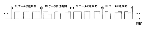
次に、これまでに説明した電力およびオーディオ信号の伝送に加えて、制御信号を伝送するためのワイヤレススピーカ装置の構成および動作を説明する。以下の説明では、送電器から受電器へのデータ伝送をフォワードリンク(FL)データ伝送、受電器から送電器へのデータ伝送をリターンリンク(RL)データ伝送と呼ぶ。
<1-2. Main Theory (Power, Audio Signal, and Control Signal Transmission)>
Next, in addition to the transmission of power and audio signals described so far, the configuration and operation of a wireless speaker device for transmitting control signals will be described. In the following description, data transmission from the power transmitter to the power receiver is referred to as forward link (FL) data transmission, and data transmission from the power receiver to the power transmitter is referred to as return link (RL) data transmission.
FLデータ伝送で伝送するFLデータの例としては、送電器のID、受電器のIDや定格、受信電力、消費電力の問い合わせ信号、受電器のパラメータ設定信号などがあり得る。また、伝送する情報は制御情報に限るものではなく、テキストデータ、画像データ、オーディオデータ等の情報でも良い。例えば、受電器に液晶ディスプレイ(LCD)のような表示デバイスが設けられている場合、表示デバイスに表示するための画像、テキストなどの情報が伝送され得る。 Examples of FL data transmitted by FL data transmission may include a power transmitter ID, a power receiver ID and rating, a received power, a power consumption inquiry signal, a power receiver parameter setting signal, and the like. Further, the information to be transmitted is not limited to the control information, but may be information such as text data, image data, audio data and the like. For example, when the power receiver is provided with a display device such as a liquid crystal display (LCD), information such as an image and text to be displayed on the display device can be transmitted.
また、RLデータの例としては、受電器のIDや定格、受信電力、消費電力の問い合わせに対する応答信号、送電器のパラメータ設定信号やエラーメッセージなどがあり得る。FLデータと同様、伝送する情報は制御情報に限定されず、どのような情報であってもよい。 Examples of the RL data may include a power receiver ID and rating, received power, a response signal to an inquiry about power consumption, a power transmitter parameter setting signal, an error message, and the like. Similar to the FL data, the information to be transmitted is not limited to the control information, and may be any information.
FLデータ伝送は、送電器において、FLデータの値に応じて高周波パルスの振幅を変動させることによって実現される。パルスの振幅の変動は、種々の方法が可能であるが、本実施形態では、E級増幅器に印加する直流電圧VddをFLデータの値に応じて変化させることによって行われる。 The FL data transmission is realized by changing the amplitude of the high frequency pulse in accordance with the value of the FL data in the power transmitter. Various methods can be used to change the amplitude of the pulse. In this embodiment, the DC voltage Vdd applied to the class E amplifier is changed according to the value of the FL data.
一方、RLデータ伝送は、受電器において、RLデータの値に応じて負荷を変動させることによって実現される。負荷が変化すると、送電器側のインピーダンスが変化するため、送電器の回路上に流れる電流および電圧も変化する。そこで、本実施形態における送電器は、回路上の適当な点で電流または電圧の変化を検出することにより、RLデータを検出する。このように、本実施形態では、受電器から送電器に直接RLデータが送信されるわけではないが、受電器側の負荷の変動により、送電器側において間接的にRLデータを検出できる。このため、本明細書では、上記のような間接的な方法によってRLデータを受電器から送電器に伝えることも、「RLデータ伝送」と呼ぶ。 On the other hand, the RL data transmission is realized by changing the load according to the value of the RL data in the power receiver. When the load changes, since the impedance on the transmitter side changes, the current and voltage flowing on the circuit of the transmitter also change. Therefore, the power transmitter in the present embodiment detects RL data by detecting a change in current or voltage at an appropriate point on the circuit. As described above, in the present embodiment, RL data is not directly transmitted from the power receiver to the power transmitter, but the RL data can be indirectly detected on the power transmitter side due to fluctuations in the load on the power receiver side. Therefore, in this specification, transmitting RL data from the power receiver to the power transmitter by the indirect method as described above is also referred to as “RL data transmission”.
FLデータおよびRLデータの伝送中は、送電器500から受電器600に伝送されるパルスの振幅が変動するため、電力伝送およびオーディオ信号の再生が不安定になる。そこで、本実施形態では、FLデータおよびRLデータの伝送中は、PWMパルスのパルス幅を調整することにより、一定の電力の伝送が維持されるように制御される。
During the transmission of the FL data and the RL data, the amplitude of the pulse transmitted from the
図6Aは、電力およびオーディオ信号に加えてFLデータおよびRLデータをさらに伝送することができるワイヤレススピーカシステム(無線電力データ伝送システム)に用いられる送電器500の構成例を示すブロック図である。図6Bは、当該システムに用いられる受電器600の構成例を示すブロック図である。
FIG. 6A is a block diagram illustrating a configuration example of a
送電器500は、オーディオ信号ソース101、共振器104、1次コイル105、高周波変調部106の他、図1Bに示すものとは機能が異なるパルス幅変調部501およびE級増幅器502を備えている。さらに、パルス幅の補正値を示す信号をパルス幅変調部501に送出する補正値算出部503と、駆動電圧Vddを決定してE級増幅器502に入力する駆動電圧制御部504と、E級増幅器502内を流れる信号を検出する送電側信号検出部505と、各部を制御する送電側データ伝送制御部506とを備えている。
The
本実施形態では、パルス幅変調部501、高周波変調部106、E級増幅器502、共振器104、および1次コイル105は、協働して本発明における「送電部」の機能を実現する。また、送電側データ伝送制御部506、補正値算出部503、駆動電圧制御部504、送電側信号検出部505は、協働して本発明における「(送電側)制御部」の機能を実現する。
In the present embodiment, the pulse
受電器600は、2次コイル201、共振器207、整流器202、LPF203、スピーカ204の他、整流器202によって整流された信号を検出する受電側信号検出部601と、負荷を変化させることができる負荷変調部602と、受電側信号検出部601から出力される信号に基づいて負荷変調部602を制御する受電側データ伝送制御部603とをさらに備えている。
The
本実施形態では、2次コイル201、共振器207、整流器202、受電側信号検出部601は、協働して本発明における「受電部」の機能を実現する。また、負荷変調部602は、本発明における「可変負荷」の機能を有する。受電側データ伝送制御部603は、本発明における「(受電側)制御部」の機能を有する。
In the present embodiment, the
以下、送電器500および受電器600の各要素を説明する。まず、送電器500の構成要素を説明する。
Hereinafter, each element of the
オーディオ信号ソース101、共振器104、1次コイル105、および高周波変調部106は、すでに説明した図1Bに示すものと同一なので説明を省略する。
Since the
パルス幅変調部501は、図1Bにおけるパルス幅変調部102に、パルス幅補正の機能を追加したものである。パルス幅変調部501は、補正値算出部503から入力される補正値を示す信号に基づき、オーディオ信号に基づくPWMパルスの幅を変化させることができる。例えば、入力されるオディオ信号がアナログ信号の場合、図3に示す三角波41の振幅Atr1または周波数f0を変化させることにより、パルス幅を変化させる。一方、オーディオ信号がディジタル信号の場合、図8を参照しながら後述する処理により、パルス幅を変化させる。
The pulse
E級増幅器502は、図2に示すE級増幅器103と同様の構成を有するが、複数の駆動電圧Vddに対応しており、駆動電圧Vddに比例した振幅EAの増幅された高周波PWMパルスを出力する。E級増幅器502の入力端子(b)には、駆動電圧制御部504から駆動電圧Vddが印加される。なお、E級増幅器502には、FLデータ伝送を行っていないときには、Vdd=Vdd0の駆動電圧が供給され、振幅EA0の増幅された高周波PWMパルスが出力される。一方、FLデータ伝送を行っているときには、FLデータの値に応じてVdd0とは異なる駆動電圧がE級増幅器502に供給される。その結果、E級増幅器502は、FLデータに応じて振幅が変調された高周波PWMパルスを共振器104に送出する。
The
補正値算出部503は、FLデータまたはRLデータに応じてパルスの振幅が変化しても、パルス面積が一定に保たれるように、パルス幅に加える補正値を計算してパルス幅変調部501に伝える。
The correction
駆動電圧制御部504は、送電側データ伝送制御部506から入力された制御信号に基づいて、駆動電圧Vddを決定し、決定した駆動電圧をE級増幅器502に入力する。駆動電圧制御部504は、例えば出力電圧の異なる複数の直流電源(電圧源)を用いて、制御信号に応じて使用する電圧源を切り替えることにより、駆動電圧の可変制御を実現することができる。あるいは、単一の電圧源の出力を、可変抵抗器等を用いて変動させることによって同様の制御を行ってもよい。
The drive
駆動電圧制御部504は、FLデータ伝送が行われていないときは、駆動電圧Vdd0をE級増幅器502に出力する。一方、駆動電圧制御部504は、FLデータ伝送期間中は、制御信号が示すFLデータの内容に応じて複数の駆動電圧から一つを選択し、E級増幅器502に出力する。例えば、FLデータ伝送を2値の振幅変調で行う場合、駆動電圧としてVdd1とVdd2の2つの値を、FLデータの内容によって切り替える。また、FLデータ伝送をN値(Nは3以上の整数)の振幅変調で行う場合は、N個の駆動電圧(Vdd1、Vdd2、・・・、VddN)を、FLデータに応じて切り替える。
The drive
送電側信号検出部505は、受電器600において負荷が変化した際に現れる、E級増幅器502内の電流・電圧の変化を観測するための検出器である。送電側信号検出部505は、E級増幅器502内の電流および電圧の少なくとも一方を観測することにより、受電器600における負荷の変化を検出し、検出結果(負荷変化検出信号)を送電側データ伝送制御部506に伝える。
The power transmission side
送電側データ伝送制御部506は、データ伝送の制御を行う回路である。送電側データ伝送制御部506は、CPUやマイコン、DSP、FPGAのようなプロセッサ510と接続されており、送信するデータの値を受け取る。なお、プロセッサ510は、送電器500の外部に設けられていてもよい。送電側データ伝送制御部506は、受電器600に伝送するFLデータに基づいて、制御信号を発生し、補正値算出部503および駆動電圧制御部504へ当該制御信号を送る。また、送電側データ伝送制御部506は、送電側信号検出部505から負荷変化検出信号を受け取り、当該検出信号に基づいて受電器600から送られてきたRLデータを検出する。このRLデータに基づき、送電側データ伝送制御部506は、後述するように、FLデータ伝送とRLデータ伝送との間の時分割の制御も行う。
The power transmission side data
続いて、図6Bに示す受電器600の各要素の構成を説明する。
Next, the configuration of each element of the
2次コイル201、整流器202、LPF203、スピーカ204、および共振器207はすでに説明した図1Bに示すものと同一なので説明を省略する。
The
受電側信号検出部601は、整流器202からの出力信号(受信パルス)の振幅を観測し、振幅変調されているFLデータを検出する回路である。受電側信号検出部601は、検出したFLデータを示す信号(振幅検出信号)を、受電側データ伝送制御部603に送出する。一方、整流器202から送られてきた受信パルスを負荷変調部602に送出する。
The power reception side
受電側データ伝送制御部603は、データ伝送の制御を行う回路である。受電側データ伝送制御部603は、CPUやマイコン、DSP、FPGAのようなプロセッサ610と接続されており、送電器500に送信するRLデータの内容を受け取る。なお、プロセッサ610は、受電器600の外部に設けられていてもよい。受電側データ伝送制御部603は、受け取ったRLデータに基づく制御信号を負荷変調部602に送る。また、受電側データ伝送制御部603は、受電側信号検出部601から振幅検出信号を受け取り、当該信号に基づいて送電器500から送られてきたFLデータを検出する。このFLデータに基づき、受電側データ伝送制御部603は、後述するように、FLデータ伝送とRLデータ伝送との間の時分割の制御も行う。
The power receiving side data
負荷変調部602は、受電側データ伝送制御部603から送られた信号が示すRLデータの内容に応じて、負荷を変化させる。負荷の変化のための構成として、例えば特許文献4の図2に記載されている構成を適用できる。特許文献4の記載全体を本願明細書に援用する。なお、負荷の変調の方法は特に限定されず、負荷変調の結果、パルスの振幅が変化する限り、公知のどのような方法を適用してもよい。負荷変調部602は、受電側信号検出部601から送られてきたパルスをLPF203に送出する。負荷変調部602によって負荷が変化すると、送電器500から受電器600へ伝送されるパルスの振幅が変化する。
The
次に、FLデータ伝送時およびRLデータ伝送時の送電器500および受電器600の動作について説明する。
Next, operations of
本実施形態におけるワイヤレススピーカ装置2は、受電器600のスピーカ204を駆動するための電力およびスピーカ204によって再生されるオーディオ信号を送電器500から受電器600に送ることに加えて、送電器500と受電器600との間で双方向のデータの伝送を行う。以下の説明では、送電器500から、受電器600のスピーカ204を駆動するための電力およびスピーカ204によって再生されるオーディオ信号が伝送されている状態、すなわち送電器500からパルスが送信されている状態を想定する。さらに、この状態において、FLデータ伝送およびRLデータ伝送は、時分割で行われる場合を想定する。
The
図7は、FLデータ伝送とRLデータ伝送とが時分割で行われる場合の例を示す図である。図7に示すように、FLデータ伝送期間とRLデータ伝送期間とは交互に設定される。この例では、FLデータ伝送期間およびRLデータ伝送期間は同じ長さであり、それぞれ3個のパルスが送られる。FLデータ伝送期間では、通常の形状のパルスが送電器500から受電器600に伝送される。一方、RLデータ伝送期間では、パルスの値が各パルスの持続時間の途中で変化したパルスが受電器600から送電器500に伝送される。このようなパルスの形状の変化により、RLのデータが表現される。
FIG. 7 is a diagram illustrating an example in which FL data transmission and RL data transmission are performed in a time division manner. As shown in FIG. 7, the FL data transmission period and the RL data transmission period are set alternately. In this example, the FL data transmission period and the RL data transmission period have the same length, and three pulses are sent each. In the FL data transmission period, a pulse having a normal shape is transmitted from the
なお、図7ではFLデータ伝送期間とRLデータ伝送期間とで、それぞれ3個のパルスを送る図が描かれているが、この例に限るものではない。FLデータの量および発生頻度とRLデータの量および発生頻度とに応じて、各期間が上記の例とは異なるように設定しても良い。また、FLデータ伝送期間とRLデータ伝送期間との比は、機器設計時やオーディオ信号伝送開始時、データ伝送開始時に決定する構成にしても良いし、データ伝送中に適応的に決定する構成にしても良い。また、必ずしもFLデータ伝送期間とRLデータ伝送期間とが交互に現れる必要はなく、途中にFLデータとRLデータとがいずれも伝送されていない期間(非データ伝送期間)を設けても良い。 Although FIG. 7 shows a diagram in which three pulses are transmitted in each of the FL data transmission period and the RL data transmission period, the present invention is not limited to this example. Depending on the amount and occurrence frequency of FL data and the amount and occurrence frequency of RL data, each period may be set to be different from the above example. The ratio between the FL data transmission period and the RL data transmission period may be determined at the time of device design, at the start of audio signal transmission, at the start of data transmission, or may be determined adaptively during data transmission. May be. Also, the FL data transmission period and the RL data transmission period do not necessarily appear alternately, and a period during which neither FL data nor RL data is transmitted (non-data transmission period) may be provided.
FLデータ伝送とRLデータ伝送との間の時分割の制御は、送電器500における送電側データ伝送制御部506および受電器600における受電側データ伝送制御部603が行う。
The time division control between the FL data transmission and the RL data transmission is performed by the power transmission side data
まず、FLデータ伝送期間における送電器500および受電器600の動作について説明する。なお、以下では、FLデータを2値(0/1)の振幅変調によって伝送する場合について説明する。FLデータをN値(Nは3以上の整数)の振幅変調によって伝送する場合についても容易に拡張可能であるため、そのような場合の説明は省略する。
First, operations of the
まず、オーディオ信号ソース101は、受電器600のスピーカ204で再生するオーディオ信号をパルス幅変調部501に送る。
First, the
送電側データ伝送制御部506は、プロセッサ510から送信すべきデータの内容を受け取る。送電側データ伝送制御部506は、FLデータ伝送期間中に、プロセッサから受け取ったデータを、無線電力データ伝送で伝送可能な形に変換することにより、FLデータを生成する。FLデータは、複数の0または1のビットからなるバイナリのデータ系列である。
The power transmission side data
送電側データ伝送制御部506は、FLデータの値(0/1)に応じて、補正値算出部503および駆動電圧制御部504に送る信号を変化させる。具体的には、送電側データ伝送制御部506は、FLデータが0のとき、補正値算出部503に「補正値P1」を指示する信号を送信し、駆動電圧制御部504に「駆動電圧Vdd1」を指示する信号を送信する。一方、送電側データ伝送制御部506は、FLデータが1のとき、補正値算出部503に「補正値P2」を指示する信号を送信し、駆動電圧制御部504に「駆動電圧Vdd2」を指示する信号を送信する。
The power transmission side data
以下、FLデータが0のとき、およびFLデータが1のときの各場合について、パルス列の変調動作をより具体的に説明する。 Hereinafter, the modulation operation of the pulse train will be described more specifically for each case where the FL data is 0 and the FL data is 1.
(1)FLデータが0のとき
送電側データ伝送制御部506は、補正値算出部503に「補正値P1」を示す制御信号を送り、駆動電圧制御部504に「駆動電圧Vdd1」を示す制御信号を送る。
(1) When FL Data is 0 The power transmission side data
補正値算出部503は、送電側データ伝送制御部506から送られてきた制御信号に基づき、パルス幅変調部501に、補正値P1を示す信号を送る。
The correction
パルス幅変調部501は、オーディオ信号ソース101から送られてきたオーディオ信号と、補正値算出部503から送られてきた補正値P1を示す信号とを用いてPWMパルスを生成する。以下、オーディオ信号がディジタルオーディオ信号(PCM信号)である場合における処理の例を説明する。
The pulse
図8は、この場合におけるパルス幅変調部501の構成例を示すブロック図である。パルス幅変調部501は、図4に示したパルス幅変調部102のパルス幅計算部1026を、パルス幅計算部801に置き換えたものである。パルス幅計算部801は、再量子化部1025から送られてくるPCM値と、乗算部1028から送られてくるフィードバック値と、補正値算出部503から送られてくる補正値P1とを加算または減算してパルス幅を計算し、パルス出力部1029および遅延部1027に送る。パルス幅変調部501は、PWMパルスを高周波変調部106に送る。
FIG. 8 is a block diagram illustrating a configuration example of the pulse
一方、オーディオ信号がアナログオーディオ信号の場合、パルス幅変調部501は、補正値算出部503から送られてきた補正値P1を示す信号に基づいて、図3に示す三角波41の振幅または周波数を変化させることにより、PWMパルスの幅を変化させる。なお、三角波41の代わりにノコギリ波のような参照波を用いる場合も、振幅または周波数を変化させることにより、同様の結果が得られる。パルス幅変調部501は、例えば不図示のメモリに、補正値と参照波の振幅または周波数との対応関係を規定した情報を予め記録しておき、その情報を参照することにより、上記の処理を実行する。
On the other hand, when the audio signal is an analog audio signal, the pulse
高周波変調部106は、パルス幅変調部501から送られてきたPWMパルスを共振器104の共振周波数f0(数MHz〜数十MHz)と実質的に同一の周波数の高周波に変調した高周波PWMパルスをE級増幅器502に出力する。
The high
駆動電圧制御部504は、送電側データ伝送制御部506より、「駆動電圧Vdd1」を示す制御信号を受けているので、E級増幅器502にVdd1の駆動電圧を供給する。
Since the drive
次に、E級増幅器502は、高周波変調部106から送られてきた高周波PWMパルスを用いてトランジスタのスイッチングを行い、増幅された高周波PWMパルスを出力する。ここで、増幅後高周波PWMパルスの振幅は、Vdd1に比例した値EA1となる。
Next, the
E級増幅器502は、増幅後高周波PWMパルスを共振器104に送る。増幅後高周波PWMパルスは、1次コイル105から、共振磁場として受電器600に伝送される。
The
(2)FLデータが1のとき
送電側データ伝送制御部506は、補正値算出部503に「補正値P2」を示す制御信号を送り、駆動電圧制御部504に「駆動電圧Vdd2」を示す制御信号を送る。
(2) When FL Data is 1 The power transmission data
補正値算出部503は、送電側データ伝送制御部506から送られてきた制御信号に基づき、パルス幅変調部501に、補正値P2を示す信号を送る。
The correction
パルス幅変調部501は、オーディオ信号ソース101から送られてきたオーディオ信号と、補正値算出部503から送られてきた補正値P2を示す信号とを用いてPWMパルスをし、高周波変調部106に送る。
The pulse
パルス幅変調部501の処理は、補正値がP1からP2に変わるだけで、それ以外についてはFLデータが0のときと同じなので、説明を省略する。
The processing of the pulse
高周波変調部106は、パルス幅変調部501から送られてきたPWMパルスを共振器104の共振周波数f0(数MHz〜数十MHz)と実質的に同一の周波数の高周波に変調した高周波PWMパルスをE級増幅器103に出力する。
The high
駆動電圧制御部504は、送電側データ伝送制御部506より、「駆動電圧Vdd2」を示す制御信号を受けているので、E級増幅器502にVdd2の駆動電圧を供給する。
Since the drive
次に、E級増幅器502は、高周波変調部106から送られてきた高周波PWMパルスを用いてトランジスタのスイッチングを行い、増幅された高周波PWMパルスを出力する。ここで、増幅後高周波PWMパルスの振幅は、Vdd2に比例した値EA2となる。
Next, the
E級増幅器502は、増幅後高周波PWMパルスを共振器104に送る。増幅後高周波PWMパルスは、1次コイル105から、共振磁場として受電器600に伝送される。
The
なお、上記説明では、Vdd0とVdd1とVdd2とはそれぞれ異なる値として記述をしたが、Vdd0=Vdd1、またはVdd0=Vdd2と設定することにより、0または1の値を伝送するときの駆動電圧を、非データ伝送期間の駆動電圧Vdd0と等しくしても良い。このようにすることで、補正値P1またはP2を0にすることができる。その結果、FLデータが0または1の一方の期間において、パルス幅変調部501、E級増幅器502の動作を、FLデータを伝送していない場合と同一にすることができ、構成を簡易化することができるので、望ましい実施の形態となる。そこで、以下では、Vdd0=Vdd1>Vdd2として説明を行う。このとき、0=P0=P1<P2、EA0=EA1>EA2という関係となる。
In the above description, Vdd0, Vdd1, and Vdd2 are described as different values. However, by setting Vdd0 = Vdd1, or Vdd0 = Vdd2, the driving voltage when transmitting a value of 0 or 1 is The drive voltage Vdd0 during the non-data transmission period may be equal. In this way, the correction value P1 or P2 can be set to zero. As a result, the operation of the pulse
本実施形態では、FLデータ伝送期間中、受電器600における受電側データ伝送制御部603は、負荷変調部602の負荷の制御を行わない。また、受電側データ伝送制御部603は、受電側信号検出部601に受信PWMパルスの振幅から受信FLデータ検出を指示する信号を送る。
In the present embodiment, the power receiving side data
FL伝送期間中、受電器600は、共振磁場を受け、受けた共振磁場を2次コイル201、共振器207、整流器202を通して、受信PWMパルスに変換する。
During the FL transmission period, the
受電側信号検出部601は、受信PWMパルスの振幅を検出する。受電側信号検出部601は、受信PWMパルスの振幅DAを予め設定されたしきい値TAと比較する。PWMパルスの振幅DAがTAより大きいと判定した場合、FLデータ0が伝送されたという情報を、TAより小さかいと判定した場合、FLデータ1が伝送されたという情報を受電側データ伝送制御部603に送る。なお、上記の信号検出方法は一例であり、他のパルス振幅変調の信号検出方法を用いても良い。
The power receiving side
受電側データ伝送制御部603は、受電側信号検出部601から送られてきたFLデータをデコードし、プロセッサ610に送る。また、受電側信号検出部601は、振幅検出後の受信PWMパルスを負荷変調部602に送る。FLデータ伝送中は、負荷変調部602は動作せず、固定負荷として機能する。その後、PWM信号はLPF203によりオーディオ信号に変換されスピーカ204から再生される。
The power receiving side data
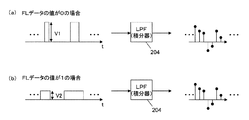
図9は、FLデータの値が0の場合とFLデータの値が1の場合とで、LPF204から出力されるオーディオ信号のレベルが変わらないことを示す図である。低域通過フィルタであるLPF204は、積分器で構成されるため、図9(a)、(b)に示すように、入力されるパルスの振幅が変化しても、その分パルス幅を大きくすることによって個々のパルスの面積(持続時間×値)が一定に維持されるため、積分器の出力は同一になる。
FIG. 9 is a diagram showing that the level of the audio signal output from the
以上が、FLデータ伝送時の送電器500および受電器600の動作の説明である。以上のように、本実施形態では、FLデータ伝送期間とRLデータ伝送期間とが時分割で交互に設定される。伝送するFLデータの値に応じてパルス振幅を変調させるとともに、各パルスの面積が一定に維持されるように、パルス幅を変化させることにより、電力およびオーディオ信号の安定的な伝送が可能となる。
The above is description of operation | movement of the
なお、上記の例では、各パルスの面積が一定になるようにパルス幅が変調されるが、厳密にパルス面積を一定にする必要はない。電力レベルの変化が小さくなるようにパルス幅を変化させるように制御されていれば、ある程度の効果を得ることができる。 In the above example, the pulse width is modulated so that the area of each pulse is constant, but the pulse area does not have to be strictly constant. If the control is performed so that the pulse width is changed so that the change in the power level is small, a certain effect can be obtained.
次に、RLデータ伝送時における送電器500および受電器600の動作を説明する。
Next, operations of the
RLデータ伝送が行われている間も、送電器500から受電器600へは、スピーカ204を駆動するのに十分な電力を持ったオーディオ信号が伝送されている。以下では、オーディオ信号伝送についての処理はすでに説明した通りなので、RLデータ伝送に関係する部分についてのみ説明する。
While RL data transmission is being performed, an audio signal having sufficient power to drive the
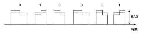
まず、受電器600の受電側データ伝送制御部603は、RLデータ伝送期間中、プロセッサ610から、送電器500に送信するデータの内容を受け取る。受電側データ伝送制御部603は、RLデータ伝送期間中、プロセッサ610から受け取ったデータを、無線電力データ伝送で伝送可能な形に変換することにより、RLデータを生成する。本実施形態におけるRLデータは、複数の0または1のビットからなるバイナリのデータ系列である。受電側データ伝送制御部603は、負荷変調部602にRLデータを伝送する。なお、RLデータは、2値のデータ系列である必要はなく、N値(Nは3以上の整数)のデータ系列であってもよい。N値のデータ系列を送信する場合、負荷値をN段階に変化させればよい。
First, the power receiving side data
負荷変調部602は、RLデータの内容に応じて、負荷の切り替えを行う。受電器600は、負荷切り替えの結果として生じるPWMパルス振幅の変化をもってRLデータの伝送を行う。
The
図10は、負荷変調によってパルス振幅が変化した様子を示す図である。図10に示すように、負荷変調部602は、PWMパルスの各々の持続時間(パルス幅で規定される時間)の中心時刻において、負荷を変化させる。また、負荷変調部602は、RLデータが0のときは、PWMパルス振幅が高い状態から、PWMパルスの中心時刻を境に低い状態に移るように、負荷を変化させる。一方、RLデータが1のときは、負荷変調部602は、PWMパルス振幅が低い状態から、PWMパルスの中心時刻を境に高い状態に移るように、負荷を変化させる。ここで、図10において、点線で示している振幅レベルは、負荷変調を行ったPWMパルスの平均振幅レベルを表す。平均振幅レベルは、FLデータ伝送およびRLデータ伝送共に行われていない場合の振幅レベルEA0よりも低くなる。
FIG. 10 is a diagram illustrating a state in which the pulse amplitude is changed by load modulation. As shown in FIG. 10, the
なお、図10に示すパルス波形は、送電側信号検出部505の観測地点におけるパルス波形を表している。負荷変化の影響が送電側信号検出部505に伝わるまでには若干の時間を要するため、負荷変調部602は、受電側信号検出部601が検出したパルスの中心時刻からその時間の分だけ早いタイミングで負荷を変化させる必要がある。この時間のずれは、システム設計時に予め測定され、補正される。
Note that the pulse waveform shown in FIG. 10 represents the pulse waveform at the observation point of the power transmission side
なお、本実施の形態では、負荷変調部602は一つのPWMパルス内で1回の振幅変化を行う構成としたが、振幅変化は1回に限るものではなく、2回以上の振幅変化があっても、RLデータが0のときと1のときとで振幅変化後のパルスの形状が異なっていればよい。また、本実施形態では、各パルスの持続時間の中心時刻で振幅が変化するように負荷が制御されるが、必ずしも中心時刻で振幅が変化するように制御する必要はない。
In the present embodiment, the
さらに、負荷変調部602は、一つのPWMパルスを一つのRLデータで変調する構成としたが、これに限るものではなく、複数のPWMパルスを一つのRLデータで変調する構成としても良い。このようにすることで、RLデータの伝送速度は低下するが、雑音、歪、同期ずれなどへの耐性を向上できる。
Furthermore, the
次に、RLデータ伝送時の送電器500の動作について説明する。
Next, the operation of the
送電側データ伝送制御部506は、RLデータ伝送期間中、補正値算出部503に補正値PRを送る。これは、前述の通り、受電器600の負荷変調部602での負荷変調により、PWMパルス振幅の平均値が、非データ伝送時のPWMパルス振幅より小さくなってしまうため、これをパルス幅で補正するために行う。補正値PRが入力されたパルス幅変調部501の動作は、FLデータ伝送時と補正値が異なるだけなので、説明を省略する。また、送電側データ伝送制御部506は、RLデータ伝送時、駆動電圧制御部504に駆動電圧を指定する信号は送信しないか、または、「駆動電圧Vdd0」を指示する信号を送信する。なお、本実施形態では、送電側データ伝送制御部506および補正値算出部503は、協働して「パルス幅補正部」の機能を実現する。
The power transmission side data
送電側データ伝送制御部506は、送電側信号検出部505が受電器600からのデータを検出したとき、送電側信号検出部505が受電側からのデータを検出したときのパルス列のパルス振幅と、当該データを検出していないときのパルス振幅とから求められる値に基づいて、パルス面積が一定に維持されるようにパルス幅を補正する。なお、パルス面積を一定に維持することが好ましいが、一定に維持されない場合であっても、パルス面積の変化を低減させるようにパルス幅が調整されれば、ある程度の効果を得ることができる。
The power transmission side data
以下、送電器500において、RLデータを検出する方法について説明する。
Hereinafter, a method of detecting RL data in the
E級増幅器502は、図2に示すE級増幅器103と同様、(a),(b),(c)の3つの入出力端子をもつ。端子(a)は、高周波PWM信号を入力する端子で、トランジスタTrに接続されている。端子(b)は、駆動電圧Vddを入力する端子で、送電側データ伝送制御部506からの指示によって、電圧Vdd0、Vdd1、Vdd2を切り替えて入力する。端子(c)は、増幅後高周波PWMパルスを出力する端子である。前述のように、受電器600の負荷が変化したとき、負荷変化の影響はE級増幅器502内で検出できる。具体的には、受電器600の負荷が変化すると、図2に示す電流Io、is、ig、iR、ic、および電圧vsが変化するので、これらのいずれかを観測することにより、受電器600における負荷変化によって表されるRLデータを検出することができる。送電側信号検出部505は、E級増幅器502内の電流または電圧の変化に基づいて、伝送されたRLデータが0であるか、1であるかを検出し、検出結果を送電側データ伝送制御部506に送る。
Similar to the
送電側データ伝送制御部506は、送電側信号検出部505から送られてきたRLデータをデコードし、プロセッサ510に送る。
The power transmission side data
図11は、本実施形態において、FLデータおよびRLデータの有無および値に応じて、送電器500によって設定されるパルス幅補正値、駆動電圧、増幅後PWMパルスの振幅がどのように設定されるかをまとめた表である。図11に示すように、FLデータおよびRLデータのいずれも伝送されていない期間は、パルス幅および駆動電圧はデフォルト値に設定される。FLデータ伝送時は、FLデータの値に応じて、駆動電圧およびパルス幅補正値が設定され、結果として増幅後PWMパルス振幅が変化する。一方、RLデータ伝送時は、RLデータの値によらず、パルス幅補正値が一定の値PRに設定される。
FIG. 11 shows how the pulse width correction value, the drive voltage, and the amplitude of the amplified PWM pulse set by the
なお、RLデータの値によらずにパルス幅補正値を一定値に設定するのは、個々のパルス面積が一定になるように受電器600内の負荷が制御されるためである。仮にRLデータの値に応じて、各パルスのパルス面積が変化するように構成されている場合、送電器500はパルス幅補正値をRLデータの値に応じて変えることが好ましい。また、各パルスのパルス面積が、仮にRLデータを伝送していないと仮定した場合のパルス面積と同一になるように負荷を変調させる構成も可能である。そのような構成は、若干の伝送ロスを伴うため、非効率であるが、送電器500によるパルス幅の調整が不要になるという利点がある。
The reason why the pulse width correction value is set to a constant value regardless of the value of the RL data is that the load in the
なお、受電器における負荷の変化は、上記のようなマンチェスタ符号に限らず、正弦波状または三角波状の変化であってもよい。例えば正弦波にすれば、負荷の制御が若干困難になるが、ノイズが減少するという利点がある。また、上記の説明では、オーディオ信号の伝送中にRLデータ伝送を行うこととしたが、RLデータ伝送は、オーディオ信号の停止時や再生時など、音量が0の期間のみに行うようにしてもよい。 Note that the load change in the power receiver is not limited to the Manchester code as described above, and may be a sine wave or triangular wave change. For example, using a sine wave makes it difficult to control the load, but has the advantage of reducing noise. In the above description, the RL data transmission is performed during the transmission of the audio signal. However, the RL data transmission may be performed only during a period in which the volume is 0, such as when the audio signal is stopped or reproduced. Good.
以上説明したように、本実施形態における送電器500および受電器600は、スピーカ204を駆動するために十分な電力を、オーディオ信号および双方向データ(RLデータおよびRLデータ)とともに単一の磁場搬送波で伝送することができる。本実施形態では、前述のとおり、双方向データであるFLデータおよびRLデータは、時分割で伝送される。
As described above, the
<1−3.TDDタイミング同期方法>
続いて、送電器500と受電器600との間でFLデータ伝送期間とRLデータ伝送期間(非データ伝送期間)との同期(以下TDD同期)を取るための方法の一例について説明する。
<1-3. TDD timing synchronization method>
Next, an example of a method for synchronizing the FL data transmission period and the RL data transmission period (non-data transmission period) (hereinafter referred to as TDD synchronization) between the
図12は、TDD同期を取る際に、送電器500が送信するパルスの様子を示す図である。送電器500は、オーディオ信号を送っていない場合、図12に示すようなTDD同期を取るためのパルスを送信する。ここで、オーディオ信号を送信していない場合とは、例えば、オーディオ再生前後や、曲間、送電器500の電源投入時である。オーディオ信号を送信していない場合は、オーディオ信号ソース101がPCM値0の信号を出力している場合に相当する。PCM値0に相当するPWMパルスは、デューティ比50%のパルスであり、デューティ比50%のパルスは、受電器600のスピーカ204からは無音として出力される。
FIG. 12 is a diagram illustrating a state of a pulse transmitted by the
図12に示すように、TDD同期時、送電器500は、Duty50%のパルスを送信している期間とパルスを送信していない期間とを交互に繰り返す。以下の説明では、Duty50%のパルスを送信している時間を「Duty50%パルス送信期間」、パルスを送信していない期間を「パルス非送信期間」と呼ぶ。送電器500は、FLデータ伝送期間と同じ時間だけ、Duty50%パルス送信期間を設け、RLデータ伝送期間と同じ時間だけパルス非送信期間を設けてパルスを送信する。このようにすることで、図12に示されるようなパルスを受信した受電器600は、パルスが送信されている期間と非送信の期間とを検出することができる。このため、FLデータ伝送期間とRLデータ伝送期間とを知ることができ、結果的にTDD同期を取ることができる。
As illustrated in FIG. 12, during TDD synchronization, the
また、上述のように、Duty50%パルス送信期間は、PCM値0のオーディオ信号を表しているので、受電器600のスピーカ204からは、音声は出力されない。また、パルス非送信期間においては、Duty0%のパルスは、負の方向に最大振幅のPCM値を現すが、連続して送ると受電器600における図示しない直流成分カットフィルタによりカットされ、スピーカ204へは入力されないため、音声は出力されない。ここで、パルスを送信しないことと、Duty0%のパルスを送信することとは同義である。このため、パルス非送信期間を、「Duty0%パルス送信期間」と考えることもできる。
Further, as described above, the
なお、上記説明ではDuty50%パルス送信期間をFLデータ伝送期間に、パルス非送信期間をRLデータ伝送期間に対応付けたが、この例に限るものではなく、対応付けを逆にしても同等の効果が得られる。
In the above description, the
また、受電器600は、図12に示すようなパルスを受信することにより、負荷変調の際に必要となるパルスの中心時刻を算定することができる。具体的には、Duty50%パルス送信期間においては、送信されるパルスはすべて同じパルス幅を持つので、各パルスの立上り時刻、立下がり時刻を検出し、そこから中心時刻を求めることができる。前後のパルスについても同様に中心時刻を求めることにより、中心時刻タイミングに同期したクロック信号が得られる。
In addition, the
なお、パルスの中心時刻を算定する場合は、必ずしも図12に示したようにDuty50%パルス送信期間と、パルス非送信期間を設ける必要はない。例えば、等しいDutyのパルスを一定期間連続して送るようにしても良い。このようにすることによっても、パルスの中心時刻に同期したクロック信号を抽出することができる。
When calculating the center time of a pulse, it is not always necessary to provide a
(実施の形態2)
次に、本発明の第2の実施の形態を説明する。実施の形態1では、E級アンプの駆動電圧を変化させることにより、PWMパルスの振幅を変化させるFLデータ伝送方法について説明した。本実施の形態では、FLデータ伝送方法の別の例として、E級アンプのスイッチング周波数を変化させることにより、PWMパルスの振幅を変化させるFLデータ伝送方法について説明する。以下の説明では、実施の形態1と同様の点については説明を省略し、異なる点を中心に説明する。
(Embodiment 2)
Next, a second embodiment of the present invention will be described. In the first embodiment, the FL data transmission method in which the amplitude of the PWM pulse is changed by changing the drive voltage of the class E amplifier has been described. In the present embodiment, as another example of the FL data transmission method, an FL data transmission method in which the amplitude of the PWM pulse is changed by changing the switching frequency of the class E amplifier will be described. In the following description, the same points as in the first embodiment will not be described, and different points will be mainly described.
図13は、本実施の形態における送電器1200の構成を示すブロック図である。本実施形態における送電器1200は、オーディオ信号ソース101、パルス幅変調部501、高周波変調部1201、E級増幅器103、共振器104、1次コイル105、送電側データ伝送制御部506、補正値算出部503、送電側信号検出部505を備えている。高周波変調部1201以外は、すでに説明した構成と同一なので、以下では高周波変調部1201の動作に関係する部分のみ説明する。
FIG. 13 is a block diagram illustrating a configuration of
実施の形態1における送電器500と同様、パルス幅変調部501は、PWMパルスを高周波変調部1201に送る。また、送電側データ伝送制御部506は、FLデータを高周波変調部1201に送る。
Similar to
高周波変調部1201は、2つの周波数を出力する発振器を備える。なお、これはFLデータ伝送を2値で行う場合の構成であり、3値以上で行う場合は、3つ以上の周波数を出力する発振器を用いればよい。また、発振器は、複数の周波数を出力可能な一つの発振器であっても良いし、発振周波数の異なる複数の発振器を有していてもよい。
The high
FLデータを伝送していない場合、およびFLデータ「0」を送信する場合の発振器の出力周波数をf0、FLデータ「1」を送信する場合の発振器の出力周波数をf1とする。高周波変調部1201は、送電側データ伝送制御部506から送られてくるFLデータの値に応じて、発振器の出力周波数をf0とf1との間で切り替える。その結果、FLデータの値に応じて周波数が変調された高周波変調PWMパルスが出力される。
When the FL data is not transmitted and when the FL data “0” is transmitted, the output frequency of the oscillator is f0, and when the FL data “1” is transmitted, the output frequency of the oscillator is f1. The high
ここで、発振器の出力周波数f0、f1と共振器104の周波数特性(ゲイン)との関係を図14に示す。図14に示すように、出力周波数f0は、共振器104の周波数特性のピークに近い部分、すなわち共振周波数付近の周波数であり、出力周波数f1は、共振器104の周波数特性のピークから少しずれた周波数である。このようにf0およびf1を設定することにより、高周波変調部1201およびE級増幅器103から出力されるパルスの振幅は一定であるが、FLデータの値に応じて、増幅後の高周波PWMパルスの周波数が変化するため、共振器104を通過後のパルスの振幅は、図14に示す周波数特性に応じて変化する。
Here, the relationship between the output frequencies f0 and f1 of the oscillator and the frequency characteristic (gain) of the
以上の構成により、送電器1200は、パルスの振幅の変化によってFLデータが「0」であるか「1」であるかを受電器600に伝送することができる。なお、この際、送電器1200の補正値算出部503は、実施の形態1の場合と同様、振幅変化によるオーディオ信号レベルの変化を打ち消すように補正値を算出し、パルス幅変調部501に送る。また、本実施形態における受電器は、実施の形態1で説明した受電器600と同一のものを用いることができる。
With the above configuration, the
以上のように、本実施の形態における送電器1200は、高周波変調部1201を備え、高周波PWMパルスを作成する際の発振周波数を、FLデータの値に応じて変化させる。このように構成することにより、E級増幅器103の駆動電圧Vddを変えることなく、増幅後の高周波PWMパルスの振幅を変えることができる。本実施形態では、単一の駆動電圧Vddに対応する増幅器でよいので、従来のE級増幅器を用いることができる。
As described above, the
なお、本実施形態における送電装置1200は、パルス幅変調部501から出力されるPWMパルスを高周波変調部1201によって高周波変調した後、E級増幅器103に入力するが、このような形態に限定されるものではない。例えば、パルス幅変調部501が、パルス幅変調および高周波変調の両方の処理を、同時、または後者を先に行ってもよい。その場合、送電側データ伝送制御部506は、周波数を変化させるための指示を、パルス幅変調部501に行うようにすればよい。
In the
上記の送電器1200は、高周波変調部1201の発振周波数と共振器104の周波数特性との関係を利用することにより、振幅変調を行う。上記の構成のほか、図15に示すように、高周波変調部の発振周波数は変えずに、周波数特性の異なる複数の共振回路を含む共振器1501を備え、FLデータの値に応じて使用する共振回路を切り替えるという構成をとっても、同等の効果を得ることができる。また、共振器1501の内部構成(コンデンサ、インダクタの値や数、接続形態)をFLデータの値に応じて変更することによって周波数特性(共振周波数)を変えるようにしてもよい。このように、共振器1501および一次コイル105を含むアンテナの共振周波数を制御することによって上記と同様の効果を実現できる。
The
なお、上記の実施の形態1、2では、送電器は、オーディオデータを伝送することを前提としたが、伝送されるデータはオーディオデータである必要はない。また、上記のオーディオデータのように、パルス幅変調されるデータを伝送することも必須ではない。送電器がパルス幅変調されるデータを伝送せず、電力およびFLデータだけを伝送する場合であっても上記と同様の制御を適用することが可能である。また、上記の説明では、FLデータ伝送およびRLデータ伝送の両方が行われるが、これらの両方が行われる必要は必ずしもない。送電器から受電器へのデータ伝送のみ、または受電器から送電器へのデータ伝送のみを行うように送電器および受電器が構成されていてもよい。 In the first and second embodiments, the power transmitter is assumed to transmit audio data. However, the transmitted data does not need to be audio data. Further, it is not essential to transmit data that is pulse width modulated like the audio data described above. Even when the power transmitter does not transmit data subjected to pulse width modulation and transmits only power and FL data, the same control as described above can be applied. In the above description, both FL data transmission and RL data transmission are performed, but it is not always necessary to perform both. The power transmitter and the power receiver may be configured to perform only data transmission from the power transmitter to the power receiver or only data transmission from the power receiver to the power transmitter.
本発明は、無線で電力を伝送して利用されるどのような電子機器にも適用することができる。例えば、ワイヤレススピーカ、ワイヤレステレビのような機器に有用である。 The present invention can be applied to any electronic device that is used by transmitting power wirelessly. For example, it is useful for devices such as wireless speakers and wireless televisions.
100 送電器
101 オーディオ信号ソース
102 パルス幅変調部
103 E級増幅器
104 共振器
105 1次コイル
106 高周波変調部
200 受電器
201 2次コイル
202 整流器
203 LPF
204 スピーカ
207 共振器
501 パルス幅変調部
502 E級増幅器
503 補正値算出部
504 駆動電圧制御部
505 送電側信号検出部
506 送電側データ伝送制御部
601 受電側信号検出部
602 負荷変調部
603 受電側データ伝送制御部
801 パルス幅計算部
1020 オーバーサンプリング部
1021 ゼロ挿入部
1022 補間フィルタ部
1023 前置ホールド部
1024 ΔΣ変調部
1025 再量子化部
1026 パルス幅計算部
1027 遅延部
1028 乗算部
1029 パルス出力部
1200 送電器
1201 高周波変調部
DESCRIPTION OF
Claims (16)
伝送すべき電力およびデータを重畳した複数のパルスからなるパルス列を送出する送電部と、
前記データの重畳による前記電力の変化を低減させるように前記送電部を制御する制御部と、
を備える送電装置。 A power transmission device used for wireless power data transmission for transmitting power and data wirelessly,
A power transmission unit for transmitting a pulse train composed of a plurality of pulses on which power and data to be transmitted are superimposed;
A control unit that controls the power transmission unit so as to reduce a change in the power due to the superimposition of the data;
A power transmission device comprising:
前記制御部からの指示に基づいて決定したパルス幅を有する第1のパルス列を出力するパルス幅変調器と、
前記第1のパルス列を増幅した第2のパルス列を前記パルス列として出力するパルス振幅変調器と、
前記第2のパルス列に基づく電力およびデータを送出する共振器と、
を有し、
前記制御部は、前記データの値に応じて前記第2のパルス列の振幅およびパルス幅を変化させるように、前記パルス幅変調器および前記パルス振幅変調器を制御する、
請求項1から3のいずれかに記載の送電装置。 The power transmission unit
A pulse width modulator for outputting a first pulse train having a pulse width determined based on an instruction from the control unit;
A pulse amplitude modulator that outputs, as the pulse train, a second pulse train obtained by amplifying the first pulse train;
A resonator for delivering power and data based on the second pulse train;
Have
The control unit controls the pulse width modulator and the pulse amplitude modulator so as to change the amplitude and pulse width of the second pulse train according to the value of the data;
The power transmission device according to any one of claims 1 to 3.
前記制御部は、前記データの値に応じて前記増幅器に入力する前記駆動電圧を切り替えることにより、前記第2のパルス列の振幅を変化させる、
請求項4に記載の送電装置。 The pulse amplitude modulator includes an amplifier that generates the second pulse train by amplifying the first pulse train according to an input drive voltage;
The control unit changes the amplitude of the second pulse train by switching the drive voltage input to the amplifier according to the value of the data.
The power transmission device according to claim 4.
前記制御部からの指示に基づいて決定したパルス幅を有する第1のパルス列を出力するパルス幅変調器と、
前記制御部からの指示に基づいて決定した周波数を有する、前記第1のパルス列を増幅した第2のパルス列を前記パルス列として出力するパルス振幅変調器と、
前記第2のパルス列に基づく電力およびデータを送出する共振器と、
を有し、
前記制御部は、前記データの値に応じて前記第1のパルス列の周波数を変化させるとともに、前記第1のパルス列のパルス幅を変化させるように前記パルス幅変調器を制御する、
請求項1から3のいずれかに記載の送電装置。 The power transmission unit
A pulse width modulator for outputting a first pulse train having a pulse width determined based on an instruction from the control unit;
A pulse amplitude modulator having a frequency determined based on an instruction from the control unit and outputting a second pulse train obtained by amplifying the first pulse train as the pulse train;
A resonator for delivering power and data based on the second pulse train;
Have
The controller changes the frequency of the first pulse train according to the value of the data and controls the pulse width modulator to change the pulse width of the first pulse train.
The power transmission device according to any one of claims 1 to 3.
前記制御部からの指示に基づいて決定したパルス幅を有する第1のパルス列を出力するパルス幅変調器と、
前記周波数変調部から出力された前記第1のパルス列を増幅した第2のパルス列を前記パルス列として出力するパルス振幅変調器と、
前記第2のパルス列に基づく電力およびデータを送出する少なくとも1つの共振器を含むアンテナと、
を有し、
前記制御部は、共振周波数を変化させるように前記アンテナを制御するとともに、前記第1のパルス列のパルス幅を変化させるように前記パルス幅変調器を制御する、
請求項1から3のいずれかに記載の送電装置。 The power transmission unit
A pulse width modulator for outputting a first pulse train having a pulse width determined based on an instruction from the control unit;
A pulse amplitude modulator that outputs, as the pulse train, a second pulse train obtained by amplifying the first pulse train output from the frequency modulator;
An antenna including at least one resonator for transmitting power and data based on the second pulse train;
Have
The control unit controls the antenna so as to change a resonance frequency, and controls the pulse width modulator so as to change a pulse width of the first pulse train.
The power transmission device according to any one of claims 1 to 3.
請求項8に記載の送電装置。 The controller sets the resonance frequency to a first frequency substantially equal to the frequency of the first pulse train when the data takes a first value, and takes the second value when the data takes a second value. Setting the resonance frequency to a second frequency different from the first frequency;
The power transmission device according to claim 8.
前記制御部は、前記複数の共振器の中から1つの共振器を選択することにより、前記アンテナの共振周波数を変化させる、
請求項8または9に記載の送電装置。 The at least one resonator includes a plurality of resonators having different resonance frequencies;
The control unit changes a resonance frequency of the antenna by selecting one resonator from the plurality of resonators.
The power transmission device according to claim 8 or 9.
前記送電部は、第2のデータをパルス幅変調して増幅することにより、前記電力、前記第1のデータ、および前記第2のデータを前記パルス列に変換して送出する、
請求項1から10のいずれかに記載の送電装置。 When the data is the first data,
The power transmission unit converts the power, the first data, and the second data into the pulse train by transmitting the second data by pulse width modulation and amplifying the data,
The power transmission device according to claim 1.
前記電力および前記データを送出する送電装置と、
前記送電装置から送出された前記電力および前記データを受け取る受電装置と、
を備え、
前記送電装置は、請求項1から15のいずれかに記載の送電装置である、
無線電力データ伝送システム。 A wireless power data transmission system for wirelessly transmitting power and data,
A power transmission device for transmitting the power and the data;
A power receiving device that receives the power and the data transmitted from the power transmitting device;
With
The power transmission device is the power transmission device according to any one of claims 1 to 15.
Wireless power data transmission system.
Priority Applications (2)
| Application Number | Priority Date | Filing Date | Title |
|---|---|---|---|
| JP2012086775A JP5891387B2 (en) | 2011-05-09 | 2012-04-05 | Wireless power data transmission system, power transmission device, and power reception device |
| US13/465,171 US9001881B2 (en) | 2011-05-09 | 2012-05-07 | Wireless power and data transmission system, power transmitting apparatus, and power receiving apparatus |
Applications Claiming Priority (3)
| Application Number | Priority Date | Filing Date | Title |
|---|---|---|---|
| JP2011103989 | 2011-05-09 | ||
| JP2011103989 | 2011-05-09 | ||
| JP2012086775A JP5891387B2 (en) | 2011-05-09 | 2012-04-05 | Wireless power data transmission system, power transmission device, and power reception device |
Publications (2)
| Publication Number | Publication Date |
|---|---|
| JP2012254003A true JP2012254003A (en) | 2012-12-20 |
| JP5891387B2 JP5891387B2 (en) | 2016-03-23 |
Family
ID=47141865
Family Applications (1)
| Application Number | Title | Priority Date | Filing Date |
|---|---|---|---|
| JP2012086775A Active JP5891387B2 (en) | 2011-05-09 | 2012-04-05 | Wireless power data transmission system, power transmission device, and power reception device |
Country Status (2)
| Country | Link |
|---|---|
| US (1) | US9001881B2 (en) |
| JP (1) | JP5891387B2 (en) |
Cited By (5)
| Publication number | Priority date | Publication date | Assignee | Title |
|---|---|---|---|---|
| WO2015008449A1 (en) * | 2013-07-18 | 2015-01-22 | パナソニック株式会社 | Orthogonal modulator |
| JP2015033316A (en) * | 2013-08-07 | 2015-02-16 | パイオニア株式会社 | Non-contact power supply device and computer program |
| JP2016527859A (en) * | 2013-07-24 | 2016-09-08 | ゼットティーイー コーポレーションZte Corporation | Wireless charging apparatus and method |
| KR101848984B1 (en) * | 2013-04-19 | 2018-04-13 | 캐논 가부시끼가이샤 | Power transmitting apparatus, method of controlling the same, and power transmission system |
| US10027169B2 (en) | 2015-03-23 | 2018-07-17 | Renesas Electronics Corporation | Wireless power supply system, power transmitting apparatus and power receiving apparatus |
Families Citing this family (27)
| Publication number | Priority date | Publication date | Assignee | Title |
|---|---|---|---|---|
| US9379777B2 (en) * | 2012-05-07 | 2016-06-28 | Nokia Technologies Oy | Near field communication circuitry used for hearing aid compatibility |
| JP6200167B2 (en) * | 2013-02-27 | 2017-09-20 | デクセリアルズ株式会社 | Power receiving device, received power adjusting method, received power adjusting program, and semiconductor device |
| JP6334958B2 (en) * | 2013-04-04 | 2018-05-30 | キヤノン株式会社 | Power transmission apparatus, control method thereof, and program |
| US9197172B2 (en) * | 2013-09-17 | 2015-11-24 | Qualcomm Incorporated | Switched mode high linearity power amplifier |
| KR101631669B1 (en) | 2014-08-06 | 2016-06-17 | 주식회사 맵스 | Magnetic resonance wireless power transmitting apparatus for tuning resonance frequency |
| CN108474817B (en) * | 2018-02-22 | 2021-06-01 | 廖淑辉 | Micro signal detection device and detection method thereof |
| US10277061B1 (en) | 2018-03-08 | 2019-04-30 | Nxp B.V. | Wireless device |
| DE102018212957B3 (en) | 2018-08-02 | 2020-01-02 | Fraunhofer-Gesellschaft zur Förderung der angewandten Forschung e.V. | TRANSFER OF DATA FROM ONE USER TERMINAL TO ANOTHER DEVICE |
| US11061456B2 (en) | 2019-01-23 | 2021-07-13 | Cisco Technology, Inc. | Transmission of pulse power and data over a wire pair |
| US10790997B2 (en) | 2019-01-23 | 2020-09-29 | Cisco Technology, Inc. | Transmission of pulse power and data in a communications network |
| JP7039515B2 (en) | 2019-03-15 | 2022-03-22 | 株式会社東芝 | Transmission equipment, contactless power transmission system and contactless power transmission method |
| US11063630B2 (en) | 2019-11-01 | 2021-07-13 | Cisco Technology, Inc. | Initialization and synchronization for pulse power in a network system |
| US10892800B1 (en) | 2020-01-06 | 2021-01-12 | Nucurrent, Inc. | Systems and methods for wireless power transfer including pulse width encoded data communications |
| US11303164B2 (en) | 2020-07-24 | 2022-04-12 | Nucurrent, Inc. | Low cost communications demodulation for wireless power transmission system |
| US11303165B2 (en) | 2020-07-24 | 2022-04-12 | Nucurrent, Inc. | Low cost communications demodulation for wireless power receiver system |
| WO2022088075A1 (en) * | 2020-10-30 | 2022-05-05 | 中国科学院深圳先进技术研究院 | Wireless energy-carrying message transceiving system, method, and device |
| CN112422158B (en) * | 2020-10-30 | 2021-08-20 | 中国科学院深圳先进技术研究院 | System, method and equipment for transmitting and receiving energy-carrying wireless message |
| US11938875B2 (en) * | 2020-12-18 | 2024-03-26 | Toyota Motor Engineering & Manufacturing North America, Inc. | System and method for wireless power transfer and data modulation for vehicles |
| US11277034B1 (en) | 2021-02-01 | 2022-03-15 | Nucurrent, Inc. | Systems and methods for receiver beaconing in wireless power systems |
| US11277035B1 (en) | 2021-02-01 | 2022-03-15 | Nucurrent, Inc. | Automatic gain control for communications demodulation in wireless power transmitters |
| US11811244B2 (en) * | 2021-02-01 | 2023-11-07 | Nucurrent, Inc. | Automatic gain control for communications demodulation in wireless power transmitters |
| US11431205B2 (en) | 2021-02-01 | 2022-08-30 | Nucurrent, Inc. | Systems and methods for receiver beaconing in wireless power systems |
| US11431204B2 (en) | 2021-02-01 | 2022-08-30 | Nucurrent, Inc. | Automatic gain control for communications demodulation in wireless power transfer systems |
| US11569694B2 (en) | 2021-02-01 | 2023-01-31 | Nucurrent, Inc. | Automatic gain control for communications demodulation in wireless power receivers |
| US11277031B1 (en) | 2021-02-01 | 2022-03-15 | Nucurrent, Inc. | Automatic gain control for communications demodulation in wireless power transmitters |
| US11595027B2 (en) * | 2021-03-01 | 2023-02-28 | Nxp Usa, Inc. | High frequency pulse width modulation shaping |
| CN116111738A (en) * | 2023-02-09 | 2023-05-12 | 兆赫兹(深圳)科技有限公司 | Transmitter of wireless power transmission system |
Citations (4)
| Publication number | Priority date | Publication date | Assignee | Title |
|---|---|---|---|---|
| JPH03505148A (en) * | 1988-04-11 | 1991-11-07 | ユニスキャン リミテッド | Actuators and communication systems |
| JPH05316003A (en) * | 1992-05-08 | 1993-11-26 | Omron Corp | Contactless communication system |
| WO2005069503A1 (en) * | 2004-01-16 | 2005-07-28 | Mitsubishi Denki Kabushiki Kaisha | Power supply device and power supply method |
| US20070194749A1 (en) * | 2006-02-22 | 2007-08-23 | Brad Albert Delanghe | Contact-less communication system |
Family Cites Families (21)
| Publication number | Priority date | Publication date | Assignee | Title |
|---|---|---|---|---|
| US4388716A (en) | 1979-11-15 | 1983-06-14 | Fuji Electric Co., Ltd. | Two-way transmission system |
| JPS58101591A (en) | 1981-12-14 | 1983-06-16 | Tamura Electric Works Ltd | Signal transmission system |
| JPS60257773A (en) | 1984-05-31 | 1985-12-19 | Shinano Denki Kk | Control circuit of inverter |
| JPS6139708A (en) | 1984-07-31 | 1986-02-25 | Akai Electric Co Ltd | Power supply voltage fluctuation correcting method in pulse width modulation amplifier |
| JP3140936B2 (en) | 1995-03-24 | 2001-03-05 | 三菱電機株式会社 | Two-way simultaneous communication method, its communication device, and programmable controller using the communication method |
| JPH11239105A (en) | 1998-02-20 | 1999-08-31 | Hitachi Ltd | Optical transmitter and optical transmission system using it |
| US6169670B1 (en) | 1999-04-08 | 2001-01-02 | Hitachi, Ltd. | Inverter apparatus operatable over extended frequency range while suppressing output error |
| US6756881B2 (en) | 1999-12-08 | 2004-06-29 | Ed&D, Inc. | Multiplex bus interface system and method for transmitting and receiving power and data |
| US7113547B2 (en) | 2001-08-24 | 2006-09-26 | Matsushita Electric Industrial Co., Ltd. | Data communication system, controller device and data communication method |
| JP3838547B2 (en) * | 2001-12-11 | 2006-10-25 | 株式会社ルネサステクノロジ | Power supply device for high frequency power amplifier circuit |
| EP1429455A1 (en) | 2002-12-11 | 2004-06-16 | Dialog Semiconductor GmbH | Linearization of a PDM class-D amplifier |
| JP2004312594A (en) | 2003-04-10 | 2004-11-04 | Japan Radio Co Ltd | Class d amplifier circuit |
| US7408996B2 (en) | 2003-05-29 | 2008-08-05 | Teridian Semiconductor Corporation | Method and apparatus for synchronization of data in a transformer circuit |
| JP2006245345A (en) | 2005-03-03 | 2006-09-14 | Nec Corp | Semiconductor light receiving element |
| JP4807021B2 (en) | 2005-09-26 | 2011-11-02 | オンキヨー株式会社 | Switching amplifier |
| JP4274252B2 (en) | 2007-01-24 | 2009-06-03 | 株式会社デンソー | PWM output type sensor circuit |
| JP4308858B2 (en) | 2007-02-16 | 2009-08-05 | セイコーエプソン株式会社 | Power transmission control device, power reception control device, non-contact power transmission system, power transmission device, power reception device, and electronic equipment |
| JP4779991B2 (en) | 2007-02-20 | 2011-09-28 | セイコーエプソン株式会社 | Power transmission control device, power transmission device, electronic device, and non-contact power transmission system |
| JP5169208B2 (en) | 2007-12-21 | 2013-03-27 | ヤマハ株式会社 | Wireless speaker device |
| JP4572355B2 (en) * | 2008-06-10 | 2010-11-04 | セイコーエプソン株式会社 | Power transmission control device, power transmission device, non-contact power transmission system, and data determination method |
| US8461719B2 (en) | 2008-09-27 | 2013-06-11 | Witricity Corporation | Wireless energy transfer systems |
-
2012
- 2012-04-05 JP JP2012086775A patent/JP5891387B2/en active Active
- 2012-05-07 US US13/465,171 patent/US9001881B2/en active Active
Patent Citations (4)
| Publication number | Priority date | Publication date | Assignee | Title |
|---|---|---|---|---|
| JPH03505148A (en) * | 1988-04-11 | 1991-11-07 | ユニスキャン リミテッド | Actuators and communication systems |
| JPH05316003A (en) * | 1992-05-08 | 1993-11-26 | Omron Corp | Contactless communication system |
| WO2005069503A1 (en) * | 2004-01-16 | 2005-07-28 | Mitsubishi Denki Kabushiki Kaisha | Power supply device and power supply method |
| US20070194749A1 (en) * | 2006-02-22 | 2007-08-23 | Brad Albert Delanghe | Contact-less communication system |
Cited By (12)
| Publication number | Priority date | Publication date | Assignee | Title |
|---|---|---|---|---|
| KR101848984B1 (en) * | 2013-04-19 | 2018-04-13 | 캐논 가부시끼가이샤 | Power transmitting apparatus, method of controlling the same, and power transmission system |
| US9948148B2 (en) | 2013-04-19 | 2018-04-17 | Canon Kabushiki Kaisha | Power transmitting apparatus, method of controlling the same, and power transmission system |
| US10483809B2 (en) | 2013-04-19 | 2019-11-19 | Canon Kabushiki Kaisha | Power transmitting apparatus, method of controlling the same, and power transmission system |
| US11101703B2 (en) | 2013-04-19 | 2021-08-24 | Canon Kabushiki Kaisha | Power transmitting apparatus, method of controlling the same, and power transmission system |
| US11764620B2 (en) | 2013-04-19 | 2023-09-19 | Canon Kabushiki Kaisha | Power transmitting apparatus, method of controlling the same, and power transmission system |
| WO2015008449A1 (en) * | 2013-07-18 | 2015-01-22 | パナソニック株式会社 | Orthogonal modulator |
| JP2015023396A (en) * | 2013-07-18 | 2015-02-02 | パナソニック株式会社 | Orthogonal modulator |
| US9331635B2 (en) | 2013-07-18 | 2016-05-03 | Panasonic Corporation | Quadrature modulator |
| JP2016527859A (en) * | 2013-07-24 | 2016-09-08 | ゼットティーイー コーポレーションZte Corporation | Wireless charging apparatus and method |
| US9893558B2 (en) | 2013-07-24 | 2018-02-13 | Zte Corporation | Wireless charging device and method |
| JP2015033316A (en) * | 2013-08-07 | 2015-02-16 | パイオニア株式会社 | Non-contact power supply device and computer program |
| US10027169B2 (en) | 2015-03-23 | 2018-07-17 | Renesas Electronics Corporation | Wireless power supply system, power transmitting apparatus and power receiving apparatus |
Also Published As
| Publication number | Publication date |
|---|---|
| JP5891387B2 (en) | 2016-03-23 |
| US9001881B2 (en) | 2015-04-07 |
| US20120287985A1 (en) | 2012-11-15 |
Similar Documents
| Publication | Publication Date | Title |
|---|---|---|
| JP5891387B2 (en) | Wireless power data transmission system, power transmission device, and power reception device | |
| JP5789790B2 (en) | Power transmission device and wireless power transmission system | |
| JP5807215B2 (en) | Wireless power transmission audio system, transmitter device and speaker used therefor | |
| JP2012253746A (en) | Wireless power data transmission system, power transmission apparatus, and power reception apparatus | |
| KR102012688B1 (en) | Apparatus and method for data communication using wireless power | |
| EP2171860B1 (en) | Transmitter with adjustable transmit level for magnetic link | |
| US8027732B2 (en) | Integrated phase-shift power control transmitter for use with implantable device and method for use of the same | |
| JP4628142B2 (en) | Polar modulation transmitter, wireless communication device, and power supply voltage control method | |
| KR101151922B1 (en) | Low power output stage | |
| CN102195577A (en) | Class-D power amplifier | |
| Son et al. | Simultaneous data and power transmission in resonant wireless power system | |
| KR100556909B1 (en) | Power circuit for pam in a mobile phone | |
| US10715935B2 (en) | Hearing instrument comprising a magnetic induction antenna | |
| KR101701662B1 (en) | A transceiver for a hearing aid and a method for operating such a transceiver | |
| TW201328103A (en) | Wireless power supplying apparatus and method | |
| JP5927545B2 (en) | Amplifier and acoustic device including the amplifier | |
| KR100613861B1 (en) | Resonant transmitter using fsk modulation | |
| JP2007150590A (en) | Fm modulation apparatus | |
| WO2007085788A1 (en) | Amplifier control | |
| JP2019140523A (en) | Class D amplifier | |
| JP2010136121A (en) | Wireless microphone | |
| CN104579371A (en) | Frequency modulation transmitter used for wireless tour conductor explanation and method for broadcasting tour conductor explanation words | |
| JP2005033352A (en) | Transmitting circuit |
Legal Events
| Date | Code | Title | Description |
|---|---|---|---|
| A711 | Notification of change in applicant |
Free format text: JAPANESE INTERMEDIATE CODE: A711 Effective date: 20141003 |
|
| A621 | Written request for application examination |
Free format text: JAPANESE INTERMEDIATE CODE: A621 Effective date: 20141119 |
|
| A977 | Report on retrieval |
Free format text: JAPANESE INTERMEDIATE CODE: A971007 Effective date: 20150824 |
|
| A131 | Notification of reasons for refusal |
Free format text: JAPANESE INTERMEDIATE CODE: A131 Effective date: 20150901 |
|
| A521 | Written amendment |
Free format text: JAPANESE INTERMEDIATE CODE: A523 Effective date: 20151006 |
|
| TRDD | Decision of grant or rejection written | ||
| A01 | Written decision to grant a patent or to grant a registration (utility model) |
Free format text: JAPANESE INTERMEDIATE CODE: A01 Effective date: 20151027 |
|
| A61 | First payment of annual fees (during grant procedure) |
Free format text: JAPANESE INTERMEDIATE CODE: A61 Effective date: 20151105 |
|
| R151 | Written notification of patent or utility model registration |
Ref document number: 5891387 Country of ref document: JP Free format text: JAPANESE INTERMEDIATE CODE: R151 |