JP2012248982A - Antenna device and electronic appliance - Google Patents
Antenna device and electronic appliance Download PDFInfo
- Publication number
- JP2012248982A JP2012248982A JP2011117681A JP2011117681A JP2012248982A JP 2012248982 A JP2012248982 A JP 2012248982A JP 2011117681 A JP2011117681 A JP 2011117681A JP 2011117681 A JP2011117681 A JP 2011117681A JP 2012248982 A JP2012248982 A JP 2012248982A
- Authority
- JP
- Japan
- Prior art keywords
- antenna
- electrode
- antenna device
- display unit
- dielectric layer
- Prior art date
- Legal status (The legal status is an assumption and is not a legal conclusion. Google has not performed a legal analysis and makes no representation as to the accuracy of the status listed.)
- Withdrawn
Links
Images


Abstract
Description
本発明は、液晶パネル等の表示部と一体化された構成を有するアンテナ装置、および、このアンテナ装置を備えた電子機器に関する。 The present invention relates to an antenna device having a configuration integrated with a display unit such as a liquid crystal panel, and an electronic apparatus including the antenna device.
従来、衛星からの電波を受信するための受信装置の一例として、電波の受信端末として機能する平面型受信アンテナと、時計部と、を重ねて配置した形態のものが開示されている。この受信装置の例では、平面型受信アンテナと時計部とを単に重ねただけではなく、時計部のカバーガラスを平面型受信アンテナのアンテナ誘電体として用いる構成例が示されている。この構成によれば、受信装置の小型化を図ることが可能となった(例えば特許文献1)。 2. Description of the Related Art Conventionally, as an example of a receiving device for receiving radio waves from a satellite, a configuration in which a planar receiving antenna that functions as a radio wave receiving terminal and a clock unit are arranged in an overlapping manner is disclosed. In this example of the receiving device, a configuration example is shown in which the cover glass of the timepiece unit is used as an antenna dielectric of the flat type reception antenna, as well as the planar type reception antenna and the timepiece unit are simply overlapped. According to this configuration, it is possible to reduce the size of the receiving device (for example, Patent Document 1).
また、電子機器として、太陽電池アンテナを有し衛星からの電波を受信するためのGPS(Global Positioning System)機能付の電子時計が開示されていて、この電子時計は、電波および太陽光が透過する文字板の裏面側に、アンテナ部およびソーラーセル(太陽電池部)を配置する構成である。これにより、電子時計は、GPS電波の確実な受信を維持しながらも、時計として、従来とほぼ同等の装飾性や装着性を有することが可能である(例えば特許文献2)。 Further, as an electronic device, an electronic timepiece having a GPS (Global Positioning System) function for receiving radio waves from a satellite having a solar cell antenna is disclosed, and the electronic timepiece transmits radio waves and sunlight. It is the structure which arrange | positions an antenna part and a solar cell (solar cell part) in the back surface side of a dial plate. As a result, the electronic timepiece can have almost the same decoration and wearability as the timepiece while maintaining reliable reception of GPS radio waves (for example, Patent Document 2).
しかし、特許文献1における技術では、アンテナ誘電体としてカバーガラスを用いているため、カバーガラスの表面側、つまり時刻を視認する側、に導電性薄膜および導電性薄膜に給電するための給電端子等を設けてあり、それらが時刻の視認を妨げないような配置や耐擦性、耐食性等に考慮しなければならない、という制約があった。一方、特許文献2における技術では、電子時計に組み込み可能な太陽電池アンテナが開示されているが、この太陽電池アンテナは、時計内部の専用スペースに、アンテナ部および太陽電池部を設ける構成であり、そのため、電子時計のさらなる小型薄型化の推進が困難である、という課題があった。
However, in the technique in Patent Document 1, since the cover glass is used as the antenna dielectric, the conductive thin film, the power supply terminal for supplying power to the conductive thin film, and the like on the surface side of the cover glass, that is, the time viewing side, etc. There is a restriction that it must be taken into consideration in arrangement, rubbing resistance, corrosion resistance, etc. so that they do not interfere with visual recognition of time. On the other hand, in the technology in
本発明は、上記課題の少なくとも一部を解決するためになされたものであり、以下の適用例または形態として実現することが可能である。 SUMMARY An advantage of some aspects of the invention is to solve at least a part of the problems described above, and the invention can be implemented as the following application examples or forms.
[適用例1]本適用例に係るアンテナ装置は、誘電体層と、前記誘電体層の第1面に配置された第1アンテナ電極と、前記誘電体層の前記第1面に対して向かい合う第2面に配置された第2アンテナ電極と、を有しかつ、位置情報衛星からの電波を受信するアンテナ部と、前記誘電体層を基材として用いかつ、情報を表示する表示部と、を備える、ことを特徴とする。 Application Example 1 An antenna device according to this application example faces a dielectric layer, a first antenna electrode disposed on the first surface of the dielectric layer, and the first surface of the dielectric layer. A second antenna electrode disposed on the second surface, and an antenna unit that receives radio waves from a position information satellite; a display unit that uses the dielectric layer as a base material and displays information; It is characterized by comprising.
このアンテナ装置によれば、アンテナ装置は、アンテナ部と表示部とを有しており、アンテナ部は、第1アンテナ電極が誘電体層を介して第2アンテナ電極と対向している構成である。従来の表示部は、表示部を支持可能な強度を有する基材に形成される構成であるが、アンテナ装置では、表示部が形成される基材として、アンテナ部の誘電体層を用いている。つまり、アンテナ装置は、誘電体層が、表示部の基材の機能を兼用するように構成されており、従来の技術では必要であった基材および誘電体層の2構成要素を、誘電体層の1構成要素としたことが特徴である。この場合、第1アンテナ電極は、誘電体層に形成された表示部の任意の位置(任意の層間)へ配置すれば良く、表示部の視認を妨げないように配置すること等が容易である。これにより、アンテナ装置は、電波を受信しつつ、構成要素数を削減して小型薄型化を図ることが可能である。 According to this antenna device, the antenna device has an antenna part and a display part, and the antenna part has a configuration in which the first antenna electrode faces the second antenna electrode with the dielectric layer interposed therebetween. . The conventional display unit is configured to be formed on a base material having a strength capable of supporting the display unit. However, in the antenna device, the dielectric layer of the antenna unit is used as the base material on which the display unit is formed. . In other words, the antenna device is configured such that the dielectric layer also functions as the base material of the display unit, and the two constituent elements of the base material and the dielectric layer, which are necessary in the prior art, are divided into the dielectric material. It is characterized by being one component of the layer. In this case, the first antenna electrode may be arranged at an arbitrary position (an arbitrary layer) of the display unit formed on the dielectric layer, and it is easy to arrange the first antenna electrode so as not to disturb the visual recognition of the display unit. . Thus, the antenna device can reduce the number of components and reduce the size and thickness while receiving radio waves.
[適用例2]上記適用例に係るアンテナ装置において、前記第1アンテナ電極は、平面視で前記表示部よりも大きな形状である、ことが好ましい。 Application Example 2 In the antenna device according to the application example described above, it is preferable that the first antenna electrode has a larger shape than the display unit in a plan view.
この構成によれば、アンテナ装置は、表示部の外形状よりも大きい設定であって、表示部がアンテナ装置に対して庇状に張り出しておらず、第1アンテナ電極の端部において、表示部の影響をほとんど受けることなく、電磁界を形成することが可能である。これにより、第1アンテナ電極は、表示部と一体の構成であっても、位置情報衛星からの電波を受信することが可能である。 According to this configuration, the antenna device is set to be larger than the outer shape of the display unit, and the display unit does not project in a bowl shape with respect to the antenna device, and at the end of the first antenna electrode, the display unit It is possible to form an electromagnetic field without being substantially affected by the above. Thereby, even if the 1st antenna electrode is a structure integrated with a display part, it is possible to receive the electromagnetic wave from a position information satellite.
[適用例3]上記適用例に係るアンテナ装置において、前記表示部は、複数の画素を有し、前記第1アンテナ電極は、平面視で前記複数の画素と画素との間に配置されている、ことが好ましい。 Application Example 3 In the antenna device according to the application example, the display unit includes a plurality of pixels, and the first antenna electrode is disposed between the plurality of pixels in a plan view. Is preferable.
この構成によれば、表示部は、複数の画素を有している。ここで、第1アンテナ電極は、画素の領域を避けて、平面視で画素と画素との間の部分に配置されている。これにより、アンテナ装置は、第1アンテナ電極が画素を避けて配置されていることにより、表示部の表示を暗くして見にくくするようなことを回避することが可能である。 According to this configuration, the display unit has a plurality of pixels. Here, the first antenna electrode is disposed in a portion between the pixels in plan view, avoiding the pixel region. Thereby, the antenna device can avoid making the display of the display unit dark and difficult to see because the first antenna electrode is arranged away from the pixels.
[適用例4]上記適用例に係るアンテナ装置において、前記誘電体層は、前記表示部の画素へ光を誘導する導光板である、ことが好ましい。 Application Example 4 In the antenna device according to the application example, it is preferable that the dielectric layer is a light guide plate that guides light to pixels of the display unit.
この構成によれば、導光板を備えた表示部は、画素へ光を誘導することにより、明るく均一な情報表示を行なえるようになっている。画素への光の誘導は、光源等から導光板を介して行なわれる。この導光板としては、例えばアクリル等の導光性体を好ましく用いることができ、ここで用いる導光性体は、独自の誘電率を有する誘電体でもある。従って、アンテナ装置では、表示部の導光板をアンテナ部の誘電体層として用いることが可能であり、従来の技術では必要であった導光板および誘電体層の2構成要素を、導光板の1構成要素としている。これにより、アンテナ装置は、構成要素数を削減して小型薄型化を確実に図ることが可能である。 According to this configuration, the display unit including the light guide plate can display bright and uniform information by guiding light to the pixels. The light is guided to the pixels from a light source or the like through a light guide plate. As this light guide plate, for example, a light guide material such as acrylic can be preferably used, and the light guide material used here is also a dielectric material having a unique dielectric constant. Therefore, in the antenna device, the light guide plate of the display unit can be used as the dielectric layer of the antenna unit, and two components of the light guide plate and the dielectric layer, which are necessary in the prior art, are combined with one of the light guide plates. As a component. As a result, the antenna device can be reliably reduced in size and thickness by reducing the number of components.
[適用例5]上記適用例に係るアンテナ装置において、前記表示部の配線は、前記第1アンテナ電極の受信用配線とは異なる配線によって前記表示部の領域内に配線されている、ことが好ましい。 Application Example 5 In the antenna device according to the application example described above, it is preferable that the wiring of the display unit is wired in the region of the display unit by a wiring different from the reception wiring of the first antenna electrode. .
この構成によれば、表示部の配線は、表示部の領域内にあることにより、該電磁界の形成を妨げないことに加え、位置情報衛星からの電波のような高周波信号に対してインダクタンスを有することになり、配線部分における該高周波信号を遮断する。つまり、配線部の影響で変化した不規則な高周波信号が第1アンテナ電極へ届かないようになっている。これにより、アンテナ装置は、表示部の配線の影響を受けず、表示部と一体であってもアンテナとしての性能を維持することが可能である。 According to this configuration, since the wiring of the display unit is within the region of the display unit, in addition to not hindering the formation of the electromagnetic field, an inductance is provided for a high-frequency signal such as a radio wave from a position information satellite. Therefore, the high-frequency signal in the wiring portion is blocked. That is, the irregular high frequency signal changed by the influence of the wiring portion does not reach the first antenna electrode. Accordingly, the antenna device is not affected by the wiring of the display unit, and can maintain the performance as an antenna even when integrated with the display unit.
[適用例6]上記適用例に係るアンテナ装置において、前記第1アンテナ電極は、平面視で前記表示部よりも小さな形状である、ことが好ましい。 Application Example 6 In the antenna device according to the application example described above, it is preferable that the first antenna electrode has a shape smaller than that of the display unit in plan view.
この構成によれば、第1アンテナ電極は、表示部と同等の大きさを含まず、表示部よりも小さい設定である。そのため、第1アンテナ電極の端部における電磁界は、表示部がアンテナ装置に対して庇状に張り出していることにより、表示部を透過して形成されるようになり、アンテナ装置の特性に影響を与える。この場合、アンテナ装置は、表示部がシート抵抗の高い傾向であり、かつ該電磁波が完全に遮断されることはなく、アンテナとして動作することは可能である。この構成では、第1アンテナ電極の外形を変えずに表示部の表示をできるだけ大きくしたい場合等において、有効に活用することが可能である。 According to this configuration, the first antenna electrode does not include the same size as the display unit and is set to be smaller than the display unit. For this reason, the electromagnetic field at the end of the first antenna electrode is formed through the display unit because the display unit projects in a hook shape with respect to the antenna device, which affects the characteristics of the antenna device. give. In this case, the antenna device tends to have a high sheet resistance, and the electromagnetic wave is not completely blocked and can operate as an antenna. With this configuration, it is possible to effectively utilize the display when it is desired to make the display unit display as large as possible without changing the outer shape of the first antenna electrode.
[適用例7]上記適用例に係るアンテナ装置において、前記第1アンテナ電極は、アンテナ共振周波数とのインピーダンス整合に用いるチューニング形状部を有している、ことが好ましい。 Application Example 7 In the antenna device according to the application example, it is preferable that the first antenna electrode has a tuning shape portion used for impedance matching with an antenna resonance frequency.
この構成によれば、アンテナ装置は、例えば切り込み状等をなしている、チューニング形状部を有することにより、アンテナ共振周波数を調整しアンテナとしての性能劣化を抑制することが可能である。 According to this configuration, the antenna device includes the tuning shape portion that has a cut shape or the like, for example, so that it is possible to adjust the antenna resonance frequency and suppress performance degradation as an antenna.
[適用例8]本適用例に係る電子機器は、上記適用例のいずれかに記載のアンテナ装置を備えている、ことを特徴とする。 Application Example 8 An electronic apparatus according to this application example includes the antenna device according to any one of the application examples.
この電子機器によれば、アンテナ装置は、誘電体層が、表示部の基材の機能を兼用する等の創意的構成であり、従来の技術に比べて使用要素数が削減されている。これにより、アンテナ装置を備えた電子機器は、電波受信の機能を果たし、且つ、より一層の小型薄型化を図ることが可能である。 According to this electronic apparatus, the antenna device has a creative configuration such that the dielectric layer also functions as the base material of the display unit, and the number of elements used is reduced as compared with the conventional technology. Accordingly, an electronic device including the antenna device can perform a function of receiving a radio wave and can be further reduced in size and thickness.
以下、本発明のアンテナ装置および電子機器における、好適な一例について、添付図面を参照して説明する。 Hereinafter, a preferred example of the antenna device and the electronic apparatus of the present invention will be described with reference to the accompanying drawings.
まず、位置情報衛星等の衛星からの電波による測位用信号等を受信して利用する通信システムの一例として、GPSシステムを取り上げ、その概要について説明する。 First, as an example of a communication system that receives and uses a positioning signal or the like from a radio wave from a satellite such as a position information satellite, a GPS system will be taken and its outline will be described.
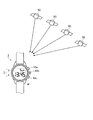
図1は、GPSシステムの概要を示す模式図である。図1に示すように、GPS衛星(位置情報衛星)90は、地球の上空の所定の軌道上を周回しており、例えば1.57542GHzのマイクロ波に航法メッセージ等を重畳させた、衛星信号を地上に送信している。このGPS衛星90は原子時計を搭載しており、衛星信号には原子時計で計時された極めて正確な時刻情報であるGPS時刻情報が含まれている。そのため、GPS受信機としての機能を備えた電子腕時計(電子機器)1は、衛星信号を受信して、内部時刻の進みまたは遅れを修正することにより、正確な時刻を表示することができる。この修正は、測時モードとして行なわれる。
FIG. 1 is a schematic diagram showing an outline of a GPS system. As shown in FIG. 1, a GPS satellite (positional information satellite) 90 orbits a predetermined orbit above the earth. For example, a satellite signal obtained by superimposing a navigation message or the like on a 1.57542 GHz microwave is transmitted. Sending to the ground. The
また、衛星信号にはGPS衛星90の軌道上の位置を示す軌道情報等も含まれている。つまり、電子腕時計1は、測位計算を行うこともでき、通常、4つ以上のGPS衛星90からそれぞれ送信された衛星信号を受信することによって、それら中に含まれる軌道情報およびGPS時刻情報を使用して測位計算を行う機能等を有している。測位計算により、電子腕時計1は、現在位置に合わせて時差を修正すること等が容易にでき、この修正は、測位モードとして行なわれる。このほか、衛星信号を利用すれば、現在位置表示、移動距離測定、移動速度計測を行う等の各種応用が可能であり、電子腕時計1では、これらの情報を、表示部である液晶表示部4によりデジタル表示することが可能である。なお、電子腕時計1は、液晶表示部4によるデジタル表示に限らず、アナログ表示や、デジタルとアナログとの併用表示等であっても良く、さらに、液晶以外の表示形態である表示部を用いることも可能である。
(実施形態1)
The satellite signal includes orbit information indicating the position of the
(Embodiment 1)
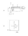
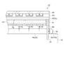
このような、GPS受信機能を備えた電子腕時計1について、その構成の一例を説明する。図2(a)は、実施形態1のアンテナ装置を備えた電子腕時計の構成を示す断面図、図2(b)は、アンテナ装置の構成を示す断面である。図2(a)および図1に示すように、GPS受信機能付きの電子腕時計1は、ステンレス鋼、チタン等の金属やプラスティック等の樹脂で構成された外装ケース11を備えている。外装ケース11は、この場合、略円筒状に形成され、時刻等の情報を視認する側である、表面側の開口に取り付けられたガラス12と、裏面側の開口に取り付けられた裏蓋13と、外装ケース11の側面に設けられたボタン16a,16b,16c(図1)と、を有している。これらボタン16は、手動操作により、液晶表示部4への表示の設定等ができるように構成されている。
An example of the configuration of such an electronic wristwatch 1 having a GPS reception function will be described. 2A is a cross-sectional view illustrating a configuration of an electronic wristwatch including the antenna device according to the first embodiment, and FIG. 2B is a cross-section illustrating a configuration of the antenna device. As shown in FIGS. 2A and 1, the electronic wristwatch 1 with a GPS reception function includes an
外装ケース11の内部には、時刻等を刻むための駆動機構や情報を処理して表示する処理機構等を有し、表面側が金属製で略円筒状をなすムーブメント15と、ムーブメント15の表面側に配置されたアンテナ装置2と、ムーブメント15に内蔵された電池18等が設けられている。アンテナ装置2は、GPS衛星90からの電波を受信するためのアンテナ部3と、アンテナ部3の表面側に配置され時刻等の情報を示すための液晶表示部4と、を有している。この電子腕時計の場合、アンテナ装置2のアンテナ部3および液晶表示部4は、矩形形状であり、外周が略円形状のリング11aの内周側に収容されている。
The
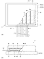
そして、アンテナ装置2におけるアンテナ部3のより詳細な構成は、この場合、図2(b)に示すように、ムーブメント15の表面側から順に、ムーブメント15の表面側の面15cである第2アンテナ電極3cと、誘電体層3bと、誘電体層3bを基材とし誘電体層3bに形成された液晶表示部4に設けられている透明な第1アンテナ電極3aと、から成っている。即ち、第1アンテナ電極3aと第2アンテナ電極3cとは、誘電体層3bを介して対向するように、誘電体層3bの第1面側または第2面側に位置している。また、ここでいう基材とは、後述する図3における基材4aが該当し、液晶表示部4を形成するための土台となる部材であり、且つ強度面で液晶表示部4を保持する役目を果たすものである。これらアンテナ装置2における個々の機能については、図5を参照して後述する。
In this case, the detailed configuration of the
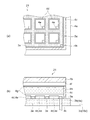
次に、液晶表示部4について説明する。図3(a)は、液晶表示部の構成を示す平面図であり、図3(b)は、液晶表示部の構成を示す断面図である。図3(b)は、図3(a)のP−P’に沿った断面図である。図3(a)および(b)において、液晶表示部4は、基材4aとしても機能している誘電体層3bと、誘電体層3bに形成されているパネル体とを有している。パネル体は、基材4a(誘電体層3b)と、基材4aと対をなす対向基板4bとが、封止材であるシール材4cによって貼り合わされている。このシール材4cは、両基板面内において、閉ざされた枠状の領域を形成している。
Next, the liquid
そして、液晶表示部4は、シール材4cによる枠状領域の内側に、モザイク状等をなし基材4a(誘電体層3b)の表面に配置されている複数の画素電極(画素)4dと、各画素電極4dをスイッチング制御するTFT(Thin Film Transistor)4eと、対向電極4fの基材4a側の面に画素電極4dに対向して配置されている平面状の対向電極4fと、画素電極4dおよび対向電極4fを覆うように形成されている配向膜4gと、シール材4cおよび配向膜4gによって区画された領域内に封入保持されている液晶4hと、を有している。これら画素電極4d、TFT4e、対向電極4fおよび配向膜4gは、透明部材により形成されている。液晶4hは、TFT4eによりスイッチング制御された画素電極4dに対応して、各種情報の表示をする。また、液晶表示部4は、端子部31を介して、外部との接続用のフレキシブル配線(配線)32を有している。
The liquid
そして、この場合、液晶表示部4の対向電極4fは、アンテナ部3の第1アンテナ電極3aとしての機能も果たす設定になっている。また、シール材4cには、第1アンテナ電極3aとして機能する対向電極4fへ高周波の給電をするための、給電体4kが配設されている。なお、これら対向電極4fおよび給電体4kについては、図5を参照して後述する。
In this case, the
ここで、アンテナ部3は、液晶表示部4の外形状と同じであって、液晶表示部4がアンテナ部3に対し外形方向へ張り出していない。そのため、第1アンテナ電極3aは、その端部において、液晶表示部4の影響をほとんど受けることなく、電磁界を形成することができる。これにより、第1アンテナ電極3aは、液晶表示部4と一体の構成であっても、電波受信部として位置情報衛星からの電波を確実に受信することができる。これは、アンテナ部3が液晶表示部4の外形状より大きい場合においても、同様なことが言える。
Here, the
また、液晶表示部4においては、使用する液晶4hの種類、つまり、TN(Twisted Nematic)モード、STN(Super Twisted Nematic)モード等の動作モードや、ノーマリホワイトモードまたはノーマリブラックモードの別に応じて、位相差板、偏光板等が所定の向きに配置されるが、ここでは図示を省略してある。また、液晶表示部4をカラー表示用として構成する場合には、対向基板4bにおいて、各画素電極4dに対向する領域に、赤(R)、緑(G)、青(B)のフィルターを設ければよい。さらに、液晶表示部4において、画素電極4dへ光を導いて、表示をより鮮明にするためのランプおよび導光板を設ける構成も考えられる。
Further, in the liquid
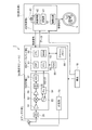
次に、GPS受信機能を備えた電子腕時計1の回路構成について説明する。図4は、電子腕時計の回路構成を示すブロック図である。電子腕時計1は、アンテナ部3と、受信モジュール30と、制御部40を含む表示部80と、電池18と、を含んで構成されている。
Next, a circuit configuration of the electronic wristwatch 1 having a GPS reception function will be described. FIG. 4 is a block diagram showing a circuit configuration of the electronic wristwatch. The electronic wristwatch 1 includes an
受信モジュール30は、アンテナ部3が接続されており、SAW(Surface Acoustic Wave:表面弾性波)フィルター35と、RF(Radio Frequency:無線周波数)部50と、ベースバンド部60と、を含んで構成されている。SAWフィルター35は、アンテナ部3が受信した信号から衛星信号を抽出する処理を行う。RF部50は、LNA(Low Noise Amplifier)51と、ミキサー52と、VCO(Voltage Controlled Oscillator)53と、PLL(Phase Locked Loop)回路54と、IF(Intermediate Frequency:中間周波数)アンプ55と、IFフィルター56と、ADC(A/D変換器)57と、を含んで構成されている。
The receiving module 30 is connected to the
SAWフィルター35が抽出した衛星信号は、LNA51で増幅され、ミキサー52でVCO53が出力するクロック信号とミキシングされて中間周波数帯の信号にダウンコンバートされる。PLL回路54は、VCO53の出力クロック信号を分周したクロック信号と基準クロック信号とを位相比較してVCO53の出力クロック信号を基準クロック信号に同期させる。ミキサー52でミキシングされた信号は、IFアンプ55で増幅され、IFフィルター56で高周波信号が除去される。IFフィルター56を通過した信号は、ADC(A/D変換器)57でデジタル信号に変換される。ベースバンド部60は、DSP(Digital Signal Processor)61と、CPU(Central Processing Unit)62と、SRAM(Static Random Access Memory)63と、RTC(リアルタイムクロック)64と、を含んで構成されている。また、ベースバンド部60には、温度補償回路付き水晶発振回路(TCXO:Temperature Compensated Crystal Oscillator)65やフラッシュメモリー66等が接続されている。
The satellite signal extracted by the
温度補償回路付き水晶発振回路(TCXO)65は、温度に関係なくほぼ一定の周波数の基準クロック信号を生成し、フラッシュメモリー66には、現在位置情報や時差情報等が記憶されている。ベースバンド部60は、測時モード等に設定されると、RF部50のADC57が変換したデジタル信号からベースバンド信号を復調する処理を行う。また、ベースバンド部60は、捕捉したGPS衛星90の航法メッセージに含まれる軌道情報やGPS時刻情報等の衛星情報を取得してSRAM63に記憶する。また、受信モジュール30には、第1アンテナ電極3aの給電体4kへ高周波の給電をするための、給電部70が設けられている。
A crystal oscillation circuit (TCXO) 65 with a temperature compensation circuit generates a reference clock signal having a substantially constant frequency regardless of temperature, and the
そして、表示部80は、制御部40および水晶振動子43等を含んで構成されている。制御部40は、記憶部41と、発振回路42と、駆動回路44とを備え、各種制御を行う。制御部40は、受信モジュール30を制御し、制御信号を受信モジュール30に送り、受信モジュール30の受信動作を制御すると共に、制御部40内の駆動回路44を介して液晶表示部4の駆動を制御する。記憶部41には内部時刻情報をはじめ各種情報が記憶されている。
The display unit 80 includes the control unit 40, the
ここで、電子腕時計1に内臓されているアンテナ装置2は、複数のGPS衛星90(図1)からの衛星信号を受信する必要がある。GPS衛星90から送信される衛星信号の電波は、いわゆる円偏波であるため、アンテナ装置2は、この円偏波を受信するのに適した、いわゆるパッチアンテナであることが望ましく、さらに、電子腕時計1に組み込めるように、コンパクトな形態であることが好ましい。そこで、アンテナ装置2は、電子腕時計1のアンテナ部3と液晶表示部4とを一体化した形態となっている。
Here, the
図5(a)は、アンテナ装置への給電構成を示す断面図であり、図5(b)は、第1アンテナ電極における励振モードを示す平面図である。図5に示すように、アンテナ装置2は、電気的導体部であり、いわゆるパッチアンテナのパッチ金属板である第1アンテナ電極3aと、ムーブメント15における誘電体層3bを受ける面15cでもある第2アンテナ電極3cと、第1アンテナ電極3aおよび第2アンテナ電極3cとの間に配置された誘電体層3bと、を有している。
Fig.5 (a) is sectional drawing which shows the electric power feeding structure to an antenna apparatus, FIG.5 (b) is a top view which shows the excitation mode in a 1st antenna electrode. As shown in FIG. 5, the
第1アンテナ電極3aは、通常、銅・アルミニウム・鉄・金・銀・パラジウム等の導体またはこれらの合金であれば機能するが、この場合、透明部材である必要があり、酸化インジュウムスズ(ITO:Indium Tin Oxide)等の透明導電性材を用いて矩形状に形成されている。そして、第1アンテナ電極3aは、既述したように、液晶表示部4の対向電極4fでもあって、アンテナ部3を構成すると共に液晶表示部4をも構成している。
The
また、誘電体層3bは、第1アンテナ電極3aとほぼ同じ大きさの矩形状であって、使用可能な材質としては、アルミナ(Al2O3)、ムライト(3Al2O3・2SiO2)、ステアライト(MgO/SiO2)、フォルステライト(2Mg2O/SiO2)、ジルコニア(PSZ)、チタン酸マグネシア(MgTiCO3)等が挙げられる。この誘電体層3bの特性としては、誘電率が8以上22以下が望ましく、誘電正接が0.001以下が望ましい。そこで、これらの特性を得るために、電子時計における誘電体層3bのサイズは、電子腕時計1のような矩形状の場合には一辺が2cm〜4cmであることが望ましい。参考に、誘電体層3bが円形である場合には直径が2.5cm〜3.5cmであることが望ましい。また、いずれの場合でも、厚さは、0.05mm〜1.5mmであることが望ましい。電子腕時計1において、アンテナ装置2の誘電体層3bは、厚さ0.5mm、縦2cmおよび横3cmの矩形状をなすチタン酸マグネシア(MgTiCO3)を用い、誘電率が17および誘電正接が0.001の特性を有している。
The
このような構成のアンテナ装置2において、第1アンテナ電極3aへ給電部70(図4)から電力供給をするために、給電体4kが設けられている。給電体4kは、第1アンテナ電極3aに対する所定位置に設けられている。給電体4kは、金属製の電気的導体であり、第1アンテナ電極3aと接続された状態で、シール材4cおよび誘電体層3bに挿通され、挿通された先端が絶縁体を介してムーブメント15(第2アンテナ電極3c)と非接触となるようにして、ムーブメント15へ装着されている。これにより、第1アンテナ電極3aへは、給電体4kを介して、給電部70から電力が供給され、同時に、第2アンテナ電極3cへも給電部70から電力が供給される。この場合、第2アンテナ電極3cは、アース側であり、いわゆる接地電極として機能する。また、給電体4kへの給電用配線は、第1アンテナ電極3aの受信用配線としても機能する。
In the
次に、アンテナ部3による、GPS衛星90からの測位用信号である電波の受信について説明する。GPS衛星90からの電波は、受信する対象が、移動体のように任意の方向を向いていても受信可能となるように、円偏波が用いられている。円偏波は、時間の経過と共に電界の方向が回転する形態のものである。一般に、アンテナは、電波の電界方向と同じ方向に電流が流れることにより、該電波を受信することができる。従って、円偏波を受信するためには、アンテナに流れる電流を時間の経過と共に、回転させることが肝要である。アンテナに流れる電流が回転するためには、直交する方向に電流を流し90度の位相差を持った励振を発生させれば良い。アンテナ部3では、第1アンテナ電極3aにおいて、以下に説明するようにして、互いに直交し90度の位相差を持った、2つの励振モードを発生させることにより、円偏波の受信を可能にしている。
Next, reception of radio waves that are positioning signals from the
図5(b)に示すように、アンテナ部3は、給電体4kの部分において給電を受けるピン給電方式である。この方式は、給電系に特別な回路素子等を用いることなく励振モードを発生させることができ、円偏波の受信が容易に行える簡便なものである。このような配置のアンテナ部3において、給電部70から給電体4kへ高周波の給電がなされると、第1アンテナ電極3aには、短辺方向に電流が流れ励振モードF1が発生し、励振モードF1と直交する方向には、長辺方向に電流が流れ励振モードF2が発生する。逆に言えば、アンテナ装置2の構成によって、上記のような励振モードF1,F2が発生するように、給電体4kを設定することが可能である。この時、励振モードF1と励振モードF2とが励振する間の長さは、第1アンテナ電極3aの矩形状により異なっており、短辺および長辺の長さを調整すれば、励振モードF1と励振モードF2とを異なる位相とする等の制御が容易に行なえる。
As shown in FIG.5 (b), the
以上説明したように、電子腕時計1におけるアンテナ装置2は、アンテナ部3の誘電体層3bを液晶表示部4の基材として兼用している。また、第1アンテナ電極3aが液晶表示部4の一部を兼ねており、即ち第1アンテナ電極3aが対向電極4fとしても機能している構成である。さらに、ムーブメント15の一部を第2アンテナ電極3cとして兼用している。これらにより、アンテナ装置2は、使用する構成要素数を削減することが可能となっている。また、アンテナ装置2は、電子腕時計1の内部で占める領域を、特に厚さにおいて、ほぼ最小限にすることが可能となり、電子腕時計1のデザイン等を制約せずに小型でき、且つ電波受信の機能を果たすことが可能である。
(実施形態2)
As described above, the
(Embodiment 2)
次に、アンテナ装置の他の形態について説明する。図6(a)は、実施形態2におけるメッシュ状の第1アンテナ電極を備えたアンテナ装置を示す平面図であり、図6(b)は、メッシュ状の第1アンテナ電極を示す断面図である。実施形態2におけるアンテナ装置21と、実施形態1におけるアンテナ装置2とは、受信部として機能する第1アンテナ電極3aの構成が異なっている。以下では、アンテナ装置21を構成する部品において、機能が同一なものには同一符号を付与してあり、実施形態1と異なる部分についてのみ説明する。
Next, another embodiment of the antenna device will be described. FIG. 6A is a plan view showing an antenna device provided with the mesh-shaped first antenna electrode in the second embodiment, and FIG. 6B is a cross-sectional view showing the mesh-shaped first antenna electrode. . The
図6(a)および(b)に示すように、アンテナ装置21における第1アンテナ電極3aは、モザイク状等に配置され互いに間をおいて並んでいる画素電極4dの部分を避けるようにして、設けられている。つまり、第1アンテナ電極3aは、各画素電極4dの間、即ち画素電極4dの間隙部分、に設けられていて、この場合、メッシュ状の形状になっている。そして、メッシュ状の第1アンテナ電極3aからは、給電体4kがムーブメント15の方向へ向けて配設されている。
As shown in FIGS. 6A and 6B, the
このような形態のアンテナ装置21は、第1アンテナ電極3aが画素電極4dを避けて配置されているため、液晶4hによる情報の表示をまったく妨げることがないと同時に、第1アンテナ電極3aが電波受信部としても十分に機能するようになっている。
(実施形態3)
In the
(Embodiment 3)
次に、アンテナ装置の他の形態について説明する。図7は、実施形態3における導光板を備えたアンテナ装置を示す断面図である。実施形態3におけるアンテナ装置22は、実施形態1および実施形態2におけるアンテナ装置2,21とは、誘電体層3bの構成が主に異なっている。以下では、アンテナ装置22を構成する部品において、機能が同一なものには同一符号を付与してあり、実施形態1および実施形態2と異なる部分について説明する。
Next, another embodiment of the antenna device will be described. FIG. 7 is a cross-sectional view illustrating an antenna device including a light guide plate according to the third embodiment. The
図7に示すように、アンテナ装置22は、ムーブメント15の表面側から順に、ムーブメント15の表面側の面15cである第2アンテナ電極3cと、光を発するバックライト4pと、バックライト4pからの光を画素電極4dの方向へ導くための導光板4sと、液晶表示部4を形成するための土台となる透明な基材4aと、を有している。さらに、アンテナ装置22は、基材4aの表面へ枠状に形成されたシール材4cと、シール材4cの内側に配置された画素電極4dおよびTFT4eと、シール材4cを介して対向配置された対向電極4fと、画素電極4dおよび対向電極4fを覆うように形成されている配向膜4gと、シール材4cおよび配向膜4gによって区画された領域内に封入保持されている液晶4hと、対向電極4fの表面側に設けられたカラーフィルター4mと、カラーフィルター4mの表面側に設けられた対向基板4bと、を有している。カラーフィルター4mは、各画素電極4dのそれぞれに対向して赤(R)、緑(G)、青(B)のいずれかのフィルターが配置されていて、これにより、アンテナ装置2の液晶表示部4は、カラー表示が可能である。
As shown in FIG. 7, the
このような構成のアンテナ装置22では、導光板4sが、バックライト4pからの光を画素電極4dへ導くように、アクリル材等の透明樹脂である導光性体で形成されている。これらの導光性体は、アクリル材のように、誘電体としての機能を備えているものがあり、導光板4sを誘電体層3bとして用いることができる。また、対向電極4fを第1アンテナ電極3aとして用いることにより、アンテナ装置22では、第1アンテナ電極3aとしての対向電極4fと、誘電体層3bとしての導光板4sと、第2アンテナ電極3cとしてのムーブメント15の面15cと、によりアンテナ部3が形成されている。また、シール材4cには、第1アンテナ電極3aとして機能する対向電極4fへ高周波の給電をするための、給電体4kが配設されている。
In the
このような構成のアンテナ装置22は、画素電極4dへ光を導いて液晶4hによる鮮明な情報表示を行うために、導光板4sを用いている構成となっている。この導光板4sは、特有の誘電率を有する誘電体でもあるため、アンテナ部3の誘電体層3bとして用いることができる。これにより、アンテナ装置22は、従来の技術では必要であった誘電体層3bを導光板4sに兼務させることに加え、第1アンテナ電極3aを対向電極4fに兼務させ、さらに第2アンテナ電極3cをムーブメント15の面15cに兼務させることにより、バックライト4pおよびカラーフィルター4mの増設にも関わらず、大幅な大型化を抑制することができる。
(実施形態4)
The
(Embodiment 4)
次に、アンテナ装置の他の形態について説明する。図8(a)は、実施形態4におけるアンテナ装置を示す断面図であり、図8(b)は、チューニング形状部を有する第1アンテナ電極を示す平面図である。実施形態4におけるアンテナ装置23は、実施形態1、実施形態2および実施形態3におけるアンテナ装置2,21,22とは、第1アンテナ電極3aの構成が主に異なっている。以下では、アンテナ装置23を構成する部品において、機能が同一なものには同一符号を付与してあり、実施形態1,実施形態2および実施形態3と異なる部分について説明する。
Next, another embodiment of the antenna device will be described. FIG. 8A is a cross-sectional view illustrating the antenna device according to the fourth embodiment, and FIG. 8B is a plan view illustrating a first antenna electrode having a tuning shape portion. The
図8(a)に示すように、アンテナ装置23は、ムーブメント15の表面側から順に、ムーブメント15の表面側の面15cである第2アンテナ電極3cと、誘電体であり液晶表示部4を形成するための基材4aとしても機能する誘電体層3bと、誘電体層3bに枠状に形成されたシール材4cと、シール材4cの内側に配置された画素電極4dおよびTFT4eと、シール材4cを介して対向配置された対向電極4fと、対向電極4fの画素電極4d側に設けられた第1アンテナ電極3aと、画素電極4dと対向電極4fと第1アンテナ電極3aとを覆うように形成された配向膜4gと、シール材4cおよび配向膜4gによって区画された領域内に封入保持されている液晶4hと、対向電極4fの表面側に設けられた対向基板4bと、を有している。
As shown in FIG. 8A, the
アンテナ装置23では、液晶表示部4の任意の層間、この場合対向電極4fの画素電極4d側、に設けられた第1アンテナ電極3aと、基材4aである誘電体層3bと、第2アンテナ電極3cであるムーブメント15の面15cと、によりアンテナ部3が形成されている。
In the
また、第1アンテナ電極3aは、対向電極4fの中央部分に位置し、図8(b)に示すような円形の形状である。この第1アンテナ電極3aは、対向電極4fより小さい設定であって、即ち液晶表示部4より小さな形状となっている。この場合、小さな形状とは、同等のサイズを含まない。また、第1アンテナ電極3aは、その外周部において、対向する位置に、矩形状をなす2つの切り込み部(チューニング形状部)3dを有し、所定位置に給電体4kを有している。
The
このような配置のアンテナ装置23において、給電体4kに高周波の給電がなされると、第1アンテナ電極3aと2つの切り込み部3dの間に電流が流れ励振モードF3が発生し、励振モードF3と直交する方向には、励振モードF4が発生する。逆に言えば、第1アンテナ電極3aに上記のような励振モードF3,F4が発生するように、給電体4kを設定している。即ち、アンテナ装置2は、第1アンテナ電極3aにおける切り込み部3dの形状、および、給電体4kと切り込み部3dとの相対位置を調整することにより、第1アンテナ電極3aに発生する2つの励振モードF3,F4を制御でき、励振モードF3と励振モードF4とが、90度ずれた位相となるようにすれば、効果的に円偏波を受信することができる。
In the
一方、第1アンテナ電極3aが液晶表示部4より小さな形状であると、第1アンテナ電極3aの端部における電磁界は、液晶表示部4を透過して形成されるようになり、アンテナ部3の特性に影響を与える。しかし、液晶表示部4はシート抵抗の高い傾向であり、画素電極4dは点在している構成のため、電磁波が完全に遮断されることはなく、アンテナ部3は、若干の性能劣化を伴うがアンテナとして用いることは可能である。さらに、アンテナ装置23では、アンテナ部3がチューニング形状部である切り込み部3dを有することにより、アンテナ共振周波数を調整しアンテナとしての性能劣化を抑制している。アンテナ装置23は、特に、アンテナ部3の大きさを変えずに液晶表示部4の表示をできるだけ大きくしたい場合等において、有効に活用することができる。
On the other hand, if the
また、以上説明した実施形態1,2,3,4に共通することであるが、液晶表示部4の配線(フレキシブル配線32)は、液晶表示部4の領域内にあり、第1アンテナ電極3aの受信用配線とは異なる特定位置からまとめて引き出されている。これにより、該配線がアンテナ部3による電磁界の形成をほとんど妨げないことに加え、GPS衛星90からの電波のような高周波信号に対してインダクタンスを有して配線部分における高周波信号を遮断する。つまり、液晶表示部4の配線の影響で変化した不規則な高周波信号が第1アンテナ電極3aへ届かないような配慮がなされている。従って、アンテナ装置2,21,22,23は、液晶表示部4の配線の影響をほとんど受けず、液晶表示部4と一体であってもアンテナとしての性能を維持することができる。
In addition, as is common to the first, second, third, and fourth embodiments described above, the wiring (flexible wiring 32) of the liquid
また、アンテナ装置および電子機器は、上記の各実施形態に限定されるものではなく、次に挙げる変形例のような形態であっても、実施形態と同様な効果が得られる。 In addition, the antenna device and the electronic device are not limited to the above-described embodiments, and the same effects as those of the embodiments can be obtained even in the following modifications.
(変形例1)電子腕時計1の外装ケース11は、表面側の開口を含め略円筒状であるが、これに限定されることなく、長方形等の矩形状であっても良い。また、アンテナ装置2,21,22,23も、矩形形状に限定されず、円形等の他の形状であっても良い。
(Modification 1) The
(変形例2)アンテナ装置2,21,22,23は、同様な電極構成を有する、いわゆる逆Fアンテナとして構成しても、アンテナ機能を十分に発揮することができる。
(Modification 2) The
(変形例3)実施形態2のアンテナ装置21において、メッシュ状の第1アンテナ電極3aを、画素電極4dの位置する層部に配置する構成ではなく、画素電極4d以外の例えば対向電極4fの位置する層部に配置する等の構成であっても良い。但し、第1アンテナ電極3aは、画素電極4dと平面視で重ならないようなメッシュ状でなければならない。
(Modification 3) In the
(変形例4)実施形態3のアンテナ装置22は、カラーフィルター4mを有しているが、カラーフィルター4mを有しない白黒表示の形態であっても良い。
(Modification 4) Although the
(変形例5)実施形態1のアンテナ装置2および実施形態3のアンテナ装置22において、対向電極4fが第1アンテナ電極3aとしても機能している構成であるが、第1アンテナ電極3aを対向電極4fとは別に独立して設けた構成であっても良い。アンテナ装置2,21の厚みが増すが、アンテナ部3は、誘電体層3bを基材として電波を受信する機能を維持できる。
(Modification 5) In the
(変形例6)実施形態4のアンテナ装置23において、第1アンテナ電極3aは、円形に限定されず、対向電極4fより小さな矩形状等であっても良い。
(Modification 6) In the
(変形例7)電子機器としては、電子腕時計1に限らず、トラベルクロック、懐中時計、携帯型電子機器に付属する時計類も該当し、時計機能を有していない携帯端末等に適用することも可能である。また、表示部は、液晶表示部4に限定されるものではなく、液晶以外による表示を用いたものであっても良い。
(Modification 7) The electronic device is not limited to the electronic wristwatch 1 but also includes a travel clock, a pocket watch, a watch attached to a portable electronic device, and is applied to a portable terminal having no clock function. Is also possible. Further, the display unit is not limited to the liquid
1…電子機器としての電子腕時計、2…アンテナ装置、3…アンテナ部、3a…第1アンテナ電極、3b…誘電体層、3c…第2アンテナ電極、3d…チューニング形状部としての切り込み部、4…表示部としての液晶表示部、4a…基材、4f…対向電極、4h…液晶、4k…給電体、4p…バックライト、4s…導光板、11…外装ケース、15…ムーブメント、15c…面、21…アンテナ装置、22…アンテナ装置、23…アンテナ装置、30…受信モジュール、40…制御部、70…給電部、80…表示部、90…GPS衛星。 DESCRIPTION OF SYMBOLS 1 ... Electronic wristwatch as electronic equipment, 2 ... Antenna apparatus, 3 ... Antenna part, 3a ... 1st antenna electrode, 3b ... Dielectric layer, 3c ... 2nd antenna electrode, 3d ... Notch part as tuning shape part, 4 Liquid crystal display unit as a display unit, 4a ... base material, 4f ... counter electrode, 4h ... liquid crystal, 4k ... power supply, 4p ... backlight, 4s ... light guide plate, 11 ... exterior case, 15 ... movement, 15c ... surface , 21 ... antenna device, 22 ... antenna device, 23 ... antenna device, 30 ... receiving module, 40 ... control unit, 70 ... feeding unit, 80 ... display unit, 90 ... GPS satellite.
Claims (8)
前記誘電体層を基材として用いかつ、情報を表示する表示部と、を備える、
ことを特徴とするアンテナ装置。 A dielectric layer; a first antenna electrode disposed on a first surface of the dielectric layer; and a second antenna electrode disposed on a second surface facing the first surface of the dielectric layer. An antenna unit for receiving radio waves from a position information satellite;
Using the dielectric layer as a base material, and comprising a display unit for displaying information,
An antenna device characterized by that.
前記第1アンテナ電極は、平面視で前記表示部よりも大きな形状である、ことを特徴とするアンテナ装置。 The antenna device according to claim 1,
The antenna device, wherein the first antenna electrode has a shape larger than that of the display unit in a plan view.
前記表示部は、複数の画素を有し、
前記第1アンテナ電極は、平面視で前記複数の画素と画素との間に配置されている、ことを特徴とするアンテナ装置。 The antenna device according to claim 1,
The display unit includes a plurality of pixels,
The antenna device, wherein the first antenna electrode is disposed between the plurality of pixels in a plan view.
前記誘電体層は、前記表示部の画素へ光を誘導する導光板である、ことを特徴とするアンテナ装置。 In the antenna device according to any one of claims 1 to 3,
The antenna device, wherein the dielectric layer is a light guide plate that guides light to the pixels of the display unit.
前記表示部の配線は、前記第1アンテナ電極の受信用配線とは異なる配線によって前記表示部の領域内に配線されている、ことを特徴とするアンテナ装置。 In the antenna device according to any one of claims 1 to 4,
The antenna device according to claim 1, wherein the wiring of the display unit is wired in the region of the display unit by a wiring different from the reception wiring of the first antenna electrode.
前記第1アンテナ電極は、平面視で前記表示部よりも小さな形状である、ことを特徴とするアンテナ装置。 The antenna device according to claim 1,
The antenna device, wherein the first antenna electrode has a shape smaller than that of the display unit in a plan view.
前記第1アンテナ電極は、アンテナ共振周波数とのインピーダンス整合に用いるチューニング形状部を有している、ことを特徴とするアンテナ装置。 The antenna device according to claim 6, wherein
The antenna device according to claim 1, wherein the first antenna electrode has a tuning shape portion used for impedance matching with an antenna resonance frequency.
Priority Applications (1)
| Application Number | Priority Date | Filing Date | Title |
|---|---|---|---|
| JP2011117681A JP2012248982A (en) | 2011-05-26 | 2011-05-26 | Antenna device and electronic appliance |
Applications Claiming Priority (1)
| Application Number | Priority Date | Filing Date | Title |
|---|---|---|---|
| JP2011117681A JP2012248982A (en) | 2011-05-26 | 2011-05-26 | Antenna device and electronic appliance |
Publications (2)
| Publication Number | Publication Date |
|---|---|
| JP2012248982A true JP2012248982A (en) | 2012-12-13 |
| JP2012248982A5 JP2012248982A5 (en) | 2014-07-03 |
Family
ID=47469045
Family Applications (1)
| Application Number | Title | Priority Date | Filing Date |
|---|---|---|---|
| JP2011117681A Withdrawn JP2012248982A (en) | 2011-05-26 | 2011-05-26 | Antenna device and electronic appliance |
Country Status (1)
| Country | Link |
|---|---|
| JP (1) | JP2012248982A (en) |
Cited By (8)
| Publication number | Priority date | Publication date | Assignee | Title |
|---|---|---|---|---|
| JP2017083229A (en) * | 2015-10-26 | 2017-05-18 | シチズン時計株式会社 | Radio wave wristwatch |
| JP2018155727A (en) * | 2017-03-17 | 2018-10-04 | 巨擘科技股▲ふん▼有限公司 | Input device and method for manufacturing the same |
| WO2018205747A1 (en) * | 2017-05-12 | 2018-11-15 | 京东方科技集团股份有限公司 | Display device, color filter substrate, and mobile terminal and driving method thereof |
| US10267921B2 (en) | 2015-12-25 | 2019-04-23 | Seiko Epson Corporation | Electronic device |
| US10607785B2 (en) | 2016-01-29 | 2020-03-31 | Seiko Epson Corporation | Electronic component and electronic device |
| WO2020230744A1 (en) * | 2019-05-16 | 2020-11-19 | ソニー株式会社 | Optical-transmission display device, light control method, and program |
| US10957990B2 (en) | 2016-05-30 | 2021-03-23 | Sharp Kabushiki Kaisha | Scanning antenna |
| CN115145079A (en) * | 2022-06-30 | 2022-10-04 | 昆山国显光电有限公司 | Display device and manufacturing method thereof |
Citations (2)
| Publication number | Priority date | Publication date | Assignee | Title |
|---|---|---|---|---|
| JP2000138512A (en) * | 1998-09-23 | 2000-05-16 | Sharp Corp | Liquid crystal display device provided with plane antenna |
| JP2004080159A (en) * | 2002-08-12 | 2004-03-11 | Tdk Corp | Patch antenna with display |
-
2011
- 2011-05-26 JP JP2011117681A patent/JP2012248982A/en not_active Withdrawn
Patent Citations (2)
| Publication number | Priority date | Publication date | Assignee | Title |
|---|---|---|---|---|
| JP2000138512A (en) * | 1998-09-23 | 2000-05-16 | Sharp Corp | Liquid crystal display device provided with plane antenna |
| JP2004080159A (en) * | 2002-08-12 | 2004-03-11 | Tdk Corp | Patch antenna with display |
Cited By (11)
| Publication number | Priority date | Publication date | Assignee | Title |
|---|---|---|---|---|
| JP2017083229A (en) * | 2015-10-26 | 2017-05-18 | シチズン時計株式会社 | Radio wave wristwatch |
| US10267921B2 (en) | 2015-12-25 | 2019-04-23 | Seiko Epson Corporation | Electronic device |
| US10607785B2 (en) | 2016-01-29 | 2020-03-31 | Seiko Epson Corporation | Electronic component and electronic device |
| US10957990B2 (en) | 2016-05-30 | 2021-03-23 | Sharp Kabushiki Kaisha | Scanning antenna |
| JP2018155727A (en) * | 2017-03-17 | 2018-10-04 | 巨擘科技股▲ふん▼有限公司 | Input device and method for manufacturing the same |
| WO2018205747A1 (en) * | 2017-05-12 | 2018-11-15 | 京东方科技集团股份有限公司 | Display device, color filter substrate, and mobile terminal and driving method thereof |
| US10763574B2 (en) | 2017-05-12 | 2020-09-01 | Boe Technology Group Co., Ltd. | Display device, color filter substrate, mobile terminal and driving method thereof |
| WO2020230744A1 (en) * | 2019-05-16 | 2020-11-19 | ソニー株式会社 | Optical-transmission display device, light control method, and program |
| US11922856B2 (en) | 2019-05-16 | 2024-03-05 | Sony Group Corporation | Light transmissive display device and dimming method |
| CN115145079A (en) * | 2022-06-30 | 2022-10-04 | 昆山国显光电有限公司 | Display device and manufacturing method thereof |
| CN115145079B (en) * | 2022-06-30 | 2024-03-29 | 昆山国显光电有限公司 | Display device and manufacturing method thereof |
Similar Documents
| Publication | Publication Date | Title |
|---|---|---|
| JP5786555B2 (en) | ANTENNA DEVICE, ELECTRONIC DEVICE, AND ELECTRONIC WATCH | |
| JP2012248982A (en) | Antenna device and electronic appliance | |
| US9134704B2 (en) | Electronic device with antenna | |
| US10651547B2 (en) | Electronic apparatus | |
| JP6808914B2 (en) | Electronic clock and antenna device | |
| US9377763B2 (en) | Timepiece with wireless communication function | |
| US9886003B2 (en) | Electronic timepiece | |
| US10267921B2 (en) | Electronic device | |
| JP5834667B2 (en) | List equipment | |
| JP6593202B2 (en) | Electronic components and watches | |
| JP6223241B2 (en) | Satellite radio watch | |
| US10128565B2 (en) | Antenna and electronic apparatus | |
| JP2013247599A (en) | Electronic apparatus | |
| JP5742349B2 (en) | ANTENNA DEVICE AND ELECTRONIC DEVICE | |
| JP7371716B2 (en) | Antenna device and electronic clock | |
| JP6547049B2 (en) | Satellite radio watch | |
| JP7160066B2 (en) | Antenna receiving device and electronic clock | |
| JP6416354B2 (en) | Satellite radio watch |
Legal Events
| Date | Code | Title | Description |
|---|---|---|---|
| A521 | Request for written amendment filed |
Free format text: JAPANESE INTERMEDIATE CODE: A523 Effective date: 20140515 |
|
| A621 | Written request for application examination |
Free format text: JAPANESE INTERMEDIATE CODE: A621 Effective date: 20140515 |
|
| A977 | Report on retrieval |
Free format text: JAPANESE INTERMEDIATE CODE: A971007 Effective date: 20141008 |
|
| A131 | Notification of reasons for refusal |
Free format text: JAPANESE INTERMEDIATE CODE: A131 Effective date: 20141111 |
|
| A761 | Written withdrawal of application |
Free format text: JAPANESE INTERMEDIATE CODE: A761 Effective date: 20141212 |