JP2012248587A - Semiconductor light-receiving device - Google Patents
Semiconductor light-receiving device Download PDFInfo
- Publication number
- JP2012248587A JP2012248587A JP2011117578A JP2011117578A JP2012248587A JP 2012248587 A JP2012248587 A JP 2012248587A JP 2011117578 A JP2011117578 A JP 2011117578A JP 2011117578 A JP2011117578 A JP 2011117578A JP 2012248587 A JP2012248587 A JP 2012248587A
- Authority
- JP
- Japan
- Prior art keywords
- light
- layer
- region
- semiconductor
- absorption layer
- Prior art date
- Legal status (The legal status is an assumption and is not a legal conclusion. Google has not performed a legal analysis and makes no representation as to the accuracy of the status listed.)
- Pending
Links
Images


Abstract
Description
本発明は、半導体受光装置に関し、より詳しくは、光導波路型半導体デバイスの導波光強度を検知するためのフォトダイオードをなす半導体受光装置に関する。 The present invention relates to a semiconductor light-receiving device, and more particularly to a semiconductor light-receiving device that forms a photodiode for detecting the waveguide light intensity of an optical waveguide semiconductor device.
光導波路型半導体デバイスは、近年の結晶成長技術や高精度加工技術の進展によって、これまでの半導体レーザダイオードに代表される単機能素子から、光信号処理の機能を内蔵した、集積型のデバイスの開発が進展している。 Optical waveguide semiconductor devices are integrated devices that have built-in optical signal processing functions from single-function devices represented by conventional semiconductor laser diodes, due to recent progress in crystal growth technology and high-precision processing technology. Development is progressing.
半導体の機能素子を集積化するには、それぞれの機能素子間を光導波路で結合する必要があり、このときの伝搬損失や機能素子間の結合損失を極力低減することが重要である。 In order to integrate semiconductor functional elements, it is necessary to couple each functional element with an optical waveguide, and it is important to reduce propagation loss and coupling loss between functional elements as much as possible.
半導体光導波路は、一般にスラブ導波路構造と呼ばれる、屈折率差を用いた光の閉じ込め構造からなる多層構造を基本とする。これは、主に光が伝搬する屈折率の大きいコア層と、これの周囲に形成される屈折率の小さいクラッド層によって形成され、この屈折率差によって伝搬する光は中心のコア層を中心にして進行させるものである。ここで、スラブ導波路構造の一例のリッジ型スラブ導波路について図3(a),(b)を用いて説明する。これら図に示すように、リッジ型スラブ導波路100は、コア層101と、コア層101の下部および上部のそれぞれに形成される下部クラッド層102および上部クラッド層103とを備え、上部クラッド層103が所定幅を持つリッジ型構造をとっている。すなわち、上部クラッド層103には、所定幅を持つリッジ部104が形成されている。これらの層101,102,103の屈折率差およびリッジ部104によって、リッジ型スラブ導波路100の一方の端面100aから入射した光130は、コア層101におけるリッジ部104直下の領域105を伝搬し、リッジ型スラブ導波路100の他方の端面100bから出射している。
The semiconductor optical waveguide basically has a multilayer structure composed of a light confinement structure using a difference in refractive index, generally called a slab waveguide structure. This is mainly formed by a core layer with a high refractive index through which light propagates and a cladding layer with a low refractive index formed around it, and the light propagating by this refractive index difference is centered on the core layer in the center. To make it progress. Here, a ridge slab waveguide as an example of a slab waveguide structure will be described with reference to FIGS. As shown in these drawings, the ridge-
ここで、上述のリッジ型スラブ導波路におけるコア層およびクラッド層の半導体組成は、伝搬する光の波長より、半導体のバンドギャップエネルギー波長が短くなるような材料に決められる。これは光の波長が半導体のバンドギャップエネルギー波長に近づくにつれて、半導体による光吸収が生じ、伝搬損失が増大するためである。光の伝搬損失を低減して、光を伝搬させる導波路部分においては、半導体のコア層およびガイド層(コア層を上下で挟み光が伝搬する層)は光の波長より長いバンドギャップエネルギー波長をもつ組成で形成する必要がある。 Here, the semiconductor composition of the core layer and the cladding layer in the ridge slab waveguide described above is determined to be a material in which the band gap energy wavelength of the semiconductor is shorter than the wavelength of the propagating light. This is because as the wavelength of light approaches the band gap energy wavelength of the semiconductor, light absorption by the semiconductor occurs and propagation loss increases. In the waveguide part where light propagation loss is reduced and the light is propagated, the semiconductor core layer and the guide layer (the layer in which the core layer is sandwiched between the upper and lower layers) has a band gap energy wavelength longer than the wavelength of the light. It is necessary to form with the composition which has.
一方、光の強度を測定するデバイスとして、一般的にフォトダイオードが用いられる。フォトダイオードは光を吸収して電気信号に変換するため、その吸収領域の半導体組成として光導波路を形成する半導体組成とは異なり、バンドギャップエネルギー波長が光の波長より長くなるようなものが用いられる。 On the other hand, a photodiode is generally used as a device for measuring the intensity of light. Since a photodiode absorbs light and converts it into an electrical signal, a semiconductor with a band gap energy wavelength longer than the wavelength of light is used as the semiconductor composition of the absorption region, unlike the semiconductor composition that forms an optical waveguide. .
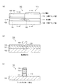
光導波路を伝搬する光強度を測定するには、一般的には、フォトダイオード部分の光吸収効率を高めるため、導波路とは異なる組成の半導体材料によって同一基板上にフォトダイオード領域を形成するため、導波路部分とは別々に結晶成長等の素子作製プロセスが必要となる(例えば、下記の非特許文献1参照)。ここで、上述した構成のリッジ型スラブ導波路と同一基板上にフォトダイオード部分を形成した従来の導波路型フォトダイオードについて図4(a),(b),(c)を用いて説明する。これら図に示すように、導波路型フォトダイオードは、導波路部分をなすリッジ型スラブ導波路100の下部クラッド層102(基板)と同一基板上にて、リッジ型スラブ導波路100に接して設けられたフォトダイオード部分110を備える。フォトダイオード部分110は、下部クラッド層102上に設けられた吸収層111と、吸収層111上に設けられた上部クラッド層113と、上部クラッド層113上に設けられた電極116(上部電極)とを備える。吸収層111は、リッジ型スラブ導波路100のコア層101と同一の厚さで且つ、このコア層101と異なる組成で形成される。フォトダイオード部分110の吸収層111における、導波路部分100の光が伝搬する領域105に対向する領域115にて、当該フォトダイオード部分110に入射した光を吸収している。
In order to measure the light intensity propagating in the optical waveguide, in general, in order to increase the light absorption efficiency of the photodiode portion, the photodiode region is formed on the same substrate with a semiconductor material having a composition different from that of the waveguide. In addition, an element manufacturing process such as crystal growth is required separately from the waveguide portion (see, for example, Non-Patent Document 1 below). Here, a conventional waveguide photodiode in which a photodiode portion is formed on the same substrate as the ridge slab waveguide having the above-described configuration will be described with reference to FIGS. 4 (a), 4 (b), and 4 (c). As shown in these figures, the waveguide photodiode is provided in contact with the
このように、異なる組成の半導体領域を同一基板上に形成するには、半導体エピタキシャル成長工程を複数回行い、結晶成長工程と所望の形状へ加工する工程とを繰り返す作製工程が必要となる。したがって、作製工程が複雑になり、また先に形成された半導体層は結晶成長の温度まで加熱される熱工程を再度経ることになり、特性の劣化や変性が生じることに注意する必要がある。 As described above, in order to form semiconductor regions having different compositions on the same substrate, it is necessary to perform a semiconductor epitaxial growth step a plurality of times and to repeat a crystal growth step and a step of processing into a desired shape. Therefore, it is necessary to note that the manufacturing process becomes complicated, and the previously formed semiconductor layer undergoes a thermal process that is heated to the temperature of crystal growth again, resulting in deterioration and modification of characteristics.
一方、半導体層に電界を印加することで、光吸収を増加させることが可能である。これはフランツケルディッシュ効果と呼ばれ、半導体に印加された電界によって、図5(b)に示すように、伝導帯151と価電子帯152のバンドが傾き、バンドギャップエネルギーより小さい光に対しても吸収を生じさせることが可能である。なお、電界印加なしの場合には、図5(a)に示すように、伝導帯141と価電子帯142のバンドは傾きがなく、バンドギャップエネルギーより小さい光に対して吸収が生じない状態となる。 On the other hand, light absorption can be increased by applying an electric field to the semiconductor layer. This is called the Franz-Keldish effect, and the band of the conduction band 151 and the valence band 152 is inclined by the electric field applied to the semiconductor as shown in FIG. Can also cause absorption. When no electric field is applied, as shown in FIG. 5A, the bands of the conduction band 141 and the valence band 142 are not inclined and no absorption occurs for light smaller than the band gap energy. Become.
電界印加によって十分な吸収係数増加を得るには、電界無印加の状態での半導体コア層のバンドギャップエネルギー波長を、光の波長に十分近接している組成の半導体によって形成する必要がある。この場合、温度のゆらぎ等によっても、電界無印加時でも吸収係数の変動が生じてしまうため、光を導波させる導波路部分においては伝搬損失が増加することになり、特性の劣化が生じてしまう。したがって、光導波路としては、ある程度バンドギャップエネルギー波長と光の波長を離すことで、吸収による伝搬損失を低減する必要があり、このような半導体組成で吸収層を形成したフォトダイオードでは、十分な光吸収を生じさせるために大きな電界を印加したり、十分な素子の長さとしたりする必要がある。 In order to obtain a sufficient increase in absorption coefficient by applying an electric field, it is necessary to form the band gap energy wavelength of the semiconductor core layer without applying an electric field from a semiconductor having a composition sufficiently close to the wavelength of light. In this case, the fluctuation of the absorption coefficient also occurs even when no electric field is applied due to temperature fluctuations, etc., so that the propagation loss increases in the waveguide portion that guides light, resulting in deterioration of characteristics. End up. Therefore, it is necessary for the optical waveguide to reduce the propagation loss due to absorption by separating the band gap energy wavelength and the light wavelength to some extent, and a photodiode having an absorption layer with such a semiconductor composition has sufficient light. In order to cause absorption, it is necessary to apply a large electric field or to have a sufficient element length.
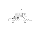
しかし、半導体の逆方向印加電界を大きくすると、局所的なリーク電流パスの形成や、強電界による半導体層の劣化といった、信頼性上の問題も考慮する必要が生じる。特に、側壁部分での強電界印加はブレークダウンや故障の原因となりやすいため、表面付近の電界強度を緩和するような構造が必要になる。例えば、強電界を印加した状態で動作するアバランシェフォトダイオードでは、傾斜メサ構造や、ガードリング構造が用いられる。例えば、図6に示すように、傾斜メサ構造の半導体デバイス120は、吸収層121、下部クラッド層122、上部クラッド層123、上部電極126を備え、吸収層121の幅が上部から下部側に向けて漸増して形成されている。つまり、吸収層121の側壁部121a,121bは傾斜状に形成されている。しかし、導波路型フォトダイオードでは、導波路幅によって表面電極幅が決まるため、十分な面積を形成することが困難であり、このような電界緩和のための形状を取り入れることは難しい。
However, when the electric field applied in the reverse direction of the semiconductor is increased, it is necessary to consider reliability problems such as formation of a local leakage current path and deterioration of the semiconductor layer due to a strong electric field. In particular, the application of a strong electric field at the side wall tends to cause breakdown and failure, so a structure that reduces the electric field strength near the surface is required. For example, in an avalanche photodiode that operates in a state where a strong electric field is applied, an inclined mesa structure or a guard ring structure is used. For example, as illustrated in FIG. 6, the
また、フォトダイオードとしての受光感度を大きくするためには、吸収領域を長くすることが必要であるが、集積デバイスでは素子の占有面積が大きくなり、素子設計上のデメリットとなってしまう。 Further, in order to increase the light receiving sensitivity as a photodiode, it is necessary to lengthen the absorption region. However, in the integrated device, the area occupied by the element increases, resulting in a demerit in element design.
以上のような観点から、これまでの導波路型デバイスによる光強度検出には、フォトダイオード部分をなす吸収領域の吸収層の半導体組成を、導波路部分をなす導波路領域のコア層の半導体組成と異なるもので構成する必要があった。 From the above viewpoint, the light intensity detection by the conventional waveguide type device can be performed by using the semiconductor composition of the absorption layer in the absorption region forming the photodiode portion and the semiconductor composition of the core layer in the waveguide region forming the waveguide portion. It was necessary to compose with something different.
光導波路として伝搬損失の少ないスラブ導波路構造をそのままフォトダイオードとして用いることができれば、組成の異なる半導体層構造を形成する必要がなく、これに要するコストの削減が可能となる。 If a slab waveguide structure with a small propagation loss can be used as an optical waveguide as it is as a photodiode, it is not necessary to form a semiconductor layer structure having a different composition, and the cost required for this can be reduced.
しかし、スラブ導波路構造のままでは、フォトダイオードを形成しても光の吸収係数が小さいため印加電界を大きくする必要があり、この場合導波路の側壁部分における高電界による故障等の信頼性上の問題が懸念される。また、光吸収による電流を十分に得る為には、吸収領域となる導波路フォトダイオード部分を長くする必要があり、これは集積デバイス内でのフォトダイオードの配置の自由度に制約を生じさせ、またデバイスの小型化を図る上で課題となる。 However, with the slab waveguide structure, it is necessary to increase the applied electric field because the light absorption coefficient is small even if a photodiode is formed. In this case, in view of reliability such as failure due to a high electric field in the sidewall portion of the waveguide Is concerned about the problem. In addition, in order to obtain a sufficient current due to light absorption, it is necessary to lengthen the waveguide photodiode portion that becomes the absorption region, which causes restrictions on the degree of freedom of the arrangement of the photodiode in the integrated device, In addition, it becomes a problem in miniaturization of the device.
以上のことから、本発明は上述したような課題を解決するために為されたものであって、低コストで高信頼性を有し、簡易に安定な光モニタ機能を発現し、小型である半導体受光装置を提供することを目的としている。 In view of the above, the present invention has been made to solve the above-described problems, has low cost and high reliability, easily expresses a stable light monitoring function, and is small in size. An object of the present invention is to provide a semiconductor light receiving device.
上述した課題を解決する本発明に係る半導体受光装置は、光が導波するリッジ型スラブ導波路領域に接続し、且つ前記リッジ型スラブ導波路領域と同一基板上に設けられ、入射した光を吸収するフォトダイオード領域を備える半導体受光装置であって、前記フォトダイオード領域が前記リッジ型半導体スラブ導波路と同じ半導体組成で形成された層構造をなすと共に、当該フォトダイオード領域の上部クラッド層の上部に設けられた上部電極を備え、前記フォトダイオード領域のコア層が、前記入射した光が内部を導波し周回しつつ吸収する周回形状の吸収層をなし、前記上部電極の端部が前記吸収層の端部よりも内側に配置されることを特徴とする。
前記リッジ型スラブ導波路領域は、コア層と、下部クラッド層、上部クラッド層を備え、前記上部クラッド層をリッジ型構造とし、前記コア層における前記上部クラッド層のリッジ部直下の領域が光を導波する領域をなしている。
A semiconductor light-receiving device according to the present invention that solves the above-described problems is connected to a ridge-type slab waveguide region where light is guided, and is provided on the same substrate as the ridge-type slab waveguide region. A semiconductor light receiving device including a photodiode region to absorb, wherein the photodiode region has a layer structure formed of the same semiconductor composition as that of the ridge-type semiconductor slab waveguide, and an upper portion of an upper cladding layer of the photodiode region. An upper electrode provided on the photodiode region, wherein the core layer of the photodiode region forms a circular absorption layer in which the incident light is absorbed while being guided around, and an end portion of the upper electrode is the absorption It is characterized by being arranged inside the end of the layer.
The ridge slab waveguide region includes a core layer, a lower clad layer, and an upper clad layer. The upper clad layer has a ridge structure, and a region immediately below the ridge portion of the upper clad layer in the core layer emits light. A wave guiding region is formed.
上述した課題を解決する本発明に係る半導体受光装置は、前述した発明に係る半導体受光装置であって、前記吸収層が、円形状または多角形状に形成されていることを特徴とする。 A semiconductor light-receiving device according to the present invention that solves the above-described problems is the semiconductor light-receiving device according to the above-described invention, wherein the absorption layer is formed in a circular shape or a polygonal shape.
上述した課題を解決する本発明に係る半導体受光装置は、前述した発明に係る半導体受光装置であって、前記吸収層が、前記リッジ型スラブ導波路領域における前記光が導波する部分よりも幅広であることを特徴とする。 A semiconductor light-receiving device according to the present invention that solves the above-described problems is the semiconductor light-receiving device according to the above-described invention, wherein the absorption layer is wider than a portion of the ridge-type slab waveguide region where the light is guided. It is characterized by being.
上述した課題を解決する本発明に係る半導体受光装置は、前述した発明に係る半導体受光装置であって、前記吸収層と前記半導体スラブ導波路領域が、当該吸収層の接線方向にて接続することを特徴とする。 A semiconductor light-receiving device according to the present invention that solves the above-described problems is the semiconductor light-receiving device according to the above-described invention, wherein the absorption layer and the semiconductor slab waveguide region are connected in a tangential direction of the absorption layer. It is characterized by.
本発明に係る半導体受光装置によれば、フォトダイオード領域がリッジ型スラブ導波路領域と同じ半導体組成で形成された層構造をなすことにより、リッジ型スラブ導波路領域とフォトダイオード領域の層構造を同じ結晶成長工程で作製することができる。これにより、作製工程が簡易になり、低コストで高信頼性を実現できる。フォトダイオード領域のコア層が、入射した光が内部を導波し周回しつつ吸収する周回形状の吸収層をなすことにより、吸収層の小型化、つまり半導体受光装置の小型化を図ることができる。上部電極の端部が吸収層の端部よりも内側に配置されることにより、局所的なリーク電流のパスの形成や、強電界による半導体層の劣化を生じることなく、簡易に安定な光モニタ機能を発現することができる。 According to the semiconductor light receiving device of the present invention, the layer structure of the ridge slab waveguide region and the photodiode region is formed by forming a layer structure in which the photodiode region is formed with the same semiconductor composition as the ridge slab waveguide region. The same crystal growth process can be used. Thereby, the manufacturing process is simplified, and high reliability can be realized at low cost. The core layer in the photodiode region forms a circular absorption layer in which incident light is guided around the inside and absorbed while rotating, so that the absorption layer can be downsized, that is, the semiconductor light receiving device can be downsized. . By arranging the end of the upper electrode on the inner side of the end of the absorption layer, it is possible to easily and stably monitor the light without forming a local leakage current path or causing deterioration of the semiconductor layer due to a strong electric field. Function can be expressed.
以下、本発明に係る半導体受光装置を実施するための一つの形態について説明する。 Hereinafter, one embodiment for implementing a semiconductor light receiving device according to the present invention will be described.
本実施形態に係る半導体受光装置をなすフォトダイオードは、光が導波する半導体スラブ導波路と同じ半導体組成で形成された層構造をなしている。つまり、フォトダイオードの吸収層(コア層)として、半導体スラブ導波路(光導波路)のコア層をそのまま用いることを特徴とする。これにより、フォトダイオードにおける光の吸収層を別組成の半導体で形成するための再成長工程や選択成長工程を省くことができ、これによる作製コストの低減や、再成長工程時の熱履歴の影響をなくすことが可能になる。 The photodiode constituting the semiconductor light receiving device according to the present embodiment has a layer structure formed of the same semiconductor composition as the semiconductor slab waveguide through which light is guided. In other words, the core layer of the semiconductor slab waveguide (optical waveguide) is used as it is as the absorption layer (core layer) of the photodiode. As a result, the regrowth process and selective growth process for forming the light absorption layer of the photodiode with a semiconductor of another composition can be omitted, thereby reducing the manufacturing cost and the influence of the thermal history during the regrowth process. Can be eliminated.
このような半導体スラブ導波路のコア層の組成からなる半導体層をフォトダイオードの吸収層(コア層)として用いる場合、吸収係数が小さいため、十分な長さ(大きさ)が必要となる。これを直線状の導波路構造とすると、フォトダイオード部分の占める面積が従来のフォトダイオード部分と比べて大きくなってしまうため、スラブ導波路構造で、円形あるいは内角が全反射角となる多角形の形状とする。このようなフォトダイオード部分に入射した光は、円形導波路の内周を周回し、あるいは、全反射角を持つ側壁部(側壁面)で反射しながら、フォトダイオードを形成する周回導波路を周回し続ける。これによって、実効的に十分な長さを得ることが可能となり、入射した光は吸収層に吸収されて電気に変換することが可能となる。このように周回導波路型をなすフォトダイオード部分の吸収層で入射した光を吸収することができるため、光の伝搬方向に対して直線状をなし導波路のコア層と同一の半導体組成でフォトダイオード部分の吸収層を形成した場合と比べて、約10分の1程度の大きさにすることが可能となる。 When a semiconductor layer having such a composition of the core layer of the semiconductor slab waveguide is used as the absorption layer (core layer) of the photodiode, the absorption coefficient is small, so that a sufficient length (size) is required. If this is a straight waveguide structure, the area occupied by the photodiode portion will be larger than that of the conventional photodiode portion. Therefore, in the slab waveguide structure, a polygon or a polygon whose interior angle is the total reflection angle is used. Shape. The light incident on the photodiode part circulates around the inner circumference of the circular waveguide or circulates around the circular waveguide forming the photodiode while being reflected by the side wall (side wall surface) having a total reflection angle. Keep doing. This makes it possible to obtain a sufficient length effectively, and incident light can be absorbed by the absorption layer and converted into electricity. In this way, the incident light can be absorbed by the absorption layer of the photodiode portion of the circular waveguide type, so that it is linear with respect to the light propagation direction and has the same semiconductor composition as the core layer of the waveguide. Compared with the case where the absorption layer of the diode portion is formed, the size can be reduced to about 1/10.
また、この領域へは印加電界を大きくする必要がある。従来の導波路型フォトダイオードでは、導波路構造を維持するために伝搬方向に沿って細長い形状となっており、ここに強電界を印加すると、導波路側壁部分に電界が集中してしまうため、表面のリーク電流増加や電気的故障といった信頼性上の問題が生じていた。ここで、吸収層を周回導波路構造とすることで、導波路中央部分には十分な電極形成のための面積を確保することが可能となる。したがって、導波路の端面付近まで電極を形成する必要がなくなり、端面から十分離れた中央部分に電極を形成することで、端面付近への電界集中を緩和することが可能になる。 Further, it is necessary to increase the applied electric field to this region. The conventional waveguide type photodiode has an elongated shape along the propagation direction in order to maintain the waveguide structure. When a strong electric field is applied to the photodiode, the electric field concentrates on the side wall portion of the waveguide. Reliability problems such as increased leakage current on the surface and electrical failure have occurred. Here, when the absorption layer has a circular waveguide structure, a sufficient area for electrode formation can be secured in the central portion of the waveguide. Therefore, it is not necessary to form an electrode up to the vicinity of the end face of the waveguide, and by forming the electrode in the central portion sufficiently away from the end face, it is possible to alleviate electric field concentration near the end face.
このようにして、高信頼性を保持したまま、スラブ導波路構造のフォトダイオード部分に、比較的大きな電界を印加することが可能となる。 In this way, it is possible to apply a relatively large electric field to the photodiode portion of the slab waveguide structure while maintaining high reliability.
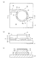
本発明の第1の実施例に係る半導体受光装置について図1(a)および図1(b)ならびに図1(c)を参照して説明する。なお、図1(a)においては、半導体スラブ導波路領域におけるリッジ部を省略して図示している。 A semiconductor light receiving device according to a first embodiment of the present invention will be described with reference to FIGS. 1 (a), 1 (b) and 1 (c). In FIG. 1A, the ridge portion in the semiconductor slab waveguide region is omitted.
本実施例に係る半導体受光装置をなす半導体デバイスは、図1(a),(b),(c)に示すように、光が導波するリッジ型スラブ導波路領域30に接続し、且つ、リッジ型スラブ導波路領域30と同一の基板である下部クラッド層32上に設けられ、入射した光を吸収するフォトダイオード領域10を備える。
As shown in FIGS. 1A, 1B, and 1C, the semiconductor device constituting the semiconductor light receiving device according to the present embodiment is connected to a ridge
リッジ型スラブ導波路領域30は、コア層31と、コア層31の下部および上部のそれぞれに設けられた下部クラッド層32および上部クラッド層33とを備え、上部クラッド層33が所定幅を持つリッジ型構造をとっている。すなわち、上部クラッド層33には、所定幅を持つリッジ部34が形成されている。このような構成のリッジ型スラブ導波路領域30においては、光はコア層31におけるリッジ部34直下の領域を導波する。
The ridge-type
フォトダイオード領域10は、リッジ型スラブ導波路領域30と同じ半導体組成で形成された層構造で構成される。フォトダイオード領域10は、下部クラッド層32上に設けられた吸収層(コア層)11と、吸収層11上に設けられた上部クラッド層13とを備え、上部クラッド層13が所定幅を持つリッジ型構造をとっている。上部クラッド層13には、所定幅を持つリッジ部14が形成される。リッジ部14の上部には、光吸収電流を取り出す上部電極(金属電極)16が形成される。つまり、上部クラッド層13と上部クラッド層33、吸収層11とコア層31がそれぞれ同じ半導体組成で形成される。吸収層11では、入射した光が導波しつつ当該光を吸収している。また、電界を印加するための電極のうち、層構造下部には例えばn型ドーピングの伝導型半導体層を全面に形成して、吸収層11とは別の位置に、すなわち、フォトダイオード領域10の下部クラッド層32の下部における上部電極16の直下から離れた箇所に下部電極(金属パッド)17が形成される。
The
吸収層11および上部クラッド層13は円柱体状に形成されており、吸収層11の周壁部11aおよび上部クラッド層13の周壁部13aは平面にて円形を成している。上部電極16はリッジ部14と同じ円形状に形成されている。つまり、上部電極16は吸収層11の中央部に配置され、上部電極16の周壁部(端部)16aは吸収層11の側壁部11aよりも内側にずらした位置に配置される。これにより、吸収層11の周壁部11a近傍での電界強度を低減し、電界印加時のリークパス形成や電界集中による破壊を防止することができる。
The
上述した構成の半導体受光装置では、リッジ型スラブ導波路領域30を導波した光51は、当該リッジ型スラブ導波路領域30からリッジ型スラブ導波路領域30と同一の層構造からなるフォトダイオード領域10へ入射することになる。ここで、フォトダイオード領域10へ入射した光52は、円形に加工された導波路部分をなす吸収層11の内周を伝搬しながら、吸収層11の円形形状を周回することになる。導波路部分をなす吸収層11の側壁部11aでは、半導体と空気との屈折率の違いによって、伝搬する光52は吸収層11の外側に放射されずに周回することになる。つまり、吸収層11は周回形状を成している。
In the semiconductor light receiving device configured as described above, the light 51 guided through the ridge
上述したように、リッジ部14上に上部電極16を形成することで、周回形状の吸収層11の上下に電界を印加することができる。つまり、上部電極16および下部電極17にバイアス電圧を印加することで、吸収層11(コア層)に電界を印加することができる。上下に印加された電界によって、半導体の吸収係数が大きくなり、光は半導体に吸収され、電子・正孔対を発生し、この発生したキャリアは電界によって電極へ運ばれ、電流として取り出される。
As described above, by forming the
よって、吸収層11を周回する光52は徐々に吸収されて、電気信号に変換されるため、そのまま光として外部に透過されることはない。
Therefore, the light 52 that circulates around the
以上説明したように、本実施例に係る半導体受光装置によれば、フォトダイオード領域10の吸収層11が、光が周回する周回形状をなすことにより、リッジ型スラブ導波路領域と同じ層構造であって吸収層を直線状に設けたフォトダイオードと比べて、10分の1以下の大きさにすることができる。すなわち、半導体受光装置の小型化を図ることができる。さらに、フォトダイオード領域10を小型に形成することが可能であるため、集積デバイスの設計自由度の向上にも寄与することができる。
As described above, according to the semiconductor light receiving device according to the present embodiment, the
また、フォトダイオード領域10がリッジ型スラブ導波路領域30と同じ半導体組成で形成される層構造をなすことにより、リッジ型スラブ導波路領域30とフォトダイオード領域10の層構造を同じ結晶成長工程で作製することができる。
Further, by forming a layer structure in which the
したがって、本実施例に係る半導体受光装置を用いることで、従来の半導体導波路型フォトダイオードに比べて、フォトダイオード領域のための光吸収層形成に伴う再成長工程や選択成長工程を用いることが必要なく、またこれらによる熱履歴の影響を考慮する必要がないため、低コストで高信頼性を有し、簡易に安定な光モニタ機能を半導体導波路デバイスに内蔵することができる。 Therefore, by using the semiconductor light receiving device according to the present embodiment, it is possible to use the regrowth process and the selective growth process associated with the formation of the light absorption layer for the photodiode region as compared with the conventional semiconductor waveguide photodiode. Since it is not necessary and it is not necessary to consider the influence of the thermal history due to these, it is possible to easily incorporate a stable and stable optical monitor function into a semiconductor waveguide device at a low cost.
吸収層11がリッジ型スラブ導波路領域30における光が導波する部分よりも幅広であることで、リッジ型スラブ導波路領域30からフォトダイオード領域10に光が入射したときに、光の強度が高い部分(光の中心部分)が吸収層11内にて周回方向へ伝搬し、光の強度が低い部分(光の外側部分)が吸収層11内にて広がるが当該吸収層11内にて周方向へ伝搬する。これにより、フォトダイオード領域10内へ入射した光52がリッジ型スラブ導波路領域30へ出射してしまう可能性は低減される。
Since the
吸収層11とリッジ型スラブ導波路領域30が吸収層11の平面における接線方向にて接続することにより、フォトダイオード領域10に入射した光52がフォトダイオード領域10内にて周回することになる。これにより、フォトダイオード領域10内へ入射した光52がリッジ型スラブ導波路領域30へ出射してしまう可能性は低減される。
When the
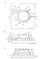
本発明の第2の実施例に係る半導体受光装置について、図2(a)および図2(b)ならびに図2(c)を参照して説明する。なお、図2(a)においては、半導体スラブ導波路領域におけるリッジ部を省略して図示している。
本実施例に係る半導体受光装置は、上述した第1の実施例に係る半導体受光装置が備えるフォトダイオード領域の形態を変更したものであって、それ以外は上述した第1の実施例に係る半導体受光装置と同じ構成であり、作用効果も同じである。したがって、ここでは、第1の実施例に係る半導体受光装置と異なる部分についてのみ説明する。なお、本実施例では、第1の実施例に係る半導体受光装置と同じ構成には同一の符号を付記している。
A semiconductor light receiving device according to a second embodiment of the present invention will be described with reference to FIGS. 2 (a), 2 (b) and 2 (c). In FIG. 2A, the ridge portion in the semiconductor slab waveguide region is omitted.
The semiconductor light-receiving device according to this example is obtained by changing the form of the photodiode region included in the semiconductor light-receiving device according to the above-described first example, and other than that, the semiconductor according to the above-described first example The configuration is the same as that of the light receiving device, and the operational effects are also the same. Therefore, only the parts different from the semiconductor light receiving device according to the first embodiment will be described here. In the present embodiment, the same components as those in the semiconductor light receiving device according to the first embodiment are denoted by the same reference numerals.
本実施例に係る半導体受光装置をなす半導体デバイスは、図2(a),(b),(c)に示すように、光が導波するリッジ型スラブ導波路領域30に接続し、且つ、リッジ型スラブ導波路領域30と同一の基板である下部クラッド層32上に設けられ、入射した光を吸収するフォトダイオード領域20を備える。
As shown in FIGS. 2A, 2B, and 2C, the semiconductor device constituting the semiconductor light receiving device according to this embodiment is connected to a ridge
フォトダイオード領域20は、リッジ型スラブ導波路領域30と同じ半導体組成で形成された層構造で構成される。フォトダイオード領域20は、下部クラッド層32上に設けられた吸収層(コア層)21と、吸収層21上に設けられた上部クラッド層23とを備え、上部クラッド層23が所定幅を持つリッジ型構造をとっている。上部クラッド層23には、所定幅を持つリッジ部24が形成される。リッジ部24の上部には、光吸収電流を取り出す上部電極(金属電極)26が形成される。つまり、上部クラッド層23と上部クラッド層33、吸収層21とコア層31がそれぞれ同じ半導体組成で形成される。吸収層21では、入射した光が導波しつつ当該光を吸収している。また、電界を印加するための電極のうち、層構造下部には例えばn型ドーピングの伝導型半導体層を全面に形成して、吸収層21とは別の位置に、すなわち、フォトダイオード領域20の下部クラッド32の下部における上部電極26の直下から離れた箇所に下部電極(金属パッド)27が形成される。
The
吸収層21および上部クラッド層23は正八角柱体状に形成されており、吸収層21の周壁部21aおよび上部クラッド層23の周壁部23aは平面にて正八角形状を成している。上部電極26はリッジ部24と同じ正八角形状に形成されている。つまり、上部電極26は吸収層21の中央部に配置され、上部電極26の周壁部(端部)26aは吸収層21の側壁部21aよりも内側にずらした位置に配置される。これにより、吸収層21の周壁部21a近傍での電界強度を低減し、電界印加時のリークパス形成や電界集中による破壊を防止することができる。
The absorbing
上述した構成の半導体受光装置では、リッジ型スラブ導波路領域30を導波した光61は、当該リッジ型スラブ導波路領域30からリッジ型スラブ導波路領域30と同一層構造からなるフォトダイオード領域20へ入射することになる。ここで、フォトダイオード領域20へ入射した光62は、正八角形に加工された導波路部分をなす吸収層21の内周を全反射しながら伝搬し、吸収層21の正八角形状を周回することになる。導波路部分をなす吸収層21の側壁部21aでは、半導体と空気との屈折率の違いによって、伝搬する光62は吸収層21の外側に放射されずに周回することになる。つまり、吸収層21は周回形状を成している。
In the semiconductor light receiving device having the above-described configuration, the light 61 guided through the ridge
上述したように、リッジ部24上に上部電極26を形成することで、周回形状の吸収層21の上下に電界を印加することができる。つまり、上部電極26および下部電極27にバイアス電圧を印加することで、吸収層21(コア層)に電界を印加することができる。上下に印加された電界によって、半導体の吸収係数が大きくなり、光は半導体に吸収され、電子・正孔対を発生し、この発生したキャリアは電界によって電極へ運ばれ、電流として取り出される。
As described above, by forming the
よって、吸収層21を周回する光62は徐々に吸収され、電気信号に変換されるため、そのまま光として外部に透過されることはない。
Therefore, since the light 62 circulating around the
以上説明したように、本実施例に係る半導体受光装置によれば、フォトダイオード領域20の吸収層21が、光が周回する周回形状をなすことにより、上述した第1の実施例の場合と同様、リッジ型スラブ導波路領域と同じ層構造であって吸収層を直線状に設けたフォトダイオードと比べて、10分の1以下の大きさにすることができる。すなわち、半導体受光装置の小型化を図ることができる。さらに、フォトダイオード領域20は小型に形成することが可能であるため、集積デバイスの設計自由度の向上にも寄与することができる。
As described above, according to the semiconductor light receiving device according to the present embodiment, the
また、フォトダイオード領域20がリッジ型スラブ導波路領域30と同じ半導体組成で形成される層構造をなすことにより、リッジ型スラブ導波路領域30とフォトダイオード領域20の層構造を同じ結晶成長工程で作製することができる。
Further, by forming a layer structure in which the
したがって、本実施例に係る半導体受光装置を用いることで、従来の半導体導波路型フォトダイオードに比べて、フォトダイオード領域のための光吸収層形成に伴う再成長工程や選択成長工程を用いることが必要なく、またこれらによる熱履歴の影響を考慮する必要がないため、低コストで高信頼性を有し、簡易に安定な光モニタ機能を半導体導波路デバイスに内蔵することができる。 Therefore, by using the semiconductor light receiving device according to the present embodiment, it is possible to use the regrowth process and the selective growth process associated with the formation of the light absorption layer for the photodiode region as compared with the conventional semiconductor waveguide photodiode. Since it is not necessary and it is not necessary to consider the influence of the thermal history due to these, it is possible to easily incorporate a stable and stable optical monitor function into a semiconductor waveguide device at a low cost.
吸収層21がリッジ型スラブ導波路領域30における光が導波する部分よりも幅広であることで、リッジ型スラブ導波路領域30からフォトダイオード領域20に光が入射したときに、光の強度が高い部分(光の中心部分)が吸収層21内にて周回方向へ伝搬し、光の強度が低い部分(光の外側部分)が吸収層21内にて広がるが当該吸収層21内にて周方向へ伝搬する。これにより、フォトダイオード領域20内へ入射した光62がリッジ型スラブ導波路領域30へ出射してしまう可能性は低減される。
Since the
吸収層21とリッジ型スラブ導波路領域30が吸収層21の平面における接線方向にて接続することにより、半導体スラブ導波路領域30の延在方向とその正面をなす吸収層21の側壁部21aが鈍角をなし、フォトダイオード領域20に入射した光62が吸収層21の側壁部21aで反射したときに、スラブ導波路領域30へは伝搬せずに吸収層21内を周回することになる。これにより、フォトダイオード領域20内へ入射した光62がリッジ型スラブ導波路領域30へ出射してしまう可能性は低減される。
The
なお、上記では、平面にて円形をなす吸収層11を備える半導体受光装置、平面にて正八角形状をなす吸収層21を備える半導体受光装置について説明したが、吸収層に入射した光が周回する形状であれば良く、例えば、平面にて楕円形状をなす吸収層を備える半導体受光装置、平面にて正八角形状以外の多角形状をなす吸収層を備える半導体受光装置とすることも可能である。なお、吸収層が四角形状である場合には、リッジ型スラブ導波路領域における光が伝搬する部分よりも吸収層を平面にて幅広とし吸収層内に入射した光が周囲に拡がるようにしたり、リッジ型スラブ導波路領域の延在方向と当該リッジ型半導体スラブ導波路の延在方向に対向する吸収層の側壁部とで鋭角または鈍角をなす様にフォトダイオード領域を配置したりすれば良い。
In the above description, the semiconductor light-receiving device including the
上記では、リッジ型スラブ導波路領域30における光51が伝搬する部分よりも幅広に形成されたフォトダイオード領域10の吸収層11を備える半導体受光装置、リッジ型スラブ導波路領域30における光61が伝搬する部分よりも幅広に形成されたフォトダイオード領域20を備える半導体受光装置について説明したが、リッジ型スラブ導波路領域における光が伝搬する部分よりも幅狭に形成されたフォトダイオード領域の吸収層を備える半導体受光装置とすることも可能である。つまり、フォトダイオード領域の吸収層は、入射した光が内部で周回することができる形状であれば良い。
In the above, the semiconductor light receiving device including the
上記では、リッジ型スラブ導波路領域30とフォトダイオード領域10とが吸収層11の平面における接線方向にて接続する半導体受光装置、リッジ型スラブ導波路領域30とフォトダイオード領域20とが吸収層21の平面における接線方向にて接続する半導体受光装置について説明したが、リッジ型スラブ導波路領域とフォトダイオード領域とは、吸収層の平面における接線方向に限らず他の箇所で接続する半導体受光装置とすることも可能である。
In the above, the semiconductor light receiving device in which the ridge
本発明は半導体受光装置に関するものであり、低コストで高信頼性を有し、簡易に安定な光モニタ機能を発現し、小型化を図ることができるので、光通信産業などにおいて、極めて有益に利用することができる。 The present invention relates to a semiconductor light receiving device, which is low-cost, highly reliable, easily expresses a stable optical monitoring function, and can be downsized, which is extremely useful in the optical communication industry and the like. Can be used.
10 フォトダイオード領域
11 吸収層
13 上部クラッド層
14 リッジ部
16 上部電極
17 下部電極
20 フォトダイオード領域
21 吸収層
23 上部クラッド層
24 リッジ部
26 上部電極
27 下部電極
30 リッジ型スラブ導波路領域
31 コア層
32 下部クラッド層
33 上部クラッド層
34 リッジ部
51 導波路領域を導波する光
52 フォトダイオード領域を伝搬する光
61 導波路領域を導波する光
62 フォトダイオード領域を伝搬する光
DESCRIPTION OF
Claims (4)
前記フォトダイオード領域が前記リッジ型スラブ導波路領域と同じ半導体組成で形成された層構造をなすと共に、当該フォトダイオード領域の上部クラッド層の上部に設けられた上部電極を備え、
前記フォトダイオード領域のコア層が、前記入射した光が内部を導波し周回しつつ吸収する周回形状の吸収層をなし、
前記上部電極の端部が前記吸収層の端部よりも内側に配置される
ことを特徴とする半導体受光装置。 A semiconductor light receiving device that includes a photodiode region that is connected to a ridge slab waveguide region where light is guided and is provided on the same substrate as the ridge slab waveguide region and absorbs incident light,
The photodiode region has a layer structure formed of the same semiconductor composition as the ridge-type slab waveguide region, and includes an upper electrode provided on the upper cladding layer of the photodiode region,
The core layer of the photodiode region forms a circular absorption layer in which the incident light is absorbed while being guided around the inside,
The semiconductor light-receiving device, wherein an end portion of the upper electrode is disposed inside an end portion of the absorption layer.
前記吸収層が、円形状または多角形状に形成されている
ことを特徴とする半導体受光装置。 The semiconductor light-receiving device according to claim 1,
The semiconductor light-receiving device, wherein the absorption layer is formed in a circular shape or a polygonal shape.
前記吸収層は、前記リッジ型スラブ導波路領域における前記光が導波する部分よりも幅広である
ことを特徴とする半導体受光装置。 The semiconductor light-receiving device according to claim 1 or 2,
The semiconductor light-receiving device, wherein the absorption layer is wider than a portion where the light is guided in the ridge-type slab waveguide region.
前記吸収層と前記リッジ型スラブ導波路領域は、当該吸収層の接線方向にて接続する
ことを特徴とする半導体受光装置。 The semiconductor light-receiving device according to claim 3,
The semiconductor light receiving device, wherein the absorption layer and the ridge slab waveguide region are connected in a tangential direction of the absorption layer.
Priority Applications (1)
| Application Number | Priority Date | Filing Date | Title |
|---|---|---|---|
| JP2011117578A JP2012248587A (en) | 2011-05-26 | 2011-05-26 | Semiconductor light-receiving device |
Applications Claiming Priority (1)
| Application Number | Priority Date | Filing Date | Title |
|---|---|---|---|
| JP2011117578A JP2012248587A (en) | 2011-05-26 | 2011-05-26 | Semiconductor light-receiving device |
Publications (1)
| Publication Number | Publication Date |
|---|---|
| JP2012248587A true JP2012248587A (en) | 2012-12-13 |
Family
ID=47468806
Family Applications (1)
| Application Number | Title | Priority Date | Filing Date |
|---|---|---|---|
| JP2011117578A Pending JP2012248587A (en) | 2011-05-26 | 2011-05-26 | Semiconductor light-receiving device |
Country Status (1)
| Country | Link |
|---|---|
| JP (1) | JP2012248587A (en) |
Cited By (4)
| Publication number | Priority date | Publication date | Assignee | Title |
|---|---|---|---|---|
| JP2014203895A (en) * | 2013-04-02 | 2014-10-27 | 日本電信電話株式会社 | Photodiode |
| JP2016063102A (en) * | 2014-09-19 | 2016-04-25 | 株式会社東芝 | Semiconductor light-receiving element |
| CN110325900A (en) * | 2016-12-02 | 2019-10-11 | 洛克利光子有限公司 | Waveguide photoelectric device |
| CN111697087A (en) * | 2020-06-22 | 2020-09-22 | 三明学院 | Novel photoelectric micro-ring and novel photoelectric detector |
Citations (4)
| Publication number | Priority date | Publication date | Assignee | Title |
|---|---|---|---|---|
| JPH06109935A (en) * | 1992-09-29 | 1994-04-22 | Fujitsu Ltd | Wavelength-selective photodetecting device |
| JPH0818026A (en) * | 1994-06-29 | 1996-01-19 | Nec Corp | Semiconductor light waveguide path integration type light reception element |
| JPH1012912A (en) * | 1996-06-20 | 1998-01-16 | Nec Corp | Waveguide-type semiconductor light-receiving element |
| JP2003534650A (en) * | 2000-05-20 | 2003-11-18 | キネティック リミテッド | Horizontal access semiconductor photodiode |
-
2011
- 2011-05-26 JP JP2011117578A patent/JP2012248587A/en active Pending
Patent Citations (4)
| Publication number | Priority date | Publication date | Assignee | Title |
|---|---|---|---|---|
| JPH06109935A (en) * | 1992-09-29 | 1994-04-22 | Fujitsu Ltd | Wavelength-selective photodetecting device |
| JPH0818026A (en) * | 1994-06-29 | 1996-01-19 | Nec Corp | Semiconductor light waveguide path integration type light reception element |
| JPH1012912A (en) * | 1996-06-20 | 1998-01-16 | Nec Corp | Waveguide-type semiconductor light-receiving element |
| JP2003534650A (en) * | 2000-05-20 | 2003-11-18 | キネティック リミテッド | Horizontal access semiconductor photodiode |
Cited By (6)
| Publication number | Priority date | Publication date | Assignee | Title |
|---|---|---|---|---|
| JP2014203895A (en) * | 2013-04-02 | 2014-10-27 | 日本電信電話株式会社 | Photodiode |
| JP2016063102A (en) * | 2014-09-19 | 2016-04-25 | 株式会社東芝 | Semiconductor light-receiving element |
| CN110325900A (en) * | 2016-12-02 | 2019-10-11 | 洛克利光子有限公司 | Waveguide photoelectric device |
| CN110325900B (en) * | 2016-12-02 | 2023-11-17 | 洛克利光子有限公司 | Waveguide optoelectronic device |
| CN111697087A (en) * | 2020-06-22 | 2020-09-22 | 三明学院 | Novel photoelectric micro-ring and novel photoelectric detector |
| CN111697087B (en) * | 2020-06-22 | 2022-04-05 | 三明学院 | Photoelectric micro-ring and photoelectric detector |
Similar Documents
| Publication | Publication Date | Title |
|---|---|---|
| CN107532967B (en) | System for testing performance of optical device and method for testing optical device | |
| US9008473B2 (en) | Optical transmission-reception system and light-receiving unit | |
| US9229179B2 (en) | Integrated optoelectronic module | |
| US7751655B2 (en) | Micro-ring optical detector/modulator | |
| WO2008128202A2 (en) | Design of cmos integrated germanium photodiodes | |
| JP5262293B2 (en) | Optical semiconductor device | |
| JPH05198829A (en) | Optoelectronic device with overall optical guide and photodetector | |
| JP2014160881A (en) | Surface plasmon polariton photo-detector coupled to waveguide | |
| JP2018026478A (en) | Light-emitting element, light-emitting element array, and optical transmission device | |
| JP2012248587A (en) | Semiconductor light-receiving device | |
| JPWO2019111401A1 (en) | Semiconductor optical device | |
| JP5513659B1 (en) | Photonic crystal photodetector | |
| JP2014039021A (en) | Semiconductor optical element | |
| JP2007013065A (en) | Near infrared photodetection element | |
| US8855163B2 (en) | Optical semiconductor device | |
| JP2009117499A (en) | Photodetector | |
| US20120280347A1 (en) | Waveguide photo-detector | |
| US20120027340A1 (en) | Semiconductor Through-Wafer Electrical Signal-Carrying Waveguide | |
| JP2014530388A (en) | Resonator with reduced loss | |
| JP7125822B2 (en) | Optical semiconductor device and optical transmission device | |
| JP5759414B2 (en) | Semiconductor optical waveguide device | |
| JP4158197B2 (en) | Light receiving element | |
| US7071524B2 (en) | Semiconductor light receiving device for repeatedly propagating incident light in light absorption layer and method for manufacturing the same | |
| US20050053349A1 (en) | Waveguide photodetector | |
| JP2011165848A (en) | Surface incident type photodiode |
Legal Events
| Date | Code | Title | Description |
|---|---|---|---|
| RD01 | Notification of change of attorney |
Free format text: JAPANESE INTERMEDIATE CODE: A7426 Effective date: 20130304 |
|
| A621 | Written request for application examination |
Free format text: JAPANESE INTERMEDIATE CODE: A621 Effective date: 20130827 |
|
| A977 | Report on retrieval |
Free format text: JAPANESE INTERMEDIATE CODE: A971007 Effective date: 20140812 |
|
| A131 | Notification of reasons for refusal |
Free format text: JAPANESE INTERMEDIATE CODE: A131 Effective date: 20140819 |
|
| A521 | Request for written amendment filed |
Free format text: JAPANESE INTERMEDIATE CODE: A523 Effective date: 20141010 |
|
| A131 | Notification of reasons for refusal |
Free format text: JAPANESE INTERMEDIATE CODE: A131 Effective date: 20150331 |
|
| A02 | Decision of refusal |
Free format text: JAPANESE INTERMEDIATE CODE: A02 Effective date: 20150721 |