JP2012247663A - Liquid crystal device, projection type display device, and electronic appliance - Google Patents

Liquid crystal device, projection type display device, and electronic appliance Download PDF

Info

Publication number
JP2012247663A
JP2012247663A JP2011120049A JP2011120049A JP2012247663A JP 2012247663 A JP2012247663 A JP 2012247663A JP 2011120049 A JP2011120049 A JP 2011120049A JP 2011120049 A JP2011120049 A JP 2011120049A JP 2012247663 A JP2012247663 A JP 2012247663A
Authority
JP
Japan
Prior art keywords
electrode
liquid crystal
layer
crystal device
light
Prior art date
Legal status (The legal status is an assumption and is not a legal conclusion. Google has not performed a legal analysis and makes no representation as to the accuracy of the status listed.)
Withdrawn
Application number
JP2011120049A
Other languages
Japanese (ja)
Inventor
Takaaki Tanaka
孝昭 田中
Current Assignee (The listed assignees may be inaccurate. Google has not performed a legal analysis and makes no representation or warranty as to the accuracy of the list.)
Seiko Epson Corp
Original Assignee
Seiko Epson Corp
Priority date (The priority date is an assumption and is not a legal conclusion. Google has not performed a legal analysis and makes no representation as to the accuracy of the date listed.)
Filing date
Publication date
Application filed by Seiko Epson Corp filed Critical Seiko Epson Corp
Priority to JP2011120049A priority Critical patent/JP2012247663A/en
Publication of JP2012247663A publication Critical patent/JP2012247663A/en
Withdrawn legal-status Critical Current

Links

Images

Abstract

PROBLEM TO BE SOLVED: To provide a liquid crystal device in which deterioration of display quality due to aggregation of ionic impurities in an image display region can be prevented by neutralizing the ionic impurities into non-ionic impurities, and provide a projection type display device and an electronic appliance including the liquid crystal device.SOLUTION: A liquid crystal device 100 includes a first electrode 81 and a second electrode 82 which are in contact with a liquid crystal layer 50 in a peripheral region 10b of an element substrate 10 and a counter substrate 20. Different potentials are applied to the first electrode 81 and the second electrode 82. The first electrode 81 has a structure in which a first charge injection layer 812 is stacked on a first conductive layer 811, and the second electrode 82 has a structure in which a second charge injection layer 822 is stacked on a second conductive layer 821. Thus, ionic impurities exchange charges with the first electrode 81 or the second electrode 82 to become non-ionic impurities.

Description

本発明は、一対の基板間に液晶層が保持された液晶装置、当該液晶装置をライトバルブとして用いた投射型表示装置、および電子機器に関するものである。   The present invention relates to a liquid crystal device in which a liquid crystal layer is held between a pair of substrates, a projection display device using the liquid crystal device as a light valve, and an electronic apparatus.

液晶装置は、一方面側に複数の画素電極が配列した画像表示領域が設けられた素子基板と、共通電位が印加される共通電極が設けられた対向基板とがシール材によって貼り合わされ、素子基板と対向基板との間においてシール材で囲まれた領域内には液晶層が保持されている。かかる液晶装置において、液晶注入時に混入したイオン性不純物やシール材から溶出したイオン性不純物が、液晶装置の駆動に伴って画像表示領域内で凝集すると、イオン性不純物が凝集している領域では液晶層を適正に駆動することができなくなる結果、画像の焼き付き(シミ)等といった表示品位の低下が発生する。そこで、画像表示領域の外側にイオン性不純物トラップ用の電極を設け、かかる電極にイオン性不純物を引き寄せて滞留させておく技術が提案されている(特許文献1、2参照)。   In a liquid crystal device, an element substrate provided with an image display region in which a plurality of pixel electrodes are arranged on one surface side and a counter substrate provided with a common electrode to which a common potential is applied are bonded together by a sealing material, A liquid crystal layer is held in a region surrounded by a sealing material between the substrate and the counter substrate. In such a liquid crystal device, when the ionic impurities mixed at the time of liquid crystal injection or the ionic impurities eluted from the sealing material are aggregated in the image display region as the liquid crystal device is driven, the liquid crystal is liquidated in the region where the ionic impurities are aggregated. As a result, it becomes impossible to drive the layers properly, resulting in deterioration of display quality such as image burn-in. Therefore, a technique has been proposed in which an electrode for trapping ionic impurities is provided outside the image display region, and the ionic impurities are attracted and retained on the electrode (see Patent Documents 1 and 2).

例えば、特許文献1には、素子基板の画像表示領域の外側に配向膜で覆われたイオン性不純物トラップ用の第1電極を設ける一方、対向基板の画像表示領域の外側に配向膜で覆われたイオン性不純物トラップ用の第2電極を設け、第1電極と第2電極との間に印加した直流電圧によってイオン性不純物を静電的にトラップする技術が提案されている。また、特許文献2には、素子基板の画像表示領域の外側に配向膜で覆われたイオン性不純物トラップ用の第1電極および第2電極を設け、第1電極と第2電極との間に印加した交流電圧によってイオン性不純物を静電的にトラップする技術が提案されている。   For example, in Patent Document 1, a first electrode for trapping an ionic impurity covered with an alignment film is provided outside an image display region of an element substrate, while being covered with an alignment film outside the image display region of a counter substrate. There has been proposed a technique of providing a second electrode for trapping ionic impurities and electrostatically trapping ionic impurities by a DC voltage applied between the first electrode and the second electrode. In Patent Document 2, a first electrode and a second electrode for ionic impurity trapping covered with an alignment film are provided outside the image display region of the element substrate, and the first electrode and the second electrode are provided between the first electrode and the second electrode. Techniques have been proposed for electrostatically trapping ionic impurities with an applied AC voltage.

特開2002−196355号公報の図1FIG. 1 of JP-A-2002-196355 特開2008−58497号公報の図3FIG. 3 of Japanese Patent Laid-Open No. 2008-58497

しかしながら、特許文献1、2に記載の技術のように、イオン性不純物を静電的にトラップする構成では、トラップできるイオン性不純物の量が少ないため、画像表示領域内で凝集しようとするイオン性不純物を十分に引き寄せてトラップすることができないという問題点がある。   However, in the configuration in which ionic impurities are electrostatically trapped as in the techniques described in Patent Documents 1 and 2, since the amount of ionic impurities that can be trapped is small, the ionicity that tends to aggregate in the image display region There is a problem that impurities cannot be attracted sufficiently and trapped.

以上の問題点に鑑みて、本発明の課題は、イオン性不純物を非イオン性不純物に中性化することにより、画像表示領域内でのイオン性不純物の凝集に起因する表示品位の低下を防止することのできる液晶装置、当該液晶装置を備えた投射型表示装置、および電子機器を提供することにある。   In view of the above problems, the object of the present invention is to neutralize ionic impurities into nonionic impurities, thereby preventing deterioration in display quality due to aggregation of ionic impurities in the image display region. An object of the present invention is to provide a liquid crystal device that can be used, a projection display device including the liquid crystal device, and an electronic device.

上記課題を解決するために、本発明に係る液晶装置は、画像表示領域に画素電極および配向膜が設けられた素子基板と、前記画像表示領域に共通電極および配向膜が設けられた対向基板と、前記素子基板と前記対向基板とを貼り合わせるシール材と、前記素子基板と前記対向基板との間において前記シール材で囲まれた領域内に保持された液晶層と、前記素子基板および前記対向基板のうちの少なくとも一方の基板の前記画像表示領域と前記シール材とに挟まれた領域に設けられた第1電極と、前記素子基板および前記対向基板のうちの少なくとも一方の基板の前記画像表示領域と前記シール材とに挟まれた領域に設けられ、前記第1電極と異なる電位が印加された第2電極と、を有し、前記第1電極および前記第2電極のうちの少なくとも一方の電極は、導電層と、該導電層に対して前記液晶層が位置する側に積層され、前記液晶層に接する電荷注入層と、を備えている。   In order to solve the above problems, a liquid crystal device according to the present invention includes an element substrate in which a pixel electrode and an alignment film are provided in an image display region, and a counter substrate in which a common electrode and an alignment film are provided in the image display region. A sealing material for bonding the element substrate and the counter substrate, a liquid crystal layer held in a region surrounded by the sealing material between the element substrate and the counter substrate, the element substrate and the counter substrate A first electrode provided in a region sandwiched between the image display region of at least one of the substrates and the sealing material; and the image display of at least one of the element substrate and the counter substrate. A second electrode to which a potential different from that of the first electrode is applied, the at least one of the first electrode and the second electrode being provided in a region sandwiched between the region and the sealing material Square of electrodes includes a conductive layer, is laminated on the side of the liquid crystal layer is positioned relative to the conductive layer, and a, a charge injection layer in contact with the liquid crystal layer.

本発明において、素子基板または対向基板において画像表示領域とシール材とに挟まれた領域には第1電極および第2電極が設けられ、かかる第1電極および第2電極には異なる電位が印加されている。このため、画像表示領域のイオン性不純物は、第1電極および第2電極に引き寄せられる。ここで、第1電極および第2電極のうちの少なくとも一方の電極は、導電層に対して液晶層が位置する側に電荷注入層が積層された構造になっており、かかる電荷注入層は、液晶層と接している。従って、第1電極または第2電極に引き寄せられたイオン性不純物は、第1電極あるいは第2電極との間で電荷の授受を行い、画像表示領域の外側で非イオン性不純物となる。それ故、イオン性不純物を静電的にトラップする構成と違って、画像表示領域の外側に排出されたイオン性不純物を消失させることができるので、画像表示領域内でイオン性不純物が凝集することを阻止する能力が高い。よって、本発明によれば、イオン性不純物の凝集を原因とする表示品位の低下が発生しにくい。   In the present invention, the first electrode and the second electrode are provided in a region sandwiched between the image display region and the sealing material in the element substrate or the counter substrate, and different potentials are applied to the first electrode and the second electrode. ing. For this reason, ionic impurities in the image display region are attracted to the first electrode and the second electrode. Here, at least one of the first electrode and the second electrode has a structure in which a charge injection layer is laminated on a side where the liquid crystal layer is located with respect to the conductive layer. It is in contact with the liquid crystal layer. Accordingly, the ionic impurities attracted to the first electrode or the second electrode transfer charges to or from the first electrode or the second electrode, and become nonionic impurities outside the image display region. Therefore, unlike the configuration in which the ionic impurities are electrostatically trapped, the ionic impurities discharged outside the image display area can be lost, so that the ionic impurities aggregate in the image display area. High ability to prevent Therefore, according to the present invention, it is difficult for display quality to be deteriorated due to aggregation of ionic impurities.

本発明において、前記第1電極は、前記素子基板および前記対向基板のうちの一方の基板に設けられ、前記第2電極は、前記素子基板および前記対向基板のうちの他方の基板に設けられている構成を採用することができる。   In the present invention, the first electrode is provided on one of the element substrate and the counter substrate, and the second electrode is provided on the other substrate of the element substrate and the counter substrate. A configuration can be adopted.

本発明において、前記第1電極は、前記導電層としての第1導電層を備えているとともに、前記電荷注入層として、前記第1導電層から前記液晶層側に電子が移動する際のエネルギー障壁を低下させる第1電荷注入層を備え、前記第2電極は、前記導電層としての第2導電層を備えているとともに、前記電荷注入層として、前記液晶層側から前記第2導電層に電子が移動する際のエネルギー障壁を低下させる第2電荷注入層を備えている構成を採用することができる。かかる構成によれば、正極性のイオン性不純物および負極性のイオン性不純物の双方を非イオン性不純物に中性化することができる。   In the present invention, the first electrode includes a first conductive layer as the conductive layer, and an energy barrier when electrons move from the first conductive layer to the liquid crystal layer side as the charge injection layer. The second electrode includes a second conductive layer as the conductive layer, and the charge injection layer has electrons from the liquid crystal layer side to the second conductive layer. It is possible to employ a configuration including a second charge injection layer that lowers an energy barrier when moving. According to this configuration, both the positive ionic impurities and the negative ionic impurities can be neutralized to nonionic impurities.

本発明において、前記第1電荷注入層は、例えば、ヒドロキシキノリン−アルミニウム錯体、アゾメチン−亜鉛錯体、およびジスチリルビフェニル誘導体のうちのいずれかであり、前記第2電荷注入層は、例えば、フタロシアニン化合物、トリアリルアミン化合物、ペリレン系化合物、およびユーロピウム錯体のうちのいずれかである。   In the present invention, the first charge injection layer is, for example, any one of a hydroxyquinoline-aluminum complex, an azomethine-zinc complex, and a distyrylbiphenyl derivative, and the second charge injection layer is, for example, a phthalocyanine compound. , A triallylamine compound, a perylene compound, and a europium complex.

本発明において、前記第1電極と前記第2電極との間には、前記第1電極側より前記第2電極側で電位が高い直流電圧が印加されている構成を採用することができる。   In the present invention, a configuration in which a DC voltage having a higher potential on the second electrode side than the first electrode side is applied between the first electrode and the second electrode can be employed.

本発明において、前記第1電極と前記第2電極との間には、交流電圧が印加されている構成を採用してもよい。第1電極と第2電極との間に交流電圧が印加されている場合でも、第1電極が低電位で第2電極が高電位になっている期間では、第1電極および第2電極の表面で正極性のイオン性不純物および負極性のイオン性不純物を非イオン性不純物に中性化することができる。   In the present invention, a configuration in which an AC voltage is applied between the first electrode and the second electrode may be employed. Even when an AC voltage is applied between the first electrode and the second electrode, the surfaces of the first electrode and the second electrode are in a period in which the first electrode is at a low potential and the second electrode is at a high potential. Thus, the positive ionic impurities and the negative ionic impurities can be neutralized to nonionic impurities.

本発明において、前記電荷注入層に対して前記液晶層の側で重なる領域には前記配向膜が形成されていないことにより、当該電荷注入層は、当該配向膜から露出して前記液晶層と接している構成を採用することができる。   In the present invention, since the alignment film is not formed in a region overlapping the charge injection layer on the liquid crystal layer side, the charge injection layer is exposed from the alignment film and is in contact with the liquid crystal layer. The configuration can be adopted.

本発明において、前記電荷注入層に対して前記液晶層の側で重なる領域では、前記配向膜が複数の凸部からなる無機配向膜として形成されていることにより、当該電荷注入層は、前記凸部の間で当該配向膜から露出して前記液晶層と接している構成を採用してもよい。   In the present invention, in the region overlapping the charge injection layer on the liquid crystal layer side, the alignment film is formed as an inorganic alignment film composed of a plurality of protrusions, so that the charge injection layer is A configuration may be adopted in which the liquid crystal layer is exposed from the alignment film between the portions.

本発明を適用した液晶装置は、投射型表示装置に用いることができ、かかる投射型表示装置は、前記液晶装置に供給される光を出射する光源部と、前記液晶装置によって変調された光を投射する投射光学系と、を有している。   A liquid crystal device to which the present invention is applied can be used in a projection display device, and the projection display device emits light supplied to the liquid crystal device and light modulated by the liquid crystal device. A projection optical system for projecting.

本発明に係る投射型表示装置は、投射型表示装置以外にも各種電子機器に用いることができる。   The projection display device according to the present invention can be used in various electronic devices other than the projection display device.

本発明の実施の形態1に係る液晶装置の電気的構成を示すブロック図である。1 is a block diagram showing an electrical configuration of a liquid crystal device according to Embodiment 1 of the present invention. 本発明の実施の形態1に係る液晶装置の液晶パネルの説明図である。It is explanatory drawing of the liquid crystal panel of the liquid crystal device which concerns on Embodiment 1 of this invention. 本発明の実施の形態1に係る液晶装置の素子基板に形成されている電極等の説明図である。It is explanatory drawing of the electrode etc. which are formed in the element substrate of the liquid crystal device which concerns on Embodiment 1 of this invention. 本発明の実施の形態1に係る液晶装置に用いた素子基板において隣り合う複数の画素の平面図である。2 is a plan view of a plurality of adjacent pixels in the element substrate used in the liquid crystal device according to Embodiment 1 of the present invention. FIG. 本発明の実施の形態1に係る液晶装置の断面構成を示す説明図である。It is explanatory drawing which shows the cross-sectional structure of the liquid crystal device which concerns on Embodiment 1 of this invention. 本発明の実施の形態1に係る液晶装置のイオン性不純物トラップ用の電極を模式的に示す説明図である。It is explanatory drawing which shows typically the electrode for the ionic impurity trap of the liquid crystal device which concerns on Embodiment 1 of this invention. 本発明の実施の形態2に係る液晶装置のイオン性不純物トラップ用の電極を模式的に示す説明図である。It is explanatory drawing which shows typically the electrode for the ionic impurity trap of the liquid crystal device which concerns on Embodiment 2 of this invention. 本発明の実施の形態3に係る液晶装置のイオン性不純物トラップ用の電極を模式的に示す説明図である。It is explanatory drawing which shows typically the electrode for the ionic impurity trap of the liquid crystal device which concerns on Embodiment 3 of this invention. 本発明の実施の形態4に係る液晶装置のイオン性不純物トラップ用の電極を模式的に示す説明図である。It is explanatory drawing which shows typically the electrode for the ionic impurity trap of the liquid crystal device which concerns on Embodiment 4 of this invention. 本発明の実施の形態5に係る液晶装置のイオン性不純物トラップ用の電極を模式的に示す説明図である。It is explanatory drawing which shows typically the electrode for the ionic impurity trap of the liquid crystal device which concerns on Embodiment 5 of this invention. 本発明を適用した液晶装置を用いた投射型表示装置の概略構成図である。It is a schematic block diagram of the projection type display apparatus using the liquid crystal device to which this invention is applied.

図面を参照して、本発明の実施の形態を説明する。なお、以下の説明で参照する図においては、各層や各部材を図面上で認識可能な程度の大きさとするため、各層や各部材毎に縮尺を異ならしめてある。なお、電界効果型トランジスターを流れる電流の方向が反転する場合、ソースとドレインとが入れ替わるが、以下の説明では、便宜上、画素電極が接続されている側をドレインとし、データ線が接続されている側をソースとして説明する。また、素子基板に形成される層を説明する際、上層側あるいは表面側とは素子基板の基板本体が位置する側とは反対側(対向基板が位置する側)を意味し、下層側とは素子基板の基板本体が位置する側(対向基板が位置する側とは反対側)を意味する。   Embodiments of the present invention will be described with reference to the drawings. In the drawings to be referred to in the following description, the scales are different for each layer and each member so that each layer and each member have a size that can be recognized on the drawing. Note that when the direction of the current flowing through the field effect transistor is reversed, the source and the drain are interchanged. However, in the following description, for convenience, the side to which the pixel electrode is connected is used as the drain and the data line is connected. The side will be described as a source. Further, when describing the layers formed on the element substrate, the upper layer side or the surface side means the side opposite to the side where the substrate body of the element substrate is located (the side on which the counter substrate is located), and the lower layer side means It means the side where the substrate body of the element substrate is located (the side opposite to the side where the counter substrate is located).

[実施の形態1]
(画像表示領域等の電気的構成)
図1は、本発明の実施の形態1に係る液晶装置の電気的構成を示すブロック図である。なお、図1は、あくまで電気的な構成を示すブロック図であり、配線や電極の形状や延在方向、レイアウト等を示しているものではない。また、本形態では、本発明における「第1基板」が素子基板10に相当し、「第2基板」が対向基板20に相当する。
[Embodiment 1]
(Electrical configuration of image display area, etc.)
FIG. 1 is a block diagram showing an electrical configuration of the liquid crystal device according to Embodiment 1 of the present invention. FIG. 1 is a block diagram showing the electrical configuration to the last, and does not show the shape or extending direction of the wiring or electrode, the layout, or the like. In this embodiment, the “first substrate” in the present invention corresponds to the element substrate 10, and the “second substrate” corresponds to the counter substrate 20.

図1において、液晶装置100は、TN(Twisted Nematic)モードやVA(Vertical Alignment)モードの液晶パネル100pを有しており、液晶パネル100pは、その中央領域に複数の画素100aがマトリクス状に配列された画像表示領域10a(画素配列領域/有効画素領域)を備えている。液晶パネル100pにおいて、後述する素子基板10(図2等を参照)では、画像表示領域10aの内側で複数本のデータ線6a(画像信号線)および複数本の走査線3aが縦横に延びており、それらの交差部分に対応する位置に画素100aが構成されている。複数の画素100aの各々には、電界効果型トランジスターからなる画素トランジスター30、および後述する画素電極9aが形成されている。画素トランジスター30のソースにはデータ線6aが電気的に接続され、画素トランジスター30のゲートには走査線3aが電気的に接続され、画素トランジスター30のドレインには、画素電極9aが電気的に接続されている。   In FIG. 1, a liquid crystal device 100 has a liquid crystal panel 100p in a TN (Twisted Nematic) mode or a VA (Vertical Alignment) mode, and the liquid crystal panel 100p has a plurality of pixels 100a arranged in a matrix in the central region. The image display area 10a (pixel array area / effective pixel area) is provided. In the liquid crystal panel 100p, in an element substrate 10 (see FIG. 2 and the like) described later, a plurality of data lines 6a (image signal lines) and a plurality of scanning lines 3a extend vertically and horizontally inside the image display region 10a. A pixel 100a is formed at a position corresponding to the intersection. In each of the plurality of pixels 100a, a pixel transistor 30 made of a field effect transistor and a pixel electrode 9a described later are formed. The data line 6 a is electrically connected to the source of the pixel transistor 30, the scanning line 3 a is electrically connected to the gate of the pixel transistor 30, and the pixel electrode 9 a is electrically connected to the drain of the pixel transistor 30. Has been.

素子基板10において、画像表示領域10aより外周側には走査線駆動回路104やデータ線駆動回路101が設けられている。データ線駆動回路101は各データ線6aに電気的に接続しており、画像処理回路から供給される画像信号を各データ線6aに順次供給する。走査線駆動回路104は、各走査線3aに電気的に接続しており、走査信号を各走査線3aに順次供給する。   In the element substrate 10, a scanning line driving circuit 104 and a data line driving circuit 101 are provided on the outer peripheral side of the image display region 10 a. The data line driving circuit 101 is electrically connected to each data line 6a, and sequentially supplies the image signal supplied from the image processing circuit to each data line 6a. The scanning line driving circuit 104 is electrically connected to each scanning line 3a, and sequentially supplies a scanning signal to each scanning line 3a.

各画素100aにおいて、画素電極9aは、後述する対向基板20(図2等を参照)に形成された共通電極と液晶層を介して対向し、液晶容量50aを構成している。また、各画素100aには、液晶容量50aで保持される画像信号の変動を防ぐために、液晶容量50aと並列に蓄積容量55が付加されている。本形態では、蓄積容量55を構成するために、素子基板10には、複数の画素100aに跨って延在する容量線5bが形成されている。本形態において、容量線5bは、共通電位Vcomが印加された定電位配線6sに導通している。   In each pixel 100a, the pixel electrode 9a is opposed to a common electrode formed on a counter substrate 20 (see FIG. 2 and the like), which will be described later, via a liquid crystal layer, and constitutes a liquid crystal capacitor 50a. Further, a storage capacitor 55 is added to each pixel 100a in parallel with the liquid crystal capacitor 50a in order to prevent fluctuation of the image signal held in the liquid crystal capacitor 50a. In this embodiment, in order to configure the storage capacitor 55, the element substrate 10 is provided with a capacitor line 5b extending across the plurality of pixels 100a. In this embodiment, the capacitor line 5b is electrically connected to the constant potential wiring 6s to which the common potential Vcom is applied.

本形態では、詳しくは後述するように、素子基板10には、画像表示領域10aより外周側に、イオン性不純物トラップ用の第1電極81と、第1電極81に所定の電位を供給する給電線87とが形成されている。本形態において、給電線87は、データ線駆動回路101から延在している。   In this embodiment, as will be described in detail later, the element substrate 10 is supplied with a first electrode 81 for trapping ionic impurities and a predetermined potential supplied to the first electrode 81 on the outer peripheral side of the image display region 10a. An electric wire 87 is formed. In this embodiment, the power supply line 87 extends from the data line driving circuit 101.

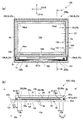
(液晶パネル100pおよび素子基板10の構成)
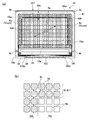
図2は、本発明の実施の形態1に係る液晶装置100の液晶パネル100pの説明図であり、図2(a)、(b)は各々、液晶パネル100pを各構成要素と共に対向基板の側から見た平面図、およびそのH−H′断面図である。図3は、本発明の実施の形態1に係る液晶装置100の素子基板10に形成されている電極等の説明図であり、図3(a)、(b)は、素子基板10全体に形成されている電極等の説明図、およびダミー画素電極の説明図である。なお、図3等においては画素電極9aの数等について少なく示してある。
(Configuration of liquid crystal panel 100p and element substrate 10)
FIG. 2 is an explanatory diagram of the liquid crystal panel 100p of the liquid crystal device 100 according to Embodiment 1 of the present invention. FIGS. 2A and 2B each show the liquid crystal panel 100p together with each component on the side of the counter substrate. It is the top view seen from and HH 'sectional drawing. FIG. 3 is an explanatory diagram of electrodes and the like formed on the element substrate 10 of the liquid crystal device 100 according to Embodiment 1 of the present invention. FIGS. 3 (a) and 3 (b) are formed on the entire element substrate 10. It is explanatory drawing of the electrode etc. which are used, and explanatory drawing of a dummy pixel electrode. Note that in FIG. 3 and the like, the number of pixel electrodes 9a is small.

図2に示すように、液晶パネル100pでは、素子基板10と対向基板20とが所定の隙間を介してシール材107によって貼り合わされており、シール材107は対向基板20の外縁に沿うように枠状に設けられている。シール材107は、光硬化樹脂や熱硬化性樹脂等からなる接着剤であり、両基板間の距離を所定値とするためのグラスファイバー、あるいはガラスビーズ等のギャップ材107aが配合されている。液晶パネル100pにおいて、素子基板10と対向基板20との間のうち、シール材107によって囲まれた領域内には液晶層50が保持されている。本形態において、シール材107には、液晶注入口として利用される途切れ部分107cが形成されており、かかる途切れ部分107cは、液晶材料の注入後、封止材108によって塞がれている。   As shown in FIG. 2, in the liquid crystal panel 100 p, the element substrate 10 and the counter substrate 20 are bonded to each other with a seal material 107 through a predetermined gap, and the seal material 107 is framed along the outer edge of the counter substrate 20. It is provided in the shape. The sealing material 107 is an adhesive made of a photo-curing resin, a thermosetting resin, or the like, and is mixed with a gap material 107a such as glass fiber or glass beads for setting the distance between both substrates to a predetermined value. In the liquid crystal panel 100p, the liquid crystal layer 50 is held in a region surrounded by the sealant 107 between the element substrate 10 and the counter substrate 20. In this embodiment, the sealing material 107 is formed with a discontinuous portion 107c used as a liquid crystal injection port, and the discontinuous portion 107c is closed by the sealing material 108 after the liquid crystal material is injected.

図2および図3(a)に示すように、液晶パネル100pにおいて、素子基板10および対向基板20はいずれも四角形であり、液晶パネル100pの略中央には、図1を参照して説明した画像表示領域10aが四角形の領域として設けられている。かかる形状に対応して、シール材107も略四角形に設けられ、画像表示領域10aの外側は、四角枠状の外周領域10cになっている。   As shown in FIGS. 2 and 3A, in the liquid crystal panel 100p, the element substrate 10 and the counter substrate 20 are both square, and the image described with reference to FIG. The display area 10a is provided as a rectangular area. Corresponding to this shape, the sealing material 107 is also provided in a substantially square shape, and the outer side of the image display area 10a is a rectangular frame-shaped outer peripheral area 10c.

素子基板10において、外周領域10cでは、素子基板10の一辺に沿ってデータ線駆動回路101および複数の端子102が形成されており、この一辺に隣接する他の辺に沿って走査線駆動回路104が形成されている。なお、端子102には、フレキシブル配線基板(図示せず)が接続されており、素子基板10には、フレキシブル配線基板を介して各種電位や各種信号が入力される。   In the element substrate 10, the data line driving circuit 101 and a plurality of terminals 102 are formed along one side of the element substrate 10 in the outer peripheral region 10 c, and the scanning line driving circuit 104 is formed along another side adjacent to the one side. Is formed. Note that a flexible wiring board (not shown) is connected to the terminal 102, and various potentials and various signals are input to the element substrate 10 through the flexible wiring board.

詳しくは後述するが、素子基板10の一方面10sおよび他方面10tのうち、対向基板20と対向する一方面10sの側において、画像表示領域10aには、図1を参照して説明した画素トランジスター30、および画素トランジスター30に電気的に接続する画素電極9aがマトリクス状に形成されており、かかる画素電極9aの上層側には配向膜16が形成されている。   As will be described in detail later, the pixel transistor described with reference to FIG. 1 is provided in the image display region 10a on the one surface 10s side of the element substrate 10 facing the counter substrate 20 out of the one surface 10s and the other surface 10t. 30 and pixel electrodes 9a electrically connected to the pixel transistors 30 are formed in a matrix, and an alignment film 16 is formed on the upper layer side of the pixel electrodes 9a.

また、素子基板10の一方面10sの側において、画像表示領域10aより外側の外周領域10cのうち、画像表示領域10aとシール材107とに挟まれた四角枠状の周辺領域10bには、画素電極9aと同時形成されたダミー画素電極9bが形成されている。   Further, on the one surface 10 s side of the element substrate 10, in the outer peripheral region 10 c outside the image display region 10 a, the rectangular frame-shaped peripheral region 10 b sandwiched between the image display region 10 a and the sealing material 107 includes pixels. A dummy pixel electrode 9b formed simultaneously with the electrode 9a is formed.

図3(b)に示すように、ダミー画素電極9bは、隣り合うダミー画素電極9b同士が細幅の連結部9uで繋がっている。かかるダミー画素電極9bは、素子基板10において配向膜16が形成される面を研磨により平坦化する際、画像表示領域10aと周辺領域10bとの高さ位置の差を圧縮し、配向膜16が形成される面を平坦面にするのに寄与する。本形態では、ダミー画素電極9bを利用して、後述するイオン性不純物トラップ用の第1電極81が構成されている。   As shown in FIG. 3B, in the dummy pixel electrode 9b, adjacent dummy pixel electrodes 9b are connected to each other by a narrow connecting portion 9u. The dummy pixel electrode 9b compresses the difference in height between the image display region 10a and the peripheral region 10b when the surface on which the alignment film 16 is formed on the element substrate 10 is flattened by polishing. This contributes to flattening the surface to be formed. In the present embodiment, a first electrode 81 for trapping ionic impurities, which will be described later, is configured using the dummy pixel electrode 9b.

再び図2において、対向基板20の一方面20sおよび他方面20tのうち、素子基板10と対向する一方面20sの側には共通電極21が形成されている。共通電極21は、対向基板20の略全面あるいは複数の帯状電極として複数の画素100aに跨って形成されている。本形態において、共通電極21は、対向基板20の略全面に形成されている。   In FIG. 2 again, the common electrode 21 is formed on the one surface 20 s facing the element substrate 10 out of the one surface 20 s and the other surface 20 t of the counter substrate 20. The common electrode 21 is formed across the plurality of pixels 100a as substantially the entire surface of the counter substrate 20 or a plurality of strip electrodes. In this embodiment, the common electrode 21 is formed on substantially the entire surface of the counter substrate 20.

また、対向基板20の一方面20sの側には、共通電極21の下層側に遮光層29が形成され、共通電極21の表面には配向膜26が積層されている。本形態において、遮光層29は、画像表示領域10aの外周縁に沿って延在する額縁部分29aとして形成されており、額縁部分29aの内周縁によって画像表示領域10aが規定されている。本形態において、遮光層29は、隣り合う画素電極9aにより挟まれた画素間領域10fに重なるブラックマトリクス部29bとしても形成されている。ここで、額縁部分29aはダミー画素電極9bと重なる位置に形成されており、額縁部分29aの外周縁は、シール材107の内周縁との間に隙間を隔てた位置にある。従って、額縁部分29aとシール材107とは重なっていない。   A light shielding layer 29 is formed on the lower side of the common electrode 21 on the one surface 20 s side of the counter substrate 20, and an alignment film 26 is laminated on the surface of the common electrode 21. In this embodiment, the light shielding layer 29 is formed as a frame portion 29a extending along the outer periphery of the image display region 10a, and the image display region 10a is defined by the inner periphery of the frame portion 29a. In this embodiment, the light shielding layer 29 is also formed as a black matrix portion 29b that overlaps the inter-pixel region 10f sandwiched between the adjacent pixel electrodes 9a. Here, the frame portion 29 a is formed at a position overlapping the dummy pixel electrode 9 b, and the outer peripheral edge of the frame portion 29 a is at a position with a gap between it and the inner peripheral edge of the sealing material 107. Therefore, the frame portion 29a and the sealing material 107 do not overlap.

液晶パネル100pにおいて、シール材107より外側には、対向基板20の一方面20sの側の4つの角部分に基板間導通用電極部25tが形成されており、素子基板10の一方面10sの側には、対向基板20の4つの角部分(基板間導通用電極部25t)と対向する位置に基板間導通用電極部6tが形成されている。本形態において、基板間導通用電極部25tは、共通電極21の一部からなる。基板間導通用電極部6tは、共通電位Vcomが印加された定電位配線6sに導通しており、定電位配線6sは、端子102のうち、共通電位印加用の端子102aに導通している。基板間導通用電極部6tと基板間導通用電極部25tとの間には、導電粒子を含んだ基板間導通材109が配置されており、対向基板20の共通電極21は、基板間導通用電極部6t、基板間導通材109および基板間導通用電極部25tを介して、素子基板10側に電気的に接続されている。このため、共通電極21は、素子基板10の側から共通電位Vcomが印加されている。シール材107は、略同一の幅寸法をもって対向基板20の外周縁に沿って設けられている。このため、シール材107は、略四角形である。但し、シール材107は、対向基板20の角部分と重なる領域では基板間導通用電極部6t、25tを避けて内側を通るように設けられており、シール材107の角部分は略円弧状である。   In the liquid crystal panel 100p, the inter-substrate conduction electrode portions 25t are formed on the four corners on the one surface 20s side of the counter substrate 20 outside the sealing material 107, and the element substrate 10 side on the one surface 10s side. The inter-substrate conduction electrode portion 6t is formed at a position facing the four corners of the counter substrate 20 (inter-substrate conduction electrode portion 25t). In this embodiment, the inter-substrate conduction electrode portion 25 t is formed of a part of the common electrode 21. The inter-substrate conduction electrode portion 6t is electrically connected to the constant potential wiring 6s to which the common potential Vcom is applied, and the constant potential wiring 6s is electrically connected to the common potential application terminal 102a among the terminals 102. An inter-substrate conducting material 109 containing conductive particles is disposed between the inter-substrate conducting electrode portion 6t and the inter-substrate conducting electrode portion 25t, and the common electrode 21 of the counter substrate 20 serves as an inter-substrate conducting electrode. It is electrically connected to the element substrate 10 side through the electrode portion 6t, the inter-substrate conducting material 109, and the inter-substrate conducting electrode portion 25t. Therefore, the common potential Vcom is applied to the common electrode 21 from the element substrate 10 side. The sealing material 107 is provided along the outer peripheral edge of the counter substrate 20 with substantially the same width dimension. For this reason, the sealing material 107 is substantially rectangular. However, the sealing material 107 is provided so as to pass through the inside avoiding the inter-substrate conduction electrode portions 6t and 25t in the region overlapping the corner portion of the counter substrate 20, and the corner portion of the sealing material 107 is substantially arc-shaped. is there.

かかる構成の液晶装置100において、本形態では、画素電極9aおよび共通電極21がITO(Indium Tin Oxide)膜やIZO(Indium Zinc Oxide)膜等の透光性導電膜により形成されており、液晶装置100は透過型の液晶装置である。かかる透過型の液晶装置100では、対向基板20の側から入射した光が素子基板10を透過して出射される間に変調されて画像を表示する。なお、画素電極9aおよび共通電極21のうち、例えば、共通電極21を透光性導電膜により形成し、画素電極9aをアルミニウム膜等の反射性導電膜により形成する場合もあり、かかる構成によれば、反射型の液晶装置100を構成することができる。反射型の液晶装置100では、素子基板10および対向基板20のうち、対向基板20の側から入射した光が素子基板10で反射して出射される間に変調されて画像を表示する。   In the liquid crystal device 100 having such a configuration, in this embodiment, the pixel electrode 9a and the common electrode 21 are formed of a light-transmitting conductive film such as an ITO (Indium Tin Oxide) film or an IZO (Indium Zinc Oxide) film. Reference numeral 100 denotes a transmissive liquid crystal device. In the transmissive liquid crystal device 100, light incident from the counter substrate 20 side is modulated while being transmitted through the element substrate 10 and emitted to display an image. Of the pixel electrode 9a and the common electrode 21, for example, the common electrode 21 may be formed of a light-transmitting conductive film, and the pixel electrode 9a may be formed of a reflective conductive film such as an aluminum film. In this case, the reflective liquid crystal device 100 can be configured. In the reflective liquid crystal device 100, light incident from the counter substrate 20 side of the element substrate 10 and the counter substrate 20 is modulated while being reflected by the element substrate 10 and emitted to display an image.

液晶装置100は、モバイルコンピューター、携帯電話機等といった電子機器のカラー表示装置として用いることができ、この場合、対向基板20あるいは素子基板10には、カラーフィルター(図示せず)が形成される。また、液晶装置100では、使用する液晶層50の種類や、ノーマリホワイトモード/ノーマリブラックモードの別に応じて、偏光フィルム、位相差フィルム、偏光板等が液晶パネル100pに対して所定の向きに配置される。さらに、液晶装置100は、後述する投射型表示装置(液晶プロジェクター)において、RGB用のライトバルブとして用いることができる。この場合、RGB用の各液晶装置100の各々には、RGB色分解用のダイクロイックミラーを介して分解された各色の光が投射光として各々入射されることになるので、カラーフィルターは形成されない。   The liquid crystal device 100 can be used as a color display device of an electronic device such as a mobile computer or a mobile phone. In this case, a color filter (not shown) is formed on the counter substrate 20 or the element substrate 10. Further, in the liquid crystal device 100, the polarizing film, the retardation film, the polarizing plate, etc. have a predetermined orientation with respect to the liquid crystal panel 100p according to the type of the liquid crystal layer 50 to be used and the normally white mode / normally black mode. Placed in. Furthermore, the liquid crystal device 100 can be used as a light valve for RGB in a projection display device (liquid crystal projector) described later. In this case, each color liquid crystal device 100 for RGB receives light of each color separated through RGB color separation dichroic mirrors as projection light, so that no color filter is formed.

本形態において、液晶装置100が、後述する投射型表示装置においてRGB用のライトバルブとして用いられる透過型の液晶装置であって、対向基板20から入射した光が素子基板10を透過して出射される場合を中心に説明する。また、本形態において、液晶装置100は、液晶層50の液晶分子として、誘電異方性が負のネマチック液晶化合物を用いたVAモードの液晶パネル100pを備えている場合を中心に説明する。   In this embodiment, the liquid crystal device 100 is a transmissive liquid crystal device used as a RGB light valve in a projection display device described later, and light incident from the counter substrate 20 is transmitted through the element substrate 10 and emitted. The case will be mainly described. Further, in the present embodiment, the liquid crystal device 100 will be described focusing on a case where the liquid crystal device 100 includes a VA mode liquid crystal panel 100p using a nematic liquid crystal compound having a negative dielectric anisotropy as the liquid crystal molecules of the liquid crystal layer 50.

(画素等の具体的構成)
図4は、本発明の実施の形態1に係る液晶装置100に用いた素子基板10において隣り合う複数の画素の平面図である。図5は、本発明の実施の形態1に係る液晶装置100の断面構成を示す説明図であり、図5(a)、(b)は、図4に示す画素のF−F′断面図、および外周領域10cの断面図である。なお、図4では、各層を以下の線
下層側の遮光層8a=細くて長い破線
半導体層1a=細くて短い点線
走査線3a=太い実線
ドレイン電極4a=細い実線
データ線6aおよび中継電極6b=細い一点鎖線
容量線5b=太い一点鎖線
上層側の遮光層7aおよび中継電極7b=細い二点鎖線
画素電極9a=太い破線
で示してある。また、図4では、互いの端部が重なり合う層については、層の形状等が分かりやすいように、端部の位置をずらしてある。
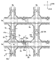
(Specific configuration of pixels, etc.)
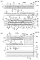
FIG. 4 is a plan view of a plurality of adjacent pixels in the element substrate 10 used in the liquid crystal device 100 according to Embodiment 1 of the present invention. 5 is an explanatory diagram showing a cross-sectional configuration of the liquid crystal device 100 according to Embodiment 1 of the present invention, and FIGS. 5A and 5B are cross-sectional views of the pixel shown in FIG. It is sectional drawing of the outer periphery area | region 10c. In FIG. 4, the light shielding layer 8a on the lower layer side = thin and long broken line Semiconductor layer 1a = thin and short dotted line Scan line 3a = thick solid line Drain electrode 4a = thin solid line Data line 6a and relay electrode 6b = Thin alternate long and short dashed lines Capacitance line 5b = thick alternate long and short dashed line Light-shielding layer 7a on the upper layer side and relay electrode 7b = thin alternate long and two short dashed line Pixel electrode 9a = shown by a thick broken line. In FIG. 4, the positions of the end portions of the layers overlapping with each other are shifted so that the shape of the layer can be easily understood.

図4に示すように、素子基板10において対向基板20と対向する一方面10sには、複数の画素100aの各々に画素電極9aが形成されており、隣り合う画素電極9aにより挟まれた画素間領域10fに沿ってデータ線6aおよび走査線3aが形成されている。本形態において、画素間領域10fは縦横に延在しており、走査線3aは画素間領域10fのうち、X方向(第1方向)に延在する第1画素間領域10gに沿って直線的に延在し、データ線6aは、Y方向(第2方向)に延在する第2画素間領域10hに沿って直線的に延在している。また、データ線6aと走査線3aとの交差に対応して画素トランジスター30が形成されており、本形態において、画素トランジスター30は、データ線6aと走査線3aとの交差領域およびその付近を利用して形成されている。素子基板10には容量線5bが形成されており、かかる容量線5bには共通電位Vcomが印加されている。本形態において、容量線5bは、走査線3aおよびデータ線6aに重なるように延在して格子状に形成されている。画素トランジスター30の上層側には遮光層7aが形成されており、かかる遮光層7aは、データ線6aに重なるように延在している。画素トランジスター30の下層側には遮光層8aが形成されており、かかる遮光層8aは、走査線3aと重なるように直線的に延びた主線部分と、データ線6aと走査線3aとの交差部分でデータ線6aに重なるように延びた副線部分とを備えている。   As shown in FIG. 4, on one surface 10 s of the element substrate 10 facing the counter substrate 20, pixel electrodes 9 a are formed on each of the plurality of pixels 100 a, and between the pixels sandwiched between adjacent pixel electrodes 9 a. A data line 6a and a scanning line 3a are formed along the region 10f. In this embodiment, the inter-pixel region 10f extends vertically and horizontally, and the scanning line 3a is linear along the first inter-pixel region 10g extending in the X direction (first direction) in the inter-pixel region 10f. The data line 6a extends linearly along the second inter-pixel region 10h extending in the Y direction (second direction). Further, a pixel transistor 30 is formed corresponding to the intersection of the data line 6a and the scanning line 3a. In this embodiment, the pixel transistor 30 uses the intersection region of the data line 6a and the scanning line 3a and its vicinity. Is formed. A capacitance line 5b is formed on the element substrate 10, and a common potential Vcom is applied to the capacitance line 5b. In this embodiment, the capacitor line 5b is formed in a lattice shape extending so as to overlap the scanning line 3a and the data line 6a. A light shielding layer 7a is formed on the upper layer side of the pixel transistor 30, and the light shielding layer 7a extends so as to overlap the data line 6a. A light shielding layer 8a is formed on the lower layer side of the pixel transistor 30, and the light shielding layer 8a is an intersection between the main line portion linearly extending so as to overlap the scanning line 3a and the data line 6a and the scanning line 3a. And a sub-line portion extending so as to overlap the data line 6a.

図5(a)に示すように、素子基板10は、石英基板やガラス基板等の透光性の基板本体10wの液晶層50側の基板面(対向基板20と対向する一方面10s側)に形成された画素電極9a、画素スイッチング用の画素トランジスター30、および配向膜16を主体として構成されている。対向基板20は、石英基板やガラス基板等の透光性の基板本体20w、その液晶層50側の表面(素子基板10と対向する一方面20s)に形成された遮光層29、共通電極21、および配向膜26を主体として構成されている。   As shown in FIG. 5A, the element substrate 10 is disposed on the substrate surface (on the one surface 10s facing the counter substrate 20) on the liquid crystal layer 50 side of the translucent substrate body 10w such as a quartz substrate or a glass substrate. The pixel electrode 9a, the pixel transistor 30 for pixel switching, and the alignment film 16 are mainly formed. The counter substrate 20 includes a translucent substrate body 20w such as a quartz substrate or a glass substrate, a light shielding layer 29 formed on a surface of the liquid crystal layer 50 side (one surface 20s facing the element substrate 10), a common electrode 21, And the alignment film 26 as a main component.

素子基板10において、基板本体10wの一方面10s側には、導電性のポリシリコン膜、金属シリサイド膜、金属膜あるいは金属化合物膜等の導電膜からなる下層側の遮光層8aが形成されている。本形態において、遮光層8aは、タングステンシリサイド(WSi)等の遮光膜からなり、液晶装置100を透過した後の光が他の部材で反射した際、かかる反射光が半導体層1aに入射して画素トランジスター30で光電流に起因する誤動作が発生することを防止する。なお、遮光層8aを走査線として構成する場合もあり、この場合、後述するゲート電極3cと遮光層8aを導通させた構成とする。   In the element substrate 10, a lower light shielding layer 8 a made of a conductive film such as a conductive polysilicon film, a metal silicide film, a metal film, or a metal compound film is formed on the one surface 10 s side of the substrate body 10 w. . In this embodiment, the light shielding layer 8a is made of a light shielding film such as tungsten silicide (WSi), and when the light after passing through the liquid crystal device 100 is reflected by another member, the reflected light is incident on the semiconductor layer 1a. The pixel transistor 30 is prevented from malfunctioning due to photocurrent. The light shielding layer 8a may be configured as a scanning line. In this case, the gate electrode 3c described later and the light shielding layer 8a are electrically connected.

基板本体10wの一方面10s側において、遮光層8aの上層側には、透光性の絶縁膜12が形成されており、かかる絶縁膜12の表面側に、半導体層1aを備えた画素トランジスター30が形成されている。本形態において、絶縁膜12は、NSG(ノンシリケートガラス)、PSG(リンシリケートガラス)、BSG(ボロンシリケートガラス)、BPSG (ボロンリンシリケートガラス)等のシリコン酸化膜(シリケートガラスも含む。)や、シリコン窒化膜からなる。かかる絶縁膜12は、シランガス(SiH4)、2塩化シラン(SiCl22)、TEOS(テトラエトキシシラン/テトラ・エチル・オルソ・シリケート/Si(OC254)、TEB(テトラ・エチル・ボートレート)、TMOP(テトラ・メチル・オキシ・フォスレート)等を用いた常圧CVD法、減圧CVD法、あるいはプラズマCVD法等により形成される。 A translucent insulating film 12 is formed on the upper surface side of the light shielding layer 8a on the one surface 10s side of the substrate body 10w, and the pixel transistor 30 including the semiconductor layer 1a on the surface side of the insulating film 12 is provided. Is formed. In this embodiment, the insulating film 12 is a silicon oxide film (including silicate glass) such as NSG (non-silicate glass), PSG (phosphorus silicate glass), BSG (boron silicate glass), or BPSG (boron phosphorus silicate glass). And made of a silicon nitride film. The insulating film 12 is formed of silane gas (SiH 4 ), silane dichloride (SiCl 2 H 2 ), TEOS (tetraethoxysilane / tetraethylorthosilicate / Si (OC 2 H 5 ) 4 ), TEB (tetra · It is formed by an atmospheric pressure CVD method, a low pressure CVD method, a plasma CVD method, or the like using ethyl boatrate), TMOP (tetramethyloxyphosphate), or the like.

画素トランジスター30は、データ線6aの延在方向に長辺方向を向けた半導体層1aと、半導体層1aの長さ方向と直交する方向に延在して半導体層1aの長さ方向の中央部分に重なるゲート電極3cとを備えており、本形態において、ゲート電極3cは走査線3aの一部からなる。画素トランジスター30は、半導体層1aとゲート電極3cとの間に透光性のゲート絶縁層2を有している。半導体層1aは、ゲート電極3cに対してゲート絶縁層2を介して対向するチャネル領域1gを備えているとともに、チャネル領域1gの両側にソース領域1bおよびドレイン領域1cを備えている。本形態において、画素トランジスター30は、LDD構造を有している。従って、ソース領域1bおよびドレイン領域1cは各々、チャネル領域1gの両側に低濃度領域を備え、低濃度領域に対してチャネル領域1gとは反対側で隣接する領域に高濃度領域を備えている。   The pixel transistor 30 includes a semiconductor layer 1a having a long side direction in the extending direction of the data line 6a, and a central portion in the length direction of the semiconductor layer 1a extending in a direction orthogonal to the length direction of the semiconductor layer 1a. In this embodiment, the gate electrode 3c is formed of a part of the scanning line 3a. The pixel transistor 30 has a translucent gate insulating layer 2 between the semiconductor layer 1a and the gate electrode 3c. The semiconductor layer 1a includes a channel region 1g opposed to the gate electrode 3c via the gate insulating layer 2, and includes a source region 1b and a drain region 1c on both sides of the channel region 1g. In this embodiment, the pixel transistor 30 has an LDD structure. Therefore, each of the source region 1b and the drain region 1c includes a low concentration region on both sides of the channel region 1g, and includes a high concentration region in a region adjacent to the low concentration region on the opposite side to the channel region 1g.

半導体層1aは、ポリシリコン膜(多結晶シリコン膜)等によって構成されている。ゲート絶縁層2は、半導体層1aを熱酸化したシリコン酸化膜からなる第1ゲート絶縁層2aと、温度が700〜900℃の高温条件での減圧CVD法により形成されたシリコン酸化膜からなる第2ゲート絶縁層2bとの2層構造からなる。ゲート電極3cおよび走査線3aは、導電性のポリシリコン膜、金属シリサイド膜、金属膜あるいは金属化合物膜等の導電膜からなる。本形態において、ゲート電極3cは、導電性のポリシリコン膜とタングステンシリサイド膜との2層構造を有している。   The semiconductor layer 1a is composed of a polysilicon film (polycrystalline silicon film) or the like. The gate insulating layer 2 includes a first gate insulating layer 2a made of a silicon oxide film obtained by thermally oxidizing the semiconductor layer 1a and a silicon oxide film made of a low pressure CVD method under a high temperature condition of 700 to 900 ° C. It has a two-layer structure with a two-gate insulating layer 2b. The gate electrode 3c and the scanning line 3a are made of a conductive film such as a conductive polysilicon film, a metal silicide film, a metal film, or a metal compound film. In this embodiment, the gate electrode 3c has a two-layer structure of a conductive polysilicon film and a tungsten silicide film.

ゲート電極3cの上層側には、NSG、PSG、BSG、BPSG等のシリコン酸化膜等からなる透光性の層間絶縁膜41が形成され、層間絶縁膜41の上層には、ドレイン電極4aが形成されている。本形態において、層間絶縁膜41は、シリコン酸化膜からなる。ドレイン電極4aは、導電性のポリシリコン膜、金属シリサイド膜、金属膜あるいは金属化合物膜等の導電膜からなる。本形態において、ドレイン電極4aはチタン窒化膜からなる。ドレイン電極4aは、半導体層1aのドレイン領域1c(画素電極側ソースドレイン領域)と一部が重なるように形成されており、層間絶縁膜41およびゲート絶縁層2を貫通するコンタクトホール41aを介してドレイン領域1cに導通している。   A translucent interlayer insulating film 41 made of a silicon oxide film such as NSG, PSG, BSG, or BPSG is formed on the upper layer side of the gate electrode 3c, and a drain electrode 4a is formed on the upper layer of the interlayer insulating film 41. Has been. In this embodiment, the interlayer insulating film 41 is made of a silicon oxide film. The drain electrode 4a is made of a conductive film such as a conductive polysilicon film, a metal silicide film, a metal film, or a metal compound film. In this embodiment, the drain electrode 4a is made of a titanium nitride film. The drain electrode 4 a is formed so as to partially overlap the drain region 1 c (pixel electrode side source / drain region) of the semiconductor layer 1 a, and through a contact hole 41 a penetrating the interlayer insulating film 41 and the gate insulating layer 2. It is electrically connected to the drain region 1c.

ドレイン電極4aの上層側には、シリコン酸化膜等からなる透光性のエッチングストッパー層49、および透光性の誘電体層40が形成されており、かかる誘電体層40の上層側には容量線5bが形成されている。誘電体層40としては、シリコン酸化膜やシリコン窒化膜等のシリコン化合物を用いることができる他、アルミニウム酸化膜、チタン酸化膜、タンタル酸化膜、ニオブ酸化膜、ハフニウム酸化膜、ランタン酸化膜、ジルコニウム酸化膜等の高誘電率の誘電体層を用いることができる。容量線5bは、導電性のポリシリコン膜、金属シリサイド膜、金属膜あるいは金属化合物膜等の導電膜からなる。本形態において、容量線5bは、チタン窒化膜、アルミニウム膜、およびチタン窒化膜との3層構造を有している。ここで、容量線5bは、誘電体層40を介してドレイン電極4aと重なっており、蓄積容量55を構成している。   A translucent etching stopper layer 49 made of a silicon oxide film or the like and a translucent dielectric layer 40 are formed on the upper layer side of the drain electrode 4a, and a capacitance is formed on the upper layer side of the dielectric layer 40. A line 5b is formed. As the dielectric layer 40, a silicon compound such as a silicon oxide film or a silicon nitride film can be used, and an aluminum oxide film, a titanium oxide film, a tantalum oxide film, a niobium oxide film, a hafnium oxide film, a lanthanum oxide film, zirconium A dielectric layer having a high dielectric constant such as an oxide film can be used. The capacitor line 5b is made of a conductive film such as a conductive polysilicon film, a metal silicide film, a metal film, or a metal compound film. In this embodiment, the capacitor line 5b has a three-layer structure of a titanium nitride film, an aluminum film, and a titanium nitride film. Here, the capacitor line 5 b overlaps with the drain electrode 4 a through the dielectric layer 40, and constitutes a storage capacitor 55.

容量線5bの上層側には層間絶縁膜42が形成されており、かかる層間絶縁膜42の上層側には、データ線6aと中継電極6bとが同一の導電膜により形成されている。層間絶縁膜42はシリコン酸化膜からなる。データ線6aと中継電極6bは、導電性のポリシリコン膜、金属シリサイド膜、金属膜あるいは金属化合物膜等の導電膜からなる。本形態において、データ線6aおよび中継電極6bは、アルミニウム合金膜や、チタン窒化膜とアルミニウム膜との2層乃至4層の積層膜からなる。データ線6aは、層間絶縁膜42、エッチングストッパー層49、層間絶縁膜41およびゲート絶縁層2を貫通するコンタクトホール42aを介してソース領域1b(データ線側ソースドレイン領域)に導通している。中継電極6bは、層間絶縁膜42およびエッチングストッパー層49を貫通するコンタクトホール42bを介してドレイン電極4aに導通している。   An interlayer insulating film 42 is formed on the upper layer side of the capacitor line 5b. On the upper layer side of the interlayer insulating film 42, the data line 6a and the relay electrode 6b are formed of the same conductive film. The interlayer insulating film 42 is made of a silicon oxide film. The data line 6a and the relay electrode 6b are made of a conductive film such as a conductive polysilicon film, a metal silicide film, a metal film, or a metal compound film. In this embodiment, the data line 6a and the relay electrode 6b are made of an aluminum alloy film or a laminated film of two to four layers of a titanium nitride film and an aluminum film. The data line 6a is electrically connected to the source region 1b (data line side source / drain region) through a contact hole 42a penetrating the interlayer insulating film 42, the etching stopper layer 49, the interlayer insulating film 41 and the gate insulating layer 2. The relay electrode 6 b is electrically connected to the drain electrode 4 a through a contact hole 42 b that penetrates the interlayer insulating film 42 and the etching stopper layer 49.

データ線6aおよび中継電極6bの上層側にはシリコン酸化膜等からなる透光性の層間絶縁膜44が形成されており、かかる層間絶縁膜44の上層側には、遮光層7aおよび中継電極7bが同一の導電膜によって形成されている。層間絶縁膜44は、例えば、テトラエトキシシランと酸素ガスとを用いたプラズマCVD法や、シランガスと亜酸化窒素ガスとを用いたプラズマCVD法等により形成したシリコン酸化膜からなり、その表面は平坦化されている。遮光層7aおよび中継電極7bは、導電性のポリシリコン膜、金属シリサイド膜、金属膜あるいは金属化合物膜等の導電膜からなる。本形態において、遮光層7aおよび中継電極7bは、アルミニウム合金膜や、チタン窒化膜とアルミニウム膜との2層乃至4層の積層膜からなる。中継電極7bは、層間絶縁膜44を貫通するコンタクトホール44aを介して中継電極6bに導通している。遮光層7aは、データ線6aと重なるように延在しており、遮光層として機能している。なお、遮光層7aを容量線5bと導通させてシールド層として利用してもよい。   A light-transmitting interlayer insulating film 44 made of a silicon oxide film or the like is formed on the upper side of the data line 6a and the relay electrode 6b. On the upper layer side of the interlayer insulating film 44, the light shielding layer 7a and the relay electrode 7b are formed. Are formed of the same conductive film. The interlayer insulating film 44 is made of, for example, a silicon oxide film formed by a plasma CVD method using tetraethoxysilane and oxygen gas or a plasma CVD method using silane gas and nitrous oxide gas, and the surface thereof is flat. It has become. The light shielding layer 7a and the relay electrode 7b are made of a conductive film such as a conductive polysilicon film, a metal silicide film, a metal film, or a metal compound film. In this embodiment, the light shielding layer 7a and the relay electrode 7b are made of an aluminum alloy film or a laminated film of two to four layers of a titanium nitride film and an aluminum film. The relay electrode 7 b is electrically connected to the relay electrode 6 b through a contact hole 44 a that penetrates the interlayer insulating film 44. The light shielding layer 7a extends so as to overlap the data line 6a, and functions as a light shielding layer. The light shielding layer 7a may be electrically connected to the capacitor line 5b and used as a shield layer.

遮光層7aおよび中継電極7bの上層側には、シリコン酸化膜等からなる透光性の層間絶縁膜45が形成されており、かかる層間絶縁膜45の上層側には、ITO膜等の透光性導電膜からなる画素電極9aが形成されている。本形態において、画素電極9aは、ITO膜からなる。層間絶縁膜45は、例えば、テトラエトキシシランと酸素ガスとを用いたプラズマCVD法や、シランガスと亜酸化窒素ガスとを用いたプラズマCVD法等により形成したシリコン酸化膜からなり、表面は平坦化されている。   A light-transmitting interlayer insulating film 45 made of a silicon oxide film or the like is formed on the upper side of the light shielding layer 7a and the relay electrode 7b, and a light-transmitting layer such as an ITO film is formed on the upper layer side of the interlayer insulating film 45. A pixel electrode 9a made of a conductive film is formed. In this embodiment, the pixel electrode 9a is made of an ITO film. The interlayer insulating film 45 is made of, for example, a silicon oxide film formed by a plasma CVD method using tetraethoxysilane and oxygen gas or a plasma CVD method using silane gas and nitrous oxide gas, and the surface is flattened. Has been.

画素電極9aは、中継電極7bと部分的に重なっており、層間絶縁膜45を貫通するコンタクトホール45aを介して中継電極7bに導通している。その結果、画素電極9aは、中継電極7b、中継電極6bおよびドレイン電極4aを介してドレイン領域1cに電気的に接続している。   The pixel electrode 9 a partially overlaps the relay electrode 7 b and is electrically connected to the relay electrode 7 b through a contact hole 45 a that penetrates the interlayer insulating film 45. As a result, the pixel electrode 9a is electrically connected to the drain region 1c through the relay electrode 7b, the relay electrode 6b, and the drain electrode 4a.

画素電極9aの表面には配向膜16が形成されている。本形態において、配向膜16は、SiOX(x<2)、SiO2、TiO2、MgO、Al23、In23、Sb23、Ta25等の斜方蒸着膜(傾斜垂直配向膜/無機配向膜)からなる。 An alignment film 16 is formed on the surface of the pixel electrode 9a. In this embodiment, the alignment film 16 is an obliquely deposited film of SiO x (x <2), SiO 2 , TiO 2 , MgO, Al 2 O 3 , In 2 O 3 , Sb 2 O 3 , Ta 2 O 5 or the like. (Inclined vertical alignment film / inorganic alignment film).

(対向基板20の構成)
対向基板20では、石英基板やガラス基板等の透光性の基板本体20w(透光性基板)の液晶層50側の表面(素子基板10に対向する一方面20s)には、遮光層29、シリコン酸化膜等からなる絶縁膜28、およびITO膜等の透光性導電膜からなる共通電極21が形成されており、かかる共通電極21を覆うように配向膜26が形成されている。本形態において、共通電極21はITO膜からなる。配向膜26は、配向膜16と同様、SiOX(x<2)、SiO2、TiO2、MgO、Al23、In23、Sb23、Ta25等の斜方蒸着膜(傾斜垂直配向膜/無機配向膜)である。かかる配向膜16、26は、配向規制力がアンチパラレルであり、液晶層50に用いた誘電異方性が負のネマチック液晶化合物を、図5に実線L1で液晶分子50bを模式的に示すように、傾斜垂直配向させる。このようにして、液晶パネル100pは、ノーマリブラックのVAモードの液晶パネルとして構成されている。本形態において、液晶分子50bのプレチルト方向は、図3に矢印Pで示すように、画像表示領域10aの4つの角10a1〜10a4のうち、対角に位置する2つの角10a1、10a3を結ぶ対角線方向に設定されている。
(Configuration of counter substrate 20)
In the counter substrate 20, a light shielding layer 29, a transparent substrate body 20 w (translucent substrate) such as a quartz substrate or a glass substrate, on the liquid crystal layer 50 side surface (one surface 20 s facing the element substrate 10), An insulating film 28 made of a silicon oxide film or the like and a common electrode 21 made of a light-transmitting conductive film such as an ITO film are formed. An alignment film 26 is formed so as to cover the common electrode 21. In this embodiment, the common electrode 21 is made of an ITO film. Similar to the alignment film 16, the alignment film 26 is oblique such as SiO x (x <2), SiO 2 , TiO 2 , MgO, Al 2 O 3 , In 2 O 3 , Sb 2 O 3 , and Ta 2 O 5. It is a deposited film (tilted vertical alignment film / inorganic alignment film). Such alignment films 16 and 26 schematically show a nematic liquid crystal compound having an alignment regulation force antiparallel and a negative dielectric anisotropy used for the liquid crystal layer 50, and a liquid crystal molecule 50b shown by a solid line L1 in FIG. And tilted vertically. In this way, the liquid crystal panel 100p is configured as a normally black VA mode liquid crystal panel. In the present embodiment, the pretilt direction of the liquid crystal molecules 50b is set such that two corners 10a 1 , 10a located diagonally out of the four corners 10a 1 to 10a 4 of the image display region 10a as indicated by an arrow P in FIG. It is set in the direction of the diagonal line connecting three .

(周辺領域10bの構成)
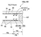
図3および図5(b)において、素子基板10の一方面10sの側において、画像表示領域10aとシール材107とに挟まれた周辺領域10bには、ダミー画素電極9bを利用して、画像表示領域10aの周りを囲むイオン性不純物トラップ用の第1電極81が形成されており、かかる第1電極81には、イオン性不純物トラップ用の電位Vipが印加されている。
(Configuration of the peripheral region 10b)
In FIG. 3 and FIG. 5B, the dummy pixel electrode 9b is used in the peripheral region 10b sandwiched between the image display region 10a and the sealing material 107 on the one surface 10s side of the element substrate 10 to display an image. A first electrode 81 for trapping ionic impurities is formed around the display region 10 a, and a potential Vip for trapping ionic impurities is applied to the first electrode 81.

図5(b)に示すように、対向基板20の一方面20sの側において、画像表示領域10aとシール材107とに挟まれた周辺領域10bにはイオン性不純物トラップ用の第2電極82が形成されており、かかる第2電極82は、第1電極81に対向している。本形態において、第2電極82は、共通電極21の一部を利用して構成されており、共通電位Vcomが印加されている。   As shown in FIG. 5B, the second electrode 82 for trapping ionic impurities is provided in the peripheral region 10b sandwiched between the image display region 10a and the sealing material 107 on the one surface 20s side of the counter substrate 20. The second electrode 82 is formed so as to face the first electrode 81. In this embodiment, the second electrode 82 is configured by using a part of the common electrode 21 and is applied with the common potential Vcom.

ここで、第1電極81と第2電極82とには異なる電位が印加されている。本形態において、共通電位Vcomは0Vであり、電位Vipは、−5V等の負の電位である。このため、共通電位Vcomおよび電位Vipは、以下の関係
電位Vip<共通電位Vcom
にある。
Here, different potentials are applied to the first electrode 81 and the second electrode 82. In this embodiment, the common potential Vcom is 0V, and the potential Vip is a negative potential such as −5V. Therefore, the common potential Vcom and the potential Vip are expressed by the following relational potential Vip <common potential Vcom.
It is in.

このように構成した液晶装置100において、素子基板10では、第1電極81の表面に配向膜16が形成されていない。すなわち、第1電極81は配向膜16の非形成領域に形成されており、液晶層50と直接、接している。また、第1電極81は、画素電極9aと同時形成されたITO膜(ダミー画素電極9b)からなる第1導電層811と、第1導電層811の上層側に積層された第1電荷注入層812とを備えており、第1電荷注入層812は液晶層50と接している。第1電荷注入層812は、ヒドロキシキノリン−アルミニウム錯体、アゾメチン−亜鉛錯体、あるいはジスチリルビフェニル誘導体からなる。かかる材料は、有機エレクトロルミネッセンス素子において電子注入層として用いられている材料であり、第1導電層811から液晶層50側に電子が移動する際のエネルギー障壁を低下させる機能を有している。本形態では、第1電荷注入層812としてヒドロキシキノリン−アルミニウム錯体層が形成されている。   In the liquid crystal device 100 configured as described above, in the element substrate 10, the alignment film 16 is not formed on the surface of the first electrode 81. That is, the first electrode 81 is formed in the non-formation region of the alignment film 16 and is in direct contact with the liquid crystal layer 50. The first electrode 81 includes a first conductive layer 811 made of an ITO film (dummy pixel electrode 9b) formed simultaneously with the pixel electrode 9a, and a first charge injection layer stacked on the upper layer side of the first conductive layer 811. 812, and the first charge injection layer 812 is in contact with the liquid crystal layer 50. The first charge injection layer 812 is made of a hydroxyquinoline-aluminum complex, an azomethine-zinc complex, or a distyrylbiphenyl derivative. Such a material is a material used as an electron injection layer in the organic electroluminescence element, and has a function of lowering an energy barrier when electrons move from the first conductive layer 811 to the liquid crystal layer 50 side. In this embodiment, a hydroxyquinoline-aluminum complex layer is formed as the first charge injection layer 812.

一方、対向基板20では、第2電極82の表面に配向膜26が形成されていない。すなわち、第2電極82は配向膜26の非形成領域に形成されており、液晶層50と直接、接している。また、第2電極82は、共通電極21を構成するITO膜の一部からなる第2導電層821と、第2導電層821の上層側に積層された第2電荷注入層822とを備えており、第2電荷注入層822は液晶層50と接している。第2電荷注入層822は、フタロシアニン化合物、トリアリルアミン化合物、ペリレン系化合物、あるいはユーロピウム錯体からなる。かかる材料は、有機エレクトロルミネッセンス素子において正孔注入層として用いられている材料であり、液晶層側から第2導電層821に電子が移動する際のエネルギー障壁を低下させる機能を有している。本形態では、第2電荷注入層822として銅フタロシアニン化合物層が形成されている。   On the other hand, in the counter substrate 20, the alignment film 26 is not formed on the surface of the second electrode 82. That is, the second electrode 82 is formed in a region where the alignment film 26 is not formed, and is in direct contact with the liquid crystal layer 50. The second electrode 82 includes a second conductive layer 821 made of a part of the ITO film constituting the common electrode 21, and a second charge injection layer 822 stacked on the upper side of the second conductive layer 821. The second charge injection layer 822 is in contact with the liquid crystal layer 50. The second charge injection layer 822 is made of a phthalocyanine compound, a triallylamine compound, a perylene compound, or a europium complex. Such a material is a material used as a hole injection layer in the organic electroluminescence element, and has a function of lowering an energy barrier when electrons move from the liquid crystal layer side to the second conductive layer 821. In this embodiment, a copper phthalocyanine compound layer is formed as the second charge injection layer 822.

なお、図示を省略するが、図1および図2を参照して説明したデータ線駆動回路101および走査線駆動回路104には、nチャネル型の駆動用トランジスターとpチャネル型の駆動用トランジスターとを備えた相補型トランジスター回路等が構成されている。ここで、駆動用トランジスターは、画素トランジスター30の製造工程の一部を利用して形成されたものである。このため、素子基板10においてデータ線駆動回路101および走査線駆動回路104が形成されている領域も、図5に示す断面構成と略同様な断面構成を有している。   Although not illustrated, the data line driver circuit 101 and the scan line driver circuit 104 described with reference to FIGS. 1 and 2 include an n-channel driving transistor and a p-channel driving transistor. Complementary transistor circuits and the like are provided. Here, the driving transistor is formed by utilizing a part of the manufacturing process of the pixel transistor 30. Therefore, the region where the data line driving circuit 101 and the scanning line driving circuit 104 are formed in the element substrate 10 also has a cross-sectional configuration substantially similar to the cross-sectional configuration shown in FIG.

(イオン性不純物のトラップおよび非イオン化)
図6は、本発明の実施の形態1に係る液晶装置100のイオン性不純物トラップ用の電極を模式的に示す説明図である。
(Ionic impurity trapping and non-ionization)
FIG. 6 is an explanatory view schematically showing electrodes for trapping ionic impurities of the liquid crystal device 100 according to Embodiment 1 of the present invention.

図5において、液晶層50に用いた液晶分子50bは、画素電極9aと共通電極21との間に印加される電圧が閾値電圧を超えると、実線L1で示す姿勢と点線L2で示す姿勢とに切り換わり、その結果、液晶層50には、矢印F1、F2で示す微弱な流動が発生する。このため、シール材107等から液晶層50内に溶出したイオン性不純物は、画像表示領域10aの角10a1、10a3に凝集しようとする。そこで、本形態の液晶装置100においては、画像を表示する際、あるいは液晶装置100を出荷する前の段階で、液晶装置100を動作させ、以下に説明するように、第1電極81と第2電極82との間に印加した電位によって、液晶層50において画像表示領域10aの内側に存在するイオン性不純物を画像表示領域10aの外側に引き寄せるとともに、引き寄せたイオン性不純物を非イオン性不純物に中性化する。 In FIG. 5, when the voltage applied between the pixel electrode 9a and the common electrode 21 exceeds the threshold voltage, the liquid crystal molecules 50b used in the liquid crystal layer 50 are changed to a posture indicated by a solid line L1 and a posture indicated by a dotted line L2. As a result, weak flow indicated by arrows F1 and F2 is generated in the liquid crystal layer 50. For this reason, the ionic impurities eluted into the liquid crystal layer 50 from the sealing material 107 or the like tend to aggregate at the corners 10a 1 and 10a 3 of the image display region 10a. Therefore, in the liquid crystal device 100 of the present embodiment, the liquid crystal device 100 is operated at the stage of displaying an image or before the liquid crystal device 100 is shipped, and the first electrode 81 and the second electrode as described below. The ionic impurities present inside the image display region 10a in the liquid crystal layer 50 are attracted to the outside of the image display region 10a by the potential applied between the electrode 82 and the ionic impurities attracted to the nonionic impurities. To become sexual.

より具体的には、図6に示すように、液晶装置100を動作させた際、素子基板10側の第1電極81にはイオン性不純物トラップ用の電位Vipが印加される一方、対向基板20の第2電極82には共通電位Vcomが印加され、共通電位Vcomおよび電位Vipは、以下の関係
電位Vip<共通電位Vcom
にある。従って、画像表示領域10a内のイオン性不純物のうち、正極性のイオン性不純物イオンMは、第1電極81に引き寄せられる一方、負極性のイオン性不純物イオンXは、第2電極82に引き寄せられる。ここで、第1電極81において、ITO膜からなる第1導電層811の上層側には第1電荷注入層812が形成されているため、第1電極81に引き寄せられた正極性のイオン性不純物イオンMは、下式
+e = M
に示すように、第1電極81から電子eを受け取り、非イオン性不純物Mとなる。また、第2電極82において、ITO膜からなる第2導電層821の上層側には第2電荷注入層822が形成されているため、第2電極82に引き寄せられた負極性のイオン性不純物イオンXは、下式
= X+e
に示すように、第2電極82に電子eを渡し、非イオン性不純物Xとなる。
More specifically, as shown in FIG. 6, when the liquid crystal device 100 is operated, the potential Vip for trapping ionic impurities is applied to the first electrode 81 on the element substrate 10 side, while the counter substrate 20. The common potential Vcom is applied to the second electrode 82, and the common potential Vcom and the potential Vip have the following relational potential Vip <common potential Vcom.
It is in. Accordingly, among the ionic impurities in the image display region 10 a, the positive ionic impurity ions M + are attracted to the first electrode 81, while the negative ionic impurity ions X are attracted to the second electrode 82. Gravitate. Here, in the first electrode 81, since the first charge injection layer 812 is formed on the upper side of the first conductive layer 811 made of an ITO film, the positive ionic impurity attracted to the first electrode 81 is formed. The ion M + is represented by the following formula: M + + e = M
As shown, the electron e is received from the first electrode 81 and becomes the nonionic impurity M. In addition, since the second charge injection layer 822 is formed on the second electrode 82 on the upper side of the second conductive layer 821 made of an ITO film, negative ionic impurity ions attracted to the second electrode 82 are formed. X represents the following formula: X = X + e
As shown, the electron e is transferred to the second electrode 82 and becomes a nonionic impurity X.

このように、画像表示領域10aの端部に凝集しようとするイオン性不純物M、Xは、画像表示領域10aの外側に引き寄せられるとともに、非イオン性不純物M、Xに中性化される。 As described above, the ionic impurities M + and X − that are to be aggregated at the end of the image display region 10 a are attracted to the outside of the image display region 10 a and are neutralized by the nonionic impurities M and X. .

(本形態の主な効果)
以上説明したように、本形態の液晶装置100において、素子基板10および対向基板20において画像表示領域10aとシール材107とに挟まれた周辺領域10bには、液晶層50に接する第1電極81および第2電極82が設けられ、かかる第1電極81および第2電極82には異なる電位が印加されている。このため、画像表示領域10aのイオン性不純物は、第1電極81および第2電極82に引き寄せられる。ここで、第1電極81は、第1導電層811に対して液晶層50が位置する側に第1電荷注入層812が積層された構造になっており、第2電極82は、第2導電層821に対して液晶層50が位置する側に第2電荷注入層822が積層された構造になっている。従って、第1電極81または第2電極82に引き寄せられたイオン性不純物は、第1電極81あるいは第2電極82との間で電荷の授受を行い、画像表示領域10aの外側で非イオン性不純物となる。それ故、イオン性不純物を静電的にトラップする構成と違って、画像表示領域10aの外側に排出されたイオン性不純物を消失させることができるので、画像表示領域10a内でイオン性不純物が凝集することを阻止する能力が高い。よって、本形態によれば、イオン性不純物の凝集を原因とする表示品位の低下が発生しにくい。
(Main effects of this form)
As described above, in the liquid crystal device 100 of the present embodiment, the first electrode 81 in contact with the liquid crystal layer 50 is disposed in the peripheral region 10b sandwiched between the image display region 10a and the sealing material 107 in the element substrate 10 and the counter substrate 20. And a second electrode 82, and different potentials are applied to the first electrode 81 and the second electrode 82. For this reason, the ionic impurities in the image display region 10 a are attracted to the first electrode 81 and the second electrode 82. Here, the first electrode 81 has a structure in which the first charge injection layer 812 is laminated on the side where the liquid crystal layer 50 is located with respect to the first conductive layer 811, and the second electrode 82 has the second conductive layer. The second charge injection layer 822 is stacked on the side where the liquid crystal layer 50 is located with respect to the layer 821. Accordingly, the ionic impurities attracted to the first electrode 81 or the second electrode 82 exchange charges with the first electrode 81 or the second electrode 82, and nonionic impurities are generated outside the image display region 10a. It becomes. Therefore, unlike the configuration in which the ionic impurities are electrostatically trapped, the ionic impurities discharged to the outside of the image display region 10a can be eliminated, and the ionic impurities are aggregated in the image display region 10a. High ability to prevent Therefore, according to this embodiment, it is difficult for display quality to be deteriorated due to aggregation of ionic impurities.

そこで、本形態の液晶装置100に対して、温度が80℃の条件でメタルハライドランプにより光照射(3W/cm2)を行う加速試験を行い、画像表示領域10aの周辺部に表示ムラが認識されるまでの時間を評価したところ、画像表示領域10aの周辺部に表示ムラが認識されるまでに2500時間という極めて長い時間を要した。これに対して、第1電極81および第2電極82に電位を印加しなかった参考例1について同様な加速試験を行ったところ、300時間で画像表示領域10aの周辺部に表示ムラが認識された。また、第1電極81および第2電極82に第1電荷注入層812および第2電荷注入層822を設けずに+5vの直流電圧を印加した参考例2について同様な加速試験を行ったところ、500時間で画像表示領域10aの周辺部に表示ムラが認識された。このように本形態によれば、イオン性不純物の凝集に起因する表示品位の低下が発生しにくいことを確認することができた。 Therefore, an acceleration test in which light irradiation (3 W / cm 2 ) is performed with a metal halide lamp at a temperature of 80 ° C. is performed on the liquid crystal device 100 of this embodiment, and display unevenness is recognized in the peripheral portion of the image display region 10a. As a result, it took a very long time of 2500 hours for display unevenness to be recognized in the periphery of the image display area 10a. On the other hand, when a similar acceleration test was performed on Reference Example 1 in which no potential was applied to the first electrode 81 and the second electrode 82, display unevenness was recognized in the peripheral portion of the image display region 10a in 300 hours. It was. A similar acceleration test was performed on Reference Example 2 in which a DC voltage of +5 v was applied to the first electrode 81 and the second electrode 82 without providing the first charge injection layer 812 and the second charge injection layer 822. Display unevenness was recognized in the periphery of the image display area 10a over time. As described above, according to the present embodiment, it was confirmed that display quality deterioration due to aggregation of ionic impurities hardly occurs.

[実施の形態2]
図7は、本発明の実施の形態2に係る液晶装置100のイオン性不純物トラップ用の電極を模式的に示す説明図である。本形態では、本発明における「第1基板」が対向基板20に相当し、「第2基板」が素子基板10に相当する。なお、本形態の基本的な構成は、実施の形態1と同様であるため、共通する部分には同一の符号を付して、それらの説明を省略する。
[Embodiment 2]
FIG. 7 is an explanatory view schematically showing electrodes for trapping ionic impurities of the liquid crystal device 100 according to Embodiment 2 of the present invention. In this embodiment, the “first substrate” in the present invention corresponds to the counter substrate 20, and the “second substrate” corresponds to the element substrate 10. Since the basic configuration of this embodiment is the same as that of Embodiment 1, common portions are denoted by the same reference numerals and description thereof is omitted.

図7に示すように、本形態の液晶装置100では、実施の形態1と逆に、対向基板20には、共通電極21を構成するITO膜の一部を利用して第1電極81が形成され、素子基板10にはダミー画素電極9bを利用して第2電極82が形成されている。このように構成した液晶装置100において、第1電極81と第2電極82とには異なる電位が印加されている。本形態において、第1電極81に印加された共通電位Vcomは0Vであり、第2電極82に印加された電位Vipは、+5V等の正の電位である。このため、共通電位Vcomおよび電位Vipは、以下の関係
電位Vip>共通電位Vcom
にある。
As shown in FIG. 7, in the liquid crystal device 100 of the present embodiment, the first electrode 81 is formed on the counter substrate 20 using a part of the ITO film constituting the common electrode 21, contrary to the first embodiment. The second electrode 82 is formed on the element substrate 10 using the dummy pixel electrode 9b. In the liquid crystal device 100 configured as described above, different potentials are applied to the first electrode 81 and the second electrode 82. In this embodiment, the common potential Vcom applied to the first electrode 81 is 0V, and the potential Vip applied to the second electrode 82 is a positive potential such as + 5V. Therefore, the common potential Vcom and the potential Vip are expressed by the following relational potential Vip> common potential Vcom
It is in.

ここで、対向基板20では、第1電極81の表面に配向膜26が形成されておらず、第1電極81は、液晶層50と直接、接している。また、第1電極81は、共通電極21と同時形成されたITO膜からなる第1導電層811と、第1導電層811の上層側に積層された第1電荷注入層812とを備えており、第1電荷注入層812は液晶層50と接している。第1電荷注入層812は、ヒドロキシキノリン−アルミニウム錯体、アゾメチン−亜鉛錯体、あるいはジスチリルビフェニル誘導体からなる。素子基板10では、第2電極82の表面に配向膜16が形成されておらず、第2電極82は、液晶層50と直接、接している。また、第2電極82は、ダミー画素電極9bを構成するITO膜からなる第2導電層821と、第2導電層821の上層側に積層された第2電荷注入層822とを備えており、第2電荷注入層822は液晶層50と接している。第2電荷注入層822は、フタロシアニン化合物、トリアリルアミン化合物、ペリレン系化合物、あるいはユーロピウム錯体からなる。   Here, in the counter substrate 20, the alignment film 26 is not formed on the surface of the first electrode 81, and the first electrode 81 is in direct contact with the liquid crystal layer 50. The first electrode 81 includes a first conductive layer 811 made of an ITO film simultaneously formed with the common electrode 21 and a first charge injection layer 812 stacked on the upper layer side of the first conductive layer 811. The first charge injection layer 812 is in contact with the liquid crystal layer 50. The first charge injection layer 812 is made of a hydroxyquinoline-aluminum complex, an azomethine-zinc complex, or a distyrylbiphenyl derivative. In the element substrate 10, the alignment film 16 is not formed on the surface of the second electrode 82, and the second electrode 82 is in direct contact with the liquid crystal layer 50. The second electrode 82 includes a second conductive layer 821 made of an ITO film constituting the dummy pixel electrode 9b, and a second charge injection layer 822 stacked on the upper side of the second conductive layer 821. The second charge injection layer 822 is in contact with the liquid crystal layer 50. The second charge injection layer 822 is made of a phthalocyanine compound, a triallylamine compound, a perylene compound, or a europium complex.

このように構成した液晶装置100を動作させた際、素子基板10側の第2電極82にはイオン性不純物トラップ用の電位Vipが印加される一方、対向基板20の第1電極81には共通電位Vcomが印加され、共通電位Vcomおよび電位Vipは、以下の関係
共通電位Vcom<電位Vip
にある。従って、画像表示領域10a内のイオン性不純物のうち、正極性のイオン性不純物イオンMは、第1電極81に引き寄せられ、第1電極81から電子eを受け取る結果、非イオン性不純物Mとなる。また、負極性のイオン性不純物イオンXは、第2電極82に引き寄せられ、第2電極82に電子eを渡す結果、非イオン性不純物Xとなる。従って、本形態の液晶装置100も、実施の形態1と同様な効果を奏する。
When the liquid crystal device 100 configured as described above is operated, the potential Vip for trapping ionic impurities is applied to the second electrode 82 on the element substrate 10 side, while the first electrode 81 of the counter substrate 20 is commonly used. The potential Vcom is applied, and the common potential Vcom and the potential Vip have the following relationship: common potential Vcom <potential Vip
It is in. Therefore, of the ionic impurities in the image display region 10a, M + is a positive ionic impurity ions are attracted to the first electrode 81, electrons e from the first electrode 81 - the receiving result, the non-ionic impurities M It becomes. Further, the negative ionic impurity ions X are attracted to the second electrode 82, and the electrons e are transferred to the second electrode 82, resulting in the nonionic impurities X. Therefore, the liquid crystal device 100 of the present embodiment also has the same effect as that of the first embodiment.

[実施の形態3]
図8は、本発明の実施の形態3に係る液晶装置100のイオン性不純物トラップ用の電極を模式的に示す説明図であり、図8(a)、(b)は、第1電極81が高電位である期間の説明図、および第1電極81が低電位である期間の説明図である。なお、本形態の基本的な構成は、実施の形態1と同様であるため、共通する部分には同一の符号を付して、それらの説明を省略する。
[Embodiment 3]
FIG. 8 is an explanatory view schematically showing an ionic impurity trapping electrode of the liquid crystal device 100 according to Embodiment 3 of the present invention. FIGS. 8A and 8B show the first electrode 81 as shown in FIG. It is explanatory drawing of the period when it is a high potential, and explanatory drawing of the period when the 1st electrode 81 is a low potential. Since the basic configuration of this embodiment is the same as that of Embodiment 1, common portions are denoted by the same reference numerals and description thereof is omitted.

図8(a)、(b)において、本形態の液晶装置100も、実施の形態1と同様、素子基板10には第1電極81が形成され、対向基板20には第2電極82が形成されている。また、第1電極81は、ITO膜からなる第1導電層811と、ヒドロキシキノリン−アルミニウム錯体、アゾメチン−亜鉛錯体、あるいはジスチリルビフェニル誘導体からなる第1電荷注入層812とを備えており、第1電荷注入層812は液晶層50と接している。第2電極82は、ITO膜からなる第2導電層821と、フタロシアニン化合物、トリアリルアミン化合物、ペリレン系化合物、あるいはユーロピウム錯体からなる第2電荷注入層822とを備えており、第2電荷注入層822は液晶層50と接している。   8A and 8B, in the liquid crystal device 100 of the present embodiment as well, the first electrode 81 is formed on the element substrate 10 and the second electrode 82 is formed on the counter substrate 20 as in the first embodiment. Has been. The first electrode 81 includes a first conductive layer 811 made of an ITO film, and a first charge injection layer 812 made of a hydroxyquinoline-aluminum complex, an azomethine-zinc complex, or a distyrylbiphenyl derivative. The one charge injection layer 812 is in contact with the liquid crystal layer 50. The second electrode 82 includes a second conductive layer 821 made of an ITO film, and a second charge injection layer 822 made of a phthalocyanine compound, a triallylamine compound, a perylene compound, or a europium complex. 822 is in contact with the liquid crystal layer 50.

このように構成した液晶装置100を動作させた際、対向基板20の第2電極82には定電位(0V)の共通電位Vcomが印加される一方、素子基板10側の第1電極81には、±5V等の交流の電位Vipが印加される。   When the liquid crystal device 100 configured as described above is operated, a common potential Vcom having a constant potential (0 V) is applied to the second electrode 82 of the counter substrate 20, while the first electrode 81 on the element substrate 10 side is applied to the first electrode 81. AC potential Vip such as ± 5V is applied.

従って、図8(a)に示すように、電位Vip>共通電位Vcomの期間では、正極性のイオン性不純物イオンMは、第2電極82に引き寄せられ、負極性のイオン性不純物イオンXは、第1電極81に引き寄せられる。 Therefore, as shown in FIG. 8A, during the period of the potential Vip> the common potential Vcom, the positive ionic impurity ions M + are attracted to the second electrode 82, and the negative ionic impurity ions X Is attracted to the first electrode 81.

これに対して、図8(b)に示すように、電位Vip<共通電位Vcomの期間では、正極性のイオン性不純物イオンMは、第1電極81に引き寄せられ、第1電極81から電子eを受け取る結果、非イオン性不純物Mとなる。また、負極性のイオン性不純物イオンXは、第2電極82に引き寄せられ、第2電極82に電子eを渡す結果、非イオン性不純物Xとなる。従って、本形態の液晶装置100も、実施の形態1と同様な効果を奏する。 On the other hand, as shown in FIG. 8B, in the period of potential Vip <common potential Vcom, positive ionic impurity ions M + are attracted to the first electrode 81 and electrons are transmitted from the first electrode 81. As a result of receiving e , it becomes a nonionic impurity M. Further, the negative ionic impurity ions X are attracted to the second electrode 82, and the electrons e are transferred to the second electrode 82, resulting in the nonionic impurities X. Therefore, the liquid crystal device 100 of the present embodiment also has the same effect as that of the first embodiment.

[実施の形態4]
図9は、本発明の実施の形態4に係る液晶装置100のイオン性不純物トラップ用の電極を模式的に示す説明図である。なお、本形態の基本的な構成は、実施の形態1と同様であるため、共通する部分には同一の符号を付して、それらの説明を省略する。
[Embodiment 4]
FIG. 9 is an explanatory diagram schematically showing electrodes for trapping ionic impurities of the liquid crystal device 100 according to Embodiment 4 of the present invention. Since the basic configuration of this embodiment is the same as that of Embodiment 1, common portions are denoted by the same reference numerals and description thereof is omitted.

上記実施の形態では、第1電極81および第2電極82が形成されている領域に配向膜16、26を設けないことにより、第1電極81および第2電極82が液晶層50に接する構造とした。これに対して、本形態では、図9に示すように、画像表示領域10aおよび周辺領域10bにシリコン酸化膜等の無機配向膜を斜方蒸着により形成することにより、斜めに延在する複数の凸部16aを備えたカラム構造の配向膜16が形成されている。かかる構成の配向膜16によれば、第1電荷注入層812が凸部16aの間16bで配向膜16から露出して液晶層50に接する構造となる。また、配向膜26についても、配向膜16と同様な構成とすれば、第2電荷注入層822が凸部26aの間26bで配向膜26から露出して液晶層50に接する構造となる。   In the above-described embodiment, the first electrode 81 and the second electrode 82 are in contact with the liquid crystal layer 50 by not providing the alignment films 16 and 26 in the region where the first electrode 81 and the second electrode 82 are formed. did. On the other hand, in the present embodiment, as shown in FIG. 9, a plurality of layers extending obliquely are formed by forming an inorganic alignment film such as a silicon oxide film in the image display region 10a and the peripheral region 10b by oblique deposition. An alignment film 16 having a column structure provided with convex portions 16a is formed. According to the alignment film 16 having such a configuration, the first charge injection layer 812 is exposed from the alignment film 16 at the interval 16b between the convex portions 16a and is in contact with the liquid crystal layer 50. Also, if the alignment film 26 has the same configuration as the alignment film 16, the second charge injection layer 822 is exposed from the alignment film 26 between the convex portions 26 a and is in contact with the liquid crystal layer 50.

[実施の形態5]
図10は、本発明の実施の形態5に係る液晶装置100のイオン性不純物トラップ用の電極を模式的に示す説明図である。なお、本形態の基本的な構成は、実施の形態1と同様であるため、共通する部分には同一の符号を付して、それらの説明を省略する。
[Embodiment 5]
FIG. 10 is an explanatory view schematically showing electrodes for trapping ionic impurities of the liquid crystal device 100 according to Embodiment 5 of the present invention. Since the basic configuration of this embodiment is the same as that of Embodiment 1, common portions are denoted by the same reference numerals and description thereof is omitted.

上記実施の形態では、第1電極81および第2電極82のうちの一方を素子基板10に設け、他方を対向基板20に設けたが、図10(a)に示すように、第1電極81および第2電極82の双方を素子基板10に設けた場合に本発明を適用してもよい。また、図10(b)に示すように、第1電極81および第2電極82の双方を対向基板20に設けた場合に本発明を適用してもよい。さらに、図10(a)、(b)に示す形態では、図示を省略するが、第1電極81および第2電極82が形成されている側の基板とは反対側の基板に、第1電極81および第2電極82と対向する対向電極を設け、かかる対向電極と第1電極81との間、および対向電極と第2電極82との間に電位を印加してもよい。   In the above embodiment, one of the first electrode 81 and the second electrode 82 is provided on the element substrate 10 and the other is provided on the counter substrate 20. However, as shown in FIG. The present invention may be applied when both the second electrode 82 and the second electrode 82 are provided on the element substrate 10. Further, as shown in FIG. 10B, the present invention may be applied when both the first electrode 81 and the second electrode 82 are provided on the counter substrate 20. Further, in the form shown in FIGS. 10A and 10B, although not shown, the first electrode is formed on the substrate opposite to the substrate on which the first electrode 81 and the second electrode 82 are formed. 81 and the second electrode 82 may be provided, and a potential may be applied between the counter electrode and the first electrode 81 and between the counter electrode and the second electrode 82.

[他の実施の形態]
上記実施の形態では、第1電極81および第2電極82を、画像表示領域10aを囲む全周に形成したが、プレチルト方向に位置する2つの角10a1、10a3のみに第1電極81および第2電極82を設けてもよい。また、上記実施の形態では、第1電極81および第2電極82を1つずつ設けたが、第1電極81および第2電極82の少なくとも一方を複数、設けてもよい。
[Other embodiments]
In the above embodiment, the first electrode 81 and the second electrode 82 are formed on the entire circumference surrounding the image display region 10a. However, the first electrode 81 and the second electrode 82 are provided only at the two corners 10a 1 and 10a 3 positioned in the pretilt direction. A second electrode 82 may be provided. Moreover, in the said embodiment, although the 1st electrode 81 and the 2nd electrode 82 were provided one each, you may provide at least one of the 1st electrode 81 and the 2nd electrode 82 more than one.

上記実施の形態では、透過型の液晶装置100に本発明を適用したが、反射型の液晶装置100に本発明を適用してもよい。   In the above embodiment, the present invention is applied to the transmissive liquid crystal device 100, but the present invention may be applied to the reflective liquid crystal device 100.

[電子機器への搭載例]
上述した実施形態に係る液晶装置100を適用した電子機器について説明する。図11は、本発明を適用した液晶装置100を用いた投射型表示装置の概略構成図であり、図11(a)、(b)は各々、透過型の液晶装置100を用いた投射型表示装置の説明図、および反射型の液晶装置100を用いた投射型表示装置の説明図である。
[Example of mounting on electronic devices]
An electronic apparatus to which the liquid crystal device 100 according to the above-described embodiment is applied will be described. FIG. 11 is a schematic configuration diagram of a projection display device using the liquid crystal device 100 to which the present invention is applied, and FIGS. 11A and 11B each show a projection display using the transmissive liquid crystal device 100. FIG. 2 is an explanatory diagram of the device and an explanatory diagram of a projection display device using the reflective liquid crystal device 100.

(投射型表示装置の第1例)
図11(a)に示す投射型表示装置110は、観察者側に設けられたスクリーン111に光を照射し、このスクリーン111で反射した光を観察する、いわゆる投影型の投射型表示装置である。投射型表示装置110は、光源112を備えた光源部130と、ダイクロイックミラー113、114と、液晶ライトバルブ115〜117(液晶装置100)と、投射光学系118と、クロスダイクロイックプリズム119と、リレー系120とを備えている。
(First example of projection display device)
A projection display device 110 shown in FIG. 11A is a so-called projection-type projection display device that irradiates light onto a screen 111 provided on the viewer side and observes light reflected by the screen 111. . The projection display device 110 includes a light source unit 130 including a light source 112, dichroic mirrors 113 and 114, liquid crystal light valves 115 to 117 (liquid crystal device 100), a projection optical system 118, a cross dichroic prism 119, and a relay. System 120.

光源112は、赤色光、緑色光及び青色光を含む光を供給する超高圧水銀ランプで構成されている。ダイクロイックミラー113は、光源112からの赤色光を透過させると共に緑色光及び青色光を反射する構成となっている。また、ダイクロイックミラー114は、ダイクロイックミラー113で反射された緑色光及び青色光のうち青色光を透過させると共に緑色光を反射する構成となっている。このように、ダイクロイックミラー113、114は、光源112から出射した光を赤色光と緑色光と青色光とに分離する色分離光学系を構成する。   The light source 112 is composed of an ultrahigh pressure mercury lamp that supplies light including red light, green light, and blue light. The dichroic mirror 113 is configured to transmit red light from the light source 112 and reflect green light and blue light. The dichroic mirror 114 is configured to transmit blue light and reflect green light among the green light and the blue light reflected by the dichroic mirror 113. Thus, the dichroic mirrors 113 and 114 constitute a color separation optical system that separates the light emitted from the light source 112 into red light, green light, and blue light.

ここで、ダイクロイックミラー113と光源112との間には、インテグレーター121及び偏光変換素子122が光源112から順に配置されている。インテグレーター121は、光源112から照射された光の照度分布を均一化する構成となっている。また、偏光変換素子122は、光源112からの光を例えばs偏光のような特定の振動方向を有する偏光にする構成となっている。   Here, between the dichroic mirror 113 and the light source 112, an integrator 121 and a polarization conversion element 122 are sequentially arranged from the light source 112. The integrator 121 is configured to uniformize the illuminance distribution of the light emitted from the light source 112. Further, the polarization conversion element 122 is configured to change the light from the light source 112 into polarized light having a specific vibration direction such as s-polarized light.

液晶ライトバルブ115は、ダイクロイックミラー113を透過して反射ミラー123で反射した赤色光を画像信号に応じて変調する透過型の液晶装置100である。液晶ライトバルブ115は、λ/2位相差板115a、第1偏光板115b、液晶パネル115c及び第2偏光板115dを備えている。ここで、液晶ライトバルブ115に入射する赤色光は、ダイクロイックミラー113を透過しても光の偏光は変化しないことから、s偏光のままである。   The liquid crystal light valve 115 is a transmissive liquid crystal device 100 that modulates red light transmitted through the dichroic mirror 113 and reflected by the reflection mirror 123 in accordance with an image signal. The liquid crystal light valve 115 includes a λ / 2 phase difference plate 115a, a first polarizing plate 115b, a liquid crystal panel 115c, and a second polarizing plate 115d. Here, the red light incident on the liquid crystal light valve 115 remains s-polarized light because the polarization of the light does not change even if it passes through the dichroic mirror 113.

λ/2位相差板115aは、液晶ライトバルブ115に入射したs偏光をp偏光に変換する光学素子である。また、第1偏光板115bは、s偏光を遮断してp偏光を透過させる偏光板である。そして、液晶パネル115cは、p偏光を画像信号に応じた変調によってs偏光(中間調であれば円偏光又は楕円偏光)に変換する構成となっている。さらに、第2偏光板115dは、p偏光を遮断してs偏光を透過させる偏光板である。したがって、液晶ライトバルブ115は、画像信号に応じて赤色光を変調し、変調した赤色光をクロスダイクロイックプリズム119に向けて出射する構成となっている。   The λ / 2 phase difference plate 115a is an optical element that converts s-polarized light incident on the liquid crystal light valve 115 into p-polarized light. The first polarizing plate 115b is a polarizing plate that blocks s-polarized light and transmits p-polarized light. The liquid crystal panel 115c is configured to convert p-polarized light into s-polarized light (circularly polarized light or elliptically polarized light in the case of halftone) by modulation according to the image signal. Furthermore, the second polarizing plate 115d is a polarizing plate that blocks p-polarized light and transmits s-polarized light. Therefore, the liquid crystal light valve 115 is configured to modulate the red light according to the image signal and emit the modulated red light toward the cross dichroic prism 119.

なお、λ/2位相差板115a及び第1偏光板115bは、偏光を変換させない透光性のガラス板115eに接した状態で配置されており、λ/2位相差板115a及び第1偏光板115bが発熱によって歪むのを回避することができる。   Note that the λ / 2 phase difference plate 115a and the first polarizing plate 115b are disposed in contact with a light-transmitting glass plate 115e that does not convert polarized light, and the λ / 2 phase difference plate 115a and the first polarizing plate 115b. It is possible to avoid distortion of 115b due to heat generation.

液晶ライトバルブ116は、ダイクロイックミラー113で反射した後にダイクロイックミラー114で反射した緑色光を画像信号に応じて変調する透過型の液晶装置100である。そして、液晶ライトバルブ116は、液晶ライトバルブ115と同様に、第1偏光板116b、液晶パネル116c及び第2偏光板116dを備えている。液晶ライトバルブ116に入射する緑色光は、ダイクロイックミラー113、114で反射されて入射するs偏光である。第1偏光板116bは、p偏光を遮断してs偏光を透過させる偏光板である。また、液晶パネル116cは、s偏光を画像信号に応じた変調によってp偏光(中間調であれば円偏光又は楕円偏光)に変換する構成となっている。そして、第2偏光板116dは、s偏光を遮断してp偏光を透過させる偏光板である。したがって、液晶ライトバルブ116は、画像信号に応じて緑色光を変調し、変調した緑色光をクロスダイクロイックプリズム119に向けて出射する構成となっている。   The liquid crystal light valve 116 is a transmissive liquid crystal device 100 that modulates green light reflected by the dichroic mirror 114 after being reflected by the dichroic mirror 113 in accordance with an image signal. Similarly to the liquid crystal light valve 115, the liquid crystal light valve 116 includes a first polarizing plate 116b, a liquid crystal panel 116c, and a second polarizing plate 116d. Green light incident on the liquid crystal light valve 116 is s-polarized light that is reflected by the dichroic mirrors 113 and 114 and then incident. The first polarizing plate 116b is a polarizing plate that blocks p-polarized light and transmits s-polarized light. The liquid crystal panel 116c is configured to convert s-polarized light into p-polarized light (circularly polarized light or elliptically polarized light in the case of halftone) by modulation according to the image signal. The second polarizing plate 116d is a polarizing plate that blocks s-polarized light and transmits p-polarized light. Accordingly, the liquid crystal light valve 116 is configured to modulate green light in accordance with the image signal and emit the modulated green light toward the cross dichroic prism 119.

液晶ライトバルブ117は、ダイクロイックミラー113で反射し、ダイクロイックミラー114を透過した後でリレー系120を経た青色光を画像信号に応じて変調する透過型の液晶装置100である。そして、液晶ライトバルブ117は、液晶ライトバルブ115、116と同様に、λ/2位相差板117a、第1偏光板117b、液晶パネル117c及び第2偏光板117dを備えている。ここで、液晶ライトバルブ117に入射する青色光は、ダイクロイックミラー113で反射してダイクロイックミラー114を透過した後にリレー系120の後述する2つの反射ミラー125a、125bで反射することから、s偏光となっている。   The liquid crystal light valve 117 is a transmissive liquid crystal device 100 that modulates blue light reflected by the dichroic mirror 113 and transmitted through the dichroic mirror 114 and then through the relay system 120 in accordance with an image signal. Similarly to the liquid crystal light valves 115 and 116, the liquid crystal light valve 117 includes a λ / 2 retardation film 117a, a first polarizing plate 117b, a liquid crystal panel 117c, and a second polarizing plate 117d. Here, since the blue light incident on the liquid crystal light valve 117 is reflected by the two reflecting mirrors 125a and 125b described later of the relay system 120 after being reflected by the dichroic mirror 113 and transmitted through the dichroic mirror 114, the s-polarized light is reflected. It has become.

λ/2位相差板117aは、液晶ライトバルブ117に入射したs偏光をp偏光に変換する光学素子である。また、第1偏光板117bは、s偏光を遮断してp偏光を透過させる偏光板である。そして、液晶パネル117cは、p偏光を画像信号に応じた変調によってs偏光(中間調であれば円偏光又は楕円偏光)に変換する構成となっている。さらに、第2偏光板117dは、p偏光を遮断してs偏光を透過させる偏光板である。したがって、液晶ライトバルブ117は、画像信号に応じて青色光を変調し、変調した青色光をクロスダイクロイックプリズム119に向けて出射する構成となっている。なお、λ/2位相差板117a及び第1偏光板117bは、ガラス板117eに接した状態で配置されている。   The λ / 2 phase difference plate 117a is an optical element that converts s-polarized light incident on the liquid crystal light valve 117 into p-polarized light. The first polarizing plate 117b is a polarizing plate that blocks s-polarized light and transmits p-polarized light. The liquid crystal panel 117c is configured to convert p-polarized light into s-polarized light (circularly polarized light or elliptically polarized light in the case of halftone) by modulation according to the image signal. Furthermore, the second polarizing plate 117d is a polarizing plate that blocks p-polarized light and transmits s-polarized light. Accordingly, the liquid crystal light valve 117 is configured to modulate blue light in accordance with an image signal and emit the modulated blue light toward the cross dichroic prism 119. The λ / 2 phase difference plate 117a and the first polarizing plate 117b are disposed in contact with the glass plate 117e.

リレー系120は、リレーレンズ124a、124bと反射ミラー125a、125bとを備えている。リレーレンズ124a、124bは、青色光の光路が長いことによる光損失を防止するために設けられている。ここで、リレーレンズ124aは、ダイクロイックミラー114と反射ミラー125aとの間に配置されている。また、リレーレンズ124bは、反射ミラー125a、125bの間に配置されている。反射ミラー125aは、ダイクロイックミラー114を透過してリレーレンズ124aから出射した青色光をリレーレンズ124bに向けて反射するように配置されている。また、反射ミラー125bは、リレーレンズ124bから出射した青色光を液晶ライトバルブ117に向けて反射するように配置されている。   The relay system 120 includes relay lenses 124a and 124b and reflection mirrors 125a and 125b. The relay lenses 124a and 124b are provided to prevent light loss due to a long blue light path. Here, the relay lens 124a is disposed between the dichroic mirror 114 and the reflection mirror 125a. The relay lens 124b is disposed between the reflection mirrors 125a and 125b. The reflection mirror 125a is disposed so as to reflect the blue light transmitted through the dichroic mirror 114 and emitted from the relay lens 124a toward the relay lens 124b. The reflection mirror 125b is arranged to reflect the blue light emitted from the relay lens 124b toward the liquid crystal light valve 117.

クロスダイクロイックプリズム119は、2つのダイクロイック膜119a、119bをX字型に直交配置した色合成光学系である。ダイクロイック膜119aは青色光を反射して緑色光を透過する膜であり、ダイクロイック膜119bは赤色光を反射して緑色光を透過する膜である。したがって、クロスダイクロイックプリズム119は、液晶ライトバルブ115〜117のそれぞれで変調された赤色光と緑色光と青色光とを合成し、投射光学系118に向けて出射するように構成されている。   The cross dichroic prism 119 is a color combining optical system in which two dichroic films 119a and 119b are arranged orthogonally in an X shape. The dichroic film 119a is a film that reflects blue light and transmits green light, and the dichroic film 119b is a film that reflects red light and transmits green light. Therefore, the cross dichroic prism 119 is configured to combine the red light, the green light, and the blue light modulated by the liquid crystal light valves 115 to 117 and emit the resultant light toward the projection optical system 118.

なお、液晶ライトバルブ115、117からクロスダイクロイックプリズム119に入射する光はs偏光であり、液晶ライトバルブ116からクロスダイクロイックプリズム119に入射する光はp偏光である。このようにクロスダイクロイックプリズム119に入射する光を異なる種類の偏光としていることで、クロスダイクロイックプリズム119において各液晶ライトバルブ115〜117から入射する光を合成できる。ここで、一般に、ダイクロイック膜119a、119bはs偏光の反射トランジスター特性に優れている。このため、ダイクロイック膜119a、119bで反射される赤色光及び青色光をs偏光とし、ダイクロイック膜119a、119bを透過する緑色光をp偏光としている。投射光学系118は、投影レンズ(図示略)を有しており、クロスダイクロイックプリズム119で合成された光をスクリーン111に投射するように構成されている。   Note that light incident on the cross dichroic prism 119 from the liquid crystal light valves 115 and 117 is s-polarized light, and light incident on the cross dichroic prism 119 from the liquid crystal light valve 116 is p-polarized light. Thus, by making the light incident on the cross dichroic prism 119 into different types of polarized light, the light incident from the liquid crystal light valves 115 to 117 in the cross dichroic prism 119 can be synthesized. Here, in general, the dichroic films 119a and 119b are excellent in s-polarized reflection transistor characteristics. Therefore, red light and blue light reflected by the dichroic films 119a and 119b are s-polarized light, and green light transmitted through the dichroic films 119a and 119b is p-polarized light. The projection optical system 118 has a projection lens (not shown) and is configured to project the light combined by the cross dichroic prism 119 onto the screen 111.

(投射型表示装置の第2例)
図11(b)に示す投射型表示装置1000は、光源光を発生する光源部1021と、光源部1021から出射された光源光を赤、緑、青の3色に分離する色分離導光光学系1023と、色分離導光光学系1023から出射された各色の光源光によって照明される光変調部1025とを有している。また、投射型表示装置1000は、光変調部1025から出射された各色の像光を合成するクロスダイクロイックプリズム1027(合成光学系)と、クロスダイクロイックプリズム1027を経た像光をスクリーン(不図示)に投射するための投射光学系である投射光学系1029とを備えている。
(Second example of projection display device)
A projection display device 1000 shown in FIG. 11B includes a light source unit 1021 that generates light source light and a color separation light guide optical that separates the light source light emitted from the light source unit 1021 into three colors of red, green, and blue. A system 1023 and a light modulation unit 1025 illuminated by the light source light of each color emitted from the color separation light guide optical system 1023 are provided. In addition, the projection display apparatus 1000 uses a cross dichroic prism 1027 (combining optical system) that combines the image light of each color emitted from the light modulation unit 1025 and the image light that has passed through the cross dichroic prism 1027 on a screen (not shown). A projection optical system 1029 which is a projection optical system for projecting.

かかる投射型表示装置1000において、光源部1021は、光源1021aと、一対のフライアイ光学系1021d、1021eと、偏光変換部材1021gと、重畳レンズ1021iとを備えている。本形態においては、光源部1021は、放物面からなるリフレクタ1021fを備えており、平行光を出射する。フライアイ光学系1021d、1021eは、システム光軸と直交する面内にマトリクス状に配置された複数の要素レンズからなり、これらの要素レンズによって光源光を分割して個別に集光・発散させる。偏光変換部材1021gは、フライアイ光学系1021eから出射した光源光を、例えば図面に平行なp偏光成分のみに変換して光路下流側光学系に供給する。重畳レンズ1021iは、偏光変換部材1021gを経た光源光を全体として適宜収束させることにより、光変調部1025に設けた複数の液晶装置100を各々均一に重畳照明可能とする。   In the projection display apparatus 1000, the light source unit 1021 includes a light source 1021a, a pair of fly-eye optical systems 1021d and 1021e, a polarization conversion member 1021g, and a superimposing lens 1021i. In the present embodiment, the light source unit 1021 includes a reflector 1021f having a paraboloid and emits parallel light. The fly-eye optical systems 1021d and 1021e are composed of a plurality of element lenses arranged in a matrix in a plane orthogonal to the system optical axis, and the light source light is divided and condensed and diverged individually by these element lenses. The polarization conversion member 1021g converts the light source light emitted from the fly-eye optical system 1021e into, for example, only a p-polarized component parallel to the drawing, and supplies it to the optical path downstream optical system. The superimposing lens 1021i allows the plurality of liquid crystal devices 100 provided in the light modulation unit 1025 to uniformly illuminate each other by appropriately converging the light source light that has passed through the polarization conversion member 1021g as a whole.

色分離導光光学系1023は、クロスダイクロイックミラー1023aと、ダイクロイックミラー1023bと、反射ミラー1023j、1023kとを備える。色分離導光光学系1023において、光源部1021からの略白色の光源光は、クロスダイクロイックミラー1023aに入射する。クロスダイクロイックミラー1023aを構成する一方の第1ダイクロイックミラー1031aで反射された赤色(R)の光は、反射ミラー1023jで反射されダイクロイックミラー1023bを透過して、入射側偏光板1037r、p偏光を透過させ、s偏光を反射するワイヤーグリッド偏光板1032r、および光学補償板1039rを介して、p偏光のまま、赤色(R)用の液晶装置100に入射する。   The color separation light guide optical system 1023 includes a cross dichroic mirror 1023a, a dichroic mirror 1023b, and reflection mirrors 1023j and 1023k. In the color separation light guide optical system 1023, the substantially white light source light from the light source unit 1021 enters the cross dichroic mirror 1023a. The red (R) light reflected by one of the first dichroic mirrors 1031a constituting the cross dichroic mirror 1023a is reflected by the reflecting mirror 1023j, passes through the dichroic mirror 1023b, and passes through the incident side polarizing plate 1037r and the p-polarized light. Then, the light is incident on the red (R) liquid crystal device 100 as p-polarized light through the wire grid polarizer 1032r that reflects s-polarized light and the optical compensation plate 1039r.

また、第1ダイクロイックミラー1031aで反射された緑色(G)の光は、反射ミラー1023jで反射され、その後、ダイクロイックミラー1023bでも反射されて、入射側偏光板1037g、p偏光を透過させ、s偏光を反射するワイヤーグリッド偏光板1032g、および光学補償板1039gを介して、p偏光のまま、緑色(G)用の液晶装置100に入射する。   Further, the green (G) light reflected by the first dichroic mirror 1031a is reflected by the reflection mirror 1023j, and then also reflected by the dichroic mirror 1023b to transmit the incident side polarizing plate 1037g and p-polarized light, and s-polarized light. Is incident on the green (G) liquid crystal device 100 as p-polarized light through the wire grid polarizing plate 1032g and the optical compensation plate 1039g.

これに対して、クロスダイクロイックミラー1023aを構成する他方の第2ダイクロイックミラー1031bで反射された青色(B)の光は、反射ミラー1023kで反射されて、入射側偏光板1037b、p偏光を透過する一方でs偏光を反射するワイヤーグリッド偏光板1032b、および光学補償板1039bを介して、p偏光のまま、青色(B)用の液晶装置100に入射する。なお、光学補償板1039r、1039g、1039bは、液晶装置100への入射光および出射光の偏光状態を調整することで、液晶層の特性を光学的に補償している。   On the other hand, the blue (B) light reflected by the other second dichroic mirror 1031b constituting the cross dichroic mirror 1023a is reflected by the reflection mirror 1023k and passes through the incident side polarizing plate 1037b and the p-polarized light. On the other hand, it enters the liquid crystal device 100 for blue (B) as p-polarized light through the wire grid polarizing plate 1032b that reflects s-polarized light and the optical compensation plate 1039b. Note that the optical compensation plates 1039r, 1039g, and 1039b optically compensate the characteristics of the liquid crystal layer by adjusting the polarization states of the incident light and the emitted light to the liquid crystal device 100.

このように構成した投射型表示装置1000では、光学補償板1039r、1039g、1039bを経て入射した3色の光は各々、各液晶装置100において変調される。その際、液晶装置100から出射された変調光のうち、s偏光の成分光は、ワイヤーグリッド偏光板1032r、1032g、1032bで反射し、出射側偏光板1038r、1038g、1038bを介してクロスダイクロイックプリズム1027に入射する。クロスダイクロイックプリズム1027には、X字状に交差する第1誘電体多層膜1027aおよび第2誘電体多層膜1027bが形成されており、一方の第1誘電体多層膜1027aはR光を反射し、他方の第2誘電体多層膜1027bはB光を反射する。従って、3色の光は、クロスダイクロイックプリズム1027において合成され、投射光学系1029に出射される。そして、投射光学系1029は、クロスダイクロイックプリズム1027で合成されたカラーの像光を、所望の倍率でスクリーン(図示せず。)投射する。   In the projection display apparatus 1000 configured as described above, the three colors of light incident through the optical compensation plates 1039r, 1039g, and 1039b are modulated in the liquid crystal devices 100, respectively. At that time, of the modulated light emitted from the liquid crystal device 100, the s-polarized component light is reflected by the wire grid polarizing plates 1032r, 1032g, and 1032b, and crossed dichroic prisms via the outgoing-side polarizing plates 1038r, 1038g, and 1038b. Incident at 1027. In the cross dichroic prism 1027, a first dielectric multilayer film 1027a and a second dielectric multilayer film 1027b intersecting in an X shape are formed, and the first dielectric multilayer film 1027a reflects R light, The other second dielectric multilayer film 1027b reflects B light. Therefore, the three colors of light are combined by the cross dichroic prism 1027 and emitted to the projection optical system 1029. The projection optical system 1029 projects the color image light synthesized by the cross dichroic prism 1027 on a screen (not shown) at a desired magnification.

(他の投射型表示装置)
なお、投射型表示装置については、光源部として、各色の光を出射するLED光源等を用い、かかるLED光源から出射された色光を各々、別の液晶装置に供給するように構成してもよい。
(Other projection display devices)
In addition, about a projection type display apparatus, you may comprise the LED light source etc. which radiate | emit the light of each color as a light source part, and supply each color light radiate | emitted from this LED light source to another liquid crystal device. .

(他の電子機器)
本発明を適用した液晶装置100については、上記の電子機器の他にも、携帯電話機、情報携帯端末(PDA:Personal Digital Assistants)、デジタルカメラ、液晶テレビ、カーナビゲーション装置、テレビ電話、POS端末、タッチパネルを備えた機器等の電子機器において直視型表示装置として用いてもよい。
(Other electronic devices)
As for the liquid crystal device 100 to which the present invention is applied, in addition to the electronic devices described above, mobile phones, personal digital assistants (PDAs), digital cameras, liquid crystal televisions, car navigation devices, video phones, POS terminals, You may use as a direct view type | mold display apparatus in electronic devices, such as an apparatus provided with the touch panel.

9a・・画素電極、9b・・ダミー画素電極、10・・素子基板、10a・・画像表示領域、10b・・周辺領域、20・・対向基板、21・・共通電極、50・・液晶層、81・・第1電極、82・・第2電極、107・・シール材、100・・液晶装置、110、1000・・投射型表示装置 9a ... Pixel electrode, 9b ... Dummy pixel electrode, 10 ... Element substrate, 10a ... Image display area, 10b ... Peripheral area, 20 ... Counter substrate, 21 ... Common electrode, 50 ... Liquid crystal layer, 81..First electrode 82..Second electrode 107..Sealant 100..Liquid crystal device 110, 1000..Projection type display device

Claims (10)

画像表示領域に画素電極および配向膜が設けられた素子基板と、
前記画像表示領域に共通電極および配向膜が設けられた対向基板と、
前記素子基板と前記対向基板とを貼り合わせるシール材と、
前記素子基板と前記対向基板との間において前記シール材で囲まれた領域内に保持された液晶層と、
前記素子基板および前記対向基板のうちの少なくとも一方の基板の前記画像表示領域と前記シール材とに挟まれた領域に設けられた第1電極と、
前記素子基板および前記対向基板のうちの少なくとも一方の基板の前記画像表示領域と前記シール材とに挟まれた領域に設けられ、前記第1電極と異なる電位が印加された第2電極と、
を有し、
前記第1電極および前記第2電極のうちの少なくとも一方の電極は、導電層と、該導電層に対して前記液晶層が位置する側に積層され、前記液晶層に接する電荷注入層と、を備えていることを特徴とする液晶装置。
An element substrate provided with a pixel electrode and an alignment film in an image display region;
A counter substrate provided with a common electrode and an alignment film in the image display region;
A sealing material for bonding the element substrate and the counter substrate;
A liquid crystal layer held in a region surrounded by the sealing material between the element substrate and the counter substrate;
A first electrode provided in a region sandwiched between the image display region and the sealing material of at least one of the element substrate and the counter substrate;
A second electrode that is provided in a region sandwiched between the image display region and the sealing material of at least one of the element substrate and the counter substrate, and to which a potential different from that of the first electrode is applied;
Have
At least one of the first electrode and the second electrode includes a conductive layer and a charge injection layer that is stacked on the side where the liquid crystal layer is located with respect to the conductive layer and is in contact with the liquid crystal layer. A liquid crystal device comprising:
前記第1電極は、前記素子基板および前記対向基板のうちの一方の基板に設けられ、
前記第2電極は、前記素子基板および前記対向基板のうちの他方の基板に設けられていることを特徴とする請求項1に記載の液晶装置。
The first electrode is provided on one of the element substrate and the counter substrate,
The liquid crystal device according to claim 1, wherein the second electrode is provided on the other of the element substrate and the counter substrate.
前記第1電極は、前記導電層としての第1導電層を備えているとともに、前記電荷注入層として、前記第1導電層から前記液晶層側に電子が移動する際のエネルギー障壁を低下させる第1電荷注入層を備え、
前記第2電極は、前記導電層としての第2導電層を備えているとともに、前記電荷注入層として、前記液晶層側から前記第2導電層に電子が移動する際のエネルギー障壁を低下させる第2電荷注入層を備えていることを特徴とする請求項1または2に記載の液晶装置。
The first electrode includes a first conductive layer as the conductive layer, and as the charge injection layer, a first barrier that lowers an energy barrier when electrons move from the first conductive layer to the liquid crystal layer side. One charge injection layer,
The second electrode includes a second conductive layer as the conductive layer, and as the charge injection layer, the second electrode lowers an energy barrier when electrons move from the liquid crystal layer side to the second conductive layer. The liquid crystal device according to claim 1, further comprising a two-charge injection layer.
前記第1電荷注入層は、ヒドロキシキノリン−アルミニウム錯体、アゾメチン−亜鉛錯体、およびジスチリルビフェニル誘導体のうちのいずれかであり、
前記第2電荷注入層は、フタロシアニン化合物、トリアリルアミン化合物、ペリレン系化合物、およびユーロピウム錯体のうちのいずれかであることを特徴とする請求項3に記載の液晶装置。
The first charge injection layer is one of a hydroxyquinoline-aluminum complex, an azomethine-zinc complex, and a distyrylbiphenyl derivative;
The liquid crystal device according to claim 3, wherein the second charge injection layer is one of a phthalocyanine compound, a triallylamine compound, a perylene compound, and a europium complex.
前記第1電極と前記第2電極との間には、前記第1電極側より前記第2電極側で電位が高い直流電圧が印加されていることを特徴とする請求項3または4に記載の液晶装置。   5. The DC voltage having a higher potential on the second electrode side than on the first electrode side is applied between the first electrode and the second electrode. 6. Liquid crystal device. 前記第1電極と前記第2電極との間には、交流電圧が印加されていることを特徴とする請求項3または4に記載の液晶装置。   5. The liquid crystal device according to claim 3, wherein an alternating voltage is applied between the first electrode and the second electrode. 前記電荷注入層に対して前記液晶層の側で重なる領域には前記配向膜が形成されていないことにより、当該電荷注入層は、当該配向膜から露出して前記液晶層と接していることを特徴とする請求項1乃至6の何れか一項に記載の液晶装置。   Since the alignment film is not formed in a region overlapping the charge injection layer on the liquid crystal layer side, the charge injection layer is exposed from the alignment film and is in contact with the liquid crystal layer. The liquid crystal device according to claim 1, wherein the liquid crystal device is a liquid crystal device. 前記電荷注入層に対して前記液晶層の側で重なる領域では、前記配向膜が複数の凸部からなる無機配向膜として形成されていることにより、当該電荷注入層は、前記凸部の間で当該配向膜から露出して前記液晶層と接していることを特徴とする請求項1乃至6の何れか一項に記載の液晶装置。   In the region overlapping the charge injection layer on the liquid crystal layer side, the alignment film is formed as an inorganic alignment film composed of a plurality of protrusions, so that the charge injection layer is interposed between the protrusions. The liquid crystal device according to claim 1, wherein the liquid crystal device is exposed from the alignment film and is in contact with the liquid crystal layer. 請求項1乃至8の何れか一項に記載の液晶装置を備えた投射型表示装置であって、
前記液晶装置に供給される光を出射する光源部と、
前記液晶装置によって変調された光を投射する投射光学系と、
を有していることを特徴とする投射型表示装置。
A projection display device comprising the liquid crystal device according to any one of claims 1 to 8,
A light source unit for emitting light supplied to the liquid crystal device;
A projection optical system for projecting light modulated by the liquid crystal device;
A projection display device characterized by comprising:
請求項1乃至8の何れか一項に記載の液晶装置を備えたことを特徴とする電子機器。   An electronic apparatus comprising the liquid crystal device according to any one of claims 1 to 8.
JP2011120049A 2011-05-30 2011-05-30 Liquid crystal device, projection type display device, and electronic appliance Withdrawn JP2012247663A (en)

Priority Applications (1)

Application Number Priority Date Filing Date Title
JP2011120049A JP2012247663A (en) 2011-05-30 2011-05-30 Liquid crystal device, projection type display device, and electronic appliance

Applications Claiming Priority (1)

Application Number Priority Date Filing Date Title
JP2011120049A JP2012247663A (en) 2011-05-30 2011-05-30 Liquid crystal device, projection type display device, and electronic appliance

Publications (1)

Publication Number Publication Date
JP2012247663A true JP2012247663A (en) 2012-12-13

Family

ID=47468141

Family Applications (1)

Application Number Title Priority Date Filing Date
JP2011120049A Withdrawn JP2012247663A (en) 2011-05-30 2011-05-30 Liquid crystal device, projection type display device, and electronic appliance

Country Status (1)

Country Link
JP (1) JP2012247663A (en)

Cited By (4)

* Cited by examiner, † Cited by third party
Publication number Priority date Publication date Assignee Title
WO2015058552A1 (en) * 2013-10-25 2015-04-30 京东方科技集团股份有限公司 Display panel, manufacturing method thereof and display device
US9412319B2 (en) 2013-06-17 2016-08-09 Seiko Epson Corporation Driving method for liquid crystal device, liquid crystal device, and electronic device
US9870742B2 (en) 2015-02-27 2018-01-16 Seiko Epson Corporation Liquid crystal device, method of driving liquid crystal device, and electronic apparatus
CN114637138A (en) * 2022-03-31 2022-06-17 广州华星光电半导体显示技术有限公司 Liquid crystal display panel and driving method thereof

Citations (7)

* Cited by examiner, † Cited by third party
Publication number Priority date Publication date Assignee Title
JPS63132220A (en) * 1986-11-25 1988-06-04 Canon Inc Ferroelectric liquid crystal element and its driving method
JPH0695133A (en) * 1992-09-11 1994-04-08 Citizen Watch Co Ltd Liquid crystal electrooptical device
JP2000206510A (en) * 1999-01-20 2000-07-28 Hitachi Ltd Active matrix liquid crystal display device and its manufacture
JP2001109015A (en) * 1999-10-06 2001-04-20 Matsushita Electric Ind Co Ltd Liquid crystal display panel
JP2001337338A (en) * 2000-03-23 2001-12-07 Matsushita Electric Ind Co Ltd Liquid crystal device, liquid crystal display device and production method thereof
JP2002196355A (en) * 2000-12-27 2002-07-12 Casio Comput Co Ltd Liquid crystal display device
JP2002328388A (en) * 2001-05-02 2002-11-15 Matsushita Electric Ind Co Ltd Method of manufacturing active matrix type liquid crystal display panel

Patent Citations (7)

* Cited by examiner, † Cited by third party
Publication number Priority date Publication date Assignee Title
JPS63132220A (en) * 1986-11-25 1988-06-04 Canon Inc Ferroelectric liquid crystal element and its driving method
JPH0695133A (en) * 1992-09-11 1994-04-08 Citizen Watch Co Ltd Liquid crystal electrooptical device
JP2000206510A (en) * 1999-01-20 2000-07-28 Hitachi Ltd Active matrix liquid crystal display device and its manufacture
JP2001109015A (en) * 1999-10-06 2001-04-20 Matsushita Electric Ind Co Ltd Liquid crystal display panel
JP2001337338A (en) * 2000-03-23 2001-12-07 Matsushita Electric Ind Co Ltd Liquid crystal device, liquid crystal display device and production method thereof
JP2002196355A (en) * 2000-12-27 2002-07-12 Casio Comput Co Ltd Liquid crystal display device
JP2002328388A (en) * 2001-05-02 2002-11-15 Matsushita Electric Ind Co Ltd Method of manufacturing active matrix type liquid crystal display panel

Cited By (7)

* Cited by examiner, † Cited by third party
Publication number Priority date Publication date Assignee Title
US9412319B2 (en) 2013-06-17 2016-08-09 Seiko Epson Corporation Driving method for liquid crystal device, liquid crystal device, and electronic device
US9858875B2 (en) 2013-06-17 2018-01-02 Seiko Epson Corporation Driving method for liquid crystal device, liquid crystal device, and electronic device
WO2015058552A1 (en) * 2013-10-25 2015-04-30 京东方科技集团股份有限公司 Display panel, manufacturing method thereof and display device
US9953596B2 (en) 2013-10-25 2018-04-24 Boe Technology Group Co., Ltd. Display panel and manufacturing method thereof, display device
US9870742B2 (en) 2015-02-27 2018-01-16 Seiko Epson Corporation Liquid crystal device, method of driving liquid crystal device, and electronic apparatus
CN114637138A (en) * 2022-03-31 2022-06-17 广州华星光电半导体显示技术有限公司 Liquid crystal display panel and driving method thereof
CN114637138B (en) * 2022-03-31 2023-05-30 广州华星光电半导体显示技术有限公司 Liquid crystal display panel and driving method thereof

Similar Documents

Publication Publication Date Title
JP2012247662A (en) Liquid crystal device, projection type display device, and electronic appliance
JP5849489B2 (en) Electro-optical device, projection display device, electronic apparatus, and method of manufacturing electro-optical device
US9812470B2 (en) Electro-optical apparatus and electronic apparatus
JP6364891B2 (en) Electro-optical device, electronic device, and semiconductor device
JP2012083513A (en) Liquid crystal device, and electronic device
JP2012198395A (en) Liquid crystal device and projection type display device
JP5910009B2 (en) Liquid crystal device and electronic device
KR20120112127A (en) Liquid crystal device and projection-type display apparatus
JP2012208302A (en) Liquid crystal device and projection type display device
JP2012208301A (en) Liquid crystal device and projection type display device
JP2012247663A (en) Liquid crystal device, projection type display device, and electronic appliance
JP5810589B2 (en) Electro-optical device, projection display device, and electronic apparatus
JP3199692U (en) Electro-optical device and electronic apparatus
JP2013003184A (en) Electro-optic device and projection type display device
JP2012255960A (en) Manufacturing method for electro-optic device
JP6311811B2 (en) Electro-optical device, projection display device, and electronic apparatus
JP5982094B2 (en) Electro-optical device, projection display device, and electronic apparatus
JP5751046B2 (en) Liquid crystal device and projection display device
JP2014202887A (en) Liquid crystal device, method for manufacturing liquid crystal device, and electronic equipment
JP2013257445A (en) Liquid crystal device and electronic equipment
JP2018045018A (en) Liquid crystal device and electronic apparatus
JP2013109258A (en) Electro-optic device and electronic apparatus
JP6107919B2 (en) Electro-optical device, electronic equipment
JP2012198255A (en) Substrate and manufacturing method of electro-optical device
JP2012247596A (en) Liquid crystal device manufacturing method and liquid crystal device

Legal Events

Date Code Title Description
A621 Written request for application examination

Free format text: JAPANESE INTERMEDIATE CODE: A621

Effective date: 20140417

RD04 Notification of resignation of power of attorney

Free format text: JAPANESE INTERMEDIATE CODE: A7424

Effective date: 20150107

A131 Notification of reasons for refusal

Free format text: JAPANESE INTERMEDIATE CODE: A131

Effective date: 20150127

A761 Written withdrawal of application

Free format text: JAPANESE INTERMEDIATE CODE: A761

Effective date: 20150304