JP2012247621A - Shield case and optical device - Google Patents
Shield case and optical device Download PDFInfo
- Publication number
- JP2012247621A JP2012247621A JP2011119188A JP2011119188A JP2012247621A JP 2012247621 A JP2012247621 A JP 2012247621A JP 2011119188 A JP2011119188 A JP 2011119188A JP 2011119188 A JP2011119188 A JP 2011119188A JP 2012247621 A JP2012247621 A JP 2012247621A
- Authority
- JP
- Japan
- Prior art keywords
- shield case
- optical
- connector housing
- optical connector
- optical device
- Prior art date
- Legal status (The legal status is an assumption and is not a legal conclusion. Google has not performed a legal analysis and makes no representation as to the accuracy of the status listed.)
- Pending
Links
Images


Abstract
Description
本発明は、シールドケースおよびこれを用いた光デバイスに関するものである。 The present invention relates to a shield case and an optical device using the same.
近年の車両内での制御信号、画像信号、音声信号等の通信情報量の増大に伴い、情報信号の伝送に使用される伝送路にも、従来のメタルケーブルに代えて光ファイバケーブルが用いられるようになってきている(特許文献1、2参照)。光ファイバケーブルは、メタルケーブルのように通信速度の高速化により周囲にノイズを放出するという問題もないため、高速、大容量の情報通信に適する信号伝送路である。 With the increase in the amount of communication information such as control signals, image signals, and audio signals in vehicles in recent years, optical fiber cables are used instead of conventional metal cables in transmission lines used for transmitting information signals. (See Patent Documents 1 and 2). The optical fiber cable is a signal transmission path suitable for high-speed and large-capacity information communication because there is no problem of releasing noise to the surroundings by increasing the communication speed unlike a metal cable.
光ファイバケーブルは、その端部に光コネクタを備えている。光コネクタは、光ファイバケーブルの先端に取り付けられるフェルール等を有する端子(光ファイバ端子)と、この光ファイバ端子を保持し、他の光コネクタ等と嵌合して接続するための構造を有するハウジングとを備えている。一方、通信を行なう装置にも光コネクタが備えられており、光コネクタ同士を嵌合することによって、光ファイバケーブルと、通信を行なう装置とを接続することができる。また、光ファイバケーブル同士の接続も光コネクタの嵌合によって実現される。光ファイバケーブル同士の接続はWire to Wire接続と呼ばれる(特許文献3、4参照)。 The optical fiber cable has an optical connector at its end. An optical connector includes a terminal (optical fiber terminal) having a ferrule attached to the tip of an optical fiber cable, and a housing having a structure for holding the optical fiber terminal and fitting and connecting with another optical connector And. On the other hand, an optical connector is also provided in a device that performs communication, and an optical fiber cable and a device that performs communication can be connected by fitting the optical connectors together. Further, the connection between the optical fiber cables is also realized by fitting the optical connectors. The connection between the optical fiber cables is called a wire-to-wire connection (see Patent Documents 3 and 4).
なお、通信を行う装置に備えられる光コネクタは、通信用の半導体発光素子や半導体受光素子などの光素子とともに、光デバイスを構成している。この光デバイスには、光素子が周囲からの電気的ノイズの影響を受けたり、または光素子が光通信に伴って電気的ノイズを放出して周囲に影響を与えたりすることを防止するため、金属からなるシールドケースが取り付けられる(特許文献4、5参照)。 Note that an optical connector provided in a communication apparatus constitutes an optical device together with an optical element such as a semiconductor light emitting element or a semiconductor light receiving element for communication. In this optical device, in order to prevent the optical element from being affected by electrical noise from the surroundings, or the optical element to emit electrical noise accompanying optical communication and affect the surroundings, A shield case made of metal is attached (see Patent Documents 4 and 5).
ところで、光ファイバケーブルを車両内のワイヤーハーネスに適用する場合、ワイヤーハーネスにより通信を行なう装置は、ルーフ部、フロア部、エンジン周り、インパネ周り等の車両の各構成単位に配置されている。したがって、各構成単位に配置された通信装置に備えられた光デバイスは、車両の製造の際のアセンブリ工程や組付け工程、あるいは点検整備等の際に何度も光ファイバケーブルの着脱を繰り返され、その際に引っ張り等の強い衝撃を受ける場合がある。また、光デバイスは、車両の走行時の振動、衝撃等も受けることとなる。したがって、特に車両内で使用される光デバイスについては、振動や衝撃に強いことが特に要求されている。 By the way, when applying an optical fiber cable to the wire harness in a vehicle, the apparatus which communicates by a wire harness is arrange | positioned at each structural unit of vehicles, such as a roof part, a floor part, an engine periphery, an instrument panel periphery. Therefore, the optical device provided in the communication device arranged in each structural unit is repeatedly attached and detached from the optical fiber cable many times during the assembly process, assembly process, inspection and maintenance of the vehicle. In that case, a strong impact such as pulling may be applied. In addition, the optical device is also subjected to vibrations, impacts, and the like during travel of the vehicle. Therefore, particularly optical devices used in vehicles are required to be resistant to vibration and impact.
本発明は、上記に鑑みてなされたものであって、振動や衝撃に強い光デバイスを実現するためのシールドケースおよびこれを用いた光デバイスを提供することを目的とする。 The present invention has been made in view of the above, and an object thereof is to provide a shield case for realizing an optical device resistant to vibration and impact, and an optical device using the same.
上述した課題を解決し、目的を達成するために、本発明に係るシールドケースは、底面側と背面側とが開放された形状を有し、光素子を収容する光コネクタハウジングに被せられる金属製のシールドケースであって、当該シールドケースの正面部に、該正面部を構成する板材に切り込みを入れて形成された、当該シールドケースを前記光コネクタハウジングに被せたときに前記光素子を押圧する板バネ部が形成されていることを特徴とする。 In order to solve the above-described problems and achieve the object, a shield case according to the present invention has a shape in which a bottom surface side and a back surface side are open, and is made of a metal that covers an optical connector housing that houses an optical element. The shield case is formed by cutting the plate member constituting the front portion at the front portion of the shield case, and presses the optical element when the shield case is put on the optical connector housing. A leaf spring portion is formed.
また、本発明に係るシールドケースは、上記発明において、前記板バネ部は、当該シールドケースの内側に向けて突出する突出部が形成されていることを特徴とする。 The shield case according to the present invention is characterized in that, in the above-mentioned invention, the leaf spring portion is formed with a protruding portion that protrudes toward the inside of the shield case.
また、本発明に係るシールドケースは、上記発明において、前記底面側から下方に向けて延伸し、グラウンドに接続される端子部が形成されていることを特徴とする。 The shield case according to the present invention is characterized in that, in the above-mentioned invention, a terminal portion extending downward from the bottom surface side and connected to the ground is formed.
また、本発明に係るシールドケースは、上記発明において、前記底面側から下方に向けて延伸し、当該シールドケースを取り付ける基板に係止する係止部が形成されていることを特徴とする。 Moreover, the shield case according to the present invention is characterized in that, in the above-described invention, an engaging portion is formed extending downward from the bottom surface side and engaging with a substrate to which the shield case is attached.
また、本発明に係るシールドケースは、上記発明において、当該シールドケースの上面部を構成する板材に、前記底面側に突出し、当該シールドケースを前記光コネクタハウジングに係止するための係止爪が形成されていることを特徴とする。 Further, the shield case according to the present invention is the above-described invention, wherein the plate member constituting the upper surface portion of the shield case projects to the bottom surface side, and the locking claw for locking the shield case to the optical connector housing is provided. It is formed.
また、本発明に係るシールドケースは、上記発明において、当該シールドケースを前記光コネクタハウジングに被せたときに、前記光コネクタハウジングに形成された溝部に嵌合する板状の嵌合部が形成されていることを特徴とする。 In the shield case according to the present invention, in the above invention, when the shield case is put on the optical connector housing, a plate-like fitting portion that fits into a groove formed in the optical connector housing is formed. It is characterized by.
また、本発明に係るシールドケースは、上記発明において、当該シールドケースを前記光コネクタハウジングに被せたときに、前記光コネクタハウジングに形成された突起部と嵌合する切欠部が形成されていることを特徴とする。 In the shield case according to the present invention, in the above-described invention, when the shield case is put on the optical connector housing, a notch is formed that fits with a protrusion formed on the optical connector housing. It is characterized by.
また、本発明に係る光デバイスは、光素子と、光素子を収容する収容部を有する光コネクタハウジングと、底面側と背面側とが開放された形状を有し、前記光コネクタハウジングに被せられる金属製のシールドケースであって、当該シールドケースの正面部に、該正面部を構成する板材に切り込みを入れて形成された、当該シールドケースを前記光コネクタハウジングに被せたときに前記光素子を押圧する板バネ部が形成されているシールドケースと、を備えることを特徴とする。 An optical device according to the present invention has an optical element, an optical connector housing having an accommodating portion for accommodating the optical element, and a shape in which a bottom surface side and a back surface side are opened, and is covered with the optical connector housing. A shield case made of metal, which is formed by cutting a plate material constituting the front portion at the front portion of the shield case, and covering the optical element when the shield case is put on the optical connector housing. And a shield case in which a leaf spring portion to be pressed is formed.
また、本発明に係る光デバイスは、上記発明において、前記シールドケースの板バネ部は、当該シールドケースの内側に向けて突出する突出部が形成されていることを特徴とする。 The optical device according to the present invention is characterized in that, in the above invention, the leaf spring portion of the shield case is formed with a protruding portion that protrudes toward the inside of the shield case.
また、本発明に係る光デバイスは、上記発明において、前記シールドケースは、前記底面側から下方に向けて延伸し、グラウンドに接続される端子部が形成されていることを特徴とする。 Moreover, the optical device according to the present invention is characterized in that, in the above-mentioned invention, the shield case extends downward from the bottom surface side, and a terminal portion connected to the ground is formed.
また、本発明に係る光デバイスは、上記発明において、前記シールドケースは、前記底面側から下方に向けて延伸し、当該シールドケースを取り付ける基板に係止する係止部が形成されていることを特徴とする。 Further, in the optical device according to the present invention, in the above invention, the shield case is extended downward from the bottom surface side, and a locking portion for locking to a substrate to which the shield case is attached is formed. Features.
また、本発明に係る光デバイスは、上記発明において、前記シールドケースは、当該シールドケースの上面部を構成する板材に、前記底面側に突出し、当該シールドケースを前記光コネクタハウジングに係止するための係止爪が形成されていることを特徴とする。 The optical device according to the present invention is the optical device according to the above invention, wherein the shield case protrudes to the bottom surface side of the plate material constituting the upper surface portion of the shield case and locks the shield case to the optical connector housing. A locking claw is formed.
また、本発明に係る光デバイスは、上記発明において、前記光コネクタハウジングは溝部を有し、前記シールドケースは、当該シールドケースを前記光コネクタハウジングに被せたときに、前記溝部に嵌合する板状の嵌合部が形成されていることを特徴とする。 Moreover, the optical device according to the present invention is the above-described invention, wherein the optical connector housing has a groove portion, and the shield case is a plate that fits into the groove portion when the shield case is put on the optical connector housing. A shaped fitting portion is formed.
また、本発明に係る光デバイスは、上記発明において、前記光コネクタハウジングは第1突起部を有し、前記シールドケースは、当該シールドケースを前記光コネクタハウジングに被せたときに、前記第1突起部と嵌合する第1切欠部が形成されていることを特徴とする。 The optical device according to the present invention is the optical device according to the above invention, wherein the optical connector housing has a first protrusion, and the shield case has the first protrusion when the shield case is put on the optical connector housing. 1st notch part which fits into a part is formed, It is characterized by the above-mentioned.
また、本発明に係る光デバイスは、上記発明において、前記板バネ部と前記光素子との間に介挿されたスペーサを備えることを特徴とする。 Moreover, the optical device according to the present invention is characterized in that in the above invention, a spacer interposed between the leaf spring portion and the optical element is provided.
また、本発明に係る光デバイスは、上記発明において、前記光コネクタハウジングの収容部は第2切欠部を有し、前記スペーサは前記第2切欠部に嵌合する第2突起部を有することを特徴とする。 Further, in the optical device according to the present invention, in the above invention, the housing portion of the optical connector housing has a second cutout portion, and the spacer has a second projecting portion that fits into the second cutout portion. Features.
本発明によれば、振動や衝撃に強い光デバイスを実現できるという効果を奏する。 According to the present invention, it is possible to realize an optical device that is resistant to vibration and impact.
以下に、図面を参照して本発明に係るシールドケースおよびこれを用いた光デバイスの実施の形態を詳細に説明する。なお、この実施の形態によりこの発明が限定されるものではない。また、各図面において、同一または対応する要素には適宜同一の符号を付している。さらに、図面は模式的なものであり、各層の厚みと幅との関係、各層の比率などは、現実のものとは異なる場合があることに留意する必要がある。図面の相互間においても、互いの寸法の関係や比率が異なる部分が含まれている場合がある。 Embodiments of a shield case and an optical device using the shield case according to the present invention will be described below in detail with reference to the drawings. Note that the present invention is not limited to the embodiments. Moreover, in each drawing, the same code | symbol is attached | subjected suitably to the same or corresponding element. Furthermore, it should be noted that the drawings are schematic, and the relationship between the thickness and width of each layer, the ratio of each layer, and the like may differ from the actual ones. Even between the drawings, there are cases in which portions having different dimensional relationships and ratios are included.
(実施の形態)
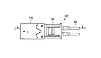
図1は、実施の形態に係る光デバイスおよびコネクタ付光ファイバケーブルの分解図である。図2は、実施の形態に係る光デバイスとコネクタ付光ファイバケーブルとの接続体の模式的な斜視図である。図3は、図2の接続体の模式的な平面図である。図4は、図2の接続体の模式的な側面図である。
(Embodiment)
FIG. 1 is an exploded view of an optical device and an optical fiber cable with a connector according to an embodiment. FIG. 2 is a schematic perspective view of a connection body between the optical device and the connector-attached optical fiber cable according to the embodiment. FIG. 3 is a schematic plan view of the connection body of FIG. 4 is a schematic side view of the connection body of FIG.
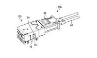
図1〜図4に示すように、光デバイス100は、メス型光コネクタハウジング10と、レンズアセンブリ21、22と、光素子31、32と、スペーサ40と、シールドケース50とを備えており、基板Pに取り付けられるものである。コネクタ付光ファイバケーブル200は、フェルール70が光ファイバケーブル60に取り付けられ、さらにフェルール70がオス型光コネクタ90に取り付けられて構成されている。
As shown in FIGS. 1 to 4, the
このような光デバイス100は、たとえばFOT(Fiber Optical Transceiver)と呼ばれるものであり、車載通信システムにおいて、通信を行う装置に搭載され、コネクタ付光ファイバケーブル200を介して装置間で相互に制御信号等の通信を行う場合に使用される。
Such an
つぎに、コネクタ付光ファイバケーブル200の各構成要素を説明する。
光ファイバケーブル60は、光ファイバ61aと、光ファイバ61aを被覆する素線被覆部61bとからなる光ファイバ素線61と、光ファイバ素線61の外周に長手方向に沿って配置された抗張力体62と、抗張力体62の外周を長手方向に沿って覆う外被覆部63とを備えている。抗張力体62は、たとえばケブラー(登録商標)等のアラミド樹脂繊維からなる。また、素線被覆部61bはたとえばポリアミド樹脂からなる。そして、光ファイバケーブル60の先端で素線被覆部61bと外被覆部63とが一部除去され、光ファイバ61a、素線被覆部61b、および抗張力体62がそれぞれ所定の長さだけ外部に露出するようになっている。
Next, each component of the optical fiber cable with
The
光ファイバ61aは、石英系ガラスからなるコア部とコア部よりも屈折率が低い硬質プラスチックからなるクラッド部とからなる、いわゆるHCS(Hard Clad Silica)光ファイバである。コア部のコア径はたとえば200μm、クラッド部のクラッド径はたとえば230μmであり、850nmの光信号を低損失、広帯域で伝送し、かつ低曲げ損失であり、繰り返しの曲げ、引っ張り動作にも強いように設計されている。
The
フェルール70は、全体的に円筒形状を有している。フェルール70はたとえば耐熱性、機械強度、成型性に優れるポリフェニレンサルファイド樹脂(PPS)からなる。フェルール70には、光ファイバケーブル60が、光ファイバ61aの先端面がフェルール70の先端面71と略一致するように挿通されている。そして、樋形状の光ファイバ固定部材73が、フェルール70の側面部に形成された開口孔72に挿入固定された状態で、光ファイバケーブル60の素線被覆部61bの部分を把持する。これによって、フェルール70は光ファイバケーブル60に固定されている。
The
かしめリング80は、フェルール70と光ファイバケーブル60の外被覆部63とをかしめ、フェルール70と光ファイバケーブル60とを強固に固定している。また、抗張力体62はかしめリング80によってフェルール70の後端部に固定されている。これによって、フェルール70と光ファイバケーブル60とは一体化してより強固になり、振動や衝撃に強くなる。
The
また、かしめリング80の後端部には保護ブーツ82がかぶせられる。保護ブーツ82は、たとえばゴムや弾性を有するプラスチックからなるものであり、フェルール70と光ファイバケーブル60との接続部が許容半径よりも小さい曲げ径で折れ曲がるのを防止しており、これによって光ファイバ素線61が折損することを防止している。
A
オス型光コネクタ90は、2芯構造の光ファイバケーブル60の各先端に取り付けられた2つのフェルール70が挿通されるハウジング91と、フェルール70をハウジング91に固定するための固定部材92とを有している。固定部材92はハウジング91の下部に設けられたスリットに挿入される。ハウジング91はたとえばPPS、ポリブチレンテレフタレート(PBT)からなる。また、車内での利用を考慮すると耐熱性で熱膨張率の小さい樹脂が好ましい。
The male
つぎに、光デバイス100の構成を説明する。
メス型光コネクタハウジング10は、オス型光コネクタ90が挿入され収容される第1収容部11と、レンズアセンブリ21、22、光素子31、32、およびスペーサ40が収容される第2収容部12とを備えている。第2収容部12の側面には、切欠部12a、12b、12cが形成されている。また、メス型光コネクタハウジング10は、基板Pの孔P1に挿入される2本の突起部13と、シールドケース50を安定して固定するための溝部14a、14b、突起部15、および爪係合孔16を備えている。
Next, the configuration of the
The female
つぎに、シールドケース50について具体的に説明する。図5は、シールドケース50の構造を示す模式図である。図5(a)は正面図、図5(b)は右側面図、図5(c)は背面図、図5(d)は平面図、図5(e)は底面図である。なお、シールドケース50の左側面図は右側面図と対称である。また、図6は、図5のA−A線断面図である。図7は、図5のB−B線断面図である。
Next, the
シールドケース50は、導電性があり、かつなるべくインピーダンスが低い材料で構成することが好ましく、たとえば銅材であれば低コストで好ましい。かかる材料として、具体的には、黄銅材(たとえばC2600−1/2H)を使用できる。シールドケース50は、メス型光コネクタハウジング10に被せて光素子31、32をシールドできるように、底面側と背面側とが開放された直方体型の形状を有している。シールドケース50の正面部には、該正面部を構成する板材に切り込みを入れて形成され、かつシールドケース50の内部に向けて突出する突出部51aが形成された板バネ部51と、底面側から下方に向けて延伸する6本の端子部52とが形成されている。左右の側面部のそれぞれには、底面側から下方に向けて延伸する端子部52および係止部53と、切欠部54とが形成されている。上面部を構成する板材の背面側には、底面側に突出している係止爪55が形成されている。また、シールドケース50の内部側には、上面側から底面側へ向かって延伸する板状の嵌合部56、57が形成されている。なお、端子部52は電磁波のシールドのためにグラウンドに接続される端子である。
The
図8は、図5に示すシールドケース50の展開図である。図8に示すように、シールドケース50は、1枚の板材から所定の形状の部材を切り抜き、この部材を折り曲げることによって製造することができる。この板材の厚さは、光デバイス100やシールドケース50の大きさ、あるいはこれらのフットプリントなどに依存するが、成形性や取り扱い易さの点から、0.5mm以上の厚さであることが好ましい。
FIG. 8 is a development view of the
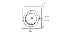
つぎに、レンズアセンブリ21、22と、光素子31、32とについて説明する。図9は、光素子31の模式的な斜視図である。図10は、光素子31、32とレンズアセンブリ21、22との接続を説明する図である。
Next, the
光素子31は、樹脂等からなる筐体31aと、筐体31aから突出し、内周にねじ溝が形成された円管状部31bと、円管状部31b内に配置され発光素子31cと、端子部31dとを備えている。
The
発光素子31cは、たとえば面発光レーザ素子である。発光素子31cは、端子部31dから、筐体31aに収容された配線を介して電力および電気信号が供給され、通信用光信号を出力する。
The
光素子32は、光素子31において、発光素子31cを受光素子に置き換えた構成を有する。受光素子は、たとえばフォトダイオードである。この受光素子は、端子部32dから、筐体32aに収容された配線を介して逆バイアス電圧が印加され、通信用光信号を受光してこれを電気信号に変換して、この電気信号を端子部32dから出力する。
The
レンズアセンブリ21は、集光レンズ21aと、集光レンズ21aを保持する筐体21bとを備えている。筐体21bには、フランジ部21baと、外周にねじ溝が形成されたねじ部21bbと、フランジ部21baに形成された突起部21bc、21bdとが形成されている。
The
レンズアセンブリ22は、集光レンズ22aと、集光レンズ22aを保持する筐体22bとを備えている。筐体22bには、フランジ部22baと、外周にねじ溝が形成されたねじ部22bbと、フランジ部22baに形成された突起部22bc、22bdとが形成されている。
The
図1に戻って、スペーサ40は、シールドケース50の板バネ部51と光素子31、32との間に介挿され、光素子31、32を安定して固定するためのものである。スペーサ40の側面には、上述した第2収容部12の切欠部12a、12b、12cに嵌合する突起部41、42、43が形成されている。スペーサ40は、たとえばPPS、PBTからなる。また、車内での利用を考慮すると耐熱性で熱膨張率の小さい樹脂が好ましい。なお、スペーサ40は、機械的負荷が小さいため、フィラーが配合されていないPBTからなるものでもよい。
Returning to FIG. 1, the
つぎに、光デバイス100の組立方法について説明する。
まず、光素子31の円管状部31bにレンズアセンブリ21のねじ部21bbをねじ込んで組立てる。これによって、光素子31とレンズアセンブリ21とは強固に固定される。また、光素子31とレンズアセンブリ21とを接着剤によって接合するよりも、接着剤が固化するのに要する時間を削減できるので、作業時間が短縮される。また、レンズアセンブリ21をねじ込んだときに、フランジ部21baと円管状部31bとが当接するため、その当接した位置で発光素子31cと集光レンズ21aとの距離が固定される。したがって、たとえば組立作業者の技量によらず、発光素子31cと集光レンズ21aとの距離が安定した組立が実現される。なお、光素子32とレンズアセンブリ22とについても、同様にして組立を行う。
Next, a method for assembling the
First, the threaded portion 21bb of the
また、図10に示すように、レンズアセンブリ21における突起部21bc、21bdは、フランジ部21baの円周方向において180度の角度をなすように配置されている。これに対して、レンズアセンブリ22における突起部22bc、22bdは、フランジ部22baの円周方向において90度の角度をなすように配置されている。レンズアセンブリ21とレンズアセンブリ22とはこの突起部のなす角度の違いによって区別することができるので、組立時に、たとえばレンズアセンブリ21を光素子32に取り付けるといった取り違えを防止することができる。
Further, as shown in FIG. 10, the protrusions 21bc and 21bd in the
つぎに、組み立てた光素子31とレンズアセンブリ21、および光素子32とレンズアセンブリ22とを、メス型光コネクタハウジング10の第2収容部12に収容する。
Next, the assembled
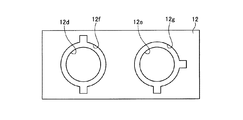
ここで、図11は、メス型光コネクタハウジング10の第2収容部12をレンズアセンブリ21、22側からみた模式図である。図11に示すように、第2収容部12には、レンズアセンブリ21、22が挿入される挿入孔12d、12eが形成されている。さらに、挿入孔12d、12eの周囲には、溝部12f、12gが形成されている。溝部12fの形状は、レンズアセンブリ21のフランジ部21baと、突起部21bc、21bdとが嵌合するような形状に形成されている。溝部12gの形状は、レンズアセンブリ22のフランジ部22baと、突起部22bc、22bdとが嵌合するような形状に形成されている。これによって、組立時に、たとえばレンズアセンブリ21と光素子31とを挿入孔12e側に取り付けるといった取り違えを防止することができる。
Here, FIG. 11 is a schematic view of the
つぎに、光素子31、32の後部からスペーサ40を第2収容部12に収容する。このとき、スペーサ40の側面に形成された突起部41、42、43が、第2収容部12に形成された切欠部12a、12b、12cに嵌合する。これによって、スペーサ40は第2収容部12に安定して収容される。切欠部12a、12b、12cおよび突起部41、42、43は嵌合する方向に長さを有するので、スペーサ40が第2収容部12に収容される際に、傾いて収容されことが防止される。また、突起部41と、突起部42、43とは、左右非対称に配置されているため、スペーサ40が上下逆に収容されるおそれもない。
Next, the
つぎに、光素子31、32、およびスペーサ40を収容したメス型光コネクタハウジング10にシールドケース50を取り付ける。このとき、シールドケース50の嵌合部56、57が、メス型光コネクタハウジング10の溝部14a、14bにそれぞれ嵌合する。また、シールドケース50の係止爪55が、メス型光コネクタハウジング10の爪係合孔16に係合する。さらに、シールドケース50の切欠部54には、メス型光コネクタハウジング10の突起部15が嵌合する(図2、4参照)。これによって、シールドケース50は、車両の走行時の振動、衝撃等に対しても耐えうるように、メス型光コネクタハウジング10に強固に安定して固定される。
Next, the
また、シールドケース50がメス型光コネクタハウジング10に取り付けられた状態で、板バネ部51がスペーサ40を介して光素子31、32とレンズアセンブリ21、22とを押圧し、メス型光コネクタハウジング10に押付けている。これによって、光素子31、32とレンズアセンブリ21、22とは、車両の走行時の振動、衝撃等に対しても耐えうるように、メス型光コネクタハウジング10に強固に安定して固定される。なお、溝部12f、12gが、レンズアセンブリ21、22の各フランジ部21ba、22baおよび突起部が嵌合するような形状に形成されている構成も、上記の安定した固定に寄与している。
Further, in a state where the
また、シールドケース50はメス型光コネクタハウジング10に強固に安定して固定されるので、板バネ部51の光素子31、32とレンズアセンブリ21、22とに対する押圧力も安定する。
Since the
また、板バネ部51がスペーサ40を介して光素子31、32とレンズアセンブリ21、22とを押圧しているので、板バネ部51の押圧力を光素子31、32の一箇所に集中させず、面的に均一に掛けることができる。また、スペーサ40は、金属製の板バネ部51よりも柔らかい材料からなるので、板バネ部51の押圧力が光素子31、32の樹脂等からなる筐体に直接掛からないためのクッションとしても機能する。これによって、発光素子や受光素子に余計な応力が掛かってその光学特性が劣化することが防止される。また、スペーサ40は、傾斜せずに第2収容部12に収容されるので、スペーサ40を介した押圧力が光素子31、32に対して傾斜して掛かることも防止される。
Further, since the
ここで、光素子31、32等をメス型光コネクタハウジング10に押付けるバネ構造を、たとえはスペーサ等と同じ樹脂材料で構成したとすると、車両内が高温になった場合に、バネ弾性が低下する場合があるので、当初の押圧力を維持できないおそれがある。
Here, assuming that the spring structure for pressing the
これに対して、本実施の形態では、電磁波をシールドすべき金属からなるシールドケース50に板バネ部51を設けているので、高温化でもバネ弾性の低下が発生せず、安定した固定状態を維持できる。また、新たに金属からなるバネ部材を追加する構成ではないので、部品点数の増加も防止される。
In contrast, in the present embodiment, since the
つぎに、このように組み立てられた光デバイス100を、基板Pに取り付ける(図1、4参照)。基板Pに取り付ける際には、メス型光コネクタハウジング10の突起部13が孔P1に挿入される。光素子31、32の合計10本の端子部31d、32dが孔P2に挿入される。シールドケース50の合計8本の端子部52は孔P3に挿入される。シールドケース50の2本の係止部53は孔P4に挿入される。
Next, the
係止部53は、孔P4に挿入されて係止される。これによって、光デバイス100は基板Pに対して位置決めされる。その後、端子部31d、32d、端子部52は電気的導通のために基板Pに半田付けされるが、光デバイス100は係止部53によって基板Pへの各端子の挿入深さも位置決めされるので、半田付けの際に光デバイス100が基板Pに対して浮き上がったり、傾いたりすることが防止される。
The locking
また、光デバイス100が係止部53によって基板Pに固定されるため、光デバイス100に振動、衝撃等による力が加えられた場合、係止部53もその力を負担するため、端子部31d、32d、端子部52への負荷が軽減される。これによって、端子部31d、32d、端子部52の電気的導通のための半田に掛かる負荷も軽減される。
Further, since the
その後、この光デバイス100にコネクタ付光ファイバケーブル200を接続することによって、所望の光通信を実行することができる。
Thereafter, by connecting the optical fiber cable with
なお、図12は、図3のC−C線断面図である。図13は、図4のD−D線断面図である。図12、図13に示すように、板バネ部51はスペーサ40を介して光素子31、32とレンズアセンブリ21、22とを押圧し、メス型光コネクタハウジング10に押付けている。また、スペーサ40の突起部41が、第2収容部12に形成された切欠部12aに嵌合している。また、シールドケース50の嵌合部56、57が、メス型光コネクタハウジング10の溝部14a、14bにそれぞれ嵌合している。また、たとえば溝部12fには、レンズアセンブリ21のフランジ部21baと、突起部21bc、21bdとが嵌合している。
12 is a cross-sectional view taken along the line CC of FIG. 13 is a cross-sectional view taken along the line DD of FIG. As shown in FIGS. 12 and 13, the
(シールドケースの変形例)
本発明に係るシールドケースは図5に示すものに限られない。図14は、シールドケースの変形例であるシールドケース50Aの構造を示す模式図である。図14(a)は正面図、図14(b)は右側面図、図14(c)は背面図、図14(d)は平面図、図14(e)は底面図である。なお、シールドケース50Aの左側面図は右側面図と対称である。
(Modification of shield case)
The shield case according to the present invention is not limited to that shown in FIG. FIG. 14 is a schematic diagram showing the structure of a
図14に示すように、シールドケース50Aは、シールドケース50と同様に、メス型光コネクタハウジング10に被せて光素子31、32をシールドできるように底面側と背面側とが開放された直方体型の形状を有している。シールドケース50Aは、導電性があり、かつなるべくインピーダンスが低い材料で構成することが好ましく、たとえば銅材であれば低コストで好ましい。かかる材料として、具体的には、黄銅材(たとえばC2600−1/2H)を使用できる。また、シールドケース50Aには、突出部51aが形成された板バネ部51と、合計8本の端子部52と、係止部53と、切欠部54と、嵌合部56、57とが形成されている。ただし、シールドケース50Aには上面部に係止爪が形成されていない。このような係止爪を備えていないシールドケース50Aであっても、シールドケース50と同様の効果を奏するものとなる。
図15は、図14に示すシールドケース50Aの展開図である。図15に示すように、シールドケース50Aは、1枚の板材から所定の形状の部材を切り抜き、この部材を折り曲げることによって製造することができる。
As shown in FIG. 14, similarly to the
FIG. 15 is a development view of the
なお、上記実施の形態では、2芯の光ファイバケーブルを用いており、光デバイスは光信号の送受信を行うものであるが、本発明はこれに限らず、1芯または3芯以上の多芯の光ファイバケーブルを用いて、光信号の送信のみ、受信のみ、または送受信を行う光デバイスに適用してもよい。 In the above-described embodiment, a two-core optical fiber cable is used, and the optical device transmits and receives an optical signal. However, the present invention is not limited to this, and the one-core or three-core or more multi-core is used. The optical fiber cable may be applied to an optical device that performs only transmission, reception, or transmission / reception of optical signals.
なお、上記実施の形態では、光デバイスが備える光コネクタハウジングはメス型であるが、オス型の光コネクタハウジングを用いてもよい。 In the above embodiment, the optical connector housing included in the optical device is a female type, but a male type optical connector housing may be used.
また、上記実施の形態により本発明が限定されるものではない。上述した各構成要素を適宜組み合わせて構成したものも本発明に含まれる。その他、上記実施の形態に基づいて当業者等によりなされる他の実施の形態、実施例及び運用技術等は全て本発明に含まれる。 Further, the present invention is not limited by the above embodiment. What was comprised combining each component mentioned above suitably is also contained in this invention. In addition, other embodiments, examples, operational techniques, and the like made by those skilled in the art based on the above-described embodiments are all included in the present invention.
10 メス型光コネクタハウジング
11 第1収容部
12 第2収容部
12a、12b、12c 切欠部
12d、12e 挿入孔
12f、12g、14a、14b 溝部
13、15、21bc、21bd、22bc、22bd、41、42、43 突起部
16 爪係合孔
21、22 レンズアセンブリ
21a、22a 集光レンズ
21b、22b、31a、32a 筐体
21ba、22ba フランジ部
21bb、22bb ねじ部
31、32 光素子
31b、32b 円管状部
31c 発光素子
31d、32d 端子部
40 スペーサ
50、50A シールドケース
51 板バネ部
51a 突出部
52 端子部
53 係止部
54 切欠部
55 係止爪
56、57 嵌合部
60 光ファイバケーブル
61 光ファイバ素線
61a 光ファイバ
61b 素線被覆部
62 抗張力体
63 外被覆部
70 フェルール
71 先端面
72 開口孔
73 光ファイバ固定部材
80 かしめリング
82 保護ブーツ
90 オス型光コネクタ
91 ハウジング
92 固定部材
100 光デバイス
200 コネクタ付光ファイバケーブル
P 基板
P1、P2、P3、P4 孔
DESCRIPTION OF
Claims (16)
当該シールドケースの正面部に、該正面部を構成する板材に切り込みを入れて形成された、当該シールドケースを前記光コネクタハウジングに被せたときに前記光素子を押圧する板バネ部が形成されていることを特徴とするシールドケース。 The bottom side and the back side have a shape that is open, and is a metal shield case that covers an optical connector housing that houses an optical element,
A plate spring portion is formed in the front portion of the shield case, which is formed by cutting the plate material constituting the front portion, and presses the optical element when the shield case is put on the optical connector housing. Shield case characterized by
光素子を収容する収容部を有する光コネクタハウジングと、
底面側と背面側とが開放された形状を有し、前記光コネクタハウジングに被せられる金属製のシールドケースであって、当該シールドケースの正面部に、該正面部を構成する板材に切り込みを入れて形成された、当該シールドケースを前記光コネクタハウジングに被せたときに前記光素子を押圧する板バネ部が形成されているシールドケースと、
を備えることを特徴とする光デバイス。 An optical element;
An optical connector housing having an accommodating portion for accommodating an optical element;
A metal shield case having a shape in which a bottom surface side and a back surface side are opened, and is covered with the optical connector housing, and a cut is made in a front plate of the shield case at a front surface portion of the shield case. A shield case formed with a leaf spring portion that presses the optical element when the shield case is put on the optical connector housing; and
An optical device comprising:
前記シールドケースは、当該シールドケースを前記光コネクタハウジングに被せたときに、前記溝部に嵌合する板状の嵌合部が形成されていることを特徴とする請求項8〜12のいずれか一つに記載の光デバイス。 The optical connector housing has a groove,
The said shield case is formed with the plate-shaped fitting part fitted to the said groove part when the said shield case is covered on the said optical connector housing, The any one of Claims 8-12 characterized by the above-mentioned. Optical device as described in one.
前記シールドケースは、当該シールドケースを前記光コネクタハウジングに被せたときに、前記第1突起部と嵌合する第1切欠部が形成されていることを特徴とする請求項8〜13のいずれか一つに記載の光デバイス。 The optical connector housing has a first protrusion,
14. The shield case is formed with a first notch that fits with the first protrusion when the shield case is put on the optical connector housing. The optical device according to one.
前記スペーサは前記第2切欠部に嵌合する第2突起部を有することを特徴とする請求項15に記載の光デバイス。 The housing part of the optical connector housing has a second notch,
The optical device according to claim 15, wherein the spacer has a second protrusion that fits into the second notch.
Priority Applications (1)
| Application Number | Priority Date | Filing Date | Title |
|---|---|---|---|
| JP2011119188A JP2012247621A (en) | 2011-05-27 | 2011-05-27 | Shield case and optical device |
Applications Claiming Priority (1)
| Application Number | Priority Date | Filing Date | Title |
|---|---|---|---|
| JP2011119188A JP2012247621A (en) | 2011-05-27 | 2011-05-27 | Shield case and optical device |
Publications (1)
| Publication Number | Publication Date |
|---|---|
| JP2012247621A true JP2012247621A (en) | 2012-12-13 |
Family
ID=47468108
Family Applications (1)
| Application Number | Title | Priority Date | Filing Date |
|---|---|---|---|
| JP2011119188A Pending JP2012247621A (en) | 2011-05-27 | 2011-05-27 | Shield case and optical device |
Country Status (1)
| Country | Link |
|---|---|
| JP (1) | JP2012247621A (en) |
Cited By (1)
| Publication number | Priority date | Publication date | Assignee | Title |
|---|---|---|---|---|
| WO2013146697A1 (en) * | 2012-03-30 | 2013-10-03 | 古河電気工業株式会社 | Optical connector, housing for optical connector, and metal case for optical connector |
Citations (11)
| Publication number | Priority date | Publication date | Assignee | Title |
|---|---|---|---|---|
| JPH01177714U (en) * | 1988-06-02 | 1989-12-19 | ||
| JPH07181352A (en) * | 1993-12-24 | 1995-07-21 | Babcock Hitachi Kk | Optical element module |
| JP2002190344A (en) * | 2000-12-20 | 2002-07-05 | Furukawa Electric Co Ltd:The | Optoelectronic composite connector |
| JP2006215276A (en) * | 2005-02-03 | 2006-08-17 | Yazaki Corp | Optical connector |
| JP2006236936A (en) * | 2005-02-28 | 2006-09-07 | Mitsumi Electric Co Ltd | Connector lock device for module |
| US20070297745A1 (en) * | 2006-06-21 | 2007-12-27 | Thomas Moriarty | Optical connector |
| JP2009075396A (en) * | 2007-09-21 | 2009-04-09 | Panasonic Electric Works Co Ltd | Optical connector |
| JP2010175575A (en) * | 2009-01-27 | 2010-08-12 | Yazaki Corp | Optical connector |
| JP2010181523A (en) * | 2009-02-04 | 2010-08-19 | Yazaki Corp | Optical connector |
| JP2011028851A (en) * | 2009-07-21 | 2011-02-10 | Yazaki Corp | Shield case and connector with connector housing shielded by the same |
| JP2011100033A (en) * | 2009-11-09 | 2011-05-19 | Alps Electric Co Ltd | Optical connector |
-
2011
- 2011-05-27 JP JP2011119188A patent/JP2012247621A/en active Pending
Patent Citations (11)
| Publication number | Priority date | Publication date | Assignee | Title |
|---|---|---|---|---|
| JPH01177714U (en) * | 1988-06-02 | 1989-12-19 | ||
| JPH07181352A (en) * | 1993-12-24 | 1995-07-21 | Babcock Hitachi Kk | Optical element module |
| JP2002190344A (en) * | 2000-12-20 | 2002-07-05 | Furukawa Electric Co Ltd:The | Optoelectronic composite connector |
| JP2006215276A (en) * | 2005-02-03 | 2006-08-17 | Yazaki Corp | Optical connector |
| JP2006236936A (en) * | 2005-02-28 | 2006-09-07 | Mitsumi Electric Co Ltd | Connector lock device for module |
| US20070297745A1 (en) * | 2006-06-21 | 2007-12-27 | Thomas Moriarty | Optical connector |
| JP2009075396A (en) * | 2007-09-21 | 2009-04-09 | Panasonic Electric Works Co Ltd | Optical connector |
| JP2010175575A (en) * | 2009-01-27 | 2010-08-12 | Yazaki Corp | Optical connector |
| JP2010181523A (en) * | 2009-02-04 | 2010-08-19 | Yazaki Corp | Optical connector |
| JP2011028851A (en) * | 2009-07-21 | 2011-02-10 | Yazaki Corp | Shield case and connector with connector housing shielded by the same |
| JP2011100033A (en) * | 2009-11-09 | 2011-05-19 | Alps Electric Co Ltd | Optical connector |
Cited By (1)
| Publication number | Priority date | Publication date | Assignee | Title |
|---|---|---|---|---|
| WO2013146697A1 (en) * | 2012-03-30 | 2013-10-03 | 古河電気工業株式会社 | Optical connector, housing for optical connector, and metal case for optical connector |
Similar Documents
| Publication | Publication Date | Title |
|---|---|---|
| US6783283B2 (en) | Optical connector for coupling optical signals to optical devices | |
| US8737784B2 (en) | Optical communication module and optical communication connector | |
| US9182551B2 (en) | Lens component and optical module provided with the same | |
| US9964714B2 (en) | Optical connector | |
| US8491197B2 (en) | Optical connector module | |
| US8905649B2 (en) | Optical fiber terminal fixing member, optical connector, and optical fiber cable with connector | |
| JP2012194481A (en) | Optical connector, method for mounting optical fiber, and electronic information device | |
| US10261269B2 (en) | Optical module | |
| JP2012088571A (en) | Optoelectric composite connector and cable with connector | |
| WO2010007861A1 (en) | Optical connector | |
| JP2007241105A (en) | Connector | |
| US20130170798A1 (en) | Optical fiber terminal, optical fiber cable with terminal, optical connector, optical fiber cable with connector, and connection structure | |
| US20080292250A1 (en) | Optical communication module and optical communication module holder | |
| WO2014185260A1 (en) | Optical connector | |
| JP2008152060A (en) | Optical path conversion-type optical connector and circuit board using the same | |
| JP2012247622A (en) | Optical element assembly and optical device | |
| JP5543293B2 (en) | Small-diameter bending optical connector | |
| JP5460554B2 (en) | Photoelectric composite connector and cable with connector | |
| JP2015500517A (en) | Optical module | |
| US11656415B2 (en) | Optical connector cable | |
| JP2012247621A (en) | Shield case and optical device | |
| US8246257B2 (en) | Optical fiber connector | |
| JP5375535B2 (en) | Photoelectric conversion module | |
| JP2013011692A (en) | Connector and lock structure of connector | |
| US20230204880A1 (en) | Connector member, optical transmission system, and assembly method for same |
Legal Events
| Date | Code | Title | Description |
|---|---|---|---|
| A621 | Written request for application examination |
Free format text: JAPANESE INTERMEDIATE CODE: A621 Effective date: 20140304 |
|
| A977 | Report on retrieval |
Free format text: JAPANESE INTERMEDIATE CODE: A971007 Effective date: 20141128 |
|
| A131 | Notification of reasons for refusal |
Free format text: JAPANESE INTERMEDIATE CODE: A131 Effective date: 20141216 |
|
| A02 | Decision of refusal |
Free format text: JAPANESE INTERMEDIATE CODE: A02 Effective date: 20150414 |