JP2012244521A - Comparator and ad converter - Google Patents
Comparator and ad converter Download PDFInfo
- Publication number
- JP2012244521A JP2012244521A JP2011114534A JP2011114534A JP2012244521A JP 2012244521 A JP2012244521 A JP 2012244521A JP 2011114534 A JP2011114534 A JP 2011114534A JP 2011114534 A JP2011114534 A JP 2011114534A JP 2012244521 A JP2012244521 A JP 2012244521A
- Authority
- JP
- Japan
- Prior art keywords
- comparator
- output
- signal
- input
- comparison
- Prior art date
- Legal status (The legal status is an assumption and is not a legal conclusion. Google has not performed a legal analysis and makes no representation as to the accuracy of the status listed.)
- Withdrawn
Links
Images


Abstract
Description
本発明は、比較器及びこれを有するAD変換器に関する。 The present invention relates to a comparator and an AD converter having the same.
従来から、アナログデジタル(AD:Analog Digital)変換器等(以下「ADC」と言う。)に用いられる種々の比較器(コンパレータ)が開発され、提案されている。特許文献1は、比較器の判定時間を改善するために、比較器を2段構成としてメタステーブル状態(未判定状態)である時間を短縮し高速化する技術を開示している。また、特許文献2は、異なる比較値を持つ2つのコンパレータを有し、この2つのコンパレータのうち、先に出力したコンパレータの判定信号を採用する技術を開示している。
Conventionally, various comparators (comparators) used for analog-digital (AD) converters (hereinafter referred to as “ADC”) have been developed and proposed.
これらの従来技術からも明らかなように、一般に、比較器は、比較すべき信号が入力されてから、信頼できる比較結果が出力されるまでに、精度に応じた一定の遅延時間を要する。現在においては、AD変換器等、高速で動作することが必要とされる多くの機器に比較器が用いられているため、比較器の動作速度の改善が望まれている。 As is clear from these prior arts, in general, a comparator requires a certain delay time depending on accuracy until a reliable comparison result is output after a signal to be compared is input. At present, comparators are used in many devices that are required to operate at high speed, such as AD converters, and therefore it is desired to improve the operation speed of the comparators.
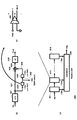
ここで、図1を参照し、従来のクロック同期型比較器100の動作について説明する。(クロック同期型比較器とは、クロック信号がハイ(ロウ)のときに比較動作を行い、ロウ(ハイ)のときはハイ、もしくはロウのうちどちらかの初期値にリセットが掛かる比較器のことを指す。)比較器100は、入力端子clk及びVin及びVipを有し、出力端子C+及びC−を有する。clkがロウのときはリセットが掛かり、比較器100は初期状態に移行し、それと同時に直前の比較結果を保持する。clkがハイになると比較動作を開始しVinとVipの極性を判定する。例えば、Vinの電圧がVipの電圧よりも低ければ、出力端子C+は、ハイレベルの信号が出力される。また、Vinの電圧がVipの電圧よりも高ければ、出力端子C+には、ロウレベルの信号が出力される。なお、出力端子C−は、出力端子C+の反転した信号が出力される。
Here, the operation of the conventional clock
clkがハイになると入力信号Vin及びVipは、差動増幅回路110に入力され、対応する出力信号cp及びcnが出力される。cp及びcnは、それぞれNOT回路121及び122を介して、それぞれデジタル信号IP及びINとなる。信号IP及びINは、たすきがけに接続されたNOR回路131及び132で構成されるSR(Set Reset)ラッチ回路でラッチされる。このラッチされた信号が、比較器100の出力信号C+及びC−として取り出され、clkがロウの間は直前の比較結果を保持する。なお、本明細書では、Vinを負極入力、Vipを正極入力として扱うのでVin<Vipで比較器出力がハイレベルを出力しているが、この逆であってもよい。
When clk goes high, the input signals Vin and Vip are input to the
図2は、図1における差動増幅回路110の具体的回路の一例を示した図である。VDDは電源ライン、GNDはグランドを示す。図2に示されるように、トランジスタ210乃至220が接続されており、クロック信号clkの立ち上がりのタイミングで動作を開始し、立ち下がりのタイミングでリセットされる。トランジスタ210、211、218及び219のそれぞれのゲート端子には、クロック信号が入力され、ロウになると差動増幅回路をリセットする。トランジスタ220のゲート端子にもクロック信号が入力されており、クロックの立ち上がりタイミングで差動増幅回路110が動作を開始する。本実施例の場合、トランジスタ210、211、218及び219はpMOSトランジスタであり、トランジスタ220はnMOSトランジスタである。したがって、同じクロック信号が入力された場合でも、トランジスタ210、211、218及び219とトランジスタ220のオン/オフ動作は、逆になっている。すなわち、clkがロウ(L)のとき、nMOSトランジスタ220はオフとなり差動増幅回路110の動作は停止し、また、このとき、トランジスタ210、211、218及び219はオンとなり、差動増幅回路110はリセットされる。clkがハイ(H)のときは、トランジスタ210、211、218及び219はオフとなり、差動増幅回路110はリセット状態が解除されて入力信号を受け付けるようになり、また、このとき、nMOSトランジスタ220はオンとなり差動増幅回路110が動作を開始する。
FIG. 2 is a diagram showing an example of a specific circuit of the
トランジスタ217及び216のゲート端子には、それぞれ入力信号Vin及びVipが入力される。トランジスタ212乃至215によって、入力信号Vin及びVipが差動増幅され、cp及びcnとして出力される。
Input signals Vin and Vip are input to the gate terminals of the
なお、この動作は、一例であり、クロック信号入力に同期する比較器(前述のクロック同期型比較器)であれば、本発明を適用することが出来る。 This operation is an example, and the present invention can be applied to any comparator that is synchronized with the clock signal input (the above-mentioned clock synchronous comparator).
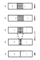
図3(a)乃至(c)は、図2における差動増幅回路110の出力cp及びcnの挙動を示した図である。また、図3(d)乃至(f)は、それぞれ対応するクロック信号clkの波形を示している。
3A to 3C are diagrams showing the behavior of the outputs cp and cn of the
図3(a)は、入力信号VinとVipとの差の絶対値|ΔVin|が比較的大きい場合における出力cp及びcnの挙動を示している。出力cp及びcnは、クロック信号(d)の立ち上がり時点では、直前のリセット動作により共にVDDに接続されているため、同じ値を示しているが、次第に差が増幅され、クロック信号(d)の立ち下がり時においては、比較結果を出力するのに十分大きな差が発生している。このようにcpとcnの差が十分大きい場合には、図1に示したラッチ回路131で、信頼できる比較結果が出力されることになる。
FIG. 3A shows the behavior of the outputs cp and cn when the absolute value | ΔVin | of the difference between the input signals Vin and Vip is relatively large. The outputs cp and cn are both connected to VDD at the time of rising of the clock signal (d) because they are both connected to VDD by the immediately preceding reset operation. However, the difference is gradually amplified and the clock signal (d) At the time of falling, a sufficiently large difference is generated to output the comparison result. In this way, when the difference between cp and cn is sufficiently large, the
図3(b)は、入力信号VinとVipとの差の絶対値|ΔVin|が、図3(a)と比較して小さい場合における出力cp及びcnの挙動を示している。この場合には、出力cp及びcnの電圧差が十分な値まで増幅されるのに必要な時間が、図3(a)の場合に比べて相対的に長くなる。したがって、クロック(e)の立ち下がり時点においても、出力cp及びcnの差が小さいため、後段のラッチ回路131に比較結果を反映できず、前回の判定結果がそのまま用いられる。このため、比較器100が誤った判定結果を出力することが比較的高い確率で発生してしまうことになる。
FIG. 3B shows the behavior of the outputs cp and cn when the absolute value | ΔVin | of the difference between the input signals Vin and Vip is smaller than that in FIG. In this case, the time required for the voltage difference between the outputs cp and cn to be amplified to a sufficient value is relatively longer than in the case of FIG. Therefore, the difference between the outputs cp and cn is small even when the clock (e) falls, so that the comparison result cannot be reflected in the
図3(c)は、図3(b)における誤動作を回避するために、クロック信号(f)を遅くするか、クロックのデューティー比を長くすることによって、比較時間を長く設定した例を示している。この場合には、クロック信号(f)の立ち下がり時において、出力cpとcnとの電圧差が十分大きくなっているため、後段のラッチ回路131の書き換えが正常に行われ誤動作の発生を防止できる。
FIG. 3 (c) shows an example in which the comparison time is set longer by slowing down the clock signal (f) or increasing the duty ratio of the clock in order to avoid the malfunction in FIG. 3 (b). Yes. In this case, when the clock signal (f) falls, the voltage difference between the outputs cp and cn is sufficiently large, so that the
このように、図3に示す例から理解できるように、入力信号VinとVipとの差の絶対値|ΔVin|が小さい場合には、比較器における比較結果が得られる時間が長くかかることになる。このことを、別の言葉で言い換えれば、比較結果が未判定である状態が長くなると言うことである。この比較が未判定である状態を、メタステーブル状態と呼ぶ。 In this way, as can be understood from the example shown in FIG. 3, when the absolute value | ΔVin | of the difference between the input signals Vin and Vip is small, it takes a long time to obtain a comparison result in the comparator. . In other words, this means that the state in which the comparison result is not determined becomes longer. A state in which this comparison is not determined is referred to as a metastable state.
このような、比較時間の増大を避けるために、特許文献1では、比較器を、直列に接続した第1段目比較回路部と第2段目比較回路部の2段構成としている。第1段目比較回路部は、第1のクロックタイミングで動作し、入力信号のレベルと基準レベルとの比較判定結果に応じて、ハイレベルまたはロウレベルの出力電圧を比較出力として出力すると共に、比較判定が終わっていない間は、増幅途中の信号をそのまま出力し第2段目の比較回路部へと入力する。第2段目比較回路部は、第1のクロックタイミングより遅れた第2のクロックタイミングで動作し、第1段目比較回路部の比較出力を、中間レベルの出力電圧とは異なる値の比較用電圧と比較し、その比較判定結果に応じて比較出力を出力すると共に、その判定結果の比較出力を自己保持するようにしている。
In order to avoid such an increase in comparison time, in
また、特許文献2では、比較器回路は,入力信号と第1の比較値とを比較し判定結果を有する第1の判定信号を生成する第1の差動増幅回路部と,入力信号と,第1の比較値と異なる第2の比較値とを比較し判定結果を有する第2の判定信号を生成する第2の差動増幅回路部とを有する。そして、第1及び第2の判定信号のうちいずれが先に生成されたかを検出し,先に生成された信号を選択して判定信号として出力する出力選択回路部とを有する。
In
また、非特許文献1には、比較器を用いたADCの技術が開示されている。この非特許文献1では、比較器において、入力信号の判定が終了し比較結果が得られたという信号を利用した非同期のAD変換技術が開示されている。上述のように、入力信号の差の絶対値である|ΔVin|の大きさによって、比較器における比較動作時間が異なるため、判定が終了したという信号を用いて、入力信号に応じた適切な比較時間をそれぞれの比較動作に割り振ることにより、1回のAD変換に掛かる比較時間の合計を削減しつつ比較結果の信頼性を向上させている。
Non-Patent
しかしながら、上述の特許文献1及び特許文献2に開示されている技術は、比較に要する時間を短縮するために、比較器を複数設けなければならず、比較器全体の回路構成が複雑化している。
However, in the techniques disclosed in
また、非特許文献1に開示される技術においては、比較器の判定にかかる時間の短縮は、あくまでもADCにおける比較の判定時間の平均値の短縮であり、AD変換において複数回必要となる複数の比較動作の各々の時間を短縮するものではない。また、判定時間が長時間になる場合には、一定の値を超えた時点で比較の打ち切りをすることも必要となってくる。比較を打ち切った場合、このときの出力結果は前回の比較結果をそのまま用いることとなり、AD変換そのものの出力精度の低下を招く場合もある。
Further, in the technique disclosed in
したがって、高速で動作する高精度な比較器を実現することが望まれている。 Therefore, it is desired to realize a highly accurate comparator that operates at high speed.
本発明は、上述の従来技術の課題を解決することを目的とする。すなわち、本願発明は、高速で動作する高精度な比較器を実現することを目的とする。また、この比較器を利用して、高速に、かつ高精度で動作するADC等の応用機器を実現することを目的とする。なお、本発明の課題は、上記の点に限定されるものではない。 An object of the present invention is to solve the above-described problems of the prior art. That is, an object of the present invention is to realize a highly accurate comparator that operates at high speed. Another object of the present invention is to realize an applied device such as an ADC that operates at high speed and with high accuracy by using the comparator. In addition, the subject of this invention is not limited to said point.
一実施例の比較器は、クロック信号に同期して第1の入力信号(Vin)及び第2の入力信号(Vip)を比較する比較器(400)であって、当該比較器の内部状態として、ハイレベル状態と(Z1)、ロウレベル状態と(Z5)、前記ハイレベル状態及び前記ロウレベル状態の中間のN(Nは自然数)個のレベル(Z2乃至Z4)を表すN個のミドルレベル状態とを持ち、当該比較器(400)は、前記第1の入力信号(Vin)及び前記第2の入力信号(Vip)が入力され、前記第1の入力信号(Vin)及び前記第2の入力信号(Vip)に対応しかつ増幅された第1の差動増幅信号(IP)及び第2の差動増幅信号(IN)を出力する差動増幅回路部(110、121、122)であって、前記クロック信号の第1のクロックタイミング(clk1の立ち上がり)で動作を開始し前記クロック信号の第2のクロックタイミング(clk1の立ち下がり)で動作を終了する、差動増幅回路部(110、121、122)と、前記第1の差動増幅信号(IP)及び前記第2の差動増幅信号(IN)に基づいて動作し、前記第1の差動増幅信号(IP)及び前記第2の差動増幅信号(IN)を比較した値を第1の比較値(C)としてラッチし出力する第1のラッチ部(Latch)と、前記第1の差動増幅信号(IP)及び前記第2の差動増幅信号(IN)に基づいて動作し、前記第1の差動増幅信号(IP)及び前記第2の差動増幅信号(IN)を比較した値(417)を遅延させたN個の値(遅延可変部413、1713、1714の出力)を第3のクロックタイミング(clk2の立ち上がり)でラッチし第2のN個の比較値(Mout、M1、M2)として出力する、N個のラッチ回路(415、1715、1716)を含む第2のラッチ部(1bitTDC,2bitTDC)と、を有し、前記第1の比較値(C)と前記第2のN個の比較値(Mout、M1、M2)とに基づいて、前記ハイレベル状態と前記ロウレベル状態と前記N個のミドルレベル状態とが決定される、比較器(400、1700)によって提供される。なお、上記の「遅延」は、遅延量=0(例えば、実施例における遅延可変部413が存在しない場合等)を含む点に留意すべきである。
A comparator according to an embodiment is a comparator (400) that compares a first input signal (Vin) and a second input signal (Vip) in synchronization with a clock signal, and that is an internal state of the comparator. A high level state (Z1), a low level state (Z5), and N middle level states representing N (N is a natural number) levels (Z2 to Z4) between the high level state and the low level state. The comparator (400) receives the first input signal (Vin) and the second input signal (Vip), and the first input signal (Vin) and the second input signal. A differential amplifier circuit section (110, 121, 122) corresponding to (Vip) and outputting the amplified first differential amplified signal (IP) and second differential amplified signal (IN), A first clock counter of the clock signal; Differential amplifier circuit section (110, 121, 122) that starts operation at the timing (rise of clk1) and finishes operation at the second clock timing (fall of clk1) of the clock signal, and the first Operates based on the differential amplification signal (IP) and the second differential amplification signal (IN), and compares the first differential amplification signal (IP) and the second differential amplification signal (IN). The first latch portion (Latch) that latches and outputs the value as the first comparison value (C), and the first differential amplification signal (IP) and the second differential amplification signal (IN). N values (delay
また、本発明は、本発明の比較器を用いたADCによって提供される。なお、上記の括弧書きの記載は、以下で詳述する本発明の一実施例を参考までに付記したものであって、本発明を限定するものではない。 The present invention is also provided by an ADC using the comparator of the present invention. Note that the above description in parentheses is added for reference to one embodiment of the present invention described in detail below, and does not limit the present invention.
また、本発明の比較器の応用分野は、ADCに限られない。 The application field of the comparator of the present invention is not limited to ADC.
本発明により、高速で高精度の比較器が実現できる。また、本発明の比較器を用いた機器(例えばADC)についても、高速で高精度のものが実現できる。なお、本願発明の効果は、この記載に限定されるものではない。 According to the present invention, a high-speed and high-precision comparator can be realized. Also, a device using the comparator of the present invention (for example, ADC) can be realized at high speed and with high accuracy. The effect of the present invention is not limited to this description.
図4は、本発明の比較器400の一実施例を示す図である。一実施例の比較器400は、大きく2つの部分に分かれている。すなわち、比較器400は、入力信号Vin及びVip及びクロック信号clk1を入力端子として持ち、比較出力Cを出力する比較部100と、比較部100の信号IP及び信号IN及びクロック信号clk2によって動作し、信号IP及び信号INの状態をメタステーブル出力(Mout)として出力するメタステーブル検知部410とを有する。なお、clk1とclk2とは、同期していることを前提としているが、異なるクロックタイミングが利用されてもよい。このため、clk1とclk2として、別の標記を用いている点に留意すべきである。
FIG. 4 is a diagram showing an embodiment of the
比較部100の構成は、図1に示す構成と同様であってもよい。
The configuration of the
メタステーブル検知部410の構成は以下の通りである。判定検知部411は、比較部100の信号IPおよびINを入力とするエクスクルーシブNOR回路で構成される。なお、当業者であれば、このエクスクルーシブNORを用いた回路は、回路構成次第でEXOR,NOR,NANDなどでも代用可能であることが理解できるであろう。判定検知部411の出力417は、遅延可変部413に入力される。遅延可変部413の出力418は、ラッチ415に入力される。ラッチ415は、クロック信号clk2をクロック入力端子に入力する。したがって、ラッチ415は、クロック信号clk2の立ち上がりのタイミングで、遅延可変部413の信号をラッチし、メタステーブル出力(Mout)として出力する。
The configuration of the
図4(b)は、説明を単純化するために、図4(a)に示された実施例の遅延可変部413の直前の信号417の状態を含む真理値表を示している。すなわち、信号IP及びINが共にLの場合、又は共にHの場合には、差動増幅回路110の出力cp及びcnが近い値のままの状態であると判断される。この場合には判定検知部411の出力417がいずれの状態においてもH(“1”)となる。また、信号IP及びINが、それぞれL及びHの場合、または、それぞれH及びLの場合には、信号417は、L(“0”)となる。この状態においては、差動増幅回路110の出力cp及びcnの電圧差が十分大きくなった時期の状態を表しており、比較出力Cは、入力信号Vin及びVipの比較結果を、正しく反映している状態と判断することができる。
FIG. 4B shows a truth table including the state of the
図5は、図4に示した実施例において、比較器の出力としてメタステーブル出力(Mout)を利用して、比較器の出力としてH及びLに加えて、その中間の値Mを出力する3値出力比較器をキャリブレートする方法を示した実施例である。
5 uses the metastable output (Mout) as the output of the comparator in the embodiment shown in FIG. 4, and outputs an intermediate value M in addition to H and L as the output of the
図5において、(a)は理想的な比較器の動作状態を示している。すなわち、比較器に入力される電圧差に応じて、H又はLの2値を出力するものである。 In FIG. 5, (a) shows an ideal operating state of the comparator. That is, two values of H or L are output according to the voltage difference input to the comparator.
これに対して、図5(b)に示すように、現実の比較器は、判定する極性が切り替わる付近の入力電圧(オフセットがない場合であれば電圧差ゼロ付近)の場合では、比較器の出力が安定しない領域が存在する。これをM501として示す。このような不安定な入力領域が発生する理由は、既に図3を用いて説明したとおりである。すなわち、入力電圧差が小さい場合に、差動増幅回路の出力cp及びcnの電圧差が十分増幅されるまでに長時間を要するため、比較時間の終了時点で、正確な比較結果が得られないメタステーブル状態が継続しているためである。 On the other hand, as shown in FIG. 5B, in the case of an input voltage in the vicinity where the polarity to be determined is switched (in the case where there is no offset, the voltage difference is near zero), as shown in FIG. There is a region where the output is not stable. This is indicated as M501. The reason why such an unstable input region occurs is as already described with reference to FIG. That is, when the input voltage difference is small, it takes a long time until the voltage difference between the outputs cp and cn of the differential amplifier circuit is sufficiently amplified, so that an accurate comparison result cannot be obtained at the end of the comparison time. This is because the metastable state continues.
このメタステーブル状態は、図4における信号417として取り出すことができる。そして、遅延可変部413を介してクロック信号clk2の立ち上がり時に、信号417の遅延した信号をラッチ415でラッチし、これをメタステーブル出力(Mout)として取り出す。遅延可変部413とラッチ415とで、1bitTDC(Time to Digital Converter)が構成される。このメタステーブル出力(Mout)がH(“1”)として取り出される場合、メタステーブル状態を示しているため、比較出力Cのロウレベル(L)とハイレベル(H)との中間の値、すなわちミドルレベル(M)として比較器400の出力に採用すればよい。
This metastable state can be extracted as a
そして、遅延可変部413の遅延量を増加させれば、より早い時期の信号417の値がラッチ415においてラッチされメタステーブル出力(Mout)として出力される。このことは、メタステーブル出力(Mout)がメタステーブル状態を示す入力範囲が広くなることを意味する。したがって、遅延量を増加させることにより、図5(d)に示すように、ミドルレベルの取り得る範囲を増加させることとなる。
If the delay amount of the delay
以上のことは、遅延可変部413の遅延量を調節することにより、入力電圧差に対するミドルレベルの出力範囲を比較器動作を変えることなく調整できることを意味する。遅延量を調整して、入力範囲内で入力電圧差が均等に分布する入力信号を与えた場合に、例えば、その出力が1/3の確率(割合)でミドルレベルとなるようにすれば、入力電圧差に対して、比較器の出力、H、M、Lを1/3ずつ均等に出力することができる。この状態を図5(c)に示す。このように、遅延量を操作することによって、図5(c)の状態(好きな状態)に比較器をキャリブレートすることが容易にできることが理解される。これによって、H、M、Lの3値を出力する比較器が実現できる。あるいは、clk2のclk1に対する遅延時間を減少させることによっても、ミドルレベルの取り得る範囲は増加する。すなわち、当業者であれば、clk2のclk1に対する遅延時間を減少させることは、遅延量を増加させることと同様の作用をもたらすことが理解されよう。
The above means that the output range of the middle level with respect to the input voltage difference can be adjusted without changing the comparator operation by adjusting the delay amount of the delay
したがって、遅延可変部413の遅延量はゼロであってもよい(すなわち遅延可変部413は無くてもよい)。
Therefore, the delay amount of the delay
なお、上述の説明においては、ミドルレベルMが出力される割合を、遅延可変部413の遅延量を調節する(又は、clk2のclk1に対する遅延時間を調節する)ことによって行う実施例を説明した。これに加えて、ミドルレベルMが出力される割合を増加させるには、遅延量を増加させる場合も含め、以下の手法が存在する。
(あ)メタステーブル検出回路部内部の遅延可変部413の遅延量Δtを増加させる(又は、clk2のclk1に対する遅延時間を減少させる)
(い)比較時間を短くする
(う)比較器の動作速度を遅くする
なお、上記(あ)乃至(う)の手法は、全ての実施例に対して、択一的に又は組み合わせて利用できるものあり、特定の実施例に限定して用いられるものではない点に留意すべきである。以下、これらの手法について説明する。
In the above description, the embodiment in which the ratio at which the middle level M is output is performed by adjusting the delay amount of the delay variable unit 413 (or adjusting the delay time of clk2 with respect to clk1) has been described. In addition to this, there are the following methods for increasing the rate at which the middle level M is output, including the case of increasing the delay amount.
(A) Increase the delay amount Δt of the delay
(Ii) Shorten the comparison time (iii) Decrease the operation speed of the comparator Note that the methods (a) to (iii) can be used alternatively or in combination with respect to all the embodiments. It should be noted that the present invention is not limited to a specific embodiment. Hereinafter, these methods will be described.
[(あ)メタステーブル検出回路部内部の遅延可変部413の遅延量Δtを増加させる(又は、clk2のclk1に対する遅延時間を減少させる)]
この点は、既に説明した。したがって、ここでは、遅延量の変化の手法について補足的に説明する。
[(A) Increase the delay amount Δt of the delay
This point has already been explained. Therefore, here, a method of changing the delay amount will be supplementarily described.
図6に、遅延量を変化させる例として、可変容量負荷遅延回路を示す。NOT回路601と602とを直列に接続し、その接続点に可変容量素子603を接続し、その他端をグランドなどの固定電位に接続する。可変容量素子603の容量を変化させることにより、NOT回路601と602との接続回路の動作速度を調節することができる。したがって、可変容量素子603の容量を変化させることにより、端子AとBとの間の信号遅延量を変化させることができる。他の方法としては、NOT回路を2個接続した遅延素子を1単位として、複数単位の遅延素子を直列に接続し、セレクタを使用することで、直列に接続される遅延素子の数を変化させてもよい(図示せず)。その他の可変型の遅延素子を適宜用いることができる。
FIG. 6 shows a variable load delay circuit as an example of changing the delay amount. The
[(い)比較時間を短くする]
次に、比較時間を変化させることにより、図5におけるミドルレベルMの割合を変化させる手法について説明する。この手法は、図3に述べた原理を利用する。すなわち、図3(c)に示すように比較時間を長くすることにより、微小な入力電圧差ΔVinに対しても、比較判定動作は正常に終了し、比較器の比較結果として、L又はHを得ることが可能である。このことは、比較時間を短くすれば、入力信号に対して、メタステーブル出力信号(Mout)がメタステーブル状態を示す入力範囲が広くなることを意味する。したがって、比較時間を調節することによって、図5におけるミドルレベルの割合を調節してもよい。なお、比較時間は、クロック周波数を変更するか、クロックclk1のデューティー比を変更することにより調節することができる。特に、クロックclk1のデューティー比を変更する場合は、全体の動作速度を変えることなくミドルレベルの幅を調節出来る。これらの比較時間の変更は、クロック回路を適宜調節することにより行うことができる(図示せず)。
[(I) Shorten comparison time]
Next, a method for changing the ratio of the middle level M in FIG. 5 by changing the comparison time will be described. This method uses the principle described in FIG. That is, by making the comparison time longer as shown in FIG. 3C, the comparison determination operation is normally terminated even for a small input voltage difference ΔVin, and L or H is set as the comparison result of the comparator. It is possible to obtain. This means that if the comparison time is shortened, the input range in which the metastable output signal (Mout) indicates the metastable state becomes wider with respect to the input signal. Therefore, the middle level ratio in FIG. 5 may be adjusted by adjusting the comparison time. The comparison time can be adjusted by changing the clock frequency or changing the duty ratio of the clock clk1. In particular, when changing the duty ratio of the clock clk1, the width of the middle level can be adjusted without changing the overall operation speed. These comparison times can be changed by appropriately adjusting the clock circuit (not shown).
[(う)比較器の動作速度を遅くする]
比較器の動作速度を遅くすることにより、図5におけるミドルレベルMの割合を変化させる手法について説明する。この手法も、図3に述べた原理を利用しており、比較器の動作速度を遅くすることにより、等価的に比較時間を短くすることに相当している。これを用いてミドルレベルの幅を制御してもよい。なお、比較器の動作速度を遅くするには比較器のバイアス条件を変化させることや、負荷素子を増加させることで実現することができる。この点につき、下記(う−1)及び(う−2)で説明する。
[(U) Reduce the operation speed of the comparator]
A method of changing the ratio of the middle level M in FIG. 5 by reducing the operation speed of the comparator will be described. This method also uses the principle described in FIG. 3, and corresponds to equivalently shortening the comparison time by slowing down the operation speed of the comparator. The middle level width may be controlled using this. Note that the operation speed of the comparator can be reduced by changing the bias condition of the comparator or increasing the number of load elements. This point will be described in the following (u-1) and (u-2).
[(う−1)バイアス条件を変化させる]
バイアス条件とは、差動増幅回路にかける直流成分の電圧に関する条件である。比較器が計測する入力電圧1と入力電圧2の極性が切り替わる電圧レベルを差動増幅回路の基準電圧と定義すると、基準電圧を変化させることによって、差動増幅回路内のトランジスタに流れる電流を変えることができ、差動増幅回路の動作速度を制御することができる。なお、基準電圧は、差動増幅回路の前段の回路で調整することの方が一般的であるが、比較器側(差動増幅回路の直前)にて基準電圧を変更してもよい。
[(U-1) Change bias conditions]
The bias condition is a condition relating to the voltage of the DC component applied to the differential amplifier circuit. When the voltage level at which the polarities of the
図7は、基準電圧の設定と差動増幅回路の速度との関係を示す図である。Vcmは入力信号の基準電圧を示し、また、Vaは、あるタイミングにおける入力信号Vinの電圧とVipの電圧との差の電圧を示している。 FIG. 7 is a diagram illustrating the relationship between the setting of the reference voltage and the speed of the differential amplifier circuit. Vcm indicates a reference voltage of the input signal, and Va indicates a voltage difference between the voltage of the input signal Vin and the voltage of Vip at a certain timing.
図7(a1)は、基準電圧Vcm1=250mVである場合の入力信号Vinの電圧とVipの電圧を示している。図7(a2)は、基準電圧Vcm1=250mVである場合の差動増幅回路110aの出力cp1及びcn1の挙動を示す。
FIG. 7A1 shows the voltage of the input signal Vin and the voltage of Vip when the reference voltage Vcm1 = 250 mV. FIG. 7A2 shows the behavior of the outputs cp1 and cn1 of the
これに対して、図7(b1)は、基準電圧をVcm2=250mV+Δとした場合の入力信号Vinの電圧とVipの電圧を示している。図7(b2)に、この場合の差動増幅回路110bの出力cp2及びcn2の挙動を示す。図7(b1)と図7(b2)を対比すると、基準電圧を上げることにより、差動増幅回路の速度が増加することが分かる。差動増幅回路の速度が遅くなれば、図4におけるメタステーブル出力(Mout)がメタステーブル状態を示す入力範囲が広くなることになる。したがって、基準電圧を操作することにより、図5におけるミドルレベルMの割合を変化させてもよい。
On the other hand, FIG. 7B1 shows the voltage of the input signal Vin and the voltage of Vip when the reference voltage is Vcm2 = 250 mV + Δ. FIG. 7B2 shows the behavior of the outputs cp2 and cn2 of the
なお、基準電圧を制御する手法は、上述のように、差動増幅回路の前段の回路で調節しても良い。あるいは、差動増幅回路の入力のバイアス電圧を制御できるよう、レベルシフタ回路(図示せず)を介して、差動増幅回路の入力に印加しても良い。 Note that the method for controlling the reference voltage may be adjusted by a circuit preceding the differential amplifier circuit as described above. Alternatively, it may be applied to the input of the differential amplifier circuit via a level shifter circuit (not shown) so that the bias voltage of the input of the differential amplifier circuit can be controlled.
なお、差動増幅回路内のトランジスタのウェル電圧を変えることでもトランジスタの動作パラメータが変更されるため、ウェル電圧を変更することによって差動増幅回路の動作を制御してもよい。ウェル電圧を制御する方法については一般的な事柄であるため、ここでは詳細な説明は省略し、図示しない。 Note that since the operation parameter of the transistor is also changed by changing the well voltage of the transistor in the differential amplifier circuit, the operation of the differential amplifier circuit may be controlled by changing the well voltage. Since the method of controlling the well voltage is a general matter, a detailed description is omitted here and is not shown.
[(う−2)比較器内部の負荷容量を増加させる]
比較器内部の負荷容量を調節することによって、図5のミドルレベルの割合を調整することができる。
[(U-2) Increase the load capacity inside the comparator]
By adjusting the load capacity inside the comparator, the middle level ratio in FIG. 5 can be adjusted.
図8(a)は、差動増幅回路110の出力cp及びcnに負荷容量801及び802を付加した例を示している。負荷容量を調節する手法としては、図8(b)に示すように、複数のコンデンサを並列に接続し、複数のスイッチSW1乃至SW3を操作して、並列に接続されるコンデンサの数を変化させることができる。また、電圧制御容量素子を用いて、(電圧制御容量素子に)与えるバイアス電圧を変化させることによって容量を変動させることができる(図示せず)。その他の可変容量を適宣用いることができる。
FIG. 8A shows an example in which load
比較器内に容量を付加することにより、差動増幅回路110の動作速度が変化する。図8(c)は、負荷容量が小さい場合の差動増幅回路110の出力cp及びcnの挙動を示す。また、図8(d)に、負荷容量が大きい場合の差動増幅回路110の出力cp及びcnの挙動を示す。負荷容量が大きいほど、差動増幅回路の動作が遅くなることが分かる。差動増幅回路の速度が変化すれば、図4におけるメタステーブル出力(Mout)がメタステーブル状態を示す確率が変化することになる。したがって、比較器の負荷容量を調節することにより、図5におけるミドルレベルMの割合を変化させてもよい。
By adding a capacitor in the comparator, the operation speed of the
[比較器のオフセット調整の実施例]
以下、ミドルレベルを用いて、比較器のオフセット量を補正する実施例を説明する。
[Example of comparator offset adjustment]
Hereinafter, an embodiment in which the offset amount of the comparator is corrected using the middle level will be described.
図9(a)は、理想的な比較器の特性を示しており、入力信号の極性を境にH又はLの出力が得られている。これに対して、現実の比較器は、図9(b)に示すように、一定のオフセット(offset)を持ち、極性変動する電圧が(H又は)L側にずれている(この例の場合、L側にずれているが、H側にずれている場合も同様である)。この例の場合、ミドルレベルを調節し、ミドルレベルの上限値が、ちょうど中心のレベルに来るよう、ミドルレベル調節を行う(図9(c)及び(d))。図9の真理値表に示すように、比較器の出力CがLであるか又はメタステーブル出力(Mout)の出力がH(“1”)である場合、真理値表にしたがって、新たな信号Lを出力させる。そして、比較器の出力CがHであり、かつメタステーブル出力(Mout)の出力がL(“0”)である場合、真理値表にしたがって、新たな信号Hを出力させる。このような真理値表を実現する論理回路を比較器の出力C及びメタステーブル出力(Mout)に結合することにより、図9(e)に示すようなキャリブレートされた比較器出力が得られる。 FIG. 9A shows ideal comparator characteristics. An output of H or L is obtained with the polarity of the input signal as a boundary. On the other hand, the actual comparator has a constant offset as shown in FIG. 9B, and the voltage whose polarity fluctuates is shifted to the (H or) L side (in this example). , It is shifted to the L side, but the same applies to the case where it is shifted to the H side). In this example, the middle level is adjusted, and the middle level is adjusted so that the upper limit value of the middle level is exactly at the center level (FIGS. 9C and 9D). As shown in the truth table of FIG. 9, when the output C of the comparator is L or the output of the metastable output (Mout) is H (“1”), a new signal is generated according to the truth table. L is output. When the output C of the comparator is H and the output of the metastable output (Mout) is L (“0”), a new signal H is output according to the truth table. By linking the logic circuit realizing such a truth table to the output C and metastable output (Mout) of the comparator, a calibrated comparator output as shown in FIG. 9E is obtained.
上記のようなミドルレベルを設定するには、上述の(あ)乃至(う)のいずれかの手法を用いて実現してもよい。 In order to set the middle level as described above, any one of the above-described methods (a) to (u) may be used.
図10は、オフセット調整を自動的に行うためのフィードバック制御の手法を示す図である。制御ブロック1060は、図9の真理値表901を実現する論理回路の一例を示し、最終的にオフセット調整された2値の比較出力1050を出力する制御ブロックである。また、制御信号1065は、遅延量制御信号1010、clk2制御信号1011、負荷用制御信号1020、クロック制御信号1030、または基準電圧(バイアス条件)制御信号1040のうちの1つ以上の信号として利用してもよい。ミドルレベルを調整する手法については、図5を用いて既に説明したとおりである。制御ブロック1060は、図9に示す例の場合には、上述の(あ)乃至(う)の手法を用いて均等に分布する入力信号に対して、出力CがL、又は、出力CがHでかつ出力MoutがH(“1”)である確率が、併せて50%になるように、フィードバック量を調整すればよい。または、出力信号CがHでかつ出力信号MoutがL(“0”)である確率が50%となるよう、フィードバック量を調整してもよい。
FIG. 10 is a diagram illustrating a feedback control method for automatically performing offset adjustment. The
なお、図9におけるオフセットが、逆にH側にシフトしている場合にも、上記と同様の考え方に基づいて制御を行えばよい。当業者は、この点を理解できるであろう。 Note that control may be performed based on the same concept as described above even when the offset in FIG. 9 is shifted to the H side. One skilled in the art will understand this point.
[ヒステリシスコンパレータの実現の実施例]
図11は、ミドルレベルを用いて、ヒステリシスコンパレータを実現する例を示した図である。図11(c)に示すように、必要とされるヒステリシスの幅を持つミドルレベル幅を得る。そして、比較器の直前の遷移状態に依存して、ミドルレベルをHレベルと結合するか、Lレベルと結合するかを決定する。これによって、ヒステリシスコンパレータを実現することができる。
[Example of realization of hysteresis comparator]
FIG. 11 is a diagram illustrating an example of realizing a hysteresis comparator using the middle level. As shown in FIG. 11C, a middle level width having a required hysteresis width is obtained. Then, depending on the transition state immediately before the comparator, it is determined whether the middle level is combined with the H level or the L level. As a result, a hysteresis comparator can be realized.
図12は、このヒステリシスコンパレータ1200を実装した実施例を示す。比較器の出力C+がOR回路1201の第1の端子に入力され、出力MoutがOR回路1201の第2の入力とNOR回路1202の第1の端子に入力される。また、比較器の出力C−がNOR回路1202の第2の端子に入力される。
FIG. 12 shows an embodiment in which this
OR回路1201の出力は、マルチプレクサ1210の第1の端子に入力される。NOR回路1202の出力は、マルチプレクサ1210の第2の端子に入力される。マルチプレクサ回路1210の出力は、このヒステリシスコンパレータの出力1211となる。この出力1211は、ラッチ回路1230で、クロックの立ち上がりタイミングでラッチされ、信号1231として、マルチプレクサ1210のセレクタ端子に入力される。これによって、マルチプレクサは、直前の比較器出力1211の遷移を反映し、1250及び1251に示されるヒステリシスコンパレータの動作が実現される。
The output of the
[ADCの実施例]
ADCには、逐次比較型ADC、フラッシュ型ADC、パイプライン型ADC等、種々の方式が存在する。以下、本発明に係る比較器を用いてこれらのADCを構築した実施例を示す。なお、本発明の比較器は、本明細書で例示するADCへの利用に限定されるものではない。
[Example of ADC]
There are various ADCs such as a successive approximation ADC, a flash ADC, and a pipeline ADC. Examples in which these ADCs are constructed using a comparator according to the present invention will be described below. Note that the comparator of the present invention is not limited to use in the ADC exemplified in this specification.
[逐次比較型ADC]
図13は、本発明の比較器を採用した逐次比較型ADC1300の一実施例を示した図である。比較器400は、図4を用いて説明した本発明の比較器を示す。比較器400の入力Vinには、サンプルホールド回路1310が接続されており、アナログ入力を適切なタイミングでサンプリングし、保持した値をVinに供給する機能を有している。比較器400の出力Cには、出力Cの値を順次保持する逐次比較レジスタを含むSARロジック1320が接続されている(Successive Approximation Register logic)。SARロジック1320は、順次取り込んだ出力Cの値に応じたデジタル信号1321を出力し、デジタルアナログ変換器DAC1330に与える。DAC1330は、デジタル信号から変換されたアナログ信号1331を出力し、比較器400のVipに与える。以上の動作を逐次繰り返すことにより。Vinに漸近したデジタル値が出力1321に現れる。
[Successive ADC]
FIG. 13 is a diagram showing an embodiment of a successive approximation ADC 1300 employing the comparator of the present invention. The
さらに、比較器400の出力Moutは、ミドルレベル制御器1340に与えられる。ミドルレベル制御器は、図5に示したミドルレベルの幅を適切な値に制御する機能を果たす。ミドルレベルの幅を調整する手法としては、上述した(あ)乃至(う)の方法が含まれる。ミドルレベル制御器は、上述の(あ)乃至(う)のうちの少なくとも1つを利用することによって、ミドルレベルの幅を制御することができる。なお、上述の(あ)乃至(う)の動作原理とミドルレベルの調整手法については、既に説明した。
Further, the output Mout of the
ここでは、説明の簡素化のため単相の場合のSARADCについて説明しているが、差動構成の場合も同様に適用できる。当業者はこの点について理解できるであろう。SARロジックに関しては当業者により種々のものが利用できるため、本明細書では、詳細には説明しない。 Here, SARADC in the case of a single phase has been described for the sake of simplification, but the present invention can be similarly applied to a differential configuration. One skilled in the art will understand this point. Various types of SAR logic can be used by those skilled in the art and will not be described in detail herein.
図14は、2ステップの逐次比較型ADCの状態変化の例を示す図である。 FIG. 14 is a diagram illustrating an example of a state change of a two-step successive approximation ADC.
AD変換を実施するに当たり、アナログ入力がサンプルホールド回路1310によりサンプルされホールドされる。この値は、AD変換が終了するまで入力Vinに保持される。通常はビット表記では桁が上がるごとに2倍の重み付けがされるが、ここでは1ビット目(D0)と2ビット目(D1)は同じ値で3ビット目(D2)から値が倍になっていく。つまり、“D2 D1 D0”としたとき、それぞれのビットがハイのときに示す大きさはD2=2×D1=2×D0である。ここで、一番下のビットは固定値であり、上位2ビットを変更することで、DACで必要な電圧を生成していく。また、ここでは、後の信号処理における優位性から“011”を初期値として用いているが、反転させた信号“100”を用いてもよい。(共に同じ値を示す。)これは当業者なら理解できるであろう。
In performing AD conversion, the analog input is sampled and held by the sample and hold
まず、ステップ1の動作について図13及び図14を参照しながら説明する。図13において、SARロジックには、出力の初期値として“011”が設定されている。この値は、1321を介してDAC1330に与えられる。DAC1330は、“011”に対応するアナログ電圧を1331に出力し、比較器400の入力Vipには、デジタル値“011”に対応するアナログ電圧が印加されることになる。このアナログ電圧の値が、図14において、電圧値1450として示されている。図14のステップ1における比較動作は、比較電圧1450を基準として実行されることになる。
First, the operation of
以下では、同じ比較器400の出力Cを動作ステップに応じて別個のものとして扱うため、便宜上1ステップ目の比較結果をC1、2ステップ目の比較結果をC0と呼称する。
In the following, since the output C of the
比較器400は、入力Vinの電圧と入力Vipの電圧との差を処理し、(Vip−Vin)の電圧が1411、1412、1413の範囲にある場合は、それぞれH(C=“1”かつMout=“0”)、M(Mout=“1”)、L(C=“0”かつMout=“0”)を出力する。Vinの電圧が1412のレベルにあると判断された場合には、ミドルレベルにあるため、Mout信号“1”が出力され、切り換え回路1323に与えられ、SARロジック回路の現在値“011” の内最初の2ビット“01”の末尾にMoutの出力“1”を付けくわえ“011”としたものがAD出力として取り出される。なお、この場合には、その後のAD変換を行う必要がないため、動作を終了させてもよい。
The
入力Vinが1411のレベル(H)にある場合には、出力C1はレベルHをSARロジック1320に入力し、次のステップ2に移行する。SARロジックは、レベルHが入力されたのを受けて、初期値“011”の3ビット目(D2)に現在の比較結果C1=“1”を取り込み、その下位ビットである2ビット目(D1)に“0”を上書きし、内部状態を“101”とし、“101”をDAC1330に出力する。なお、これは現在のDAC生成レベル(“011”)の半分の値(“010”)を加えたことに相当する。このため、比較器400は、基準電圧が1460で示される値で動作するようになる。入力Vinの値が、1421、1422、1423の範囲にある場合には、比較器400は、次の比較動作で、それぞれH、M、Lを出力する。この実施例の場合には、ステップ2が最後のステップであるため、入力Vinの値が、1421、1422、1423の範囲にある場合に対応して、“110”、“101”、“100”を出力する。SARロジック内の動作は、Mout=“0”であれば、2ビット目(D1)に2ステップ目の比較結果C0を適用し、1ビット目(D0)に現在のMoutの出力“0”を適用する。Mout=“1”であれば、2ビット目(D1)は現在の値“0”をそのまま用いて、1ビット目(D0)に現在のMoutの出力“1”を適用し、“101”をSARADCの出力とする。つまり、C0=“1”であれば、2ビット目(D1)に“1”を適用して、1ビット目(D0)にMoutの出力M=“0”を適用することにより“110”をSARADCの出力とする。また、C0=“0”であれば、2ビット目に“0”を適用し、末尾にMoutの出力M=“0”を適用することにより、“100”をSARADCの出力とする。なお、Vinが1422の範囲にある場合には、Mout=“1”が出力され、SARADCの出力は現在のDAC生成レベルの上二桁をそのまま用いて、末尾にMoutの出力“1”を加えて“101”としたものを用いる。
When the input Vin is at the level (H) of 1411, the output C1 inputs the level H to the
ステップ1において、Vinの電圧が1413(L)にある場合も、基準電圧を1470として、上記と同様の処理を行えばよい。
In
このように、初回の比較結果をC1、2回目の比較結果をC0、Moutの判定結果をMとすると、SARADCの出力“D2 D1 D0”は“C1 C0 M”であらわすことができる。また、Mout=“1”となったときにはそのときのDACの入力信号上2桁の末尾にMout=“1”を加えた信号を切り替え回路1323を用いてそのまま出力する。
As described above, when the first comparison result is C1, the second comparison result is C0, and the determination result of Mout is M, the output “D2 D1 D0” of SARADC can be expressed as “C1 C0 M”. When Mout = “1”, a signal obtained by adding Mout = “1” to the end of the first two digits of the DAC input signal is output as it is using the
図14に示すように、以上の処理によって、入力Vinは、7つのレベルのデジタル値に変換される。通常の2値出力の比較器を用いて、2ステップの逐次比較型ADCを構成した場合には、出力は4つのレベルが得られる。したがって、本発明の3レベルの比較器を用いることにより、同様の精度の逐次比較型ADCを少ない段数で実現することができる。このことは、高速化、省電力化につながる。 As shown in FIG. 14, the input Vin is converted into a digital value of seven levels by the above processing. When a two-step successive approximation ADC is configured using a normal binary output comparator, four levels of output are obtained. Therefore, by using the three-level comparator of the present invention, a successive approximation ADC with the same accuracy can be realized with a small number of stages. This leads to higher speed and lower power consumption.
切り替え回路は図示しないが、当業者であれば適宜、種々の論理回路を構成することができる。 Although the switching circuit is not illustrated, various logic circuits can be appropriately configured by those skilled in the art.
次に、キャリブレーションについて述べる。最も効果的な範囲で動作させるためにはミドルレベルの幅を適切に設定するためのキャリブレーションが必要である。図14の斜線で示すように、2ステップの場合には、AD出力として、“101”、“011”、“001”の3つの出力においてミドルレベル出力が用いられる。キャリブレーションの一例としては、“000”から“110”までが均等に分布する入力信号を与え、7つのデジタル出力のうち、“101”、“011”、“001”のいずれかが出力される確率を3/7に設定してもよい。もしくは既知の確率分布を持つ入力信号から“101”、“011”、“001”が出てくる理想的な確率になるようにキャリブレーションを掛けてもよい。なお、本実施例では、2ステップで説明したが、1以上の整数であるNステップ動作に対しても同様に適用でき、このとき最も効率的なミドルレベル幅は全領域幅の内、ミドルレベルの占める領域は(2N−1)/(2N+1−1)で表され、ステップ数が増加するほど値は1/2に漸近する。なお、ミドルレベル幅のキャリブレーション方法は、上述の例に限定されるものではない。 Next, calibration will be described. In order to operate in the most effective range, calibration for appropriately setting the middle level width is necessary. As indicated by the hatched lines in FIG. 14, in the case of two steps, middle level output is used as three AD outputs “101”, “011”, and “001” as AD output. As an example of calibration, an input signal in which “000” to “110” are evenly distributed is given, and one of the seven digital outputs “101”, “011”, or “001” is output. The probability may be set to 3/7. Alternatively, calibration may be performed so that an ideal probability that “101”, “011”, and “001” appear from an input signal having a known probability distribution. Although the present embodiment has been described with two steps, it can be similarly applied to an N-step operation that is an integer of 1 or more. At this time, the most efficient middle level width is the middle level of the entire area width. The area occupied by is represented by (2 N −1) / (2 N + 1 −1), and the value gradually approaches 1/2 as the number of steps increases. The middle level width calibration method is not limited to the above example.
また、図14において、1421の幅および1433の幅が他のレベルの幅よりも広くなっているが、通常のADCの利用形態においては、ADCの入力信号は、ADCのダイナミックレンジに収まるように設定するため、実際には全ての判定レベルを同じ幅で用いることとなり、ADCの精度に与える影響は小さい。なお、この点を考慮して、(本発明を用いない場合の)元々のフルレベルに相当する振幅を持つ信号を用いる場合はミドルレベルのキャリブレーションを、上述の3/7ではなく、3/8としてもよい。また、特定の入力信号を生成することが出来ない場合はランダムな信号を用いてMoutが“1”となる出現確率を上述に示した(2N−1)/(2N+1−1)に近づくように補正をかけることで、大まかな補正を行っても良い。 In FIG. 14, the width of 1421 and the width of 1433 are wider than the widths of other levels. However, in a normal ADC usage form, the ADC input signal is within the dynamic range of the ADC. Therefore, in practice, all the determination levels are used with the same width, and the influence on the accuracy of the ADC is small. In consideration of this point, when using a signal having an amplitude corresponding to the original full level (in the case where the present invention is not used), the middle level calibration is performed by using 3 / It may be 8. In addition, when a specific input signal cannot be generated, an appearance probability that Mout becomes “1” using a random signal approaches (2 N −1) / (2 N + 1 −1) shown above. By performing correction as described above, rough correction may be performed.
[フラッシュ型ADC]
図15は、本発明の比較器400a乃至400dを用いたフラッシュ型ADC1500を示す。各比較器には、計測対象となるアナログ入力Vanaが比較器の一方の入力端子に接続される。そして、基準となる電圧を作り出すために、抵抗1521乃至1525を直列に接続し、基準電圧Vref+及びVref−を両端に接続する。実施例の場合には、入力範囲を0から900mVとして基準電圧150mV、350mV、550mV、750mVの基準電圧が得られる。これらの基準電圧を各比較器の他方の入力端子に接続する。
[Flash type ADC]
FIG. 15 shows a
比較器400a乃至400dの各々は、エンコーダ1510に対して、3値の情報を提供する。(+50mV以上、±50mV以内、−50mV以下)その結果上記4レベルの基準電圧と比較器から0〜100mV、100mV〜200mV、200mV〜300mV、300mV〜400mV、400mV〜500mV、500mV〜600mV、600mV〜700mV、700mV〜800mV、800mV〜900mVの9レベルの判定レベルが得られる。これを通常の比較器で行った場合には8個の基準電圧と比較器が必要となるため、必要数を半分に削減できている。
Each of the
エンコーダは、入力されたそれぞれの情報から、デジタル値Vdigを出力する。エンコーダは、比較器400a乃至400dの各々の出力をデジタル値に変換できるものであれば、どのようなものでもよい。エンコーダの実装方法については、当業者が適宜に実施しうるものであるため、本明細書では、詳細な説明は省略する。
The encoder outputs a digital value Vdig from each input information. Any encoder may be used as long as the output of each of the
[パイプライン型ADC]
図16は、本発明の比較器400を用いたパイプライン型ADC1600を示す。図16(a)が、本発明のパイプライン型ADC1600の全体像である。アナログ入力Vinが1.5ビットサブADCを含むパイプライン回路1611に入力される。本実施例では、パイプライン回路1611乃至1618が直列に接続されている。なお、1.5ビットとは、比較器から得られるデジタル値の取り得る値が3つあるということである。各パイプライン回路の出力は、エンコーダ1620に入力され、デジタル出力Vdigとして出力される。エンコーダ1620の実装については、当業者により種々のものが利用できるため、本明細書では、詳細には説明しない。
[Pipeline ADC]
FIG. 16 shows a
図16(b)は、パイプライン回路1612の更に詳細な構成を示した図である。すなわち、入力信号Vinは、サンプルホールド回路1631によって、保持される。そして保持された信号1637は、1.5ビットADC1633によりデジタルに変換され、エンコーダ1620に入力される。そして、1.5ビットデジタル出力1632は、更に1.5ビットDACに入力され、再びアナログ電圧1636に変換される。保持された信号1637からアナログ電圧1636を減算素子1638で減算し、差分電圧1639を得る。これを増幅回路1640で2倍して、次段のパイプライン回路に送る。このようにして、各段におけるデジタル変換によって生じた誤差を差分値として次段に伝達し、順にAD変換を繰り返すことにより、パイプライン回路の段数に応じた精度で、AD変換が行える。図16(c)は、1.5ビットADCの具体的回路である。図示するように、各パイプライン回路は、本発明の比較器400を1個使用すればよい。通常の2値の比較器を用いた場合には、比較器が2個及び基準電圧生成回路が別途必要となる(図示せず)。したがって、本発明のパイプライン型ADCは、比較器の数を飛躍的に減少させること、また、図3に示したように、比較器の動作速度を改善し、高速化させることができる。
FIG. 16B is a diagram showing a more detailed configuration of the
[比較結果が3値を超える比較器の実施例]
図17(a)に、5レベルの比較出力が得られる比較器1700の一実施例を示す。図17の実施例は、図4の実施例を拡張したものであるため、図4と重複する構成要素の説明は省略する。図17(a)のメタステーブル検知部1710において、判定検知部411の出力417は、2bitTDCに入力される。2bitTDCの構成を以下に示す。信号417は、まず遅延可変部1713に入力される。遅延可変部1713の出力は、ラッチ1715に入力されると共に、遅延可変部1714に入力される。遅延可変部1714の出力は、ラッチ1716に入力される。ラッチ1715及びラッチ1716は、クロック信号clk2の立ち上がりタイミングで、それぞれの入力信号をラッチし、それぞれ、M1及びM2として出力する。 図17(b)に、2つのクロック信号clk1及びclk2のタイミングチャートを示す。比較部100は、clk1の立ち上がりタイミングt1で動作を開始し、clk1の立ち下がりタイミングt2で動作を終了する。ラッチ1715及びラッチ1716は、クロック信号clk2の立ち上がりタイミングであるt3でラッチ動作を行う。ここで、可変遅延部1713の遅延量をτ13、可変遅延部1714の遅延量をτ14とする。ラッチ1715の出力M1は、t3からτ13だけ時間的に前の時刻tM1における信号417の状態を表していることになる。そして、ラッチ1716の出力M2は、t3からτ13+τ14だけ時間的に前の時刻tM2における信号417の状態を表していることになる。
[Example of comparator with comparison result exceeding 3 values]
FIG. 17A shows an embodiment of a
図18(a)に、比較出力C、M1、M2の状態および、比較器1700の出力の関係を示す。また、図18(b)に、タイミングt3において比較器1700の内部状態から出力として、Z1乃至Z5を出力するための真理値表を示す。図18(a)において、(a1)は、比較出力Cの出力を示している。(a2)は、M1の出力を示している。(a3)は、M2の出力を示している。(a4)は、比較器1700としての出力Z1乃至Z5を示している。この出力Z1乃至Z5を得るための真理値表を図18(b)に示す。この真理値表におけるZ1乃至Z5を得るための論理回路(図示せず)を用いることによって、Z1乃至Z5を得ることができる。なお、論理回路は図示しないが、当業者であれば適宜、真理値表を実現する種々の論理回路を構成することができる。
FIG. 18A shows the relationship between the states of the comparison outputs C, M1, and M2 and the output of the
なお、図18の実施例では、Z3は、M1の出力をそのまま用いているが、M1の出力とCの出力とを用いて、Z3を更に2つの状態に分けることも可能である。この場合には、最終的に6レベルの比較出力を得ることが可能である。 In the embodiment of FIG. 18, Z3 uses the output of M1 as it is, but Z3 can be further divided into two states using the output of M1 and the output of C. In this case, it is possible to finally obtain a 6-level comparison output.
加えて、図17における2bitTDCを3ビット以上に拡張すれば、更に多くのレベルの比較器が構成できる。この拡張の方法については、詳細に説明しないが、図17及び18を参照することにより、当業者であれば、適宜構成できる点に留意すべきである。 また、上述した比較結果が3値を超える比較器の実施例は、他の実施例と適宜組み合わせて実施できることは言うまでもない。 In addition, if the 2-bit TDC in FIG. 17 is expanded to 3 bits or more, more levels of comparators can be configured. Although this expansion method will not be described in detail, it should be noted that those skilled in the art can appropriately configure the method by referring to FIGS. In addition, it goes without saying that the embodiment of the comparator whose comparison result exceeds three values can be implemented in combination with other embodiments as appropriate.
以上、本発明の実施例について説明したが、請求項に係る本発明の技術的範囲は、本明細書の実施例に限定されるものではない。加えて、本発明は、その均等物をも包含するものであることは言うまでもない。また、各実施例は、それぞれ排他的なものではなく、各実施例の構成要素は、他の実施例の構成要素と置き換えてもよく、あるいは、他の実施例に追加してもよい。 As mentioned above, although the Example of this invention was described, the technical scope of this invention which concerns on a claim is not limited to the Example of this specification. In addition, it goes without saying that the present invention includes equivalents thereof. In addition, each embodiment is not exclusive, and the components of each embodiment may be replaced with the components of other embodiments, or may be added to other embodiments.
110 差動増幅回路
400 比較器
410 メタステーブル検知部
110
Claims (10)
当該比較器は、
前記第1の入力信号及び前記第2の入力信号が入力され、前記第1の入力信号及び前記第2の入力信号に対応しかつ増幅された第1の差動増幅信号及び第2の差動増幅信号を出力する差動増幅回路部であって、前記クロック信号の第1のクロックタイミングで動作を開始し前記クロック信号の第2のクロックタイミングで動作を終了する、差動増幅回路部と、
前記第1の差動増幅信号及び前記第2の差動増幅信号に基づいて動作し、前記第1の差動増幅信号及び前記第2の差動増幅信号を比較した値を第1の比較値としてラッチし出力する第1のラッチ部と、
前記第1の差動増幅信号及び前記第2の差動増幅信号に基づいて動作し、前記第1の差動増幅信号及び前記第2の差動増幅信号を比較した値を遅延させたN個の値を第3のクロックタイミングでラッチし第2のN個の比較値として出力する、N個のラッチ回路を含む第2のラッチ部と、
を有し、
前記第1の比較値と前記第2のN個の比較値とに基づいて、前記ハイレベル状態と前記ロウレベル状態と前記N個のミドルレベル状態とが決定される、
比較器。 A comparator for comparing a first input signal and a second input signal in synchronization with a clock signal, wherein an internal state of the comparator is a high level state, a low level state, the high level state, and the low level. N middle level states representing N levels (N is a natural number) in the middle of the state,
The comparator is
The first differential signal and the second differential signal that are inputted with the first input signal and the second input signal and that correspond to the first input signal and the second input signal and are amplified. A differential amplifier circuit unit that outputs an amplified signal, the differential amplifier circuit unit starting operation at a first clock timing of the clock signal and ending operation at a second clock timing of the clock signal;
A value obtained by operating based on the first differential amplification signal and the second differential amplification signal and comparing the first differential amplification signal and the second differential amplification signal is a first comparison value. A first latch unit that latches and outputs as:
The N differential signals are operated based on the first differential amplification signal and the second differential amplification signal, and N values obtained by delaying a value obtained by comparing the first differential amplification signal and the second differential amplification signal A second latch unit including N latch circuits that latch the value of N at a third clock timing and output as a second N comparison values;
Have
Based on the first comparison value and the second N comparison values, the high level state, the low level state, and the N middle level states are determined.
Comparator.
請求項1又は2記載の比較器。 Controlling an operation time of the differential amplifier circuit by changing a time between the first clock timing and the second clock timing;
The comparator according to claim 1 or 2.
請求項1乃至3のうちいずれか1項記載の比較器。 By controlling the load capacity of the differential amplifier circuit, the operation speed of the differential amplifier circuit is controlled.
The comparator according to any one of claims 1 to 3.
前記ミドルレベル状態と前記ロウレベル状態との論理和を比較結果としてのロウレベル出力とし前記ハイレベル状態を比較結果としてのハイレベル出力とする第1の処理と、前記ミドルレベル状態と前記ハイレベル状態との論理和を比較結果としてのハイレベル出力とし前記ロウレベル状態を比較結果としてのロウレベル出力とする第2の処理とのうち、何れか一方の処理を行う、
請求項1乃至6のうちいずれか1項記載の比較器。 N is 1,
A first process in which a logical sum of the middle level state and the low level state is a low level output as a comparison result, and the high level state is a high level output as a comparison result; the middle level state and the high level state; One of the second processing is performed in which the logical sum of the above is a high level output as a comparison result and the low level state is a low level output as a comparison result.
The comparator according to any one of claims 1 to 6.
The analog-to-digital converter according to claim 9, wherein the analog-to-digital converter is one of a successive approximation type analog-to-digital converter, a flash-type analog-to-digital converter, and a pipeline-type analog-to-digital converter.
Priority Applications (1)
| Application Number | Priority Date | Filing Date | Title |
|---|---|---|---|
| JP2011114534A JP2012244521A (en) | 2011-05-23 | 2011-05-23 | Comparator and ad converter |
Applications Claiming Priority (1)
| Application Number | Priority Date | Filing Date | Title |
|---|---|---|---|
| JP2011114534A JP2012244521A (en) | 2011-05-23 | 2011-05-23 | Comparator and ad converter |
Publications (1)
| Publication Number | Publication Date |
|---|---|
| JP2012244521A true JP2012244521A (en) | 2012-12-10 |
Family
ID=47465723
Family Applications (1)
| Application Number | Title | Priority Date | Filing Date |
|---|---|---|---|
| JP2011114534A Withdrawn JP2012244521A (en) | 2011-05-23 | 2011-05-23 | Comparator and ad converter |
Country Status (1)
| Country | Link |
|---|---|
| JP (1) | JP2012244521A (en) |
Cited By (6)
| Publication number | Priority date | Publication date | Assignee | Title |
|---|---|---|---|---|
| JP2014187419A (en) * | 2013-03-21 | 2014-10-02 | Toshiba Corp | Semiconductor device |
| CN107896112A (en) * | 2016-10-04 | 2018-04-10 | 联发科技股份有限公司 | Comparator and signal output method |
| JP2022517895A (en) * | 2019-12-26 | 2022-03-11 | リゴル テクノロジーズ カンパニー リミテッド | Metastable state detector and method, ADC circuit |
| WO2022059068A1 (en) * | 2020-09-15 | 2022-03-24 | 株式会社ソシオネクスト | Comparator circuit and a/d converter |
| US11438005B2 (en) | 2020-02-26 | 2022-09-06 | Analog Devices International Unlimited Company | Timing methods for SAR ADCs |
| CN115113513A (en) * | 2022-06-25 | 2022-09-27 | 复旦大学 | High-fault-tolerance successive approximation type time-to-digital converter |
-
2011
- 2011-05-23 JP JP2011114534A patent/JP2012244521A/en not_active Withdrawn
Cited By (9)
| Publication number | Priority date | Publication date | Assignee | Title |
|---|---|---|---|---|
| JP2014187419A (en) * | 2013-03-21 | 2014-10-02 | Toshiba Corp | Semiconductor device |
| CN107896112A (en) * | 2016-10-04 | 2018-04-10 | 联发科技股份有限公司 | Comparator and signal output method |
| JP2022517895A (en) * | 2019-12-26 | 2022-03-11 | リゴル テクノロジーズ カンパニー リミテッド | Metastable state detector and method, ADC circuit |
| US11451236B2 (en) | 2019-12-26 | 2022-09-20 | Rigol Technologies Co., Ltd. | Metastabile state detection device and method, and ADC circuit |
| JP7214855B2 (en) | 2019-12-26 | 2023-01-30 | リゴル テクノロジーズ カンパニー リミテッド | META STABLE STATE DETECTION APPARATUS AND METHOD, ADC CIRCUIT |
| US11438005B2 (en) | 2020-02-26 | 2022-09-06 | Analog Devices International Unlimited Company | Timing methods for SAR ADCs |
| WO2022059068A1 (en) * | 2020-09-15 | 2022-03-24 | 株式会社ソシオネクスト | Comparator circuit and a/d converter |
| CN115113513A (en) * | 2022-06-25 | 2022-09-27 | 复旦大学 | High-fault-tolerance successive approximation type time-to-digital converter |
| CN115113513B (en) * | 2022-06-25 | 2023-09-08 | 复旦大学 | High fault tolerance successive approximation type time-to-digital converter |
Similar Documents
| Publication | Publication Date | Title |
|---|---|---|
| US9722621B2 (en) | Systems and methods for comparator calibration | |
| US7557746B1 (en) | Time domain interpolation scheme for flash A/D converters | |
| US7576677B2 (en) | Pipeline A/D converter converting analog signal to digital signal | |
| JP5009919B2 (en) | A / D converter | |
| US7224306B2 (en) | Analog-to-digital converter in which settling time of amplifier circuit is reduced | |
| US7075465B2 (en) | Comparator offset calibration for A/D converters | |
| JP2012244521A (en) | Comparator and ad converter | |
| JP2010045723A (en) | Digital-to-analog converter | |
| JP2011120011A (en) | Analog/digital converter | |
| US9813073B1 (en) | Sub-ranging SAR analog-to-digital converter with meta-stability detection and correction circuitry | |
| US6229472B1 (en) | A/D converter | |
| JP2010035140A (en) | Analog-to-digital converter | |
| TW201644204A (en) | Analog-to-digital converting device and related calibration method and calibration module | |
| US7088277B2 (en) | Analog-to-digital converter having cyclic configuration | |
| US7348916B2 (en) | Pipeline A/D converter and method of pipeline A/D conversion | |
| KR100294787B1 (en) | Sub-ranging analog-to-digital converter with open-loop differential amplifiers | |
| JPH08195678A (en) | Analog-to-digital converter | |
| US20040041722A1 (en) | Analog-digital conversion circuit | |
| JP2010124405A (en) | Analog/digital conversion circuit | |
| JP2019097121A (en) | Latched comparator | |
| JP5695629B2 (en) | Successive comparison type A / D converter and multi-bit delta-sigma modulator using the same | |
| JP4681622B2 (en) | AD converter | |
| JP2011120001A (en) | Analog/digital converter | |
| JP2019186841A (en) | AD converter | |
| JP3851305B2 (en) | Analog-digital conversion circuit |
Legal Events
| Date | Code | Title | Description |
|---|---|---|---|
| A300 | Withdrawal of application because of no request for examination |
Free format text: JAPANESE INTERMEDIATE CODE: A300 Effective date: 20140805 |