JP2012244158A - 発光素子、発光素子パッケージ及びライトユニット - Google Patents
発光素子、発光素子パッケージ及びライトユニット Download PDFInfo
- Publication number
- JP2012244158A JP2012244158A JP2012024435A JP2012024435A JP2012244158A JP 2012244158 A JP2012244158 A JP 2012244158A JP 2012024435 A JP2012024435 A JP 2012024435A JP 2012024435 A JP2012024435 A JP 2012024435A JP 2012244158 A JP2012244158 A JP 2012244158A
- Authority
- JP
- Japan
- Prior art keywords
- light emitting
- semiconductor layer
- emitting device
- layer
- light
- Prior art date
- Legal status (The legal status is an assumption and is not a legal conclusion. Google has not performed a legal analysis and makes no representation as to the accuracy of the status listed.)
- Pending
Links
- 239000004065 semiconductor Substances 0.000 claims abstract description 198
- 230000000903 blocking effect Effects 0.000 claims description 24
- 230000008859 change Effects 0.000 claims description 21
- 238000000605 extraction Methods 0.000 claims description 10
- 238000005286 illumination Methods 0.000 claims description 4
- 239000010410 layer Substances 0.000 description 305
- 239000000758 substrate Substances 0.000 description 39
- 239000000463 material Substances 0.000 description 35
- XLOMVQKBTHCTTD-UHFFFAOYSA-N Zinc monoxide Chemical compound [Zn]=O XLOMVQKBTHCTTD-UHFFFAOYSA-N 0.000 description 24
- PXHVJJICTQNCMI-UHFFFAOYSA-N nickel Substances [Ni] PXHVJJICTQNCMI-UHFFFAOYSA-N 0.000 description 21
- 238000000034 method Methods 0.000 description 20
- 238000002955 isolation Methods 0.000 description 19
- 238000005530 etching Methods 0.000 description 18
- 229910052751 metal Inorganic materials 0.000 description 17
- 239000002184 metal Substances 0.000 description 17
- 230000003287 optical effect Effects 0.000 description 17
- 239000002019 doping agent Substances 0.000 description 15
- 229910052782 aluminium Inorganic materials 0.000 description 13
- 239000010931 gold Substances 0.000 description 13
- 230000008569 process Effects 0.000 description 13
- 239000010949 copper Substances 0.000 description 12
- 229910052759 nickel Inorganic materials 0.000 description 12
- 229910052709 silver Inorganic materials 0.000 description 12
- 239000011787 zinc oxide Substances 0.000 description 12
- 229910045601 alloy Inorganic materials 0.000 description 11
- 239000000956 alloy Substances 0.000 description 11
- 238000004519 manufacturing process Methods 0.000 description 11
- 239000011241 protective layer Substances 0.000 description 11
- 150000001875 compounds Chemical class 0.000 description 10
- BASFCYQUMIYNBI-UHFFFAOYSA-N platinum Substances [Pt] BASFCYQUMIYNBI-UHFFFAOYSA-N 0.000 description 10
- LIVNPJMFVYWSIS-UHFFFAOYSA-N silicon monoxide Chemical compound [Si-]#[O+] LIVNPJMFVYWSIS-UHFFFAOYSA-N 0.000 description 10
- 239000011651 chromium Substances 0.000 description 9
- 229910052802 copper Inorganic materials 0.000 description 9
- 229910052737 gold Inorganic materials 0.000 description 9
- 239000010936 titanium Substances 0.000 description 9
- 229910052804 chromium Inorganic materials 0.000 description 8
- 150000004767 nitrides Chemical class 0.000 description 8
- 229910052710 silicon Inorganic materials 0.000 description 8
- 239000011135 tin Substances 0.000 description 8
- 229910052719 titanium Inorganic materials 0.000 description 8
- 229910018072 Al 2 O 3 Inorganic materials 0.000 description 7
- 229910002704 AlGaN Inorganic materials 0.000 description 7
- 229910004298 SiO 2 Inorganic materials 0.000 description 7
- 239000000203 mixture Substances 0.000 description 7
- 229910052697 platinum Inorganic materials 0.000 description 7
- SKRWFPLZQAAQSU-UHFFFAOYSA-N stibanylidynetin;hydrate Chemical compound O.[Sn].[Sb] SKRWFPLZQAAQSU-UHFFFAOYSA-N 0.000 description 7
- XAGFODPZIPBFFR-UHFFFAOYSA-N aluminium Chemical compound [Al] XAGFODPZIPBFFR-UHFFFAOYSA-N 0.000 description 6
- 230000004888 barrier function Effects 0.000 description 6
- 238000010586 diagram Methods 0.000 description 6
- 229910052732 germanium Inorganic materials 0.000 description 6
- 229910052738 indium Inorganic materials 0.000 description 6
- 239000007769 metal material Substances 0.000 description 6
- BQCADISMDOOEFD-UHFFFAOYSA-N Silver Chemical compound [Ag] BQCADISMDOOEFD-UHFFFAOYSA-N 0.000 description 5
- 238000009792 diffusion process Methods 0.000 description 5
- 239000012535 impurity Substances 0.000 description 5
- 230000004048 modification Effects 0.000 description 5
- 238000012986 modification Methods 0.000 description 5
- 239000004332 silver Substances 0.000 description 5
- 229910052718 tin Inorganic materials 0.000 description 5
- 229910052725 zinc Inorganic materials 0.000 description 5
- 239000011701 zinc Substances 0.000 description 5
- 229910002601 GaN Inorganic materials 0.000 description 4
- 229910001218 Gallium arsenide Inorganic materials 0.000 description 4
- 229910000577 Silicon-germanium Inorganic materials 0.000 description 4
- 229910052733 gallium Inorganic materials 0.000 description 4
- VRIVJOXICYMTAG-IYEMJOQQSA-L iron(ii) gluconate Chemical compound [Fe+2].OC[C@@H](O)[C@@H](O)[C@H](O)[C@@H](O)C([O-])=O.OC[C@@H](O)[C@@H](O)[C@H](O)[C@@H](O)C([O-])=O VRIVJOXICYMTAG-IYEMJOQQSA-L 0.000 description 4
- 238000000465 moulding Methods 0.000 description 4
- 239000011347 resin Substances 0.000 description 4
- 229920005989 resin Polymers 0.000 description 4
- 239000010948 rhodium Substances 0.000 description 4
- RYGMFSIKBFXOCR-UHFFFAOYSA-N Copper Chemical compound [Cu] RYGMFSIKBFXOCR-UHFFFAOYSA-N 0.000 description 3
- 229910019897 RuOx Inorganic materials 0.000 description 3
- 238000009826 distribution Methods 0.000 description 3
- 238000001312 dry etching Methods 0.000 description 3
- PCHJSUWPFVWCPO-UHFFFAOYSA-N gold Chemical compound [Au] PCHJSUWPFVWCPO-UHFFFAOYSA-N 0.000 description 3
- 229910052735 hafnium Inorganic materials 0.000 description 3
- 230000017525 heat dissipation Effects 0.000 description 3
- APFVFJFRJDLVQX-UHFFFAOYSA-N indium atom Chemical compound [In] APFVFJFRJDLVQX-UHFFFAOYSA-N 0.000 description 3
- 229910052741 iridium Inorganic materials 0.000 description 3
- 229910052750 molybdenum Inorganic materials 0.000 description 3
- 229910052763 palladium Inorganic materials 0.000 description 3
- 238000002161 passivation Methods 0.000 description 3
- 229920003229 poly(methyl methacrylate) Polymers 0.000 description 3
- 239000004926 polymethyl methacrylate Substances 0.000 description 3
- 229910052703 rhodium Inorganic materials 0.000 description 3
- 229910017944 Ag—Cu Inorganic materials 0.000 description 2
- GYHNNYVSQQEPJS-UHFFFAOYSA-N Gallium Chemical compound [Ga] GYHNNYVSQQEPJS-UHFFFAOYSA-N 0.000 description 2
- -1 IZON Chemical compound 0.000 description 2
- 229910002668 Pd-Cu Inorganic materials 0.000 description 2
- XUIMIQQOPSSXEZ-UHFFFAOYSA-N Silicon Chemical compound [Si] XUIMIQQOPSSXEZ-UHFFFAOYSA-N 0.000 description 2
- 229910010413 TiO 2 Inorganic materials 0.000 description 2
- 229910052788 barium Inorganic materials 0.000 description 2
- 229910052797 bismuth Inorganic materials 0.000 description 2
- 229910052791 calcium Inorganic materials 0.000 description 2
- 239000004020 conductor Substances 0.000 description 2
- 230000008878 coupling Effects 0.000 description 2
- 238000010168 coupling process Methods 0.000 description 2
- 238000005859 coupling reaction Methods 0.000 description 2
- 230000000694 effects Effects 0.000 description 2
- 238000010292 electrical insulation Methods 0.000 description 2
- 238000009616 inductively coupled plasma Methods 0.000 description 2
- 239000011810 insulating material Substances 0.000 description 2
- 238000009413 insulation Methods 0.000 description 2
- 229910052749 magnesium Inorganic materials 0.000 description 2
- 229910003465 moissanite Inorganic materials 0.000 description 2
- 238000000206 photolithography Methods 0.000 description 2
- 239000002096 quantum dot Substances 0.000 description 2
- MHOVAHRLVXNVSD-UHFFFAOYSA-N rhodium atom Chemical compound [Rh] MHOVAHRLVXNVSD-UHFFFAOYSA-N 0.000 description 2
- 239000010703 silicon Substances 0.000 description 2
- 229910010271 silicon carbide Inorganic materials 0.000 description 2
- 238000003860 storage Methods 0.000 description 2
- 229910052712 strontium Inorganic materials 0.000 description 2
- 229910001887 tin oxide Inorganic materials 0.000 description 2
- 239000004925 Acrylic resin Substances 0.000 description 1
- 229920000178 Acrylic resin Polymers 0.000 description 1
- 229910000980 Aluminium gallium arsenide Inorganic materials 0.000 description 1
- VYZAMTAEIAYCRO-UHFFFAOYSA-N Chromium Chemical compound [Cr] VYZAMTAEIAYCRO-UHFFFAOYSA-N 0.000 description 1
- 229910000881 Cu alloy Inorganic materials 0.000 description 1
- 229910005191 Ga 2 O 3 Inorganic materials 0.000 description 1
- 229910000530 Gallium indium arsenide Inorganic materials 0.000 description 1
- ZOKXTWBITQBERF-UHFFFAOYSA-N Molybdenum Chemical compound [Mo] ZOKXTWBITQBERF-UHFFFAOYSA-N 0.000 description 1
- OAICVXFJPJFONN-UHFFFAOYSA-N Phosphorus Chemical compound [P] OAICVXFJPJFONN-UHFFFAOYSA-N 0.000 description 1
- VYPSYNLAJGMNEJ-UHFFFAOYSA-N Silicium dioxide Chemical compound O=[Si]=O VYPSYNLAJGMNEJ-UHFFFAOYSA-N 0.000 description 1
- 101001045744 Sus scrofa Hepatocyte nuclear factor 1-beta Proteins 0.000 description 1
- ATJFFYVFTNAWJD-UHFFFAOYSA-N Tin Chemical compound [Sn] ATJFFYVFTNAWJD-UHFFFAOYSA-N 0.000 description 1
- RTAQQCXQSZGOHL-UHFFFAOYSA-N Titanium Chemical compound [Ti] RTAQQCXQSZGOHL-UHFFFAOYSA-N 0.000 description 1
- RNQKDQAVIXDKAG-UHFFFAOYSA-N aluminum gallium Chemical compound [Al].[Ga] RNQKDQAVIXDKAG-UHFFFAOYSA-N 0.000 description 1
- 230000002238 attenuated effect Effects 0.000 description 1
- 230000008901 benefit Effects 0.000 description 1
- 239000000919 ceramic Substances 0.000 description 1
- 239000011247 coating layer Substances 0.000 description 1
- 229920001577 copolymer Polymers 0.000 description 1
- SBYXRAKIOMOBFF-UHFFFAOYSA-N copper tungsten Chemical compound [Cu].[W] SBYXRAKIOMOBFF-UHFFFAOYSA-N 0.000 description 1
- 239000013078 crystal Substances 0.000 description 1
- 238000005566 electron beam evaporation Methods 0.000 description 1
- 238000001704 evaporation Methods 0.000 description 1
- 238000001125 extrusion Methods 0.000 description 1
- YZZNJYQZJKSEER-UHFFFAOYSA-N gallium tin Chemical compound [Ga].[Sn] YZZNJYQZJKSEER-UHFFFAOYSA-N 0.000 description 1
- NJWNEWQMQCGRDO-UHFFFAOYSA-N indium zinc Chemical compound [Zn].[In] NJWNEWQMQCGRDO-UHFFFAOYSA-N 0.000 description 1
- AMGQUBHHOARCQH-UHFFFAOYSA-N indium;oxotin Chemical compound [In].[Sn]=O AMGQUBHHOARCQH-UHFFFAOYSA-N 0.000 description 1
- 239000012212 insulator Substances 0.000 description 1
- 230000001678 irradiating effect Effects 0.000 description 1
- 239000004973 liquid crystal related substance Substances 0.000 description 1
- 239000011159 matrix material Substances 0.000 description 1
- 239000011733 molybdenum Substances 0.000 description 1
- GNRSAWUEBMWBQH-UHFFFAOYSA-N nickel(II) oxide Inorganic materials [Ni]=O GNRSAWUEBMWBQH-UHFFFAOYSA-N 0.000 description 1
- 229910052755 nonmetal Inorganic materials 0.000 description 1
- TWNQGVIAIRXVLR-UHFFFAOYSA-N oxo(oxoalumanyloxy)alumane Chemical compound O=[Al]O[Al]=O TWNQGVIAIRXVLR-UHFFFAOYSA-N 0.000 description 1
- 238000004806 packaging method and process Methods 0.000 description 1
- 230000002093 peripheral effect Effects 0.000 description 1
- 238000000623 plasma-assisted chemical vapour deposition Methods 0.000 description 1
- 230000001902 propagating effect Effects 0.000 description 1
- 230000001681 protective effect Effects 0.000 description 1
- MCJGNVYPOGVAJF-UHFFFAOYSA-N quinolin-8-ol Chemical compound C1=CN=C2C(O)=CC=CC2=C1 MCJGNVYPOGVAJF-UHFFFAOYSA-N 0.000 description 1
- 238000009877 rendering Methods 0.000 description 1
- 229910052594 sapphire Inorganic materials 0.000 description 1
- 239000010980 sapphire Substances 0.000 description 1
- 229910052711 selenium Inorganic materials 0.000 description 1
- 229910052814 silicon oxide Inorganic materials 0.000 description 1
- 239000002210 silicon-based material Substances 0.000 description 1
- 239000010944 silver (metal) Substances 0.000 description 1
- 239000002356 single layer Substances 0.000 description 1
- 238000004544 sputter deposition Methods 0.000 description 1
- 239000000126 substance Substances 0.000 description 1
- 229920003002 synthetic resin Polymers 0.000 description 1
- 239000000057 synthetic resin Substances 0.000 description 1
- 229910052714 tellurium Inorganic materials 0.000 description 1
- XOLBLPGZBRYERU-UHFFFAOYSA-N tin dioxide Chemical compound O=[Sn]=O XOLBLPGZBRYERU-UHFFFAOYSA-N 0.000 description 1
- 239000012780 transparent material Substances 0.000 description 1
- 229910052721 tungsten Inorganic materials 0.000 description 1
- WFKWXMTUELFFGS-UHFFFAOYSA-N tungsten Chemical compound [W] WFKWXMTUELFFGS-UHFFFAOYSA-N 0.000 description 1
- 239000010937 tungsten Substances 0.000 description 1
- 238000001039 wet etching Methods 0.000 description 1
- YVTHLONGBIQYBO-UHFFFAOYSA-N zinc indium(3+) oxygen(2-) Chemical compound [O--].[Zn++].[In+3] YVTHLONGBIQYBO-UHFFFAOYSA-N 0.000 description 1
Images


Classifications
-
- H—ELECTRICITY
- H01—ELECTRIC ELEMENTS
- H01L—SEMICONDUCTOR DEVICES NOT COVERED BY CLASS H10
- H01L33/00—Semiconductor devices having potential barriers specially adapted for light emission; Processes or apparatus specially adapted for the manufacture or treatment thereof or of parts thereof; Details thereof
- H01L33/02—Semiconductor devices having potential barriers specially adapted for light emission; Processes or apparatus specially adapted for the manufacture or treatment thereof or of parts thereof; Details thereof characterised by the semiconductor bodies
- H01L33/20—Semiconductor devices having potential barriers specially adapted for light emission; Processes or apparatus specially adapted for the manufacture or treatment thereof or of parts thereof; Details thereof characterised by the semiconductor bodies with a particular shape, e.g. curved or truncated substrate
- H01L33/22—Roughened surfaces, e.g. at the interface between epitaxial layers
-
- H—ELECTRICITY
- H01—ELECTRIC ELEMENTS
- H01L—SEMICONDUCTOR DEVICES NOT COVERED BY CLASS H10
- H01L33/00—Semiconductor devices having potential barriers specially adapted for light emission; Processes or apparatus specially adapted for the manufacture or treatment thereof or of parts thereof; Details thereof
- H01L33/02—Semiconductor devices having potential barriers specially adapted for light emission; Processes or apparatus specially adapted for the manufacture or treatment thereof or of parts thereof; Details thereof characterised by the semiconductor bodies
- H01L33/20—Semiconductor devices having potential barriers specially adapted for light emission; Processes or apparatus specially adapted for the manufacture or treatment thereof or of parts thereof; Details thereof characterised by the semiconductor bodies with a particular shape, e.g. curved or truncated substrate
-
- H—ELECTRICITY
- H01—ELECTRIC ELEMENTS
- H01L—SEMICONDUCTOR DEVICES NOT COVERED BY CLASS H10
- H01L2224/00—Indexing scheme for arrangements for connecting or disconnecting semiconductor or solid-state bodies and methods related thereto as covered by H01L24/00
- H01L2224/01—Means for bonding being attached to, or being formed on, the surface to be connected, e.g. chip-to-package, die-attach, "first-level" interconnects; Manufacturing methods related thereto
- H01L2224/42—Wire connectors; Manufacturing methods related thereto
- H01L2224/47—Structure, shape, material or disposition of the wire connectors after the connecting process
- H01L2224/48—Structure, shape, material or disposition of the wire connectors after the connecting process of an individual wire connector
- H01L2224/4805—Shape
- H01L2224/4809—Loop shape
- H01L2224/48091—Arched
-
- H—ELECTRICITY
- H01—ELECTRIC ELEMENTS
- H01L—SEMICONDUCTOR DEVICES NOT COVERED BY CLASS H10
- H01L2924/00—Indexing scheme for arrangements or methods for connecting or disconnecting semiconductor or solid-state bodies as covered by H01L24/00
- H01L2924/10—Details of semiconductor or other solid state devices to be connected
- H01L2924/11—Device type
- H01L2924/12—Passive devices, e.g. 2 terminal devices
- H01L2924/1203—Rectifying Diode
- H01L2924/12032—Schottky diode
-
- H—ELECTRICITY
- H01—ELECTRIC ELEMENTS
- H01L—SEMICONDUCTOR DEVICES NOT COVERED BY CLASS H10
- H01L2924/00—Indexing scheme for arrangements or methods for connecting or disconnecting semiconductor or solid-state bodies as covered by H01L24/00
- H01L2924/30—Technical effects
- H01L2924/301—Electrical effects
- H01L2924/3011—Impedance
-
- H—ELECTRICITY
- H01—ELECTRIC ELEMENTS
- H01L—SEMICONDUCTOR DEVICES NOT COVERED BY CLASS H10
- H01L33/00—Semiconductor devices having potential barriers specially adapted for light emission; Processes or apparatus specially adapted for the manufacture or treatment thereof or of parts thereof; Details thereof
- H01L33/005—Processes
- H01L33/0093—Wafer bonding; Removal of the growth substrate
-
- H—ELECTRICITY
- H01—ELECTRIC ELEMENTS
- H01L—SEMICONDUCTOR DEVICES NOT COVERED BY CLASS H10
- H01L33/00—Semiconductor devices having potential barriers specially adapted for light emission; Processes or apparatus specially adapted for the manufacture or treatment thereof or of parts thereof; Details thereof
- H01L33/44—Semiconductor devices having potential barriers specially adapted for light emission; Processes or apparatus specially adapted for the manufacture or treatment thereof or of parts thereof; Details thereof characterised by the coatings, e.g. passivation layer or anti-reflective coating
Landscapes
- Engineering & Computer Science (AREA)
- Manufacturing & Machinery (AREA)
- Computer Hardware Design (AREA)
- Microelectronics & Electronic Packaging (AREA)
- Power Engineering (AREA)
- Led Devices (AREA)
Abstract
【解決手段】一実施例による発光素子は、第1導電型半導体層、前記第1導電型半導体層上の活性層、前記活性層上の第2導電型半導体層を有する発光構造物と、前記第1導電型半導体層に電気的に接続された第1電極と、前記第2導電型半導体層に電気的に接続された第2電極層とを備え、前記発光構造物の表面は互いに異なる方向の曲率を有する複数個の第1面と第2面が互いに交代に配置される。
【選択図】図1
Description
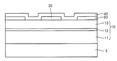
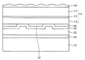
発光構造物10の上には、保護層90が更に配置されてもよい。保護層90は、酸化物又は窒化物で具現されてもよい。保護層90は、例えば、SiO2,SiOx,SiOxNy,Si3N4,Al2O3のような透光性及び絶縁性を有する材質から形成されてもよい。保護層90は、発光構造物10の側面に提供されてもよい。また、保護層90は、発光構造物10の側面だけでなく上部にも提供されてもよい。
それでは、図4乃至図11を参照して、一実施例による発光素子の製造方法を説明する。
例として、第1導電型半導体層11が第1導電型ドーパントとしてn型ドーパントが添加されたn型半導体層として形成され、第2導電型半導体層13が第2導電型ドーパントとしてp型ドーパントが添加されたp型半導体層として形成されてもよい。また、第1導電型半導体層11がp型半導体層として形成され、第2導電型半導体層13がn型半導体層として形成されてもよい。
電流遮断層30は電気絶縁性を有するか、発光構造物10とショットキー接触を形成する材質を利用して形成されてもよい。電流遮断層30は、酸化物、窒化物又は金属で形成されてもよい。電流遮断層30は、例えば、SiO2,SiOx,SiOxNy,Si3N4,Al2O3,TiOx,Ti,Al,Crのうちの少なくとも1つを含んでもよい。アイソレーション層80は、例えば、電気絶縁性を有する材質又は発光構造物10に比べ低い電気伝導性を有する材質で形成されてもよい。アイソレーション層80は、例えば、酸化物又は窒化物で具現されてもよい。例えば、アイソレーション層80は、SiO2,SixOy,Si3N4,SixNy,SiOxNy,Al2O3,TiO2,ITO,AZO,ZnOで形成される群から少なくとも1つが選択されて形成されてもよい。また、アイソレーション層80は、前記電流遮断層30のような物質で形成されてもよく、また互いに異なる物質で形成されてもよい。アイソレーション層80は、チャンネル層として称されてもよい。
反射電極50は、高反射率を有する金属材質で形成されてもよい。例えば、反射電極50は、Ag,Ni,Al,Rh,Pd,Ir,Ru,Mg,Zn,Pt,Cu,Au,Hfのうちの少なくとも1つを含む金属又は合金で形成されてもよい。また、反射電極50は、金属又は合金とITO,IZO,IZTO,IAZO,IGZO,IGTO,ATO,ATOなどの透光性伝導性物質を利用して多層に形成されてもよい。例えば、本実施例における前記反射電極50は、Ag,Al,Ag−Pd−Cu合金又はAg−Cu合金のうち少なくともいずれか一つを含んでもよい。
次に、発光構造物10から基板5を除去する。一つの例として、基板5はレーザリフトオフ(LLO:Laser Lift Off)工程によって除去されてもよい。レーザリフトオフ工程は、基板5の下面にレーザを照射し基板5と発光構造物10を互いに剥離する工程である。
光学シート1051は、表示パネル1051と導光板1041との間に配置され、少なくとも一枚の透光性シートを含む。光学シート1051は、例えば拡散シート、水平及び垂直プリズムシート及び輝度強化シートなどのようなシートのうちの少なくとも1つを含んでもよい。拡散シートは入射される光を拡散させ、水平又は/及び垂直プリズムシートは入射される光を表示領域として集光させ、輝度強化シートは損失される光を再使用して輝度を向上させる。また、表示パネル1061の上には保護シートが配置されてもよく、これに対して限ることはない。
11 第1導電型半導体層
12 活性層
13 第2導電型半導体層
20 電極
30 電流遮断層
40 オーミック接触層
50 反射電極
60 ボンディング層
70 伝導性支持部材
80 アイソレーション層
90 保護層
Claims (22)
- 第1導電型半導体層、前記第1導電型半導体層の下の活性層、前記活性層の下の第2導電型半導体層を有する発光構造物と、
前記第1導電型半導体層に電気的に接続された第1電極と、
前記第2導電型半導体層に電気的に接続された第2電極と
を備え、
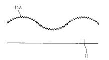
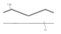
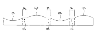
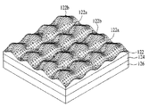
前記第1導電型半導体層の上部表面は連続的な勾配変化を有する曲面を有し、前記第1導電型半導体層の上部表面に凹凸が提供された発光素子。 - 前記発光構造物の表面は、互いに異なる方向の曲率を有する複数個の第1面と第2面が互いに交代に配置されている、請求項1に記載の発光素子。
- 前記第1面及び前記第2面のうちの少なくとも1つの表面には光抽出パターンが形成されている、請求項2に記載の発光素子。
- 前記第1面及び前記第2面は、前記第1導電型半導体層の表面に配置されている、請求項2又は3に記載の発光素子。
- 第1面及び前記第2面のうちの少なくとも1つはマイクロレンズタイプである、請求項2乃至4のいずれかに記載の発光素子。
- 前記第1面及び前記第2面のうちの少なくとも1つは15乃至25マイクロメートルの幅を有する、請求項2乃至5のいずれかに記載の発光素子。
- 前記第1面と前記第2面の幅が同じである、請求項2乃至6のいずれかに記載の発光素子。
- 前記第1面と第2面の表面は互いに対称を成す、請求項2乃至7のいずれかに記載の発光素子。
- 前記第1面は陰刻形状であり、前記第2面は陽刻形状である、請求項2乃至8のいずれかに記載の発光素子。
- 前記第1面と前記第2面の間にフラット(flat)な第3面を更に有する、請求項2乃至9のいずれかに記載の発光素子。
- 前記第1導電型半導体層の上部表面は第1方向の断面上部が連続的な勾配変化を有する曲線を有し、第2方向の断面上部が連続的な勾配変化を有する曲線を有する、請求項1に記載の発光素子。
- 前記第1導電型半導体層の上部表面は第1方向の断面上部が連続的な勾配変化を有する曲線を有し、第2方向の断面上部が互いに異なる勾配を有する直線を有する、請求項1又は11に記載の発光素子。
- 前記第1導電型半導体層の上部表面は、所定形状の反復された曲面を含む請求項1乃至3のいずれかに記載の発光素子。
- 前記第2導電型半導体層の下に配置された電流遮断層を更に備える、請求項1に記載の発光素子。
- 前記第2導電型半導体層と前記第2電極との間、及び前記電流遮断層と前記第2電極との間に配置されたオーミック接触層を更に備える、請求項14に記載の発光素子。
- 前記電流遮断層と前記第1電極は、垂直方向に少なくとも一部領域が重畳された、請求項15に記載の発光素子。
- 前記電流遮断層は、絶縁性を有するか前記発光構造物とショットキー接触する、請求項15又は16に記載の発光素子。
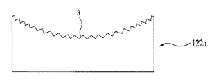
- 前記凹凸は、高さ又は周期が0.8乃至1.2マイクロメートルである、請求項1に記載の発光素子。
- 前記第1電極は、前記第1導電型半導体層に接触された、請求項1に記載の発光素子。
- 前記第2電極は、前記第2導電型半導体層に接触された、請求項1に記載の発光素子。
- 前記第2導電型半導体層の下に配置された反射電極を更に備える、請求項1に記載の発光素子。
- 請求項1乃至21のいずれかに記載の発光素子を備える照明システム。
Applications Claiming Priority (4)
| Application Number | Priority Date | Filing Date | Title |
|---|---|---|---|
| KR10-2011-0048694 | 2011-05-23 | ||
| KR1020110048694A KR20120130617A (ko) | 2011-05-23 | 2011-05-23 | 발광 소자, 발광 소자 패키지, 및 라이트 유닛 |
| KR1020110064597A KR20130007233A (ko) | 2011-06-30 | 2011-06-30 | 발광소자 및 이를 포함하는 조명시스템 |
| KR10-2011-0064597 | 2011-06-30 |
Publications (2)
| Publication Number | Publication Date |
|---|---|
| JP2012244158A true JP2012244158A (ja) | 2012-12-10 |
| JP2012244158A5 JP2012244158A5 (ja) | 2015-03-19 |
Family
ID=45528964
Family Applications (1)
| Application Number | Title | Priority Date | Filing Date |
|---|---|---|---|
| JP2012024435A Pending JP2012244158A (ja) | 2011-05-23 | 2012-02-07 | 発光素子、発光素子パッケージ及びライトユニット |
Country Status (5)
| Country | Link |
|---|---|
| US (1) | US20120299047A1 (ja) |
| EP (1) | EP2528114A3 (ja) |
| JP (1) | JP2012244158A (ja) |
| CN (1) | CN102800772A (ja) |
| TW (1) | TW201248939A (ja) |
Cited By (3)
| Publication number | Priority date | Publication date | Assignee | Title |
|---|---|---|---|---|
| JP2015009384A (ja) * | 2013-06-27 | 2015-01-19 | 日本ゼオン株式会社 | ゴム積層体 |
| JP2015009385A (ja) * | 2013-06-27 | 2015-01-19 | 日本ゼオン株式会社 | ゴム積層体 |
| US9437778B2 (en) | 2013-12-13 | 2016-09-06 | Ushio Denki Kabushiki Kaisha | Semiconductor light-emitting element and method for producing the same |
Families Citing this family (7)
| Publication number | Priority date | Publication date | Assignee | Title |
|---|---|---|---|---|
| CN103117345A (zh) * | 2013-01-31 | 2013-05-22 | 武汉迪源光电科技有限公司 | 一种发光二极管 |
| TWI604632B (zh) | 2013-04-25 | 2017-11-01 | 晶元光電股份有限公司 | 發光二極體裝置 |
| TWI552378B (zh) * | 2014-03-07 | 2016-10-01 | 隆達電子股份有限公司 | 發光二極體晶片 |
| WO2018133940A1 (en) * | 2017-01-19 | 2018-07-26 | Osram Opto Semiconductors Gmbh | Method for producing an optoelectronic element |
| CN106992233A (zh) * | 2017-04-13 | 2017-07-28 | 聚灿光电科技股份有限公司 | 反极性紫外led外延结构及其制备方法 |
| US10720751B2 (en) * | 2017-09-27 | 2020-07-21 | Advanced Semiconductor Engineering, Inc. | Optical package structure, optical module, and method for manufacturing the same |
| CN114628559A (zh) * | 2022-03-21 | 2022-06-14 | 惠州华星光电显示有限公司 | 发光二极管、发光基板以及显示装置 |
Citations (8)
| Publication number | Priority date | Publication date | Assignee | Title |
|---|---|---|---|---|
| JP2004186268A (ja) * | 2002-11-29 | 2004-07-02 | Shin Etsu Handotai Co Ltd | 発光素子 |
| JP2005317663A (ja) * | 2004-04-27 | 2005-11-10 | Shin Etsu Handotai Co Ltd | 発光素子の製造方法及び発光素子 |
| JP2007036240A (ja) * | 2005-07-22 | 2007-02-08 | Samsung Electro Mech Co Ltd | 垂直構造の窒化ガリウム系発光ダイオード素子、及びその製造方法 |
| JP2007335874A (ja) * | 2006-06-16 | 2007-12-27 | High Power Optoelectronics Inc | 半導体発光素子および同素子の製造方法 |
| JP2010050157A (ja) * | 2008-08-19 | 2010-03-04 | Shin Etsu Handotai Co Ltd | 発光素子及びその製造方法 |
| JP2010147056A (ja) * | 2008-12-16 | 2010-07-01 | Stanley Electric Co Ltd | Ii−vi族またはiii−v族化合物系半導体発光素子用エピタキシャルウエハ、および、その製造方法 |
| JP2011086909A (ja) * | 2009-10-15 | 2011-04-28 | Lg Innotek Co Ltd | 半導体発光素子 |
| JP2012129234A (ja) * | 2010-12-13 | 2012-07-05 | Toshiba Corp | 半導体発光素子 |
Family Cites Families (9)
| Publication number | Priority date | Publication date | Assignee | Title |
|---|---|---|---|---|
| US5814839A (en) * | 1995-02-16 | 1998-09-29 | Sharp Kabushiki Kaisha | Semiconductor light-emitting device having a current adjusting layer and a uneven shape light emitting region, and method for producing same |
| JP3802424B2 (ja) * | 2002-01-15 | 2006-07-26 | 株式会社東芝 | 半導体発光素子及びその製造方法 |
| US7335920B2 (en) * | 2005-01-24 | 2008-02-26 | Cree, Inc. | LED with current confinement structure and surface roughening |
| US20060204865A1 (en) * | 2005-03-08 | 2006-09-14 | Luminus Devices, Inc. | Patterned light-emitting devices |
| DE102005033005A1 (de) * | 2005-07-14 | 2007-01-18 | Osram Opto Semiconductors Gmbh | Optoelektronischer Chip |
| KR101289230B1 (ko) * | 2007-07-23 | 2013-07-29 | 엘지이노텍 주식회사 | 발광 소자 및 그 제조방법 |
| US8461613B2 (en) * | 2008-05-27 | 2013-06-11 | Interlight Optotech Corporation | Light emitting device |
| US8008683B2 (en) * | 2008-10-22 | 2011-08-30 | Samsung Led Co., Ltd. | Semiconductor light emitting device |
| KR101028277B1 (ko) * | 2010-05-25 | 2011-04-11 | 엘지이노텍 주식회사 | 발광 소자, 발광 소자 제조방법, 발광 소자 패키지 및 라이트 유닛 |
-
2012
- 2012-01-19 EP EP20120151758 patent/EP2528114A3/en not_active Withdrawn
- 2012-01-31 US US13/362,340 patent/US20120299047A1/en not_active Abandoned
- 2012-02-03 TW TW101103531A patent/TW201248939A/zh unknown
- 2012-02-07 JP JP2012024435A patent/JP2012244158A/ja active Pending
- 2012-03-23 CN CN2012100855621A patent/CN102800772A/zh active Pending
Patent Citations (8)
| Publication number | Priority date | Publication date | Assignee | Title |
|---|---|---|---|---|
| JP2004186268A (ja) * | 2002-11-29 | 2004-07-02 | Shin Etsu Handotai Co Ltd | 発光素子 |
| JP2005317663A (ja) * | 2004-04-27 | 2005-11-10 | Shin Etsu Handotai Co Ltd | 発光素子の製造方法及び発光素子 |
| JP2007036240A (ja) * | 2005-07-22 | 2007-02-08 | Samsung Electro Mech Co Ltd | 垂直構造の窒化ガリウム系発光ダイオード素子、及びその製造方法 |
| JP2007335874A (ja) * | 2006-06-16 | 2007-12-27 | High Power Optoelectronics Inc | 半導体発光素子および同素子の製造方法 |
| JP2010050157A (ja) * | 2008-08-19 | 2010-03-04 | Shin Etsu Handotai Co Ltd | 発光素子及びその製造方法 |
| JP2010147056A (ja) * | 2008-12-16 | 2010-07-01 | Stanley Electric Co Ltd | Ii−vi族またはiii−v族化合物系半導体発光素子用エピタキシャルウエハ、および、その製造方法 |
| JP2011086909A (ja) * | 2009-10-15 | 2011-04-28 | Lg Innotek Co Ltd | 半導体発光素子 |
| JP2012129234A (ja) * | 2010-12-13 | 2012-07-05 | Toshiba Corp | 半導体発光素子 |
Cited By (3)
| Publication number | Priority date | Publication date | Assignee | Title |
|---|---|---|---|---|
| JP2015009384A (ja) * | 2013-06-27 | 2015-01-19 | 日本ゼオン株式会社 | ゴム積層体 |
| JP2015009385A (ja) * | 2013-06-27 | 2015-01-19 | 日本ゼオン株式会社 | ゴム積層体 |
| US9437778B2 (en) | 2013-12-13 | 2016-09-06 | Ushio Denki Kabushiki Kaisha | Semiconductor light-emitting element and method for producing the same |
Also Published As
| Publication number | Publication date |
|---|---|
| TW201248939A (en) | 2012-12-01 |
| EP2528114A2 (en) | 2012-11-28 |
| US20120299047A1 (en) | 2012-11-29 |
| CN102800772A (zh) | 2012-11-28 |
| EP2528114A3 (en) | 2014-07-09 |
Similar Documents
| Publication | Publication Date | Title |
|---|---|---|
| US9899567B2 (en) | Light emitting device | |
| US8575635B2 (en) | Light emitting device, light emitting device package, and lighting system | |
| JP5788210B2 (ja) | 発光素子、発光素子パッケージ | |
| KR102197082B1 (ko) | 발광 소자 및 이를 포함하는 발광소자 패키지 | |
| JP2012244158A (ja) | 発光素子、発光素子パッケージ及びライトユニット | |
| US8431944B2 (en) | Light emitting device, light emitting device package, and lighting system | |
| KR20110101712A (ko) | 발광 소자, 발광 소자 제조방법 및 발광 소자 패키지 | |
| JP2013046049A (ja) | 発光素子及び発光素子パッケージ | |
| KR101786094B1 (ko) | 발광 소자, 발광 소자 패키지, 및 라이트 유닛 | |
| KR101795038B1 (ko) | 발광 소자 및 발광 소자 패키지 | |
| US9559254B2 (en) | Light emitting device and light emitting device package | |
| KR101880445B1 (ko) | 발광소자, 발광소자 제조방법, 발광소자 패키지, 및 라이트 유닛 | |
| KR101865919B1 (ko) | 발광 소자, 발광 소자 패키지, 라이트 유닛, 발광 소자 제조방법 | |
| KR101795037B1 (ko) | 발광 소자 및 발광 소자 패키지 | |
| KR101818753B1 (ko) | 발광소자 | |
| KR101805121B1 (ko) | 발광 소자, 발광 소자 패키지 및 조명 시스템 | |
| KR20120130617A (ko) | 발광 소자, 발광 소자 패키지, 및 라이트 유닛 | |
| KR101759901B1 (ko) | 발광 소자, 발광 소자 패키지 및 조명 시스템 | |
| KR101683906B1 (ko) | 발광 소자, 발광 소자 제조방법, 발광 소자 패키지 및 조명 시스템 | |
| KR20130016667A (ko) | 발광소자, 발광소자 패키지, 및 라이트 유닛 | |
| KR20130007171A (ko) | 발광 소자, 발광 소자 패키지, 및 라이트 유닛 | |
| KR20130007172A (ko) | 발광 소자, 발광 소자 패키지, 및 라이트 유닛 | |
| KR20120068295A (ko) | 발광 소자 | |
| KR20130069207A (ko) | 발광소자, 발광소자 패키지 및 라이트 유닛 | |
| KR20130007233A (ko) | 발광소자 및 이를 포함하는 조명시스템 |
Legal Events
| Date | Code | Title | Description |
|---|---|---|---|
| RD04 | Notification of resignation of power of attorney |
Free format text: JAPANESE INTERMEDIATE CODE: A7424 Effective date: 20121005 |
|
| A521 | Request for written amendment filed |
Free format text: JAPANESE INTERMEDIATE CODE: A523 Effective date: 20150203 |
|
| A621 | Written request for application examination |
Free format text: JAPANESE INTERMEDIATE CODE: A621 Effective date: 20150203 |
|
| A977 | Report on retrieval |
Free format text: JAPANESE INTERMEDIATE CODE: A971007 Effective date: 20151126 |
|
| A131 | Notification of reasons for refusal |
Free format text: JAPANESE INTERMEDIATE CODE: A131 Effective date: 20151208 |
|
| A02 | Decision of refusal |
Free format text: JAPANESE INTERMEDIATE CODE: A02 Effective date: 20160510 |