JP2012243401A - Transparent conductive film and organic electroluminescent element - Google Patents
Transparent conductive film and organic electroluminescent element Download PDFInfo
- Publication number
- JP2012243401A JP2012243401A JP2011109131A JP2011109131A JP2012243401A JP 2012243401 A JP2012243401 A JP 2012243401A JP 2011109131 A JP2011109131 A JP 2011109131A JP 2011109131 A JP2011109131 A JP 2011109131A JP 2012243401 A JP2012243401 A JP 2012243401A
- Authority
- JP
- Japan
- Prior art keywords
- film
- organic
- resin
- mmol
- acid
- Prior art date
- Legal status (The legal status is an assumption and is not a legal conclusion. Google has not performed a legal analysis and makes no representation as to the accuracy of the status listed.)
- Withdrawn
Links
Images

Abstract
Description
本発明は液晶表示素子、有機発光素子、無機電界発光素子、太陽電池、電磁波シールド、電子ペーパー、タッチパネル等の各種分野において好適に用いることができる透明電極、更に該透明電極を用いた有機エレクトロルミネッセンス素子(以後、有機EL素子ともいう)に関する。 The present invention is a transparent electrode that can be suitably used in various fields such as a liquid crystal display element, an organic light emitting element, an inorganic electroluminescent element, a solar cell, an electromagnetic wave shield, electronic paper, and a touch panel, and further an organic electroluminescence using the transparent electrode. The present invention relates to an element (hereinafter also referred to as an organic EL element).
近年、薄型TV需要の高まりに伴い、液晶・プラズマ・有機エレクトロルミネッセンス・フィールドエミッション等、各種方式のディスプレイ技術が開発されている。これら表示方式の異なる何れのディスプレイにおいても、透明電極は必須の構成技術となっている。又、テレビ以外でも、タッチパネルや携帯電話、電子ペーパー、各種太陽電池、各種エレクトロルミネッセンス調光素子においても、透明電極は欠くことのできない技術要素となっている。 In recent years, various types of display technologies such as liquid crystal, plasma, organic electroluminescence, and field emission have been developed in response to the increasing demand for thin TVs. In any of these displays with different display methods, the transparent electrode is an essential constituent technology. In addition to televisions, transparent electrodes are an indispensable technical element in touch panels, mobile phones, electronic paper, various solar cells, and various electroluminescence light control elements.
従来透明電極は、ガラスや透明なプラスチックフィルム等の透明基材上に、インジウム−スズの複合酸化物(ITO)膜を真空蒸着法やスパッタリング法で製膜したITO透明電極が主に使用されてきた。しかし、ITOに用いられているインジウムはレアメタルであり、かつ価格の高騰により、脱インジウムが望まれている。又、ディスプレイの大画面化、生産性向上に伴い、フレキシブル基板を用いたロールツウロールの生産技術が所望されている。 Conventionally, an ITO transparent electrode in which a composite oxide (ITO) film of indium-tin is formed on a transparent substrate such as glass or a transparent plastic film by a vacuum deposition method or a sputtering method has been mainly used. It was. However, indium used in ITO is a rare metal and removal of indium is desired due to the rising price. In addition, with the increase in display screen and productivity, a roll-to-roll production technique using a flexible substrate is desired.
近年、このような大面積かつ低抵抗値が要求される製品にも対応できるよう、パターン状に形成された金属細線に導電性ポリマー等の透明導電膜を積層し、電流の面均一性と高い導電性を併せ持つ透明導電フィルムが開発されている(例えば、特許文献1参照)。しかしながら、このような構成では、有機電子デバイスのリークの原因となる金属細線の凹凸を、導電性ポリマー等の透明導電膜でなだらかにする必要があり、導電性ポリマーの厚膜化が必須となる。しかし、導電性ポリマーは可視光領域に吸収を有するため、厚膜化すると、透明電極の透明性が著しく低下してしまうという課題を有していた。 In recent years, a transparent conductive film such as a conductive polymer is laminated on a thin metal wire formed in a pattern so that it can be used for products requiring such a large area and a low resistance value, and the surface uniformity of current is high. A transparent conductive film having both conductivity has been developed (see, for example, Patent Document 1). However, in such a configuration, it is necessary to smooth the irregularities of the fine metal wires that cause leakage of the organic electronic device with a transparent conductive film such as a conductive polymer, and it is essential to increase the thickness of the conductive polymer. . However, since the conductive polymer has absorption in the visible light region, there is a problem that when the film is thickened, the transparency of the transparent electrode is significantly lowered.
又、導電性と透明性を両立するとして、細線構造部上へ導電性ポリマーと絶縁性ポリマーの混合物を積層する技術が開示されている(例えば、特許文献2)。しかし、絶縁性ポリマーの添加は導電率の低下や導電性ポリマーへの相溶性の観点からヘイズ等の光学性能の劣化を引き起こすという課題を有していた。 Moreover, the technique which laminates | stacks the mixture of a conductive polymer and an insulating polymer on a thin wire | line structure part is disclosed as making electroconductivity and transparency compatible (for example, patent document 2). However, the addition of an insulating polymer has a problem that it causes deterioration of optical performance such as haze from the viewpoint of a decrease in conductivity and compatibility with the conductive polymer.
更に、導電性ポリマーと相溶する高分子として、ポリビニルピロリドン(PVP)、ポリ(ビニルピリジン)とポリ(酢酸ビニル)とのコポリマー(PVPy−VAc)、ポリメタクリル酸(PMAA)、ポリ(ヒドロキシエチルアクリレート)とポリ(メタクリル酸)とのコポリマー(PHEA−MAA)、ポリ(2−ヒドロキシエチルメタクリレート)、ポリビニルブチラール(PVB)とからなる群から選択されたポリマー又はコポリマーが開示されている(例えば、特許文献3、4)。しかし、これらのポリマーを用いた場合、膜強度不足のため、蒸着やスピンコートによる積層を行った場合膜表面が乱れ、有機電子デバイスを作製するとリークが発生するという課題を有していた。
Furthermore, as a polymer compatible with the conductive polymer, polyvinylpyrrolidone (PVP), a copolymer of poly (vinyl pyridine) and poly (vinyl acetate) (PVPy-VAc), polymethacrylic acid (PMAA), poly (hydroxyethyl) A polymer or copolymer selected from the group consisting of (acrylate) and poly (methacrylic acid) copolymer (PHEA-MAA), poly (2-hydroxyethyl methacrylate), polyvinyl butyral (PVB) is disclosed (eg,
更に、導電性ポリマー等の透明導電膜を用いる場合、その透明導電膜中に水分が残留していると、有機電子デバイスの性能を劣化させることが知られており、透明導電膜中の水分除去が必須となる。しかし、近年、透明基板についてフレキシブル性やコスト面から透明フィルムが用いられることが多くなってきており、導電性ポリマー等の透明導電膜を、フィルムが変形しないガラス転移温度Tg以下の低温で加熱する場合、透明導電膜中に水分が残留してしまい、透明導電膜の乾燥が課題であった。 Furthermore, when a transparent conductive film such as a conductive polymer is used, it is known that if water remains in the transparent conductive film, the performance of the organic electronic device is deteriorated. Is essential. However, in recent years, a transparent film has been increasingly used from the viewpoint of flexibility and cost for a transparent substrate, and a transparent conductive film such as a conductive polymer is heated at a low temperature below the glass transition temperature Tg at which the film does not deform. In this case, moisture remains in the transparent conductive film, and drying of the transparent conductive film has been a problem.
本発明は上記課題に鑑みなされたものであり、本発明の目的は、透明性、導電性、膜強度に優れると共に、高温、高湿度環境下においても透明性、導電性、膜強度の劣化が少なく、安定性、発光均一性に優れ、かつ発光均一性の劣化が少なく発光寿命に優れる有機EL素子を与える透明電極を提供することにある。 The present invention has been made in view of the above-mentioned problems, and the object of the present invention is excellent in transparency, conductivity, and film strength, as well as deterioration in transparency, conductivity, and film strength even in a high temperature and high humidity environment. An object of the present invention is to provide a transparent electrode that provides an organic EL device that is less in stability, excellent in light emission uniformity, and less in light emission uniformity and excellent in light emission life.
更に、当該電極を用いた、発光均一性が高く、発光均一性の劣化が少なく寿命に優れる有機EL素子を提供することにある。 It is another object of the present invention to provide an organic EL device that uses the electrode and has high light emission uniformity, little deterioration of light emission uniformity, and excellent life.
これまで透明導電膜用塗布液としては、導電性と透過率を両立させるために3,4−ポリエチレンジオキシチオフェンポリスルホネート(PEDOT/PSS)等の水分散性導電性ポリマーと水溶性バインダーを含有する組成物が開発されてきた。ここにおいて、水溶性ポリマーとしては水分散性導電性ポリマーとの相溶性の観点から、親水性のバインダーが検討されてきた。しかし、透明基板としてフレキシブル性への要求が高まり、ポリエチレンテレフタレート等の樹脂フィルムを使用すると、樹脂フィルムにおいて変形を避けるとの観点から、乾燥温度はガラス基板よりも低温となる。その結果、親水性バインダーの影響で膜中からの水分除去が困難になり、これら透明導電膜を用いた素子の性能を著しく劣化させていた。これらの現象を改良すべく鋭意検討した結果、透明導電膜中に、水分散性導電性ポリマーと共に、バインダー樹脂として、バインダーの繰り返し単位中にカルボキシ基を有する構造単位とカルボキシ基を含有しない構造単位を含む樹脂を用いる本発明の構成に至った。 Conventionally, the coating liquid for transparent conductive film contains water-dispersible conductive polymer such as 3,4-polyethylenedioxythiophene polysulfonate (PEDOT / PSS) and water-soluble binder in order to achieve both conductivity and transmittance. Compositions have been developed. Here, hydrophilic binders have been studied as water-soluble polymers from the viewpoint of compatibility with water-dispersible conductive polymers. However, the demand for flexibility increases as a transparent substrate, and when a resin film such as polyethylene terephthalate is used, the drying temperature is lower than that of the glass substrate from the viewpoint of avoiding deformation in the resin film. As a result, it was difficult to remove moisture from the film due to the influence of the hydrophilic binder, and the performance of the device using these transparent conductive films was significantly deteriorated. As a result of intensive studies to improve these phenomena, a structural unit having a carboxy group in a repeating unit of a binder and a structural unit not containing a carboxy group as a binder resin together with a water-dispersible conductive polymer in a transparent conductive film It came to the structure of this invention using the resin containing this.
即ち、本発明は、本発明構成の如く、第2導電層に、部分エステル化ポリカルボン酸樹脂を用いており、これは、繰り返し単位中にカルボキシ基を有する構造単位とカルボキシ基を含有しない構造単位を適切にコントロールしたバインダー樹脂であって、本発明の課題は、バインダー樹脂として、これらの部分エステル化ポリカルボン酸樹脂を含有させることにより達成できることが判明し本発明に至った。 That is, the present invention uses a partially esterified polycarboxylic acid resin for the second conductive layer as in the structure of the present invention, which has a structure unit having a carboxy group in a repeating unit and a structure not containing a carboxy group. It was a binder resin in which the units were appropriately controlled, and it was found that the object of the present invention can be achieved by including these partially esterified polycarboxylic acid resins as the binder resin.
部分的にエステル化されたポリカルボン酸を得る手法としては、メタクリル酸メチルなどの完全にエステル化したモノマー原料をもとにポリメタクリル酸メチルのような完全にエステル化されたポリマーを得た後、アルカリにより部分的にケン化する方法、アクリル酸などのカルボキシ基を有したモノマー類とアクリル酸メチルなどのエステル化されたモノマーを共重合する方法、グリシジル化合物をポリカルボン酸に作用させて部分的にエステル化する方法などが知られている。ここで、完全にエステル化されたポリマーをケン化によって部分的にエステル化する方法では、重合反応でポリマーを得た後に再度アルカリなどによりケン化処理をするために、ポリマーから不純物を除くのが困難になること、共重合する場合、モノマーの反応性により完全にランダムな分布の部分エステル化ポリマーを得るのが困難であること、グリシジル化合物を使用すると、定量的に導入するのが困難であるという問題があった。 A technique for obtaining a partially esterified polycarboxylic acid is to obtain a fully esterified polymer such as polymethyl methacrylate from a fully esterified monomer raw material such as methyl methacrylate. , A method of partially saponifying with an alkali, a method of copolymerizing monomers having a carboxy group such as acrylic acid and an esterified monomer such as methyl acrylate, and the like by allowing a glycidyl compound to act on a polycarboxylic acid. For example, a method of esterifying is known. Here, in the method of partially esterifying a completely esterified polymer by saponification, impurities are removed from the polymer in order to saponify again with alkali after obtaining the polymer by polymerization reaction. When it is difficult to copolymerize, it is difficult to obtain a partially esterified polymer with a completely random distribution due to the reactivity of the monomers, and when using a glycidyl compound, it is difficult to introduce quantitatively. There was a problem.
本発明は第2導電層に導電性ポリマーとカルボキシ基の数とカルボキシ基のランダムな分布とをコントロールしたバインダー樹脂を用いることで透明導電膜の透明性と導電性を両立し、かつ膜強度に優れ、更に高温、高湿度環境下における環境試験後でも高い導電性と透明性及び良好な膜強度を併せ持つ、安定性の優れた透明電極、及び該透明電極を用いた高寿命の有機エレクトロルミネッセンス素子が、得られることを見出したものである。 In the present invention, the second conductive layer is made of a conductive polymer, a binder resin in which the number of carboxy groups and the random distribution of carboxy groups are controlled, so that the transparency and conductivity of the transparent conductive film are compatible and the film strength is increased. Excellent transparent electrode having excellent conductivity, transparency and good film strength even after environmental test under high temperature and high humidity environment, and long-life organic electroluminescence device using the transparent electrode Has been found to be obtained.
本発明の目的は、下記の構成を採ることにより達成される。 The object of the present invention is achieved by adopting the following configuration.
1.基材上にパターン状に形成された金属材料からなる第1導電層と、導電性ポリマー及び部分エステル化ポリカルボン酸樹脂を含有する第2導電層を有する透明導電膜において、前記、部分エステル化ポリカルボン酸樹脂はポリカルボン酸にアセタール化合物を反応させた樹脂であることを特徴とする透明導電膜。 1. In the transparent conductive film having a first conductive layer made of a metal material formed in a pattern on a substrate and a second conductive layer containing a conductive polymer and a partially esterified polycarboxylic acid resin, the partial esterification A transparent conductive film, wherein the polycarboxylic acid resin is a resin obtained by reacting a polycarboxylic acid with an acetal compound.
2.前記部分エステル化ポリカルボン酸樹脂のカルボキシ基濃度が0.5mmol/gから5.0mmol/gであることを特徴とする前記1に記載の透明導電膜。 2. 2. The transparent conductive film according to 1 above, wherein the partially esterified polycarboxylic acid resin has a carboxy group concentration of 0.5 mmol / g to 5.0 mmol / g.
3.前記部分エステル化ポリカルボン酸樹脂のポリカルボン酸が、ポリアクリル酸、ポリメタアクリル酸、ポリカルボキシスチレン及びこれらの共重合体の中から選ばれたものであることを特徴とする前記1または2に記載の透明導電膜。 3. 1 or 2 above, wherein the polycarboxylic acid of the partially esterified polycarboxylic acid resin is selected from polyacrylic acid, polymethacrylic acid, polycarboxystyrene, and copolymers thereof. The transparent conductive film as described in 2.
4.前記1〜3のいずれか1項に記載の透明導電膜を用いたことを特徴とする有機エレクトロルミネッセンス素子。 4). The organic electroluminescent element characterized by using the transparent conductive film of any one of said 1-3.
本発明の上記手段により、透明性、導電性、膜強度に優れると共に、高温、高湿度環境下においても透明性、導電性、膜強度の劣化が少なく、安定性、発光均一性に優れ、かつ発光均一性の劣化が少なく発光寿命に優れる有機EL素子を与える透明電極を提供できる。 By the above means of the present invention, the transparency, conductivity and film strength are excellent, and transparency, conductivity and film strength are hardly deteriorated even in a high temperature and high humidity environment, and stability and light emission uniformity are excellent. It is possible to provide a transparent electrode that provides an organic EL device that has little emission uniformity deterioration and excellent emission lifetime.
更に、当該電極を用いた発光均一性が高く、発光均一性の劣化が少なく寿命に優れる有機EL素子を提供できる。 Furthermore, it is possible to provide an organic EL element that has high emission uniformity using the electrode, has little deterioration in emission uniformity, and has an excellent lifetime.
以下、本発明を実施するための形態について説明する。 Hereinafter, modes for carrying out the present invention will be described.
本発明の構成の透明導電膜の一例を図解した概略図を示すと図1の如くである。 FIG. 1 is a schematic diagram illustrating an example of the transparent conductive film having the structure of the present invention.
図1において、1はパターン状に形成された金属材料からなる第1導電層、2は導電性ポリマーを含有する第2導電層、3は基材を示す。本発明の構成における特徴は、第2導電層2に部分的にエステル化されたポリカルボン酸樹脂を含有する。
In FIG. 1, 1 is a first conductive layer made of a metal material formed in a pattern, 2 is a second conductive layer containing a conductive polymer, and 3 is a substrate. The feature of the configuration of the present invention includes a polycarboxylic acid resin partially esterified on the second
《第2導電層》
〈部分的にエステル化されたポリカルボン酸樹脂〉
本発明において、第2導電層に水分散性導電性ポリマーと共にバインダー樹脂として用いる部分的にエステル化されたポリカルボン酸について説明する。
<< Second conductive layer >>
<Partially esterified polycarboxylic acid resin>
In the present invention, a partially esterified polycarboxylic acid used as a binder resin together with a water-dispersible conductive polymer in the second conductive layer will be described.
本発明におけるポリカルボン酸とは、ポリマー主鎖又は側鎖にカルボキシ基を有するものである。このようなものとしては、テトラカルボン酸又はその酸二無水物とジアミンを反応させて得ることができるポリアミド酸、あるいはアクリル酸やメタアクリル酸、マレイン酸、カルボキシスチレンを重合させて得られるポリアクリル酸、ポリメタアクリル酸、ポリマレイン酸、ポリカルボキシスチレンやこれらと他のモノマー類であるアクリル酸メチル、メタクリル酸メチル、スチレン、エチレン、プロピレン、その他のビニル化合物などを共重合させたものを挙げることができる。 The polycarboxylic acid in the present invention has a carboxy group in the polymer main chain or side chain. Such as polyacrylic acid obtained by reacting tetracarboxylic acid or its acid dianhydride and diamine, or polyacrylic acid obtained by polymerizing acrylic acid, methacrylic acid, maleic acid or carboxystyrene. List the acid, polymethacrylic acid, polymaleic acid, polycarboxystyrene, and these and other monomers such as methyl acrylate, methyl methacrylate, styrene, ethylene, propylene, and other vinyl compounds. Can do.
又、これ以外のカルボキシ基を有するポリマーも同様に使用することができる。 Moreover, the polymer which has a carboxy group other than this can be used similarly.
部分エステル化ポリカルボン酸樹脂はこれらのポリカルボン酸にアセタール化合物を反応させエステル化することで得られる。 The partially esterified polycarboxylic acid resin can be obtained by reacting these polycarboxylic acids with an acetal compound and esterifying them.
本発明における部分エステル化ポリカルボン酸のエステル化度は、残存しているカルボキシ基の量を定量することで求めることが出来る。この残存しているカルボキシ基は滴定法により求めることが最も簡便かつ正確である。このカルボキシ基濃度としては、0.5mmol/gから5.0mmol/gであることが好ましい。これより、エステル化が進行して、0.5mmol/gよりカルボキシ基濃度が低くなると、あらかじめエステル化したモノマーから得た完全エステル化ポリマーと溶解性で違いが無くなる。又、残存しているカルボキシ基が5.0mmol/gより多くなると、水に溶解しすぎるなどの問題が現れるため好ましくない。 The degree of esterification of the partially esterified polycarboxylic acid in the present invention can be determined by quantifying the amount of the remaining carboxy group. The remaining carboxy group is most easily and accurately determined by a titration method. The carboxy group concentration is preferably 0.5 mmol / g to 5.0 mmol / g. Accordingly, when esterification proceeds and the carboxy group concentration becomes lower than 0.5 mmol / g, there is no difference in solubility from the completely esterified polymer obtained from the esterified monomer in advance. Further, if the remaining carboxy group exceeds 5.0 mmol / g, problems such as excessive dissolution in water appear, which is not preferable.
本発明において、エステル化度の調整は、エステル化剤であるアセタール化合物の添加量により制御することが好ましい。アセタール化合物の添加量に応じてエステル化率を自由に制御することができる。又、その他のエステル化試薬を使用することもできる。本発明においてアセタール化合物とは、カルボニル基にアルコールを2当量反応させた化合物のことで、いわゆるアセタール類、ケタール類等を総称して言う。具体的には、N,N−ジメチルホルムアミド、N−メチル−ピロリドン、ガンマブチロラクトン、N,N−ジメチルアセトアミド、N,N−ジエチルホルムアミド、炭酸エチレン、炭酸プロピレンなどのカルボニル基を有する双極性非プロトン溶媒のアセタール化合物が好ましい。このようなアセタール化合物を、反応させようとするポリカルボン酸溶液に混合し、0℃から100℃で10分から8時間反応させることで部分エステル化ポリカルボン酸を得ることが出来る。これらのアセタール化合物は、H.Meerwein、Angewante Chemie 71巻、530頁(1959年)に合成法が記載されている。 In the present invention, the adjustment of the degree of esterification is preferably controlled by the amount of an acetal compound that is an esterifying agent. The esterification rate can be freely controlled according to the amount of the acetal compound added. Other esterification reagents can also be used. In the present invention, an acetal compound is a compound obtained by reacting two equivalents of an alcohol with a carbonyl group, and collectively refers to so-called acetals and ketals. Specifically, bipolar aprotic having a carbonyl group such as N, N-dimethylformamide, N-methyl-pyrrolidone, gamma butyrolactone, N, N-dimethylacetamide, N, N-diethylformamide, ethylene carbonate, propylene carbonate The solvent acetal compound is preferred. A partially esterified polycarboxylic acid can be obtained by mixing such an acetal compound with a polycarboxylic acid solution to be reacted and reacting at 0 ° C. to 100 ° C. for 10 minutes to 8 hours. These acetal compounds are described in H.C. A synthetic method is described in Meerwein, Angewante Chemie 71, 530 (1959).
本発明における、アセタール化合物としては、上記双極性非プロトン溶媒のジメチルアセタール、ジエチルアセタール、ジプロピルアセタール、ジブチルアセタール、ジヘキシルアセタール、ジオクチルアセタール、ジデシルアセタールなどの炭素数1から10までのジアルキルアセタール、ジビニルアセタール、ジアリルアセタール、ジ(エチルメタクリレート)アセタール、ジ(エチルアクリレート)アセタールなどの不飽和結合を有したアセタール化合物などを好ましく使用することもできる。特に不飽和結合を有したアセタール化合物を使用すると、紫外線などの化学線で架橋反応を起こすために、化学線硬化型の部分エステルポリカルボン酸を得ることができる。 In the present invention, the acetal compound is a dialkyl acetal having 1 to 10 carbon atoms such as dimethyl acetal, diethyl acetal, dipropyl acetal, dibutyl acetal, dihexyl acetal, dioctyl acetal, didecyl acetal, etc. Acetal compounds having an unsaturated bond such as divinyl acetal, diallyl acetal, di (ethyl methacrylate) acetal, di (ethyl acrylate) acetal, and the like can also be preferably used. In particular, when an acetal compound having an unsaturated bond is used, a cross-linking reaction is caused by actinic radiation such as ultraviolet rays, so that actinic radiation curable partial ester polycarboxylic acid can be obtained.
本発明の部分的にエステル化されたポリカルボン酸樹脂の分子量は3,000〜2,000,000の範囲が好ましく、より好ましくは4,000〜500,000、更に好ましくは5000〜100000の範囲内である。 The molecular weight of the partially esterified polycarboxylic acid resin of the present invention is preferably in the range of 3,000 to 2,000,000, more preferably 4,000 to 500,000, still more preferably 5,000 to 100,000. Is within.
本発明の部分的にエステル化されたポリカルボン酸樹脂の数平均分子量、分子量分布の測定は、一般的に知られているゲルパーミエーションクロマトグラフィー(GPC)により行うことができる。使用する溶媒は、バインダー樹脂が溶解すれば特に限りはなく、THF(テトラヒドロフラン)、DMF(ジメチルホルムアミド)、CH2Cl2が好ましく、より好ましくはTHF、DMFであり、更に好ましくはDMFである。又、測定温度も特に制限はないが40℃が好ましい。 The number average molecular weight and molecular weight distribution of the partially esterified polycarboxylic acid resin of the present invention can be measured by generally known gel permeation chromatography (GPC). The solvent to be used is not particularly limited as long as the binder resin dissolves, and THF (tetrahydrofuran), DMF (dimethylformamide), and CH 2 Cl 2 are preferable, more preferably THF and DMF, and still more preferably DMF. The measurement temperature is not particularly limited, but 40 ° C. is preferable.
〈導電性ポリマー〉
本発明では、第2導電層は導電性ポリマーを含有する。
<Conductive polymer>
In the present invention, the second conductive layer contains a conductive polymer.
本発明に係る導電性ポリマーは、π共役系導電性高分子とポリ陰イオンとを有してなる導電性ポリマーである。こうした導電性ポリマーは、後述するπ共役系導電性高分子を形成する前駆体モノマーを、適切な酸化剤と酸化触媒と後述のポリ陰イオンの存在下で化学酸化重合することによって容易に製造できる。 The conductive polymer according to the present invention is a conductive polymer having a π-conjugated conductive polymer and a polyanion. Such a conductive polymer can be easily produced by chemical oxidative polymerization of a precursor monomer that forms a π-conjugated conductive polymer described later in the presence of an appropriate oxidizing agent, an oxidation catalyst, and a poly anion described later. .
(π共役系導電性高分子)
本発明に用いるπ共役系導電性高分子としては、特に限定されず、ポリチオフェン(基本のポリチオフェンを含む、以下同様)類、ポリピロール類、ポリインドール類、ポリカルバゾール類、ポリアニリン類、ポリアセチレン類、ポリフラン類、ポリパラフェニレンビニレン類、ポリアズレン類、ポリパラフェニレン類、ポリパラフェニレンサルファイド類、ポリイソチアナフテン類、ポリチアジル類、の鎖状導電性ポリマーを利用することができる。中でも、導電性、透明性、安定性等の観点からポリチオフェン類やポリアニリン類が好ましい。ポリエチレンジオキシチオフェンが最も好ましい。
(Π-conjugated conductive polymer)
The π-conjugated conductive polymer used in the present invention is not particularly limited, and includes polythiophenes (including basic polythiophenes, the same applies hereinafter), polypyrroles, polyindoles, polycarbazoles, polyanilines, polyacetylenes, polyfurans. , Polyparaphenylene vinylenes, polyazulenes, polyparaphenylenes, polyparaphenylene sulfides, polyisothianaphthenes, polythiazyl chain conductive polymers can be used. Of these, polythiophenes and polyanilines are preferable from the viewpoints of conductivity, transparency, stability, and the like. Most preferred is polyethylene dioxythiophene.
(π共役系導電性高分子前駆体モノマー)
π共役系導電性高分子の形成に用いられる前駆体モノマーは、分子内にπ共役系を有し、適切な酸化剤の作用によって高分子化した際にもその主鎖にπ共役系が形成されるものである。例えば、ピロール類及びその誘導体、チオフェン類及びその誘導体、アニリン類及びその誘導体等が挙げられる。
(Π-conjugated conductive polymer precursor monomer)
Precursor monomers used in the formation of π-conjugated conductive polymers have a π-conjugated system in the molecule, and even when polymerized by the action of an appropriate oxidant, a π-conjugated system is formed in the main chain. It is what is done. Examples thereof include pyrroles and derivatives thereof, thiophenes and derivatives thereof, anilines and derivatives thereof, and the like.
前駆体モノマーの具体例としては、ピロール、3−メチルピロール、3−エチルピロール、3−n−プロピルピロール、3−ブチルピロール、3−オクチルピロール、3−デシルピロール、3−ドデシルピロール、3,4−ジメチルピロール、3,4−ジブチルピロール、3−カルボキシピロール、3−メチル−4−カルボキシピロール、3−メチル−4−カルボキシエチルピロール、3−メチル−4−カルボキシブチルピロール、3−ヒドロキシピロール、3−メトキシピロール、3−エトキシピロール、3−ブトキシピロール、3−ヘキシルオキシピロール、3−メチル−4−ヘキシルオキシピロール、チオフェン、3−メチルチオフェン、3−エチルチオフェン、3−プロピルチオフェン、3−ブチルチオフェン、3−ヘキシルチオフェン、3−ヘプチルチオフェン、3−オクチルチオフェン、3−デシルチオフェン、3−ドデシルチオフェン、3−オクタデシルチオフェン、3−ブロモチオフェン、3−クロロチオフェン、3−ヨードチオフェン、3−シアノチオフェン、3−フェニルチオフェン、3,4−ジメチルチオフェン、3,4−ジブチルチオフェン、3−ヒドロキシチオフェン、3−メトキシチオフェン、3−エトキシチオフェン、3−ブトキシチオフェン、3−ヘキシルオキシチオフェン、3−ヘプチルオキシチオフェン、3−オクチルオキシチオフェン、3−デシルオキシチオフェン、3−ドデシルオキシチオフェン、3−オクタデシルオキシチオフェン、3,4−ジヒドロキシチオフェン、3,4−ジメトキシチオフェン、3,4−ジエトキシチオフェン、3,4−ジプロポキシチオフェン、3,4−ジブトキシチオフェン、3,4−ジヘキシルオキシチオフェン、3,4−ジヘプチルオキシチオフェン、3,4−ジオクチルオキシチオフェン、3,4−ジデシルオキシチオフェン、3,4−ジドデシルオキシチオフェン、3,4−エチレンジオキシチオフェン、3,4−プロピレンジオキシチオフェン、3,4−ブテンジオキシチオフェン、3−メチル−4−メトキシチオフェン、3−メチル−4−エトキシチオフェン、3−カルボキシチオフェン、3−メチル−4−カルボキシチオフェン、3−メチル−4−カルボキシエチルチオフェン、3−メチル−4−カルボキシブチルチオフェン、アニリン、2−メチルアニリン、3−イソブチルアニリン、2−アニリンスルホン酸、3−アニリンスルホン酸等が挙げられる。 Specific examples of the precursor monomer include pyrrole, 3-methylpyrrole, 3-ethylpyrrole, 3-n-propylpyrrole, 3-butylpyrrole, 3-octylpyrrole, 3-decylpyrrole, 3-dodecylpyrrole, 3, 4-dimethylpyrrole, 3,4-dibutylpyrrole, 3-carboxypyrrole, 3-methyl-4-carboxypyrrole, 3-methyl-4-carboxyethylpyrrole, 3-methyl-4-carboxybutylpyrrole, 3-hydroxypyrrole 3-methoxypyrrole, 3-ethoxypyrrole, 3-butoxypyrrole, 3-hexyloxypyrrole, 3-methyl-4-hexyloxypyrrole, thiophene, 3-methylthiophene, 3-ethylthiophene, 3-propylthiophene, 3 -Butylthiophene, 3-hexylthiop , 3-heptylthiophene, 3-octylthiophene, 3-decylthiophene, 3-dodecylthiophene, 3-octadecylthiophene, 3-bromothiophene, 3-chlorothiophene, 3-iodothiophene, 3-cyanothiophene, 3-phenyl Thiophene, 3,4-dimethylthiophene, 3,4-dibutylthiophene, 3-hydroxythiophene, 3-methoxythiophene, 3-ethoxythiophene, 3-butoxythiophene, 3-hexyloxythiophene, 3-heptyloxythiophene, 3- Octyloxythiophene, 3-decyloxythiophene, 3-dodecyloxythiophene, 3-octadecyloxythiophene, 3,4-dihydroxythiophene, 3,4-dimethoxythiophene, 3,4-diethoxythiophene 3,4-dipropoxythiophene, 3,4-dibutoxythiophene, 3,4-dihexyloxythiophene, 3,4-diheptyloxythiophene, 3,4-dioctyloxythiophene, 3,4-didecyloxythiophene, 3,4-didodecyloxythiophene, 3,4-ethylenedioxythiophene, 3,4-propylenedioxythiophene, 3,4-butenedioxythiophene, 3-methyl-4-methoxythiophene, 3-methyl-4 -Ethoxythiophene, 3-carboxythiophene, 3-methyl-4-carboxythiophene, 3-methyl-4-carboxyethylthiophene, 3-methyl-4-carboxybutylthiophene, aniline, 2-methylaniline, 3-isobutylaniline, 2-aniline sulfonic acid, 3-aniline sulphone Examples include phonic acid.
(ポリ陰イオン)
本発明に用いられるポリ陰イオンは、置換もしくは未置換のポリアルキレン、置換もしくは未置換のポリアルケニレン、置換もしくは未置換のポリイミド、置換もしくは未置換のポリアミド、置換もしくは未置換のポリエステル及びこれらの共重合体であって、アニオン基を有する構成単位とアニオン基を有さない構成単位とからなるものである。
(Poly anion)
The polyanion used in the present invention includes a substituted or unsubstituted polyalkylene, a substituted or unsubstituted polyalkenylene, a substituted or unsubstituted polyimide, a substituted or unsubstituted polyamide, a substituted or unsubstituted polyester, and a co-polymer thereof. A polymer comprising a structural unit having an anionic group and a structural unit having no anionic group.
このポリ陰イオンは、π共役系導電性高分子を溶媒に可溶化させる可溶化高分子である。又、ポリ陰イオンのアニオン基は、π共役系導電性高分子に対するドーパントとして機能して、π共役系導電性高分子の導電性と耐熱性を向上させる。 This poly anion is a solubilized polymer that solubilizes the π-conjugated conductive polymer in a solvent. In addition, the anion group of the polyanion functions as a dopant for the π-conjugated conductive polymer, and improves the conductivity and heat resistance of the π-conjugated conductive polymer.
ポリ陰イオンのアニオン基としては、π共役系導電性高分子への化学酸化ドープが起こりうる官能基であればよいが、中でも、製造の容易さ及び安定性の観点からは、一置換硫酸エステル基、一置換リン酸エステル基、リン酸基、カルボキシ基、スルホ基等が好ましい。更に、官能基のπ共役系導電性高分子へのドープ効果の観点より、スルホ基、一置換硫酸エステル基、カルボキシ基がより好ましい。 The anion group of the polyanion may be any functional group capable of causing chemical oxidation doping to the π-conjugated conductive polymer. Among them, from the viewpoint of ease of production and stability, a monosubstituted sulfate ester Group, monosubstituted phosphate group, phosphate group, carboxy group, sulfo group and the like are preferable. Furthermore, from the viewpoint of the doping effect of the functional group on the π-conjugated conductive polymer, a sulfo group, a monosubstituted sulfate group, and a carboxy group are more preferable.
ポリ陰イオンの具体例としては、ポリビニルスルホン酸、ポリスチレンスルホン酸、ポリアリルスルホン酸、ポリアクリル酸エチルスルホン酸、ポリアクリル酸ブチルスルホン酸、ポリ−2−アクリルアミド−2−メチルプロパンスルホン酸、ポリイソプレンスルホン酸、ポリビニルカルボン酸、ポリスチレンカルボン酸、ポリアリルカルボン酸、ポリアクリルカルボン酸、ポリメタクリルカルボン酸、ポリ−2−アクリルアミド−2−メチルプロパンカルボン酸、ポリイソプレンカルボン酸、ポリアクリル酸等が挙げられる。これらの単独重合体であってもよいし、2種以上の共重合体であってもよい。 Specific examples of polyanions include polyvinyl sulfonic acid, polystyrene sulfonic acid, polyallyl sulfonic acid, polyacrylic acid ethyl sulfonic acid, polyacrylic acid butyl sulfonic acid, poly-2-acrylamido-2-methylpropane sulfonic acid, poly Isoprene sulfonic acid, polyvinyl carboxylic acid, polystyrene carboxylic acid, polyallyl carboxylic acid, polyacryl carboxylic acid, polymethacryl carboxylic acid, poly-2-acrylamido-2-methylpropane carboxylic acid, polyisoprene carboxylic acid, polyacrylic acid, etc. Can be mentioned. These homopolymers may be sufficient and 2 or more types of copolymers may be sufficient.
又、化合物内に更にF(フッ素原子)を有するポリ陰イオンであってもよい。具体的には、パーフルオロスルホン酸基を含有するナフィオン(Dupont社製)、カルボン酸基を含有するパーフルオロ型ビニルエーテルからなるフレミオン(旭硝子社製)等を挙げることができる。 Further, it may be a polyanion further having F (fluorine atom) in the compound. Specifically, Nafion (made by Dupont) containing a perfluorosulfonic acid group, Flemion (made by Asahi Glass Co., Ltd.) made of perfluoro vinyl ether containing a carboxylic acid group, and the like can be mentioned.
これらのうち、スルホン酸を有する化合物であると、導電性ポリマー含有層を塗布、乾燥することによって形成した後に、100〜120℃で5分以上の加熱乾燥処理を施してもよい。これにより架橋反応が促進するため、塗布膜の洗浄耐性や溶媒耐性が著しく向上することから、好ましい。 Among these, the compound having a sulfonic acid may be formed by applying and drying the conductive polymer-containing layer, and then subjected to a heat drying treatment at 100 to 120 ° C. for 5 minutes or more. This promotes the crosslinking reaction, which is preferable since the washing resistance and solvent resistance of the coating film are remarkably improved.
更に、これらの中でも、ポリスチレンスルホン酸、ポリイソプレンスルホン酸、ポリアクリル酸エチルスルホン酸、ポリアクリル酸ブチルスルホン酸が好ましい。これらのポリ陰イオンは、カルボキシ基含有樹脂とも相溶性が高く、又、得られる導電性ポリマーの導電性をより高くできる。 Furthermore, among these, polystyrene sulfonic acid, polyisoprene sulfonic acid, polyacrylic acid ethyl sulfonic acid, and polyacrylic acid butyl sulfonic acid are preferable. These poly anions are highly compatible with the carboxy group-containing resin, and the conductivity of the resulting conductive polymer can be made higher.
ポリ陰イオンの重合度は、モノマー単位が10〜100000個の範囲であることが好ましく、溶媒溶解性及び導電性の点からは、50〜10000個の範囲がより好ましい。 The degree of polymerization of the polyanion is preferably in the range of 10 to 100,000 monomer units, and more preferably in the range of 50 to 10,000 from the viewpoint of solvent solubility and conductivity.
ポリ陰イオンの製造方法としては、例えば、酸を用いてアニオン基を有さないポリマーにアニオン基を直接導入する方法、アニオン基を有しないポリマーをスルホ化剤によりスルホン酸化する方法、アニオン基含有重合性モノマーの重合により製造する方法が挙げられる。 Examples of the method for producing a polyanion include a method of directly introducing an anionic group into a polymer having no anionic group using an acid, a method of sulfonating a polymer having no anionic group with a sulfonating agent, and an anionic group containing The method of manufacturing by superposition | polymerization of a polymerizable monomer is mentioned.
アニオン基含有重合性モノマーの重合により製造する方法は、溶媒中、アニオン基含有重合性モノマーを、酸化剤及び/又は重合触媒の存在下で、酸化重合又はラジカル重合によって製造する方法が挙げられる。具体的には、所定量のアニオン基含有重合性モノマーを溶媒に溶解させ、これを一定温度に保ち、それに予め溶媒に所定量の酸化剤及び/又は重合触媒を溶解した溶液を添加し、所定時間で反応させる。その反応により得られたポリマーは溶媒によって一定の濃度に調整される。この製造方法において、アニオン基含有重合性モノマーにアニオン基を有さない重合性モノマーを共重合させてもよい。 Examples of the method for producing an anion group-containing polymerizable monomer by polymerization include a method for producing an anion group-containing polymerizable monomer in a solvent by oxidative polymerization or radical polymerization in the presence of an oxidizing agent and / or a polymerization catalyst. Specifically, a predetermined amount of the anionic group-containing polymerizable monomer is dissolved in a solvent, kept at a constant temperature, and a solution in which a predetermined amount of an oxidizing agent and / or a polymerization catalyst is dissolved in the solvent is added to the predetermined amount. React with time. The polymer obtained by the reaction is adjusted to a certain concentration by the solvent. In this production method, an anionic group-containing polymerizable monomer may be copolymerized with a polymerizable monomer having no anionic group.
アニオン基含有重合性モノマーの重合に際して使用する酸化剤及び酸化触媒、溶媒は、π共役系導電性高分子を形成する前駆体モノマーを重合する際に使用するものと同様である。 The oxidizing agent, oxidation catalyst, and solvent used in the polymerization of the anionic group-containing polymerizable monomer are the same as those used in the polymerization of the precursor monomer that forms the π-conjugated conductive polymer.
得られたポリマーがポリ陰イオン塩である場合には、ポリ陰イオン酸に変質させることが好ましい。アニオン酸に変質させる方法としては、イオン交換樹脂を用いたイオン交換法、透析法、限外ろ過法等が挙げられ、これらの中でも、作業が容易な点から限外ろ過法が好ましい。 When the obtained polymer is a polyanionic salt, it is preferably transformed into a polyanionic acid. Examples of the method for converting to an anionic acid include an ion exchange method using an ion exchange resin, a dialysis method, an ultrafiltration method, and the like. Among these, the ultrafiltration method is preferable from the viewpoint of easy work.
導電性ポリマーに含まれるπ共役系導電性高分子とポリ陰イオンの比率、「π共役系導電性高分子」:「ポリ陰イオン」は質量比で1:1〜20が好ましい。導電性、分散性の観点からより好ましくは1:2〜10の範囲である。 The ratio of π-conjugated conductive polymer and polyanion contained in the conductive polymer, “π-conjugated conductive polymer”: “polyanion”, is preferably 1: 1 to 20 in mass ratio. From the viewpoint of conductivity and dispersibility, the range of 1: 2 to 10 is more preferable.
π共役系導電性高分子を形成する前駆体モノマーをポリ陰イオンの存在下で化学酸化重合して、本発明に係る導電性ポリマーを得る際に使用される酸化剤は、例えばJ.Am.Soc.,85、454(1963)に記載されるピロールの酸化重合に適する、いずれかの酸化剤である。実際的な理由のために、安価でかつ取扱い易い酸化剤、例えば鉄(III)塩、例えばFeCl3、Fe(ClO4)3、有機酸及び有機残基を含む無機酸の鉄(III)塩、又は過酸化水素、重クロム酸カリウム、過硫酸アルカリ(例えば過硫酸カリウム、過硫酸ナトリウム)又はアンモニウム、過ホウ酸アルカリ、過マンガン酸カリウム及び銅塩例えば四フッ化ホウ酸銅を用いることが好ましい。加えて、酸化剤として随時触媒量の金属イオン例えば鉄、コバルト、ニッケル、モリブデン及びバナジウムイオンの存在下における空気及び酸素も使用することができる。過硫酸塩並びに有機酸及び有機残基を含む無機酸の鉄(III)塩の使用が腐食性でないために大きな応用上の利点を有する。 The oxidant used when the precursor monomer forming the π-conjugated conductive polymer is chemically oxidatively polymerized in the presence of the polyanion to obtain the conductive polymer according to the present invention is, for example, J. Org. Am. Soc. 85, 454 (1963), which is suitable for the oxidative polymerization of pyrrole. For practical reasons, cheap and easy to handle oxidants such as iron (III) salts, eg FeCl 3 , Fe (ClO 4 ) 3 , organic acids and iron (III) salts of inorganic acids containing organic residues Or use hydrogen peroxide, potassium dichromate, alkali persulfate (eg potassium persulfate, sodium persulfate) or ammonium, alkali perborate, potassium permanganate and copper salts such as copper tetrafluoroborate preferable. In addition, air and oxygen in the presence of catalytic amounts of metal ions such as iron, cobalt, nickel, molybdenum and vanadium ions can be used as oxidants at any time. The use of persulfates and the iron (III) salts of inorganic acids containing organic acids and organic residues has great application advantages because they are not corrosive.
有機残基を含む無機酸の鉄(III)塩の例としては炭素数1〜20のアルカノールの硫酸半エステルの鉄(III)塩、例えばラウリル硫酸;炭素数1〜20のアルキルスルホン酸、例えばメタン又はドデカンスルホン酸;脂肪族炭素数1〜20のカルボン酸、例えば2−エチルヘキシルカルボン酸;脂肪族パーフルオロカルボン酸、例えばトリフルオロ酢酸及びパーフルオロオクタノン酸;脂肪族ジカルボン酸、例えばシュウ酸並びに殊に芳香族の、随時炭素数1〜20のアルキル置換されたスルホン酸、例えばベンゼセンスルホン酸、p−トルエンスルホン酸及びドデシルベンゼンスルホン酸のFe(III)塩が挙げられる。 Examples of iron (III) salts of inorganic acids containing organic residues include iron (III) salts of alkanol sulfate half esters of alkanols such as lauryl sulfate; alkyl sulfonic acids of 1 to 20 carbons such as Methane or dodecanesulfonic acid; aliphatic carboxylic acid having 1 to 20 carbon atoms such as 2-ethylhexylcarboxylic acid; aliphatic perfluorocarboxylic acid such as trifluoroacetic acid and perfluorooctanoic acid; aliphatic dicarboxylic acid such as oxalic acid And in particular aromatic (optionally) alkyl-substituted sulfonic acids having 1 to 20 carbon atoms, such as the Fe (III) salts of benzenecenesulfonic acid, p-toluenesulfonic acid and dodecylbenzenesulfonic acid.
こうした導電性ポリマーは、市販の材料も好ましく利用できる。例えば、ポリ(3,4−エチレンジオキシチオフェン)とポリスチレンスルホン酸からなる導電性ポリマー(PEDOT−PSSと略す)が、H.C.Starck社からCleviosシリーズとして、Aldrich社からPEDOT−PSSの483095、560596として、Nagase Chemtex社からDenatronシリーズとして市販されている。又、ポリアニリンが、日産化学社からORMECONシリーズとして市販されている。本発明において、こうした材料も好ましく用いることができる。 As such a conductive polymer, a commercially available material can also be preferably used. For example, a conductive polymer (abbreviated as PEDOT-PSS) composed of poly (3,4-ethylenedioxythiophene) and polystyrenesulfonic acid is described in H.C. C. It is commercially available from Starck as the Clevios series, from Aldrich as PEDOT-PSS 483095, 560596, and from Nagase Chemtex as the Denatron series. Polyaniline is commercially available from Nissan Chemical Company as the ORMECON series. In the present invention, such a material can also be preferably used.
第2ドーパントとして有機化合物を含有してもよい。本発明で用いることができる有機化合物には特に制限はなく、公知のものの中から適宜選択することができ、例えば、酸素含有化合物が好適に挙げられる。前記酸素含有化合物としては、酸素を含有する限り特に制限はなく、例えば、ヒドロキシ基含有化合物、カルボニル基含有化合物、エーテル基含有化合物、スルホキシド基含有化合物等が挙げられる。前記ヒドロキシ基含有化合物としては、例えば、エチレングリコール、ジエチレングリコール、プロピレングリコール、トリメチレングリコール、1,4−ブタンジオール、グリセリン等が挙げられ、これらの中でも、エチレングリコール、ジエチレングリコールが好ましい。前記カルボニル基含有化合物としては、例えば、イソホロン、プロピレンカーボネート、シクロヘキサノン、γ−ブチロラクトン等が挙げられる。前記エーテル基含有化合物としては、例えば、ジエチレングリコールモノエチルエーテル、等が挙げられる。前記スルホキシド基含有化合物としては、例えば、ジメチルスルホキシド等が挙げられる。これらは、1種単独で使用してもよいし、2種以上を併用してもよいが、ジメチルスルホキシド、エチレングリコール、ジエチレングリコールから選ばれる少なくとも1種を用いることが好ましい。 An organic compound may be contained as the second dopant. There is no restriction | limiting in particular in the organic compound which can be used by this invention, It can select suitably from well-known things, For example, an oxygen containing compound is mentioned suitably. The oxygen-containing compound is not particularly limited as long as it contains oxygen, and examples thereof include a hydroxy group-containing compound, a carbonyl group-containing compound, an ether group-containing compound, and a sulfoxide group-containing compound. Examples of the hydroxy group-containing compound include ethylene glycol, diethylene glycol, propylene glycol, trimethylene glycol, 1,4-butanediol, and glycerin. Among these, ethylene glycol and diethylene glycol are preferable. Examples of the carbonyl group-containing compound include isophorone, propylene carbonate, cyclohexanone, and γ-butyrolactone. Examples of the ether group-containing compound include diethylene glycol monoethyl ether. Examples of the sulfoxide group-containing compound include dimethyl sulfoxide. These may be used alone or in combination of two or more, but at least one selected from dimethyl sulfoxide, ethylene glycol, and diethylene glycol is preferably used.
《第1導電層》
本発明に係る第1導電層は、フィルム基板上に金属材料をパターン状に形成することを特徴とする。これにより金属材料からなる光不透過の導電部と透光性窓部を併せ持つフィルム基板となり、透明性、導電性に優れた電極基板が作製できる。金属材料は、導電性に優れていれば特に制限はなく、例えば、金、銀、銅、鉄、ニッケル、クロム等の金属の他に合金でもよい。特に、後述のようにパターンの形成のしやすさの観点から金属材料の形状は、金属微粒子又は金属ナノワイヤであることが好ましく、金属材料は導電性の観点から銀であることが好ましい。
<< First conductive layer >>
The first conductive layer according to the present invention is characterized in that a metal material is formed in a pattern on a film substrate. As a result, a film substrate having both a light-impermeable conductive portion made of a metal material and a light-transmissive window portion is obtained, and an electrode substrate excellent in transparency and conductivity can be produced. The metal material is not particularly limited as long as it is excellent in conductivity. For example, the metal material may be an alloy other than a metal such as gold, silver, copper, iron, nickel, and chromium. In particular, the shape of the metal material is preferably metal fine particles or metal nanowires from the viewpoint of ease of pattern formation as described later, and the metal material is preferably silver from the viewpoint of conductivity.
パターン形状には特に制限はないが、例えば、導電部がストライプ状、メッシュ状あるいはランダムな網目状であってもよいが、開口率は透明性の観点から80%以上であることが好ましい。開口率とは、光不透過の導電部が全体に占める割合である。例えば、導電部がストライプ状あるいはメッシュ状であるとき、線幅100μm、線間隔1mmのストライプ状パターンの開口率は、およそ90%である。パターンの線幅は10〜200μmが好ましい。細線の線幅が10μm未満では、所望の導電性が得られず、又200μmを超えると透明性が低下する。細線の高さ(厚み)は、0.1〜10μmが好ましい。細線の高さが0.1μm未満では、所望の導電性が得られず、又10μmを超えると有機電子デバイスの形成において、電流リークや機能層の膜厚し分布不良の要因となる。 The pattern shape is not particularly limited. For example, the conductive portion may be a stripe shape, a mesh shape, or a random network shape, but the aperture ratio is preferably 80% or more from the viewpoint of transparency. The aperture ratio is the ratio of the light-impermeable conductive portion to the whole. For example, when the conductive portion has a stripe shape or a mesh shape, the aperture ratio of the stripe pattern having a line width of 100 μm and a line interval of 1 mm is about 90%. The line width of the pattern is preferably 10 to 200 μm. If the line width of the fine wire is less than 10 μm, desired conductivity cannot be obtained, and if it exceeds 200 μm, the transparency is lowered. The height (thickness) of the thin wire is preferably 0.1 to 10 μm. If the height of the thin wire is less than 0.1 μm, desired conductivity cannot be obtained, and if it exceeds 10 μm, current leakage and the thickness of the functional layer increase in the formation of an organic electronic device, which causes a distribution failure.
導電部がストライプ状又はメッシュ状の電極を形成する方法としては、特に、制限はなく、従来公知な方法が利用できる。例えば、基材全面に金属層を形成し、公知のフォトリソ法によって形成できる。具体的には、基材上に全面に、印刷、蒸着、スパッタ、めっき等の1あるいは2以上の物理的又は化学的形成手法を用いて導電体層を形成する、あるいは、金属箔を接着剤で基材に積層した後、公知のフォトリソ法を用いて、エッチングすることにより、所望のストライプ状あるいはメッシュ状に加工できる。 There is no particular limitation on the method for forming the stripe-shaped or mesh-shaped electrode of the conductive portion, and a conventionally known method can be used. For example, a metal layer can be formed on the entire surface of the substrate and formed by a known photolithography method. Specifically, a conductor layer is formed on the entire surface using one or more physical or chemical forming methods such as printing, vapor deposition, sputtering, and plating, or a metal foil is used as an adhesive. After being laminated on the base material, the film can be processed into a desired stripe shape or mesh shape by etching using a known photolithography method.
別な方法としては、金属微粒子を含有するインクをスクリーン印刷により所望の形状に印刷する方法や、メッキ可能な触媒インクをグラビア印刷、あるいは、インクジェット方式で所望の形状に塗布した後、メッキ処理する方法、更に別な方法としては、銀塩写真技術を応用した方法も利用できる。銀塩写真技術を応用した方法については、例えば、特開2009−140750号公報の[0076]−[0112]、及び実施例を参考にして実施できる。触媒インクをグラビア印刷してメッキ処理する方法については、例えば、特開2007−281290号公報を参考にして実施できる。 As another method, a method of printing an ink containing metal fine particles in a desired shape by screen printing, or applying a plating catalyst ink to a desired shape by gravure printing or an ink jet method, followed by plating treatment As another method, a method using silver salt photographic technology can also be used. A method using silver salt photographic technology can be carried out with reference to, for example, [0076]-[0112] of JP-A-2009-140750 and Examples. About the method of carrying out the gravure printing of catalyst ink and plating, it can carry out with reference to Unexamined-Japanese-Patent No. 2007-281290, for example.
ランダムな網目構造としては、例えば、特表2005−530005号公報に記載のような、金属微粒子を含有する液を塗布乾燥することにより、自発的に導電性微粒子の無秩序な網目構造を形成する方法を利用できる。 As a random network structure, for example, a method for spontaneously forming a disordered network structure of conductive fine particles by applying and drying a liquid containing metal fine particles as described in JP-T-2005-530005 Can be used.
別な方法としては、例えば、特表2009−505358号公報に記載のような、金属ナノワイヤを含有する塗布液を塗布乾燥することで、金属ナノワイヤのランダムな網目構造を形成させる方法を利用できる。 As another method, for example, a method of forming a random network structure of metal nanowires by applying and drying a coating solution containing metal nanowires as described in JP-T-2009-505358 can be used.
金属ナノワイヤとは、金属元素を主要な構成要素とする繊維状構造体のことをいう。特に、本発明における金属ナノワイヤとは、原子スケールからnmサイズの短径を有する多数の繊維状構造体を意味する。 The metal nanowire refers to a fibrous structure having a metal element as a main component. In particular, the metal nanowire in the present invention means a large number of fibrous structures having a minor axis from the atomic scale to the nm size.
金属ナノワイヤとしては、1つの金属ナノワイヤで長い導電パスを形成するために、平均長さが3μm以上であることが好ましく、更には3〜500μmが好ましく、特に3〜300μmであることが好ましい。併せて、長さの相対標準偏差は40%以下であることが好ましい。又、平均短径には特に制限はないが、透明性の観点からは小さいことが好ましく、一方で、導電性の観点からは大きい方が好ましい。金属ナノワイヤの平均短径として10〜300nmが好ましく、30〜200nmであることがより好ましい。併せて、短径の相対標準偏差は20%以下であることが好ましい。金属ナノワイヤの目付け量は0.005〜0.5g/m2が好ましく、0.01〜0.2g/m2がより好ましい。 As the metal nanowire, in order to form a long conductive path with one metal nanowire, the average length is preferably 3 μm or more, more preferably 3 to 500 μm, and particularly preferably 3 to 300 μm. In addition, the relative standard deviation of the length is preferably 40% or less. The average minor axis is not particularly limited, but is preferably small from the viewpoint of transparency, while it is preferably large from the viewpoint of conductivity. The average minor axis of the metal nanowire is preferably 10 to 300 nm, and more preferably 30 to 200 nm. In addition, the relative standard deviation of the minor axis is preferably 20% or less. Basis weight of the metal nanowires is preferably 0.005~0.5g / m 2, 0.01~0.2g / m 2 is more preferable.
金属ナノワイヤに用いられる金属としては、銅、鉄、コバルト、金、銀等を用いることができるが、導電性の観点から銀が好ましい。又、金属は単一で用いてもよいが、導電性と安定性(金属ナノワイヤの硫化や酸化耐性、及びマイグレーション耐性)を両立するために、主成分となる金属と1種類以上の他の金属を任意の割合で含んでもよい。 As the metal used for the metal nanowire, copper, iron, cobalt, gold, silver or the like can be used, and silver is preferable from the viewpoint of conductivity. In addition, a single metal may be used, but in order to achieve both conductivity and stability (sulfurization, oxidation resistance, and migration resistance of metal nanowires), the main metal and one or more other metals May be included in any proportion.
金属ナノワイヤの製造方法には特に制限はなく、例えば、液相法や気相法等の公知の手段を用いることができる。又、具体的な製造方法にも特に制限はなく、公知の製造方法を用いることができる。例えば、銀ナノワイヤの製造方法としては、Adv.Mater.,2002,14,833〜837、Chem.Mater.,2002,14,4736〜4745、金ナノワイヤの製造方法としては特開2006−233252号公報等、銅ナノワイヤの製造方法としては特開2002−266007号公報等、コバルトナノワイヤの製造方法としては特開2004−149871号公報等を参考にすることができる。特に、上述した銀ナノワイヤの製造方法は、水溶液中で簡便に銀ナノワイヤを製造することができ、又銀の導電率は金属中で最大であることから、好ましく適用することができる。 There is no restriction | limiting in particular in the manufacturing method of metal nanowire, For example, well-known means, such as a liquid phase method and a gaseous-phase method, can be used. Moreover, there is no restriction | limiting in particular in a specific manufacturing method, A well-known manufacturing method can be used. For example, as a method for producing silver nanowires, Adv. Mater. , 2002, 14, 833-837, Chem. Mater. 2002, 14, 4736-4745, a method for producing gold nanowires is disclosed in Japanese Patent Application Laid-Open No. 2006-233252, a method for producing copper nanowires is disclosed in Japanese Patent Application Laid-Open No. 2002-266007, and the like. Reference can be made to 2004-149871. In particular, the above-described method for producing silver nanowires can be preferably applied because silver nanowires can be easily produced in an aqueous solution, and the conductivity of silver is maximum in metals.
又、第1導電層の細線部の表面比抵抗は、100Ω/□以下であることが好ましく、大面積化するには20Ω/□以下であることがより好ましい。表面比抵抗は、例えば、JIS K6911、ASTM D257等に準拠して測定することができ、又市販の表面抵抗率計を用いて簡便に測定することができる。 Further, the surface specific resistance of the thin wire portion of the first conductive layer is preferably 100Ω / □ or less, and more preferably 20Ω / □ or less for increasing the area. The surface specific resistance can be measured according to, for example, JIS K6911, ASTM D257, etc., or can be easily measured using a commercially available surface resistivity meter.
又、第1導電層はフィルム基板にダメージを与えない範囲で加熱処理を施すことが好ましい。これにより、金属微粒子や金属ナノワイヤ同士の融着が進み、第1導電層が高導電化するため、特に好ましい。 The first conductive layer is preferably heat-treated within a range that does not damage the film substrate. Thereby, since fusion of metal fine particles or metal nanowires proceeds and the first conductive layer becomes highly conductive, it is particularly preferable.
第2導電層は、パターン形成された第1導電層を完全に被覆してもよいし、一部を被覆又は接触してもよい。第2導電層は導電性ポリマーと部分エステル化ポリカルボン酸樹脂からなる分散液を塗布、乾燥して膜形成する。第2導電層の塗布は、前述のグラビア印刷法、フレキソ印刷法、スクリーン印刷法等の印刷方法に加えて、ロールコート法、バーコート法、ディップコーティング法、スピンコーティング法、キャスティング法、ダイコート法、ブレードコート法、バーコート法、グラビアコート法、カーテンコート法、スプレーコート法、ドクターコート法、インクジェット法等の塗布法を用いることができる。 The second conductive layer may completely cover the patterned first conductive layer, or may partially cover or contact it. The second conductive layer is formed into a film by applying and drying a dispersion composed of a conductive polymer and a partially esterified polycarboxylic acid resin. In addition to the above-described printing methods such as gravure printing, flexographic printing, and screen printing, the second conductive layer is applied by roll coating, bar coating, dip coating, spin coating, casting, and die coating. A coating method such as a blade coating method, a bar coating method, a gravure coating method, a curtain coating method, a spray coating method, a doctor coating method, or an inkjet method can be used.
又、第1導電層の一部を第2導電層が被覆又は接触している透明電極を作製する手段としては、転写フィルムに第1導電層を上述の方法で形成し、更に第2導電層を上述の方法で積層したしたものを、上述のフィルム基板に転写する方法が挙げられる。又、第1導電層の非導電部にインクジェット法等で公知の方法で、第2導電層を形成する方法等が挙げられる。 Further, as a means for producing a transparent electrode in which a part of the first conductive layer is covered or in contact with the second conductive layer, the first conductive layer is formed on the transfer film by the above method, and the second conductive layer is further formed. There is a method of transferring a laminate of the above to the above film substrate. Moreover, the method etc. which form a 2nd conductive layer by the well-known method by the inkjet method etc. in the nonelectroconductive part of a 1st conductive layer are mentioned.
第2導電層は、部分エステル化ポリカルボン酸樹脂を含むことが特徴である。これにより、ランダムに分布したカルボキシ基とエステル構造の作用により、導電性ポリマーのネットワークが効率良く形成され、高い導電性を保つと同時に、導電性ポリマー単独では達成できない高い透明性、強い膜強度を得ることができる。 The second conductive layer is characterized by containing a partially esterified polycarboxylic acid resin. As a result, a network of conductive polymers is efficiently formed by the action of randomly distributed carboxy groups and an ester structure, maintaining high conductivity, and at the same time providing high transparency and strong film strength that cannot be achieved with a conductive polymer alone. Can be obtained.
このような構造を有する本発明の導電層を形成することで、金属又は金属酸化物細線、あるいは導電性ポリマー層単独では得ることのできない高い導電性を、電極面内において均一に得ることができる。 By forming the conductive layer of the present invention having such a structure, high conductivity that cannot be obtained with a metal or metal oxide fine wire or a conductive polymer layer alone can be obtained uniformly in the electrode plane. .
第2導電層の導電性ポリマーと部分エステル化ポリカルボン酸樹脂との比率は、導電性ポリマーを100質量部とした時、部分エステル化ポリカルボン酸樹脂が30〜900質量部であることが好ましく、電流リーク防止、部分エステル化ポリカルボン酸樹脂の導電性増強効果、透明性の観点から、部分エステル化ポリカルボン酸樹脂が100質量部以上であることがより好ましい。 The ratio of the conductive polymer of the second conductive layer to the partially esterified polycarboxylic acid resin is preferably 30 to 900 parts by mass of the partially esterified polycarboxylic acid resin when the conductive polymer is 100 parts by mass. From the viewpoints of preventing current leakage, enhancing the conductivity of the partially esterified polycarboxylic acid resin, and transparency, the partially esterified polycarboxylic acid resin is more preferably 100 parts by mass or more.
第2導電層の乾燥膜厚は30〜2000nmであることが好ましい。導電性の点から、100nm以上であることがより好ましく、電極の表面平滑性の点から、200nm以上であることが更に好ましい。又、透明性の点から、1000nm以下であることがより好ましい。 The dry film thickness of the second conductive layer is preferably 30 to 2000 nm. From the viewpoint of conductivity, the thickness is more preferably 100 nm or more, and from the viewpoint of the surface smoothness of the electrode, it is further preferably 200 nm or more. Moreover, it is more preferable that it is 1000 nm or less from the point of transparency.
第2導電層を塗布した後、適宜乾燥処理を施すことができる。乾燥処理の条件として特に制限はないが、基材や導電層が損傷しない範囲の温度で乾燥処理することが好ましい。例えば、80〜120℃で10秒から10分の乾燥処理をすることができる。これにより電極の洗浄耐性、溶媒耐性が著しく向上し、更に素子性能が向上する。特に、有機EL素子においては、駆動電圧の低減、寿命の向上といった効果が得られる。 After apply | coating a 2nd conductive layer, a drying process can be given suitably. Although there is no restriction | limiting in particular as conditions of a drying process, It is preferable to dry-process at the temperature of the range which does not damage a base material or a conductive layer. For example, the drying process can be performed at 80 to 120 ° C. for 10 seconds to 10 minutes. Thereby, the cleaning resistance and solvent resistance of the electrode are remarkably improved, and the device performance is further improved. In particular, in an organic EL element, effects such as reduction in driving voltage and improvement in life can be obtained.
添加剤としては、可塑剤、酸化防止剤や硫化防止剤等の安定剤、界面活性剤、溶解促進剤、重合禁止剤、染料や顔料等の着色剤等が挙げられる。更に、塗布性等の作業性を高める観点から、溶媒(例えば、水や、アルコール類、グリコール類、セロソルブ類、ケトン類、エステル類、エーテル類、アミド類、炭化水素類等の有機溶媒)を含んでいてもよい。 Examples of the additive include plasticizers, stabilizers such as antioxidants and sulfurization inhibitors, surfactants, dissolution accelerators, polymerization inhibitors, and colorants such as dyes and pigments. Furthermore, from the viewpoint of improving workability such as coating properties, solvents (for example, water, organic solvents such as alcohols, glycols, cellosolves, ketones, esters, ethers, amides, hydrocarbons, etc.) are used. May be included.
《基材》
本発明の透明電極に用いられる基材はフィルム基板とも呼ばれ、高い光透明性を有し、フレキシブル性であれば特に制限はない。例えば、樹脂基板、樹脂フィルム等が好適に挙げられるが、生産性の観点や軽量性と柔軟性といった性能の観点から透明樹脂フィルムを用いることが好ましい。
"Base material"
The base material used for the transparent electrode of the present invention is also called a film substrate, has high light transparency, and is not particularly limited as long as it is flexible. For example, although a resin substrate, a resin film, etc. are mentioned suitably, it is preferable to use a transparent resin film from a viewpoint of productivity, a viewpoint of performance, such as lightness and a softness | flexibility.
透明樹脂フィルムであれば、外力による変形や衝撃に強く、割れにくい。好ましく用いることができる透明樹脂フィルムには特に制限はなく、その材料、形状、構造、厚み等については公知のものの中から適宜選択することができる。例えば、ポリエチレンテレフタレート(PET)、ポリエチレンナフタレート、変性ポリエステル等のポリエステル系樹脂フィルム、ポリエチレン(PE)樹脂フィルム、ポリプロピレン(PP)樹脂フィルム、ポリスチレン樹脂フィルム、環状オレフィン系樹脂等のポリオレフィン類樹脂フィルム、ポリ塩化ビニル、ポリ塩化ビニリデン等のビニル系樹脂フィルム、ポリエーテルエーテルケトン(PEEK)樹脂フィルム、ポリサルホン(PSF)樹脂フィルム、ポリエーテルサルホン(PES)樹脂フィルム、ポリカーボネート(PC)樹脂フィルム、ポリアミド樹脂フィルム、ポリイミド樹脂フィルム、アクリル樹脂フィルム、トリアセチルセルロース(TAC)樹脂フィルム等を挙げることができる。可視域の波長(380〜780nm)における透過率が80%以上である樹脂フィルムであれば、本発明に用いられるフィルム基板として好ましく用いられる。中でも透明性、耐熱性、取り扱いやすさ、強度及びコストの点から、二軸延伸ポリエチレンテレフタレートフィルム、二軸延伸ポリエチレンナフタレートフィルム、ポリエーテルサルホンフィルム、ポリカーボネートフィルムが好ましく、二軸延伸ポリエチレンテレフタレートフィルム、二軸延伸ポリエチレンナフタレートフィルムがより好ましい。 If it is a transparent resin film, it is resistant to deformation and impact due to external force, and is difficult to break. There is no restriction | limiting in particular in the transparent resin film which can be used preferably, About the material, a shape, a structure, thickness, etc., it can select suitably from well-known things. For example, polyester resin films such as polyethylene terephthalate (PET), polyethylene naphthalate, modified polyester, polyethylene (PE) resin films, polypropylene (PP) resin films, polystyrene resin films, polyolefin resin films such as cyclic olefin resins, Vinyl resin films such as polyvinyl chloride and polyvinylidene chloride, polyether ether ketone (PEEK) resin film, polysulfone (PSF) resin film, polyether sulfone (PES) resin film, polycarbonate (PC) resin film, polyamide resin Examples thereof include a film, a polyimide resin film, an acrylic resin film, and a triacetyl cellulose (TAC) resin film. A resin film having a transmittance of 80% or more at a visible wavelength (380 to 780 nm) is preferably used as a film substrate used in the present invention. Among them, from the viewpoint of transparency, heat resistance, ease of handling, strength and cost, a biaxially stretched polyethylene terephthalate film, a biaxially stretched polyethylene naphthalate film, a polyethersulfone film, and a polycarbonate film are preferable, and a biaxially stretched polyethylene terephthalate film. A biaxially stretched polyethylene naphthalate film is more preferred.
本発明に用いられるフィルム基板には、塗布液の濡れ性や接着性を確保するために、表面処理を施すことや易接着層を設けることができる。表面処理や易接着層については、従来公知の技術を使用できる。 The film substrate used in the present invention can be subjected to a surface treatment or an easy adhesion layer in order to ensure the wettability and adhesiveness of the coating solution. A conventionally well-known technique can be used about a surface treatment or an easily bonding layer.
例えば、表面処理としては、コロナ放電処理、火炎処理、紫外線処理、高周波処理、グロー放電処理、活性プラズマ処理、レーザー処理等の表面活性化処理を挙げることができる。 For example, the surface treatment includes surface activation treatment such as corona discharge treatment, flame treatment, ultraviolet treatment, high frequency treatment, glow discharge treatment, active plasma treatment, and laser treatment.
又、易接着層としては、ポリエステル、ポリアミド、ポリウレタン、ビニル系共重合体、ブタジエン系共重合体、アクリル系共重合体、ビニリデン系共重合体、エポキシ系共重合体等を挙げることができる。易接着層は単層でもよいが、接着性を向上させるためには2層以上の構成にしてもよい。 Examples of the easy adhesion layer include polyester, polyamide, polyurethane, vinyl copolymer, butadiene copolymer, acrylic copolymer, vinylidene copolymer, and epoxy copolymer. The easy adhesion layer may be a single layer, but may be composed of two or more layers in order to improve adhesion.
又、フィルム基板の表面又は裏面には、無機物、有機物の被膜又はその両者のハイブリッド被膜が形成されていてもよく、JIS K 7129−1992に準拠した方法で測定した水蒸気透過度(25±0.5℃、相対湿度(90±2)%RH)が、1×10⁻³g/(m2・24h)以下のバリア性フィルムであることが好ましく、更には、JIS K 7126−1987に準拠した方法で測定した酸素透過度が、1×10⁻³cm3/(m2・24h・atm)以下、水蒸気透過度(25±0.5℃、相対湿度(90±2)%RH)が、1×10−3g/(m2・24h)以下の高バリア性フィルムであることが好ましい。 In addition, an inorganic film, an organic film, or a hybrid film of both may be formed on the front surface or the back surface of the film substrate, and the water vapor transmission rate (25 ± 0.00 mm) measured by a method according to JIS K 7129-1992. 5 ° C., relative humidity (90 ± 2)% RH) is preferably a barrier film of 1 × 10 −3 g / (m 2 · 24 h) or less, and further conforms to JIS K 7126-1987. The oxygen permeability measured by the method is 1 × 10 −3 cm 3 / (m 2 · 24 h · atm) or less, the water vapor permeability (25 ± 0.5 ° C., relative humidity (90 ± 2)% RH), A high-barrier film of 1 × 10 −3 g / (m 2 · 24 h) or less is preferable.
高バリア性フィルムとするためにフィルム基板の表面又は裏面に形成されるバリア膜を形成する材料としては、水分や酸素等素子の劣化をもたらすものの浸入を抑制する機能を有する材料であればよく、例えば、酸化珪素、二酸化珪素、窒化珪素等を用いることができる。更に該膜の脆弱性を改良するためにこれら無機層と有機材料からなる層の積層構造を持たせることがより好ましい。無機層と有機層の積層順については特に制限はないが、両者を交互に複数回積層させることが好ましい。 As a material for forming a barrier film formed on the front surface or the back surface of the film substrate in order to obtain a high barrier film, any material may be used as long as it has a function of suppressing infiltration of elements such as moisture and oxygen, For example, silicon oxide, silicon dioxide, silicon nitride, or the like can be used. Further, in order to improve the brittleness of the film, it is more preferable to have a laminated structure of these inorganic layers and layers made of organic materials. Although there is no restriction | limiting in particular about the lamination | stacking order of an inorganic layer and an organic layer, It is preferable to laminate | stack both alternately several times.
《有機エレクトロルミネッセンス素子》
本発明の有機エレクトロルミネッセンス素子は、有機発光層を含む有機層及び本発明の透明電極を有することを特徴とする。
《Organic electroluminescence device》
The organic electroluminescence device of the present invention is characterized by having an organic layer including an organic light emitting layer and the transparent electrode of the present invention.
本発明における有機エレクトロルミネッセンス素子は、本発明の透明電極を陽極として用いることが好ましく、有機発光層、陰極については有機エレクトロルミネッセンス素子に一般的に使われている材料、構成等の任意のものを用いることができる。 The organic electroluminescent device in the present invention preferably uses the transparent electrode of the present invention as an anode, and the organic light-emitting layer and the cathode are made of any material or configuration generally used in organic electroluminescent devices. Can be used.
有機エレクトロルミネッセンス素子の素子構成としては、
陽極/有機発光層/陰極、陽極/ホール輸送層/有機発光層/電子輸送層/陰極、
陽極/ホール注入層/ホール輸送層/有機発光層/電子輸送層/陰極、
陽極/ホール注入層/有機発光層/電子輸送層/電子注入層/陰極、
陽極/ホール注入層/有機発光層/電子注入層/陰極、
等の各種の構成のものを挙げることができる。
As an element configuration of the organic electroluminescence element,
Anode / organic light emitting layer / cathode, anode / hole transport layer / organic light emitting layer / electron transport layer / cathode,
Anode / hole injection layer / hole transport layer / organic light emitting layer / electron transport layer / cathode,
Anode / hole injection layer / organic light emitting layer / electron transport layer / electron injection layer / cathode,
Anode / hole injection layer / organic light emitting layer / electron injection layer / cathode,
The thing of various structures, such as these, can be mentioned.
又、本発明において有機発光層に使用できる発光材料又はドーピング材料としては、アントラセン、ナフタレン、ピレン、テトラセン、コロネン、ペリレン、フタロペリレン、ナフタロペリレン、ジフェニルブタジエン、テトラフェニルブタジエン、クマリン、オキサジアゾール、ビスベンゾキサゾリン、ビススチリル、シクロペンタジエン、キノリン金属錯体、トリス(8−ヒドロキシキノリナート)アルミニウム錯体、トリス(4−メチル−8−キノリナート)アルミニウム錯体、トリス(5−フェニル−8−キノリナート)アルミニウム錯体、アミノキノリン金属錯体、ベンゾキノリン金属錯体、トリ−(p−ターフェニル−4−イル)アミン、1−アリール−2,5−ジ(2−チエニル)ピロール誘導体、ピラン、キナクリドン、ルブレン、ジスチルベンゼン誘導体、ジスチルアリーレン誘導体、及び各種蛍光色素及び希土類金属錯体、燐光発光材料等があるが、これらに限定されるものではない。又これらの化合物のうちから選択される発光材料を90〜99.5質量部、ドーピング材料を0.5〜10質量部含むようにすることも好ましい。 In addition, as the light emitting material or doping material that can be used in the organic light emitting layer in the present invention, anthracene, naphthalene, pyrene, tetracene, coronene, perylene, phthaloperylene, naphthaloperylene, diphenylbutadiene, tetraphenylbutadiene, coumarin, oxadiazole, bisbenzo Xazoline, bisstyryl, cyclopentadiene, quinoline metal complex, tris (8-hydroxyquinolinato) aluminum complex, tris (4-methyl-8-quinolinato) aluminum complex, tris (5-phenyl-8-quinolinato) aluminum complex, Aminoquinoline metal complex, benzoquinoline metal complex, tri- (p-terphenyl-4-yl) amine, 1-aryl-2,5-di (2-thienyl) pyrrole derivative, pyran, quinacridone, ru Ren, distyrylbenzene derivatives, di still arylene derivatives, and various fluorescent dyes and rare earth metal complex, there are phosphorescent materials, but is not limited thereto. It is also preferable to include 90 to 99.5 parts by mass of a light emitting material selected from these compounds and 0.5 to 10 parts by mass of a doping material.
有機発光層は上記の材料等を用いて公知の方法によって作製されるものであり、蒸着、塗布、転写などの方法が挙げられる。この有機発光層の厚みは0.5〜500nmが好ましく、特に、0.5〜200nmが好ましい。 The organic light emitting layer is prepared by a known method using the above materials and the like, and examples thereof include vapor deposition, coating, and transfer. The thickness of the organic light emitting layer is preferably 0.5 to 500 nm, particularly preferably 0.5 to 200 nm.
その他、電子輸送(注入)層、ホール注入層、ホール輸送層等においても公知の材料がそれぞれ用いられる。 In addition, known materials are also used for the electron transport (injection) layer, the hole injection layer, the hole transport layer, and the like.
電極についても、本発明の透明電極以外に陰極或いは陽極としてそれぞれ公知の材料を用いることができる。 As for the electrodes, well-known materials can be used as the cathode and the anode in addition to the transparent electrode of the present invention.
本発明の有機エレクトロルミネッセンス素子は、自発光型ディスプレイ、液晶用バックライト、照明等に用いることができる。本発明の有機エレクトロルミネッセンス素子は、均一にムラなく発光させることができるため、照明用途で用いることが好ましい。 The organic electroluminescence device of the present invention can be used for a self-luminous display, a liquid crystal backlight, illumination, and the like. Since the organic electroluminescence element of the present invention can emit light uniformly and without unevenness, it is preferably used for lighting purposes.
本発明の透明電極は高い導電性と透明性を併せ持ち、液晶表示素子、有機発光素子、無機電界発光素子、電子ペーパー、有機太陽電池、無機太陽電池等の各種オプトエレクトロニクスデバイスや、電磁波シールド、タッチパネル等の分野において好適に用いることができる。その中でも、透明電極表面の平滑性が厳しく求められる有機エレクトロルミネッセンス素子や有機薄膜太陽電池素子の透明電極として特に好ましく用いることができる。 The transparent electrode of the present invention has both high conductivity and transparency, and various optoelectronic devices such as liquid crystal display elements, organic light emitting elements, inorganic electroluminescent elements, electronic paper, organic solar cells, inorganic solar cells, electromagnetic wave shields, touch panels. It can be suitably used in such fields. Among these, it can use especially preferably as a transparent electrode of the organic electroluminescent element and organic thin-film solar cell element by which the smoothness of the transparent electrode surface is calculated | required severely.
以下、本発明を実施例により、更に具体的に説明するが、本発明の構成はこれら実施態様に制限されるものではない。 Hereinafter, the present invention will be described more specifically with reference to examples. However, the configuration of the present invention is not limited to these embodiments.
《バインダー樹脂の合成(部分的にエステル化されたポリカルボン酸樹脂の合成)》
〈残存カルボキシ基濃度の測定〉
ポリマー溶液を純水に滴下して沈殿させ、80℃で20時間減圧乾燥した。乾燥ポリマー1gを50mlのN−メチルピロリドン(NMP)に溶解し、柴田科学器械工業製E702型自動的滴定装置を用いて、1/10規定のテトラブチルアンモニウムヒドロキシドのメタノール溶液でポリマー中の遊離カルボキシ基を滴定して含有量を求めた。
<< Synthesis of binder resin (synthesis of partially esterified polycarboxylic acid resin) >>
<Measurement of residual carboxy group concentration>
The polymer solution was dropped into pure water to precipitate, and dried under reduced pressure at 80 ° C. for 20 hours. 1 g of the dried polymer was dissolved in 50 ml of N-methylpyrrolidone (NMP), and released into the polymer with a methanol solution of 1/10 normal tetrabutylammonium hydroxide using an E702 automatic titrator manufactured by Shibata Kagaku Kagaku Kogyo. The carboxy group was titrated to determine the content.
〈合成例1(P−1の合成)〉
乾燥窒素気流下、500mlの4つ口丸底フラスコにアクリル酸14g(200mmol)をメタノール200gに加え、60℃に加熱した。ここにアゾイソブチロニトリル0.5gを加え、75℃に温度を上昇させ、攪拌を2時間続けた。その後、更にアゾイソブチロニトリル0.5gを加え、攪拌を2時間行った。次いで、溶液の温度を50℃にして、N−メチル−2−ピロリドンジメチルアセタール8.7g(60mmol)をN−メチル−2−ピロリドン10gとともに10分間かけて滴下した。滴下終了後、50℃で2時間攪拌を続けた。この溶液を水3l中に投入して、水をデカンテーション後、得られた沈殿を水で洗浄し、60℃の真空乾燥機で20時間乾燥し樹脂を得た。このポリマーの残存カルボキシ基濃度は6.9mmol/gであった。
<Synthesis Example 1 (Synthesis of P-1)>
Under a dry nitrogen stream, 14 g (200 mmol) of acrylic acid was added to 200 g of methanol in a 500 ml four-necked round bottom flask and heated to 60 ° C. To this was added 0.5 g of azoisobutyronitrile, the temperature was raised to 75 ° C., and stirring was continued for 2 hours. Thereafter, 0.5 g of azoisobutyronitrile was further added, and stirring was performed for 2 hours. Next, the temperature of the solution was adjusted to 50 ° C., and 8.7 g (60 mmol) of N-methyl-2-pyrrolidone dimethylacetal was added dropwise together with 10 g of N-methyl-2-pyrrolidone over 10 minutes. After completion of the dropwise addition, stirring was continued at 50 ° C. for 2 hours. This solution was put into 3 liters of water, and after decanting the water, the resulting precipitate was washed with water and dried in a vacuum dryer at 60 ° C. for 20 hours to obtain a resin. The residual carboxy group concentration of this polymer was 6.9 mmol / g.
〈合成例2(P−2の合成)〉
乾燥窒素気流下、500mlの4つ口丸底フラスコにアクリル酸14g(200mmol)をメタノール200gに加え、60℃に加熱した。ここにアゾイソブチロニトリル0.5gを加え、75℃に温度を上昇させ、攪拌を2時間続けた。その後、更にアゾイソブチロニトリル0.5gを加え、攪拌を2時間行った。次いで、溶液の温度を50℃にして、N−メチル−2−ピロリドンジメチルアセタール11.6g(80mmol)をN−メチル−2−ピロリドン10gとともに10分間かけて滴下した。滴下終了後、50℃で2時間攪拌を続けた。この溶液を水3l中に投入して、水をデカンテーション後、得られた沈殿を水で洗浄し、60℃の真空乾燥機で20時間乾燥し樹脂を得た。このポリマーの残存カルボキシ基濃度は5.1mmol/gであった。
<Synthesis Example 2 (Synthesis of P-2)>
Under a dry nitrogen stream, 14 g (200 mmol) of acrylic acid was added to 200 g of methanol in a 500 ml four-necked round bottom flask and heated to 60 ° C. To this was added 0.5 g of azoisobutyronitrile, the temperature was raised to 75 ° C., and stirring was continued for 2 hours. Thereafter, 0.5 g of azoisobutyronitrile was further added, and stirring was performed for 2 hours. Next, the temperature of the solution was set to 50 ° C., and 11.6 g (80 mmol) of N-methyl-2-pyrrolidone dimethylacetal was added dropwise together with 10 g of N-methyl-2-pyrrolidone over 10 minutes. After completion of the dropwise addition, stirring was continued at 50 ° C. for 2 hours. This solution was put into 3 liters of water, and after decanting the water, the resulting precipitate was washed with water and dried in a vacuum dryer at 60 ° C. for 20 hours to obtain a resin. The residual carboxy group concentration of this polymer was 5.1 mmol / g.
〈合成例3(P−3の合成)〉
乾燥窒素気流下、500mlの4つ口丸底フラスコにアクリル酸14g(200mmol)をメタノール200gに加え、60℃に加熱した。ここにアゾイソブチロニトリル0.5gを加え、75℃に温度を上昇させ、攪拌を2時間続けた。その後、更にアゾイソブチロニトリル0.5gを加え、攪拌を2時間行った。次いで、溶液の温度を50℃にして、N−メチル−2−ピロリドンジメチルアセタール14.5g(100mmol)をN−メチル−2−ピロリドン10gとともに10分間かけて滴下した。滴下終了後、50℃で2時間攪拌を続けた。この溶液を水3l中に投入して、水をデカンテーション後、得られた沈殿を水で洗浄し、60℃の真空乾燥機で20時間乾燥し樹脂を得た。このポリマーの残存カルボキシ基濃度は4.9mmol/gであった。
<Synthesis Example 3 (Synthesis of P-3)>
Under a dry nitrogen stream, 14 g (200 mmol) of acrylic acid was added to 200 g of methanol in a 500 ml four-necked round bottom flask and heated to 60 ° C. To this was added 0.5 g of azoisobutyronitrile, the temperature was raised to 75 ° C., and stirring was continued for 2 hours. Thereafter, 0.5 g of azoisobutyronitrile was further added, and stirring was performed for 2 hours. Next, the temperature of the solution was set to 50 ° C., and 14.5 g (100 mmol) of N-methyl-2-pyrrolidone dimethylacetal was added dropwise together with 10 g of N-methyl-2-pyrrolidone over 10 minutes. After completion of the dropwise addition, stirring was continued at 50 ° C. for 2 hours. This solution was put into 3 liters of water, and after decanting the water, the resulting precipitate was washed with water and dried in a vacuum dryer at 60 ° C. for 20 hours to obtain a resin. The residual carboxyl group concentration of this polymer was 4.9 mmol / g.
〈合成例4(P−4の合成)〉
乾燥窒素気流下、500mlの4つ口丸底フラスコにアクリル酸14g(200mmol)をメタノール200gに加え、60℃に加熱した。ここにアゾイソブチロニトリル0.5gを加え、75℃に温度を上昇させ、攪拌を2時間続けた。その後、更にアゾイソブチロニトリル0.5gを加え、攪拌を2時間行った。次いで、溶液の温度を50℃にして、N,N−ジメチルホルムアミドジメチルアセタール17.9g(150mmol)をN,N−ジメチルホルムアミド15gとともに10分間かけて滴下した。滴下終了後、50℃で2時間攪拌を続けた。この溶液を水3l中に投入して、水をデカンテーション後、得られた沈殿を水で洗浄し、60℃の真空乾燥機で20時間乾燥し樹脂を得た。このポリマーの残存カルボキシ基濃度は2.8mmol/gであった。
<Synthesis Example 4 (Synthesis of P-4)>
Under a dry nitrogen stream, 14 g (200 mmol) of acrylic acid was added to 200 g of methanol in a 500 ml four-necked round bottom flask and heated to 60 ° C. To this was added 0.5 g of azoisobutyronitrile, the temperature was raised to 75 ° C., and stirring was continued for 2 hours. Thereafter, 0.5 g of azoisobutyronitrile was further added, and stirring was performed for 2 hours. Next, the temperature of the solution was adjusted to 50 ° C., and 17.9 g (150 mmol) of N, N-dimethylformamide dimethylacetal was added dropwise together with 15 g of N, N-dimethylformamide over 10 minutes. After completion of the dropwise addition, stirring was continued at 50 ° C. for 2 hours. This solution was put into 3 liters of water, and after decanting the water, the resulting precipitate was washed with water and dried in a vacuum dryer at 60 ° C. for 20 hours to obtain a resin. The residual carboxy group concentration of this polymer was 2.8 mmol / g.
〈合成例5(P−5の合成)〉
乾燥窒素気流下、500mlの4つ口丸底フラスコにアクリル酸14g(200mmol)をメタノール200gに加え、60℃に加熱した。ここにアゾイソブチロニトリル0.5gを加え、75℃に温度を上昇させ、攪拌を2時間続けた。その後、更にアゾイソブチロニトリル0.5gを加え、攪拌を2時間行った。次いで、溶液の温度を50℃にして、N,N−ジメチルホルムアミドジメチルアセタール23.8g(200mmol)をN,N−ジメチルホルムアミド15gとともに10分間かけて滴下した。滴下終了後、50℃で2時間攪拌を続けた。この溶液を水3l中に投入して、水をデカンテーション後、得られた沈殿を水で洗浄し、60℃の真空乾燥機で20時間乾燥し樹脂を得た。このポリマーの残存カルボキシ基濃度は0.6mmol/gであった。
<Synthesis Example 5 (Synthesis of P-5)>
Under a dry nitrogen stream, 14 g (200 mmol) of acrylic acid was added to 200 g of methanol in a 500 ml four-necked round bottom flask and heated to 60 ° C. To this was added 0.5 g of azoisobutyronitrile, the temperature was raised to 75 ° C., and stirring was continued for 2 hours. Thereafter, 0.5 g of azoisobutyronitrile was further added, and stirring was performed for 2 hours. Next, the temperature of the solution was adjusted to 50 ° C., and 23.8 g (200 mmol) of N, N-dimethylformamide dimethylacetal was added dropwise together with 15 g of N, N-dimethylformamide over 10 minutes. After completion of the dropwise addition, stirring was continued at 50 ° C. for 2 hours. This solution was put into 3 liters of water, and after decanting the water, the resulting precipitate was washed with water and dried in a vacuum dryer at 60 ° C. for 20 hours to obtain a resin. The residual carboxy group concentration of this polymer was 0.6 mmol / g.
〈合成例6(P−6の合成)〉
乾燥窒素気流下、500mlの4つ口丸底フラスコにアクリル酸14g(200mmol)をメタノール200gに加え、60℃に加熱した。ここにアゾイソブチロニトリル0.5gを加え、75℃に温度を上昇させ、攪拌を2時間続けた。その後、更にアゾイソブチロニトリル0.5gを加え、攪拌を2時間行った。次いで、溶液の温度を50℃にして、N,N−ジメチルホルムアミドジメチルアセタール26.2g(220mmol)をN,N−ジメチルホルムアミド15gとともに10分間かけて滴下した。滴下終了後、50℃で2時間攪拌を続けた。この溶液を水3l中に投入して、水をデカンテーション後、得られた沈殿を水で洗浄し、60℃の真空乾燥機で20時間乾燥し樹脂を得た。このポリマーの残存カルボキシ基濃度は0.4mmol/gであった。
<Synthesis Example 6 (Synthesis of P-6)>
Under a dry nitrogen stream, 14 g (200 mmol) of acrylic acid was added to 200 g of methanol in a 500 ml four-necked round bottom flask and heated to 60 ° C. To this was added 0.5 g of azoisobutyronitrile, the temperature was raised to 75 ° C., and stirring was continued for 2 hours. Thereafter, 0.5 g of azoisobutyronitrile was further added, and stirring was performed for 2 hours. Next, the temperature of the solution was adjusted to 50 ° C., and 26.2 g (220 mmol) of N, N-dimethylformamide dimethylacetal was added dropwise together with 15 g of N, N-dimethylformamide over 10 minutes. After completion of the dropwise addition, stirring was continued at 50 ° C. for 2 hours. This solution was put into 3 liters of water, and after decanting the water, the resulting precipitate was washed with water and dried in a vacuum dryer at 60 ° C. for 20 hours to obtain a resin. The residual carboxy group concentration of this polymer was 0.4 mmol / g.
〈合成例7(P−7の合成)〉
乾燥窒素気流下、500mlの4つ口丸底フラスコにメタクリル酸17g(200mmol)をメタノール200gに加え、60℃に加熱した。ここにアゾイソブチロニトリル0.5gを加え、75℃に温度を上昇させ、攪拌を2時間続けた。その後、更にアゾイソブチロニトリル0.5gを加え、攪拌を2時間行った。次いで、溶液の温度を50℃にして、N−メチル−2−ピロリドンジメチルアセタール14.5g(100mmol)をN−メチル−2−ピロリドン10gとともに10分間かけて滴下した。滴下終了後、50℃で2時間攪拌を続けた。この溶液を水3l中に投入して、水をデカンテーション後、得られた沈殿を水で洗浄し、60℃の真空乾燥機で20時間乾燥し、樹脂を得た。このポリマーの残存カルボキシ基濃度は3.5mmol/gであった。
<Synthesis Example 7 (Synthesis of P-7)>
Under a dry nitrogen stream, 17 g (200 mmol) of methacrylic acid was added to 200 g of methanol in a 500 ml four-necked round bottom flask and heated to 60 ° C. To this was added 0.5 g of azoisobutyronitrile, the temperature was raised to 75 ° C., and stirring was continued for 2 hours. Thereafter, 0.5 g of azoisobutyronitrile was further added, and stirring was performed for 2 hours. Next, the temperature of the solution was set to 50 ° C., and 14.5 g (100 mmol) of N-methyl-2-pyrrolidone dimethylacetal was added dropwise together with 10 g of N-methyl-2-pyrrolidone over 10 minutes. After completion of the dropwise addition, stirring was continued at 50 ° C. for 2 hours. This solution was poured into 3 liters of water, and after decanting the water, the resulting precipitate was washed with water and dried in a vacuum dryer at 60 ° C. for 20 hours to obtain a resin. The residual carboxyl group concentration of this polymer was 3.5 mmol / g.
〈合成例8(P−8の合成)〉
乾燥窒素気流下、500mlの4つ口丸底フラスコにアクリル酸14g(200mmol)、及びアクリル酸メチル3.4g(40mmol)をメタノール200gに加え、60℃に加熱した。ここにアゾイソブチロニトリル0.5gを加え、75℃に温度を上昇させ、攪拌を2時間続けた。その後、更にアゾイソブチロニトリル0.5gを加え、攪拌を2時間行った。次いで、溶液の温度を50℃にして、N,N−ジメチルホルムアミドジメチルアセタール11.9g(100mmol)をN,N−ジメチルホルムアミド15gとともに10分間かけて滴下した。滴下終了後、50℃で2時間攪拌を続けた。この溶液を水3l中に投入して、水をデカンテーション後、得られた沈殿を水で洗浄し、60℃の真空乾燥機で20時間乾燥し、樹脂を得た。このポリマーの残存カルボキシ基濃度は3.4mmol/gであった。
<Synthesis Example 8 (Synthesis of P-8)>
Under a dry nitrogen stream, 14 g (200 mmol) of acrylic acid and 3.4 g (40 mmol) of methyl acrylate were added to 200 g of methanol in a 500 ml four-necked round bottom flask and heated to 60 ° C. To this was added 0.5 g of azoisobutyronitrile, the temperature was raised to 75 ° C., and stirring was continued for 2 hours. Thereafter, 0.5 g of azoisobutyronitrile was further added, and stirring was performed for 2 hours. Next, the temperature of the solution was adjusted to 50 ° C., and 11.9 g (100 mmol) of N, N-dimethylformamide dimethylacetal was added dropwise together with 15 g of N, N-dimethylformamide over 10 minutes. After completion of the dropwise addition, stirring was continued at 50 ° C. for 2 hours. This solution was poured into 3 liters of water, and after decanting the water, the resulting precipitate was washed with water and dried in a vacuum dryer at 60 ° C. for 20 hours to obtain a resin. The residual carboxy group concentration of this polymer was 3.4 mmol / g.
〈合成例9(P−9の合成)〉
乾燥窒素気流下、500mlの4つ口丸底フラスコにアクリル酸14g(200mmol)、及びアクリル酸エチル4.0g(40mmol)をメタノール200gに加え、60℃に加熱した。ここにアゾイソブチロニトリル0.5gを加え、75℃に温度を上昇させ、攪拌を2時間続けた。その後、更にアゾイソブチロニトリル0.5gを加え、攪拌を2時間行った。次いで、溶液の温度を50℃にして、N,N−ジメチルホルムアミドジメチルアセタール11.9g(100mmol)をN,N−ジメチルホルムアミド15gとともに10分間かけて滴下した。滴下終了後、50℃で2時間攪拌を続けた。この溶液を水3l中に投入して、水をデカンテーション後、得られた沈殿を水で洗浄し、60℃の真空乾燥機で20時間乾燥し、樹脂を得た。このポリマーの残存カルボキシ基濃度は3.1mmol/gであった。
<Synthesis Example 9 (Synthesis of P-9)>
Under a dry nitrogen stream, 14 g (200 mmol) of acrylic acid and 4.0 g (40 mmol) of ethyl acrylate were added to 200 g of methanol in a 500 ml four-necked round bottom flask and heated to 60 ° C. To this was added 0.5 g of azoisobutyronitrile, the temperature was raised to 75 ° C., and stirring was continued for 2 hours. Thereafter, 0.5 g of azoisobutyronitrile was further added, and stirring was performed for 2 hours. Next, the temperature of the solution was adjusted to 50 ° C., and 11.9 g (100 mmol) of N, N-dimethylformamide dimethylacetal was added dropwise together with 15 g of N, N-dimethylformamide over 10 minutes. After completion of the dropwise addition, stirring was continued at 50 ° C. for 2 hours. This solution was poured into 3 liters of water, and after decanting the water, the resulting precipitate was washed with water and dried in a vacuum dryer at 60 ° C. for 20 hours to obtain a resin. The residual carboxy group concentration of this polymer was 3.1 mmol / g.
〈合成例10(P−10の合成)〉
乾燥窒素気流下、4−カルボキシスチレン2.96g(20mmol)と4−ヒドロキシスチレン2.40g(20mmol)をN,N−ジメチルホルムアミド30gに溶解させる。ここに、アゾイソブチロニトリル0.1gを加え、溶液を60℃に加熱し、4時間攪拌した。攪拌終了後、溶液の温度を50℃に冷却してN,N−ジメチルアセトアミドジメチルアセタール1.33g(10mmol)をメタノール5gで希釈した溶液を滴下した。滴下後、50℃で2時間攪拌を続けた。この溶液を水3l中に投入して、水をデカンテーション後、得られた沈殿を水で洗浄し、60℃の真空乾燥機で20時間乾燥し、樹脂を得た。残存カルボキシ基濃度は1.2mol/gであった。
<Synthesis Example 10 (Synthesis of P-10)>
Under a dry nitrogen stream, 2.96 g (20 mmol) of 4-carboxystyrene and 2.40 g (20 mmol) of 4-hydroxystyrene are dissolved in 30 g of N, N-dimethylformamide. To this, 0.1 g of azoisobutyronitrile was added, and the solution was heated to 60 ° C. and stirred for 4 hours. After completion of the stirring, the temperature of the solution was cooled to 50 ° C., and a solution obtained by diluting 1.33 g (10 mmol) of N, N-dimethylacetamide dimethylacetal with 5 g of methanol was added dropwise. After dropping, stirring was continued at 50 ° C. for 2 hours. This solution was poured into 3 liters of water, and after decanting the water, the resulting precipitate was washed with water and dried in a vacuum dryer at 60 ° C. for 20 hours to obtain a resin. The residual carboxy group concentration was 1.2 mol / g.
〈比較合成例1(HP−1の合成)〉
乾燥窒素気流下、500mlの4つ口丸底フラスコにアクリル酸14g(200mmol)をメタノール200gに加え、60℃に加熱した。ここにアゾイソブチロニトリル0.5gを加え、75℃に温度を上昇させ、攪拌を2時間続けた。その後、更にアゾイソブチロニトリル0.5gを加え、攪拌を2時間行った。この溶液を濃縮し、メチルエチルケトンで洗浄し、60℃の真空乾燥機で20時間乾燥し樹脂を得た。このポリマーの残存カルボキシ基濃度は13.9mmol/gであった。
<Comparative Synthesis Example 1 (Synthesis of HP-1)>
Under a dry nitrogen stream, 14 g (200 mmol) of acrylic acid was added to 200 g of methanol in a 500 ml four-necked round bottom flask and heated to 60 ° C. To this was added 0.5 g of azoisobutyronitrile, the temperature was raised to 75 ° C., and stirring was continued for 2 hours. Thereafter, 0.5 g of azoisobutyronitrile was further added, and stirring was performed for 2 hours. This solution was concentrated, washed with methyl ethyl ketone, and dried in a vacuum dryer at 60 ° C. for 20 hours to obtain a resin. The residual carboxy group concentration of this polymer was 13.9 mmol / g.
〈比較合成例2(HP−2の合成)〉
乾燥窒素気流下、500mlの4つ口丸底フラスコにメタクリル酸17g(200mmol)をメタノール200gに加え、60℃に加熱した。ここにアゾイソブチロニトリル0.5gを加え、75℃に温度を上昇させ、攪拌を2時間続けた。その後、更にアゾイソブチロニトリル0.5gを加え、攪拌を2時間行った。この溶液を濃縮し、メチルエチルケトンで洗浄し、60℃の真空乾燥機で20時間乾燥し、樹脂を得た。このポリマーの残存カルボキシ基濃度は11.2mmol/gであった。
<Comparative Synthesis Example 2 (Synthesis of HP-2)>
Under a dry nitrogen stream, 17 g (200 mmol) of methacrylic acid was added to 200 g of methanol in a 500 ml four-necked round bottom flask and heated to 60 ° C. To this was added 0.5 g of azoisobutyronitrile, the temperature was raised to 75 ° C., and stirring was continued for 2 hours. Thereafter, 0.5 g of azoisobutyronitrile was further added, and stirring was performed for 2 hours. This solution was concentrated, washed with methyl ethyl ketone, and dried in a vacuum dryer at 60 ° C. for 20 hours to obtain a resin. The residual carboxy group concentration of this polymer was 11.2 mmol / g.
〈比較合成例3(HP−3の合成)〉
乾燥窒素気流下、500mlの4つ口丸底フラスコにアクリル酸14g(200mmol)、及びアクリル酸メチル3.4g(40mmol)をメタノール200gに加え、60℃に加熱した。ここにアゾイソブチロニトリル0.5gを加え、75℃に温度を上昇させ、攪拌を2時間続けた。その後、更にアゾイソブチロニトリル0.5gを加え、攪拌を2時間行った。この溶液を濃縮し、メチルエチルケトンで洗浄し、60℃の真空乾燥機で20時間乾燥し、樹脂を得た。このポリマーの残存カルボキシ基濃度は10.9mmol/gであった。
<Comparative Synthesis Example 3 (Synthesis of HP-3)>
Under a dry nitrogen stream, 14 g (200 mmol) of acrylic acid and 3.4 g (40 mmol) of methyl acrylate were added to 200 g of methanol in a 500 ml four-necked round bottom flask and heated to 60 ° C. To this was added 0.5 g of azoisobutyronitrile, the temperature was raised to 75 ° C., and stirring was continued for 2 hours. Thereafter, 0.5 g of azoisobutyronitrile was further added, and stirring was performed for 2 hours. This solution was concentrated, washed with methyl ethyl ketone, and dried in a vacuum dryer at 60 ° C. for 20 hours to obtain a resin. The residual carboxy group concentration of this polymer was 10.9 mmol / g.
〈比較合成例4(HP−4の合成)〉
乾燥窒素気流下、500mlの4つ口丸底フラスコにアクリル酸7g(100mmol)、及びアクリル酸メチル8.6g(100mmol)をメタノール200gに加え、60℃に加熱した。ここにアゾイソブチロニトリル0.5gを加え、75℃に温度を上昇させ、攪拌を2時間続けた。その後、更にアゾイソブチロニトリル0.5gを加え、攪拌を2時間行った。この溶液を水3l中に投入して、水をデカンテーション後、得られた沈殿を水で洗浄し、60℃の真空乾燥機で20時間乾燥し、樹脂を得た。このポリマーの残存カルボキシ基濃度は4.8mmol/gであった。
<Comparative Synthesis Example 4 (Synthesis of HP-4)>
Under a dry nitrogen stream, 7 g (100 mmol) of acrylic acid and 8.6 g (100 mmol) of methyl acrylate were added to 200 g of methanol in a 500 ml four-necked round bottom flask and heated to 60 ° C. To this was added 0.5 g of azoisobutyronitrile, the temperature was raised to 75 ° C., and stirring was continued for 2 hours. Thereafter, 0.5 g of azoisobutyronitrile was further added, and stirring was performed for 2 hours. This solution was poured into 3 liters of water, and after decanting the water, the resulting precipitate was washed with water and dried in a vacuum dryer at 60 ° C. for 20 hours to obtain a resin. The residual carboxy group concentration of this polymer was 4.8 mmol / g.
〈比較合成例5(HP−5の合成)〉
乾燥窒素気流下、500mlの4つ口丸底フラスコに2−ヒドロキシエチルアクリレート23.3g(200mmol)をメタノール200gに加え、60℃に加熱した。ここにアゾイソブチロニトリル0.5gを加え、75℃に温度を上昇させ、攪拌を2時間続けた。その後、更にアゾイソブチロニトリル0.5gを加え、攪拌を2時間行った。この溶液を濃縮し、メチルエチルケトンで洗浄し、60℃の真空乾燥機で20時間乾燥し樹脂を得た。このポリマーの残存カルボキシ基濃度は検出されなかった。
<Comparative Synthesis Example 5 (Synthesis of HP-5)>
Under a dry nitrogen stream, 23.3 g (200 mmol) of 2-hydroxyethyl acrylate was added to 200 g of methanol in a 500 ml four-necked round bottom flask and heated to 60 ° C. To this was added 0.5 g of azoisobutyronitrile, the temperature was raised to 75 ° C., and stirring was continued for 2 hours. Thereafter, 0.5 g of azoisobutyronitrile was further added, and stirring was performed for 2 hours. This solution was concentrated, washed with methyl ethyl ketone, and dried in a vacuum dryer at 60 ° C. for 20 hours to obtain a resin. The residual carboxy group concentration of this polymer was not detected.
〈フィルム基板の作製〉
厚み100μmのポリエチレンテレフタレートフィルム(コスモシャインA4100、東洋紡績株式会社製)の下引き加工していない面に、JSR株式会社製UV硬化型有機/無機ハイブリッドハードコート材:OPSTAR Z7501を塗布、乾燥後の平均膜厚が4μmになるようにワイヤーバーで塗布した後、80℃、3分で乾燥後、空気雰囲気下、高圧水銀ランプ使用して硬化条件1.0J/cm2で硬化を行い、平滑層を形成した。
<Production of film substrate>
A UV curable organic / inorganic hybrid hard coat material: OPSTAR Z7501 manufactured by JSR Co., Ltd. was applied to a non-undercoated surface of a polyethylene terephthalate film (Cosmo Shine A4100, manufactured by Toyobo Co., Ltd.) having a thickness of 100 μm, and dried. After coating with a wire bar so that the average film thickness becomes 4 μm, after drying at 80 ° C. for 3 minutes, curing is performed under a curing condition of 1.0 J / cm 2 using a high-pressure mercury lamp in an air atmosphere, and a smooth layer Formed.
次に、上記平滑層を設けた試料を、この上にガスバリア層を以下に示す条件で、形成した。 Next, a gas barrier layer was formed on the sample provided with the smooth layer under the following conditions.
〈ガスバリア層塗布液〉
パーヒドロポリシラザン(PHPS、AZエレクトロニックマテリアルズ(株)製アクアミカ NN320)の20質量%ジブチルエーテル溶液をワイヤレスバーにて、乾燥後の(平均)膜厚が、0.30μmとなるように塗布し、塗布試料を得た。
<Gas barrier layer coating solution>
A 20% by weight dibutyl ether solution of perhydropolysilazane (PHPS, AZ Electronic Materials Co., Ltd. Aquamica NN320) was applied with a wireless bar so that the (average) film thickness after drying was 0.30 μm. A coated sample was obtained.
(第1工程;乾燥処理)
得られた塗布試料を温度85℃、湿度55%RHの雰囲気下で1分処理し、乾燥試料を得た。
(First step; drying treatment)
The obtained coated sample was treated for 1 minute in an atmosphere having a temperature of 85 ° C. and a humidity of 55% RH to obtain a dried sample.
(第2工程;除湿処理)
乾燥試料を更に温度25℃、湿度10%RH(露点温度−8℃)の雰囲気下に10分間保持し、除湿処理を行った。
(Second step; dehumidification treatment)
The dried sample was further dehumidified by being held for 10 minutes in an atmosphere of a temperature of 25 ° C. and a humidity of 10% RH (dew point temperature −8 ° C.).
(改質処理A)
除湿処理を行った試料を下記の条件で改質処理を行い、ガスバリア層を形成した。改質処理時の露点温度は−8℃で実施した。
(Modification A)
The sample subjected to the dehumidification treatment was modified under the following conditions to form a gas barrier layer. The dew point temperature during the reforming treatment was -8 ° C.
(改質処理装置)
株式会社エム・ディ・コム製エキシマ照射装置MODEL:MECL−M−1−200、波長172nm、ランプ封入ガス Xe 稼動ステージ上に固定した試料を以下の条件で改質処理を行った。
(Modification equipment)
Ex. Irradiator MODEL: MECL-M-1-200, wavelength 172 nm, lamp-filled gas Xe manufactured by M.D.Com Co., Ltd. The sample fixed on the operating stage was subjected to a modification treatment under the following conditions.
(改質処理条件)
エキシマ光強度 60mW/cm2(172nm)
試料と光源の距離 1mm
ステージ加熱温度 70℃
照射装置内の酸素濃度 1%
エキシマ照射時間 3秒
上記のようにしてガスバリア性を有する透明電極用のフィルム基板を作製した。
(Reforming treatment conditions)
Excimer light intensity 60 mW / cm 2 (172 nm)
1mm distance between sample and light source
Stage heating temperature 70 ℃
Oxygen concentration in irradiation device 1%
〈第1導電層の形成〉
上記で得られたガスバリア性を有する透明電極用フィルム基板上のガスバリア層のない面に、以下の方法で第1導電層を形成した。
<Formation of first conductive layer>
The first conductive layer was formed by the following method on the surface without the gas barrier layer on the transparent electrode film substrate having gas barrier properties obtained above.
(細線格子)
細線格子(金属材料)については以下に示す、グラビア印刷又は銀ナノワイヤにより作製した。
(Thin wire grid)
The fine wire lattice (metal material) was prepared by gravure printing or silver nanowire as shown below.
(グラビア印刷)
銀ナノ粒子ペースト1(M−Dot SLP:三ツ星ベルト製)をRK Print Coat Instruments Ltd製グラビア印刷試験機K303MULTICOATERを用いて線幅50μm、高さ1.5μm、間隔1.0mmの細線格子を印刷した後、110℃、5分の乾燥処理を行った。
(Gravure printing)
Silver nanoparticle paste 1 (M-Dot SLP: manufactured by Mitsuboshi Belting Co., Ltd.) was printed on a fine wire grid having a line width of 50 μm, a height of 1.5 μm, and an interval of 1.0 mm using a gravure printing tester K303MULTICATOR manufactured by RK Print Coat Instruments Ltd. Thereafter, a drying process was performed at 110 ° C. for 5 minutes.
(銀ナノワイヤによるランダムな網目構造)
ランダムな網目構造については以下に示すように銀ナノワイヤを用いて作製した。
(Random network structure with silver nanowires)
A random network structure was prepared using silver nanowires as shown below.
銀ナノワイヤ分散液を、銀ナノワイヤの目付け量が0.06g/m2となるように、銀ナノワイヤ分散液を、バーコート法を用いて塗布し110℃、5分乾燥加熱し、銀ナノワイヤ基板を作製した。 The silver nanowire dispersion liquid is applied using a bar coating method so that the basis weight of the silver nanowires is 0.06 g / m 2 , dried at 110 ° C. for 5 minutes, and heated to form a silver nanowire substrate. Produced.
銀ナノワイヤ分散液は、Adv.Mater.,2002,14,833〜837に記載の方法を参考に、PVP K30(分子量5万;ISP社製)を利用して、平均短径75nm、平均長さ35μmの銀ナノワイヤを作製し、限外濾過膜を用いて銀ナノワイヤを濾別、洗浄処理した後、ヒドロキシプロピルメチルセルロース60SH−50(信越化学工業社製)を銀に対し25質量%加えた水溶液に再分散し、銀ナノワイヤ分散液を調製した。 Silver nanowire dispersions are described in Adv. Mater. , 2002, 14, 833 to 837, by using PVP K30 (molecular weight 50,000; manufactured by ISP), silver nanowires having an average minor axis of 75 nm and an average length of 35 μm were produced. Silver nanowires are filtered and washed using a filtration membrane, and then redispersed in an aqueous solution in which 25% by mass of hydroxypropylmethylcellulose 60SH-50 (manufactured by Shin-Etsu Chemical Co., Ltd.) is added to silver to prepare a silver nanowire dispersion. did.
実施例1
[透明電極の作製]
《透明電極TC−101の作製》
上記のように、ガスバリア性を有する透明電極用のフィルム基板上にグラビア印刷にて第1導電層を形成した透明電極上に、次いで、下記塗布液Aを、押し出し法を用いて、乾燥膜厚300nmになるように押し出しヘッドのスリット間隙を調整して塗布し、110℃、5分で加熱乾燥し、導電性ポリマーと部分エステル化ポリカルボン酸樹脂からなる第2導電層を形成し、得られた電極を8×8cmに切り出した。得られた電極を、オーブンを用いて110℃、30分加熱することで透明電極TC−101を作製した。
Example 1
[Preparation of transparent electrode]
<< Preparation of Transparent Electrode TC-101 >>
As described above, on the transparent electrode in which the first conductive layer is formed by gravure printing on the film substrate for the transparent electrode having gas barrier properties, the coating liquid A described below is then dried using the extrusion method. Apply by adjusting the slit gap of the extrusion head to 300 nm, heat drying at 110 ° C. for 5 minutes to form a second conductive layer made of a conductive polymer and a partially esterified polycarboxylic acid resin. The electrode was cut into 8 × 8 cm. Transparent electrode TC-101 was produced by heating the obtained electrode using an oven at 110 ° C. for 30 minutes.
〈第2導電層の形成〉
(塗布液A)
ポリチオフェン:PEDOT−PSS CLEVIOS PH510 1.59g
(固形分濃度1.89%、H.C.Starck社製)
P−1の固形分20%水分散液 0.35g
ジメチルスルホキシド(DMSO) 0.08g
〈透明電極TC−102〜TC−110の作製〉
透明電極TC−101の作製において、塗布液AのP−1を、P−2〜P−10に変更したこと以外は透明電極TC−101の作製と同様にして、透明電極TC−102〜TC−110を作製した。
<Formation of second conductive layer>
(Coating liquid A)
Polythiophene: PEDOT-PSS CLEVIOS PH510 1.59g
(Solid content 1.89%, manufactured by HC Starck)
P-1 solid content 20% aqueous dispersion 0.35 g
Dimethyl sulfoxide (DMSO) 0.08g
<Preparation of Transparent Electrodes TC-102 to TC-110>
In the production of the transparent electrode TC-101, the transparent electrode TC-102 to TC was produced in the same manner as the production of the transparent electrode TC-101 except that P-1 of the coating liquid A was changed to P-2 to P-10. -110 was produced.
〈透明電極TC−111の作製〉
透明電極TC−104の作製において、塗布液AのPEDOT−PSS CLEVIOS PH510(固形分1.89%、H.C.Starck社製)を、ポリアニリンM(固形分濃度6.0%、ティーエーケミカル)0.5gに変更したこと以外は透明電極TC−101の作製と同様にして、透明電極TC−111を作製した。
<Preparation of transparent electrode TC-111>
In the production of the transparent electrode TC-104, PEDOT-PSS CLEVIOS PH510 (solid content 1.89%, manufactured by HC Starck) of the coating liquid A was added to polyaniline M (solid content concentration 6.0%, TAE Chemical). ) A transparent electrode TC-111 was produced in the same manner as the production of the transparent electrode TC-101 except that it was changed to 0.5 g.
〈透明電極TC−112の作製〉
(ランダムな網目構造)
銀ナノワイヤによりランダムな網目構造を形成した上記銀ナノワイヤ基板上に、塗布液AのP−1をP−4に代えた塗布液を用いて第2導電層を形成し、8×8cmに切り出した。得られた電極を、オーブンを用いて110℃、30分加熱することで透明電極TC−112を作製した。
<Preparation of transparent electrode TC-112>
(Random network structure)
On the said silver nanowire board | substrate which formed the random network structure with silver nanowire, the 2nd conductive layer was formed using the coating liquid which replaced P-1 of the coating liquid A with P-4, and it cut out to 8x8 cm. . Transparent electrode TC-112 was produced by heating the obtained electrode using an oven at 110 ° C. for 30 minutes.
〈比較透明電極TC−113〜117の作製〉
透明電極TC−101の作製において、塗布液A中のP−1をHP−1〜HP−5に変更したこと以外は、透明電極TC−101の作製と同様にして、比較透明電極TC−113〜TC−117を作製した。
<Preparation of Comparative Transparent Electrodes TC-113 to 117>
In the production of the transparent electrode TC-101, the comparative transparent electrode TC-113 was produced in the same manner as the production of the transparent electrode TC-101 except that P-1 in the coating liquid A was changed to HP-1 to HP-5. -TC-117 was produced.
《透明電極の評価》
得られた透明電極のフィルム形状、透明性、表面抵抗(導電性)及び膜強度を下記のように評価した。又、透明電極の安定性を評価するため、80℃90%RHの環境下で3日間置く強制劣化試験後の透明電極試料のフィルム形状、透明性、表面抵抗及び膜強度評価を行った。
<< Evaluation of transparent electrode >>
The film shape, transparency, surface resistance (conductivity) and film strength of the obtained transparent electrode were evaluated as follows. Further, in order to evaluate the stability of the transparent electrode, the film shape, transparency, surface resistance and film strength of the transparent electrode sample after the forced deterioration test placed in an environment of 80 ° C. and 90% RH for 3 days were evaluated.
(透明性)
JIS K 7361−1:1997に準拠して、東京電色社製 HAZE METER NDH5000を用いて、全光線透過率を測定し、下記基準で評価した。有機電子デバイスに用いるため、75%以上であることが好ましい。
(transparency)
Based on JIS K 7361-1: 1997, total light transmittance was measured using HAZE METER NDH5000 manufactured by Tokyo Denshoku Co., Ltd., and evaluated according to the following criteria. Since it is used for an organic electronic device, it is preferably 75% or more.
◎:80%以上
○:75%〜80%未満
△:70%〜75%未満
×:70%未満
(表面抵抗)
JIS K 7194:1994に準拠して、抵抗率計(ロレスタGP(MCP−T610型):(株)ダイヤインスツルメンツ社製)を用いて表面抵抗を測定した。表面抵抗は100Ω/□以下であることが好ましく、有機電子デバイスを大面積にするには、30Ω/□以下であることが好ましい。
◎: 80% or more ○: 75% to less than 80% △: 70% to less than 75% ×: less than 70% (surface resistance)
The surface resistance was measured using a resistivity meter (Loresta GP (MCP-T610 type): manufactured by Dia Instruments Co., Ltd.) in accordance with JIS K 7194: 1994. The surface resistance is preferably 100Ω / □ or less, and preferably 30Ω / □ or less in order to increase the area of the organic electronic device.
(膜強度)
導電層の膜の強度を、テープ剥離法により評価した。
(Membrane strength)
The strength of the conductive layer film was evaluated by a tape peeling method.
導電層の上に住友スリーエム社製スコッチテープを用いて圧着/剥離を10回繰り返し、導電層の脱落を目視観察し、下記基準で評価した。 Crimping / peeling was repeated 10 times on the conductive layer using a Scotch tape manufactured by Sumitomo 3M Co., and the dropping of the conductive layer was visually observed and evaluated according to the following criteria.
◎:5回の圧着/剥離で変化無し
○:3回の圧着剥離で変化無し
△:1回の圧着剥離で剥離が見られるが8割以上のパターンが残っている
×:1回の圧着剥離で剥離が見られ、残っているパターンが8割未満
評価の結果を表1に示す。
◎: No change after 5 times of pressure bonding / peeling ○: No change after 3 times of pressure peeling / bonding △: Peeling is observed after 1 time of pressure peeling, but more than 80% pattern remains ×: 1 time of pressure peeling Peeling is observed, and the remaining pattern is less than 80%.
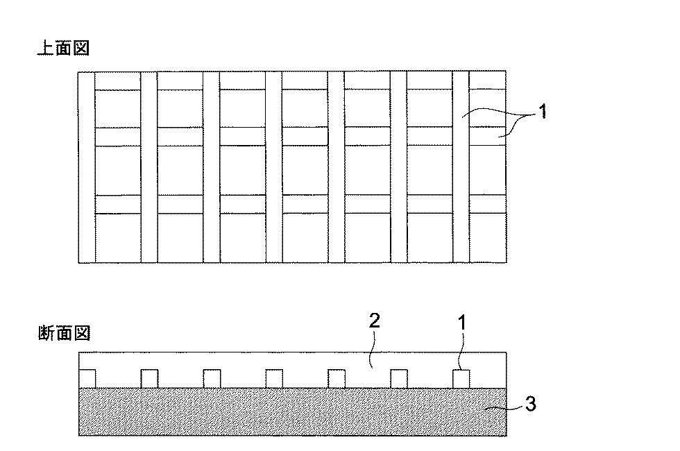
表1に示した結果から、透明電極TC−113〜TC−117に対して、透明電極TC−101〜112は、光透過性、導電性、膜強度に優れると共に、高温、高湿度環境下においても光透過性、導電性、膜強度の劣化が少なく、安定性に優れることがわかる。 From the results shown in Table 1, the transparent electrodes TC-101 to 112 are superior to the transparent electrodes TC-113 to TC-117 in terms of light transmittance, conductivity, and film strength, and in a high temperature and high humidity environment. It can be seen that there is little deterioration in light transmittance, conductivity, and film strength, and the stability is excellent.
実施例2
《有機ELデバイスの作製》
作製した透明電極基板を超純水で洗浄後、パターン辺長20mmの正方形タイル状透明パターン一個が中央に配置されるように30mm角に切り出し、アノード電極に用いて、以下の手順でそれぞれ有機ELデバイスを作製した。正孔輸送層以降は蒸着により形成した。透明電極TC−101〜TC−117を用い、それぞれ有機EL素子OEL−201〜OEL−217を作製した。
Example 2
<< Production of organic EL devices >>
The prepared transparent electrode substrate was washed with ultrapure water, cut into a 30 mm square so that one square tile-shaped transparent pattern with a pattern side length of 20 mm was placed in the center, and used for the anode electrode, respectively. A device was fabricated. The hole transport layer and subsequent layers were formed by vapor deposition. Organic EL elements OEL-201 to OEL-217 were produced using transparent electrodes TC-101 to TC-117, respectively.
市販の真空蒸着装置内の蒸着用るつぼの各々に、各層の構成材料を各々素子作製に必要量を充填した。蒸着用るつぼはモリブデン製又はタングステン製の抵抗加熱用材料で作製されたものを用いた。 Each crucible for vapor deposition in a commercially available vacuum vapor deposition apparatus was filled with a constituent material of each layer in a necessary amount for device production. The evaporation crucible used was made of a resistance heating material made of molybdenum or tungsten.
まず、正孔輸送層、有機発光層、正孔阻止層、電子輸送層からなる有機EL層を順次形成した。 First, an organic EL layer including a hole transport layer, an organic light emitting layer, a hole blocking layer, and an electron transport layer was sequentially formed.
〈正孔輸送層の形成〉
真空度1×10⁻⁴Paまで減圧した後、化合物1の入った前記蒸着用るつぼに通電して加熱し、蒸着速度0.1nm/秒で蒸着し、厚さ30nmの正孔輸送層を設けた。
<Formation of hole transport layer>
After depressurizing to a vacuum of 1 × 10 −4 Pa, the deposition crucible containing compound 1 was heated by energization, and deposited at a deposition rate of 0.1 nm / second to provide a 30 nm thick hole transport layer. It was.
〈有機発光層の形成〉
次に、以下の手順で各発光層を設けた。
<Formation of organic light emitting layer>
Next, each light emitting layer was provided in the following procedures.
形成した正孔輸送層上に、化合物2が13.0質量%、化合物3が3.7質量%、化合物5が83.3質量%になるように、化合物2、化合物3及び化合物5を蒸着速度0.1nm/秒で正孔輸送層と同じ領域に共蒸着し、発光極大波長が622nm、厚さ10nmの緑赤色燐光発光の有機発光層を形成した。
次いで、化合物4が10.0質量%、化合物5が90.0質量%になるように、化合物4及び化合物5を蒸着速度0.1nm/秒で緑赤色燐光発光の有機発光層と同じ領域に共蒸着し、発光極大波長が471nm、厚さ15nmの青色燐光発光の有機発光層を形成した。 Next, compound 4 and compound 5 are deposited in the same region as the organic light-emitting layer emitting green-red phosphorescence at a deposition rate of 0.1 nm / second so that compound 4 is 10.0% by mass and compound 5 is 90.0% by mass. Co-evaporation was performed to form a blue phosphorescent organic light emitting layer having an emission maximum wavelength of 471 nm and a thickness of 15 nm.
〈正孔阻止層の形成〉
更に、形成した有機発光層と同じ領域に、化合物6を膜厚5nmに蒸着して正孔阻止層を形成した。
<Formation of hole blocking layer>
Further, in the same region as the formed organic light emitting layer, the compound 6 was deposited to a thickness of 5 nm to form a hole blocking layer.
〈電子輸送層の形成〉
引き続き、形成した正孔阻止層と同じ領域に、CsFを膜厚比で10%になるように化合物6と共蒸着し、厚さ45nmの電子輸送層を形成した。
<Formation of electron transport layer>
Subsequently, in the same region as the formed hole blocking layer, CsF was co-evaporated with compound 6 so as to have a film thickness ratio of 10% to form an electron transport layer having a thickness of 45 nm.
〈カソード電極の形成〉
形成した電子輸送層の上に、透明電極を陽極として陽極外部取り出し端子及び15mm×15mmの陰極形成用材料としてAlを5×10⁻⁴Paの真空下にてマスク蒸着し、厚さ100nmの陽極を形成した。
<Formation of cathode electrode>
On the formed electron transport layer, a transparent electrode is used as an anode and an anode external takeout terminal and Al as a 15 mm × 15 mm cathode forming material are mask-deposited under a vacuum of 5 × 10 −4 Pa, and a 100 nm thick anode Formed.
更に、陰極及び陽極の外部取り出し端子が形成できるように、端部を除き陽極の周囲に接着剤を塗り、ポリエチレンテレフタレートを基材としAl2O3を厚さ300nmで蒸着した可撓性封止部材を貼合した後、熱処理で接着剤を硬化させ封止膜を形成し、発光エリア15mm×15mmの有機EL素子を作製した。 In addition, a flexible seal in which an adhesive is applied around the anode except for the end, and polyethylene terephthalate is used as a base material and Al 2 O 3 is deposited in a thickness of 300 nm so that external terminals for the cathode and anode can be formed. After pasting the members, the adhesive was cured by heat treatment to form a sealing film, and an organic EL device having a light emitting area of 15 mm × 15 mm was produced.
《有機EL素子の評価》
得られた有機EL素子について発光ムラ及び寿命を下記のように評価した。
<< Evaluation of organic EL elements >>
The obtained organic EL device was evaluated for light emission unevenness and lifetime as follows.
(発光均一性)
発光均一性は、KEITHLEY製ソースメジャーユニット2400型を用いて、直流電圧を有機EL素子に印加し発光させた。1000cd/m2で発光させた有機EL素子OEL−201〜OEL−217について、50倍の顕微鏡で各々の発光輝度ムラを観察した。又、有機EL素子OEL−201〜OEL−217をオーブンにて60%RH、80℃2時間加熱したのち、再び前記23±3℃、55±3%RHの環境下で1時間以上調湿した後、同様に発光均一性を観察した。
(Emission uniformity)
For light emission uniformity, a KEITHLEY source measure unit 2400 type was used to apply a DC voltage to the organic EL element to emit light. Regarding the organic EL elements OEL-201 to OEL-217 that emitted light at 1000 cd / m 2 , each light emission luminance unevenness was observed with a 50 × microscope. In addition, the organic EL elements OEL-201 to OEL-217 were heated in an oven at 60% RH and 80 ° C. for 2 hours, and then conditioned again in the environment of 23 ± 3 ° C. and 55 ± 3% RH for 1 hour or more. Thereafter, the emission uniformity was observed in the same manner.
◎:完全に均一発光しており、申し分ない
○:ほとんど均一発光しており、問題ない
△:部分的に若干発光ムラが見られるが、許容できる
×:全面にわたって発光ムラが見られ、許容できない
(寿命)
得られた有機EL素子の、初期の輝度を5000cd/m2で連続発光させて、電圧を固定して、輝度が半減するまでの時間を求めた。アノード電極をITOとした有機EL素子を上記と同様の方法で作製し、これに対する比率を求め、以下の基準で評価した。100%以上が好ましく、150%以上であることがより好ましい。
A: Completely uniform light emission, satisfactory O: Almost uniform light emission, no problem Δ: Some light emission unevenness is observed partially, but acceptable X: Light emission unevenness is observed over the entire surface, not acceptable (lifespan)
The obtained organic EL device was continuously emitted at an initial luminance of 5000 cd / m 2 , the voltage was fixed, and the time until the luminance was reduced by half was determined. An organic EL element having an anode electrode made of ITO was produced by the same method as described above, the ratio to this was determined, and evaluated according to the following criteria. 100% or more is preferable, and 150% or more is more preferable.
◎:150%以上
○:100〜150%未満
△:80〜100%未満
×:80%未満
評価の結果を表2に示す。
A: 150% or more B: 100 to less than 150% B: 80 to less than 100% X: less than 80% The results of evaluation are shown in Table 2.
表2から、比較の有機EL素子OEL−213〜OEL−217は80℃2時間の加熱後、発光均一性が著しく劣化するのに対し、本発明の有機EL素子OEL−201〜OEL−212の発光均一性は加熱後でも安定しており耐久性に優れることがわかる。 From Table 2, the comparative organic EL elements OEL-213 to OEL-217 are significantly deteriorated in light emission uniformity after heating at 80 ° C. for 2 hours, whereas the organic EL elements OEL-201 to OEL-212 of the present invention are significantly deteriorated. It can be seen that the light emission uniformity is stable even after heating and has excellent durability.
1 パターン状に形成された金属材料からなる第1導電層
2 本発明のバインダー樹脂と導電性ポリマーを含有する第2導電層
3 基材
DESCRIPTION OF SYMBOLS 1 1st conductive layer which consists of metal material formed in
Claims (4)
Priority Applications (1)
| Application Number | Priority Date | Filing Date | Title |
|---|---|---|---|
| JP2011109131A JP2012243401A (en) | 2011-05-16 | 2011-05-16 | Transparent conductive film and organic electroluminescent element |
Applications Claiming Priority (1)
| Application Number | Priority Date | Filing Date | Title |
|---|---|---|---|
| JP2011109131A JP2012243401A (en) | 2011-05-16 | 2011-05-16 | Transparent conductive film and organic electroluminescent element |
Publications (1)
| Publication Number | Publication Date |
|---|---|
| JP2012243401A true JP2012243401A (en) | 2012-12-10 |
Family
ID=47464936
Family Applications (1)
| Application Number | Title | Priority Date | Filing Date |
|---|---|---|---|
| JP2011109131A Withdrawn JP2012243401A (en) | 2011-05-16 | 2011-05-16 | Transparent conductive film and organic electroluminescent element |
Country Status (1)
| Country | Link |
|---|---|
| JP (1) | JP2012243401A (en) |
Cited By (3)
| Publication number | Priority date | Publication date | Assignee | Title |
|---|---|---|---|---|
| JP2016204643A (en) * | 2015-04-15 | 2016-12-08 | 国立大学法人山梨大学 | Conductive polymer composite, manufacturing method of conductive polymer composite, conductive polymer composite composition and thin film |
| JP2017048291A (en) * | 2015-09-01 | 2017-03-09 | テイカ株式会社 | Conductive polymer composition, dispersion liquid of the same, method for producing the dispersion liquid and application of the same |
| JP2017057267A (en) * | 2015-09-16 | 2017-03-23 | テイカ株式会社 | Conductive polymer composition and application thereof |
-
2011
- 2011-05-16 JP JP2011109131A patent/JP2012243401A/en not_active Withdrawn
Cited By (3)
| Publication number | Priority date | Publication date | Assignee | Title |
|---|---|---|---|---|
| JP2016204643A (en) * | 2015-04-15 | 2016-12-08 | 国立大学法人山梨大学 | Conductive polymer composite, manufacturing method of conductive polymer composite, conductive polymer composite composition and thin film |
| JP2017048291A (en) * | 2015-09-01 | 2017-03-09 | テイカ株式会社 | Conductive polymer composition, dispersion liquid of the same, method for producing the dispersion liquid and application of the same |
| JP2017057267A (en) * | 2015-09-16 | 2017-03-23 | テイカ株式会社 | Conductive polymer composition and application thereof |
Similar Documents
| Publication | Publication Date | Title |
|---|---|---|
| JP5741581B2 (en) | Transparent conductive film and organic electroluminescence element | |
| JP5987843B2 (en) | Composition for forming transparent electrode, transparent electrode, organic electronic device, and method for producing transparent electrode | |
| JP5888084B2 (en) | Transparent electrode for organic electronic device, method for producing transparent electrode for organic electronic device, and organic electronic device | |
| JP5880100B2 (en) | Manufacturing method of transparent electrode | |
| JP6024351B2 (en) | Conductive film, organic electroluminescence element, and method of manufacturing conductive film | |
| JP5655745B2 (en) | Transparent electrode and organic electroluminescence device | |
| JP5761058B2 (en) | Method for producing transparent conductive film and organic electroluminescence element | |
| JP5660121B2 (en) | Transparent conductive film and organic electroluminescence element | |
| JP5782855B2 (en) | Transparent electrode and organic electroluminescence device | |
| US20150311443A1 (en) | Method for producing transparent electrode and organic el element | |
| WO2013061967A1 (en) | Transparent conductive film and organic electroluminescent element | |
| JP2014229397A (en) | Method for manufacturing electroconductive film, electroconductive film, organic electronic element, and touch panel | |
| JP6003582B2 (en) | Manufacturing method of transparent electrode | |
| JP5750908B2 (en) | Method for producing transparent conductive film, transparent conductive film and organic electroluminescence element | |
| JP2012243401A (en) | Transparent conductive film and organic electroluminescent element | |
| JP6015764B2 (en) | Transparent conductive film and organic electroluminescence device | |
| JP2013218857A (en) | Transparent electrode, method for manufacturing transparent electrode, and organic electronic element including the transparent electrode | |
| JP2012054085A (en) | Method of preparing dispersion, transparent conductive film, method of forming transparent conductive film, and organic electroluminescence element | |
| JP2012138311A (en) | Transparent conductive film substrate and organic electroluminescent element | |
| JP5834954B2 (en) | Transparent conductive film and organic electroluminescence device | |
| JP2012248383A (en) | Transparent electrode and organic electronic element using the same | |
| JP5617539B2 (en) | Transparent conductive film substrate and organic electroluminescence element | |
| JP5741366B2 (en) | Manufacturing method of transparent electrode | |
| JP5494390B2 (en) | Transparent conductive film and organic electroluminescence element | |
| JP2012160391A (en) | Transparent conductive film and organic electroluminescent element |
Legal Events
| Date | Code | Title | Description |
|---|---|---|---|
| A300 | Application deemed to be withdrawn because no request for examination was validly filed |
Free format text: JAPANESE INTERMEDIATE CODE: A300 Effective date: 20140805 |