JP2012242585A - Display device, electronic apparatus, and driving method for display device - Google Patents
Display device, electronic apparatus, and driving method for display device Download PDFInfo
- Publication number
- JP2012242585A JP2012242585A JP2011112280A JP2011112280A JP2012242585A JP 2012242585 A JP2012242585 A JP 2012242585A JP 2011112280 A JP2011112280 A JP 2011112280A JP 2011112280 A JP2011112280 A JP 2011112280A JP 2012242585 A JP2012242585 A JP 2012242585A
- Authority
- JP
- Japan
- Prior art keywords
- drive
- pulse
- unit
- transistor
- display device
- Prior art date
- Legal status (The legal status is an assumption and is not a legal conclusion. Google has not performed a legal analysis and makes no representation as to the accuracy of the status listed.)
- Withdrawn
Links
Images
Abstract
Description
本明細書で開示する技術は、表示装置、電子機器、及び、表示装置の駆動方法に関する。 The technology disclosed in this specification relates to a display device, an electronic apparatus, and a method for driving the display device.
今日、表示素子(電気光学素子とも称される)を具備する画素回路(画素とも称される)を有する表示装置、表示装置を具備する電子機器が広く利用されている。画素の表示素子として、印加される電圧や流れる電流によって輝度が変化する電気光学素子を用いた表示装置がある。例えば、印加される電圧によって輝度が変化する電気光学素子としては液晶表示素子が代表例であり、流れる電流によって輝度が変化する電気光学素子としては、有機エレクトロルミネッセンス(Organic Electro Luminescence, 有機EL, Organic Light Emitting Diode, OLED;以下、有機ELと記す) 素子が代表例である。後者の有機EL素子を用いた有機EL表示装置は、画素の表示素子として、自発光素子である電気光学素子を用いたいわゆる自発光型の表示装置である。 Today, display devices including pixel circuits (also referred to as pixels) including display elements (also referred to as electro-optical elements) and electronic devices including the display devices are widely used. As a display element of a pixel, there is a display device using an electro-optical element whose luminance changes depending on an applied voltage or a flowing current. For example, a liquid crystal display element is a typical example of an electro-optical element whose luminance changes depending on an applied voltage, and an organic electroluminescence (Organic Electro Luminescence, Organic EL, Organic) (Light Emitting Diode, OLED; hereinafter referred to as “organic EL”) A typical example is an element. The organic EL display device using the latter organic EL element is a so-called self-luminous display device using an electro-optic element which is a self-luminous element as a pixel display element.
ところで、表示素子を用いた表示装置においては、その駆動方式として、単純(パッシブ)マトリクス方式とアクティブマトリクス方式とを採ることができる。但し、単純マトリクス方式の表示装置は、構造が単純であるものの、大型でかつ高精細の表示装置の実現が難しい等の問題がある。 By the way, in a display device using a display element, a simple (passive) matrix method and an active matrix method can be adopted as the driving method. However, although a simple matrix display device has a simple structure, there is a problem that it is difficult to realize a large and high-definition display device.
このため、近年、画素内部の表示素子に供給する画素信号を、同様に画素内部に設けた能動素子、例えば絶縁ゲート型電界効果トランジスタ(一般には、薄膜トランジスタ(Thin Film Transistor ;TFT)等のトランジスタをスイッチングトランジスタとして使用して制御するアクティブマトリクス方式の開発が盛んに行なわれている。 For this reason, in recent years, a pixel signal supplied to a display element in a pixel has been changed to an active element similarly provided in the pixel, for example, an insulated gate field effect transistor (generally a transistor such as a thin film transistor (TFT)). Active matrix systems that are used and controlled as switching transistors have been actively developed.
従来のアクティブマトリクス方式の表示装置は、プロセス変動により表示素子を駆動するトランジスタの閾値電圧や移動度がばらついてしまう。又、表示素子の特性が経時的に変動する。このような駆動用のトランジスタの特性ばらつきや表示素子等の画素回路を構成する素子の特性変動は、発光輝度に影響を与えてしまう。即ち、各画素に全て同一のレベルの映像信号を供給すれば、全画素が同一輝度で発光し、画面の一様性(ユニフォーミティ)が得られるはずであるが、駆動用のトランジスタの特性ばらつきや表示素子の特性変動により、画面のユニフォーミティが損なわれる。そこで、表示装置の画面全体に亘って発光輝度を均一に制御するため、各画素回路内でトランジスタや表示素子等の画素回路を構成する素子の特性ばらつき等に起因する表示むらを補正する技術が、例えば特許第4240059号公報や特許第4240068号公報に提案されている。 In a conventional active matrix display device, the threshold voltage and mobility of a transistor that drives a display element vary due to process variations. Further, the characteristics of the display element change with time. Such variations in the characteristics of the driving transistors and fluctuations in the characteristics of the elements constituting the pixel circuit, such as the display elements, affect the light emission luminance. In other words, if video signals of the same level are supplied to each pixel, all pixels should emit light with the same luminance and screen uniformity (uniformity) should be obtained. However, the characteristics of the driving transistors vary. Also, the uniformity of the screen is impaired due to the characteristic variation of the display element. Therefore, in order to uniformly control the light emission luminance over the entire screen of the display device, there is a technique for correcting display unevenness caused by characteristic variations of elements constituting a pixel circuit such as a transistor or a display element in each pixel circuit. For example, it is proposed in Japanese Patent No. 4240059 and Japanese Patent No. 4240068.
ここで、素子の特性むら(ばらつき及び経時変動の双方を含む)に起因する表示むらを改善する技術においては、各種の駆動パルスのタイミングによってトランジスタを制御して表示輝度を制御する。このため、駆動パルスの形状(幅、変化特性等)がばらつくと表示むらの原因となってしまう。 Here, in a technique for improving display unevenness due to element characteristic unevenness (including both variation and temporal variation), display luminance is controlled by controlling transistors according to timings of various drive pulses. For this reason, if the shape (width, change characteristics, etc.) of the drive pulse varies, it causes display unevenness.
したがって本開示の目的は、駆動パルスの形状(幅、変化特性等)がばらつくことに起因する表示むら現象を抑制することのできる技術を提供することにある。 Accordingly, an object of the present disclosure is to provide a technique capable of suppressing the display unevenness phenomenon caused by variations in the shape (width, change characteristics, etc.) of the drive pulse.
本開示の第1の態様に係る表示装置は、表示部と、保持容量と、映像信号と対応する駆動電圧を保持容量に書き込む書込トランジスタと、保持容量に書き込まれた駆動電圧に基づいて表示部を駆動する駆動トランジスタ、とを有する画素回路が所定の方向に配列されている画素部を備える。ここで、画素部には、所定の方向に配列されている各書込トランジスタと各駆動トランジスタの少なくとも一方を駆動するために駆動パルスを供給する駆動線が配されている。本開示の第1の態様に係る表示装置は、駆動線を選択する選択部と、駆動パルスの元になるパルス信号を生成するパルス生成部、とを更に備え、選択部は、パルス生成部で生成されたパルス信号に基づいて、複数の駆動線へ駆動パルスを供給する。本開示の第1の態様に係る表示装置の従属項に記載された各表示装置は、本開示の第1の態様に係る表示装置のさらなる有利な具体例を規定する。 The display device according to the first aspect of the present disclosure includes a display unit, a storage capacitor, a write transistor that writes a drive voltage corresponding to a video signal in the storage capacitor, and a display based on the drive voltage written in the storage capacitor. A pixel portion having a driving transistor for driving the portion and a pixel circuit arranged in a predetermined direction. Here, the pixel portion is provided with a drive line for supplying a drive pulse to drive at least one of the write transistors and the drive transistors arranged in a predetermined direction. The display device according to the first aspect of the present disclosure further includes a selection unit that selects a drive line and a pulse generation unit that generates a pulse signal that is a source of the drive pulse, and the selection unit is a pulse generation unit. Based on the generated pulse signal, a drive pulse is supplied to a plurality of drive lines. Each display device described in the dependent claims of the display device according to the first aspect of the present disclosure defines a further advantageous specific example of the display device according to the first aspect of the present disclosure.
本開示の第2の態様に係る電子機器は、表示部、保持容量、映像信号と対応する駆動電圧を保持容量に書き込む書込トランジスタ、及び、保持容量に書き込まれた駆動電圧に基づいて表示部を駆動する駆動トランジスタを具備した表示素子が配列された画素部と、画素部に供給される映像信号を生成する信号生成部、とを備える。ここで、画素部には、所定の方向に配列されている各書込トランジスタと各駆動トランジスタの少なくとも一方を駆動するために駆動パルスを供給する駆動線が配されている。本開示の第2の態様に係る電子機器は、駆動線を選択する選択部と、駆動パルスの元になるパルス信号を生成するパルス生成部、とを更に備え、選択部は、パルス生成部で生成されたパルス信号に基づいて、複数の駆動線へ駆動パルスを供給する。第2の態様に係る電子機器は、第1の態様に係る表示装置の従属項に記載された各技術・手法が同様に適用可能であり、それが適用された構成は、第2の態様に係る電子機器のさらなる有利な具体例を規定する。 An electronic apparatus according to a second aspect of the present disclosure includes a display unit, a storage capacitor, a write transistor that writes a drive voltage corresponding to a video signal to the storage capacitor, and a display unit based on the drive voltage written to the storage capacitor A pixel unit in which display elements each including a driving transistor for driving the pixel unit are arranged, and a signal generation unit that generates a video signal supplied to the pixel unit. Here, the pixel portion is provided with a drive line for supplying a drive pulse to drive at least one of the write transistors and the drive transistors arranged in a predetermined direction. The electronic device according to the second aspect of the present disclosure further includes a selection unit that selects a drive line and a pulse generation unit that generates a pulse signal that is a source of the drive pulse, and the selection unit is a pulse generation unit. Based on the generated pulse signal, a drive pulse is supplied to a plurality of drive lines. In the electronic device according to the second aspect, each technique and method described in the dependent claims of the display device according to the first aspect can be similarly applied, and the configuration to which the technique / method is applied is similar to the second aspect. Further advantageous specific examples of such electronic devices will be defined.
本開示の第3の態様に係る表示装置の駆動方法は、表示部、保持容量、映像信号と対応する駆動電圧を保持容量に書き込む書込トランジスタ、及び、保持容量に書き込まれた駆動電圧に基づいて表示部を駆動する駆動トランジスタを具備した画素回路が配列された画素部の各画素回路を駆動する方法であって、駆動パルスの元になるパルス信号を生成し、生成されたパルス信号に基づいて、複数の駆動線へ駆動パルスを供給する。第3の態様に係る表示装置の駆動方法は、第1の態様に係る表示装置の従属項に記載された各技術・手法が同様に適用可能であり、それが適用された構成は、第3の態様に係る表示装置の駆動方法のさらなる有利な具体例を規定する。 A display device driving method according to a third aspect of the present disclosure is based on a display unit, a storage capacitor, a writing transistor that writes a driving voltage corresponding to a video signal to the storage capacitor, and a driving voltage written in the storage capacitor. A method of driving each pixel circuit of a pixel portion in which a pixel circuit having a driving transistor for driving a display portion is arranged, generating a pulse signal that is a source of a driving pulse, and based on the generated pulse signal Then, a drive pulse is supplied to a plurality of drive lines. The technology and method described in the dependent claims of the display device according to the first aspect can be similarly applied to the driving method of the display device according to the third aspect. Further advantageous specific examples of the driving method of the display device according to the aspect will be defined.
要するに、本明細書で開示する技術では、駆動パルスの元になるパルス信号を駆動部とは別の箇所に設けられたパルス生成部で生成し、駆動部では、パルス生成部で生成されたパルス信号に基づいて、複数の駆動線へ駆動パルスを供給する。複数の駆動線に供給された駆動信号は同じパルス生成部で生成されたパルス信号に基づくので、各駆動パルスの間にはパルス形状(幅、変化特性等)のばらつきがないと云ってよく、駆動パルスの形状(幅、変化特性等)がばらつくことに起因する表示むら現象が抑制される。 In short, in the technology disclosed in this specification, a pulse signal that is a source of a drive pulse is generated by a pulse generation unit provided at a location different from the drive unit, and the drive unit generates a pulse generated by the pulse generation unit. Based on the signal, a drive pulse is supplied to a plurality of drive lines. Since drive signals supplied to a plurality of drive lines are based on pulse signals generated by the same pulse generation unit, it can be said that there is no variation in pulse shape (width, change characteristics, etc.) between the drive pulses. The display unevenness phenomenon due to the variation in the shape (width, change characteristics, etc.) of the drive pulse is suppressed.
第1の態様に係る表示装置、第2の態様に係る電子機器、第3の態様に係る表示装置の駆動方法によれば、駆動パルスの形状(幅、変化特性等)がばらつくことに起因する表示むら現象を抑制することができる。 According to the display device according to the first aspect, the electronic device according to the second aspect, and the driving method of the display device according to the third aspect, the shape (width, change characteristics, etc.) of the drive pulse varies. The display unevenness phenomenon can be suppressed.
以下、図面を参照して、本明細書で開示する技術の実施形態について詳細に説明する。各機能要素について形態別に区別する際にはアルファベット或いは“_n”(nは数字)或いはこれらの組合せの参照子を付して記載し、特に区別しないで説明する際にはこの参照子を割愛して記載する。図面においても同様である。 Hereinafter, embodiments of the technology disclosed in this specification will be described in detail with reference to the drawings. When distinguishing each functional element according to its form, an alphabet or “_n” (n is a number) or a combination of these is given as a reference, and this reference is omitted when it is not particularly distinguished. To be described. The same applies to the drawings.
説明は以下の順序で行なう。
1.全体概要
2.表示装置の概要
3.発光素子
4.駆動方法:基本
5.具体的な適用例:
駆動パルスの形状がばらつくことに起因する表示むら現象の対処
実施例1:同じパルス信号をスイッチ選択、走査線の最外部にパルス生成部
実施例2:同じパルス信号をスイッチ選択、走査線配列方向中間にパルス生成部
実施例3:パルス生成部で生成されたパルス信号を順次シフト
実施例4:電子機器への適用事例
The description will be made in the following order.
1.
Coping with display unevenness phenomenon due to variation in shape of drive pulse Example 1: Switch selection of same pulse signal, pulse generation unit at outermost part of scanning line Example 2: Switch selection of same pulse signal, direction of scanning line arrangement Pulse generator in the middle Example 3: Sequentially shifting the pulse signal generated in the pulse generator Example 4: Application example to electronic equipment
<全体概要>
本実施形態の構成において、表示装置、或いは、電子機器は、表示部と、保持容量と、映像信号と対応する駆動電圧を保持容量に書き込む書込トランジスタと、保持容量に書き込まれた駆動電圧に基づいて表示部を駆動する駆動トランジスタとを有する画素回路が所定の方向に配列されている画素部を備える。画素部には、所定の方向に配列されている各書込トランジスタと各駆動トランジスタの少なくとも一方を駆動するために駆動パルスを供給する駆動線(走査線)が配されており、この駆動線を選択する選択部を更に備える。又、表示装置、或いは、電子機器は、駆動パルスの元になるパルス信号を生成するパルス生成部を備えており、パルス生成部で生成されたパルス信号に基づいて選択部が複数の駆動線へ駆動パルスを供給する。駆動パルスの元になるパルス信号を駆動部とは別の箇所に設けられたパルス生成部で生成し、パルス生成部で生成されたパルス信号に基づいて駆動部が複数の駆動線へ駆動パルスを供給する。したがって、複数の駆動線に供給された駆動信号は同じパルス生成部で生成されたパルス信号に基づくので、各駆動パルスの間にはパルス形状(幅、変化特性等)のばらつきは実質的に発生せず、駆動パルスの形状(幅、変化特性等)がばらつくことに起因する表示むら現象を抑制することができる。
<Overview>
In the configuration of this embodiment, the display device or the electronic device uses the display unit, the storage capacitor, the write transistor that writes the drive voltage corresponding to the video signal in the storage capacitor, and the drive voltage written in the storage capacitor. A pixel portion having a driving transistor for driving the display portion based on the pixel portion is arranged in a predetermined direction. The pixel portion is provided with a drive line (scanning line) for supplying a drive pulse to drive at least one of the write transistors and the drive transistors arranged in a predetermined direction. A selection unit for selecting is further provided. In addition, the display device or the electronic apparatus includes a pulse generation unit that generates a pulse signal that is a source of the drive pulse, and the selection unit transfers the drive signal to a plurality of drive lines based on the pulse signal generated by the pulse generation unit. Supply drive pulses. A pulse signal that is the source of the drive pulse is generated by a pulse generation unit provided at a location different from the drive unit, and the drive unit sends drive pulses to a plurality of drive lines based on the pulse signal generated by the pulse generation unit. Supply. Therefore, since the drive signals supplied to a plurality of drive lines are based on the pulse signals generated by the same pulse generation unit, variations in pulse shape (width, change characteristics, etc.) are substantially generated between the drive pulses. In addition, the display unevenness phenomenon caused by the variation in the shape (width, change characteristics, etc.) of the drive pulse can be suppressed.
パルス生成部で生成されたパルス信号に基づいて複数の駆動線へ駆動部が駆動パルスを供給するので、パルス生成部の数は駆動線の総数よりも少なくてよい。この場合、全駆動線について1つのパルス生成部を設けることができるし、全駆動線の内の一部の複数の駆動線を一単位として、一単位ごとにパルス生成部を設けることもできる。 Since the drive unit supplies drive pulses to the plurality of drive lines based on the pulse signal generated by the pulse generation unit, the number of pulse generation units may be smaller than the total number of drive lines. In this case, one pulse generation unit can be provided for all the drive lines, and a pulse generation unit can be provided for each unit, with some of the drive lines as a unit.
パルス生成部の配置箇所としては、走査線の最外部に配置することもできるが、好ましくは、走査線の配列方向の中間部に配置する方がよい。パルス生成部から出力されるパルス信号の遅延量の差による弊害を小さくできるからである。因みに、全駆動線の内の一部の複数の駆動線の一単位ごとにパルス生成部を設ける場合には、その一単位ごとに、駆動線の配列方向における中間部にパルス生成部を配置すればよい。 The pulse generation unit may be arranged at the outermost part of the scanning line, but is preferably arranged at an intermediate part in the arrangement direction of the scanning line. This is because the adverse effects caused by the difference in the delay amount of the pulse signal output from the pulse generator can be reduced. Incidentally, when a pulse generator is provided for each unit of a plurality of drive lines of all the drive lines, the pulse generator is arranged in the intermediate part in the drive line arrangement direction for each unit. That's fine.
パルス生成部は、画素部の内部に設けることもできるし、画素部の外部に設けることもできる。画素部の外部に設けた方が、選択部(走査部)とパルス生成部とを一体的に造り込むことができる利点がある。画素部と選択部(走査部)とが別体とされる場合に好適な構成である。 The pulse generation unit can be provided inside the pixel unit or can be provided outside the pixel unit. Providing outside the pixel portion has an advantage that the selection portion (scanning portion) and the pulse generation portion can be integrally formed. This configuration is suitable when the pixel portion and the selection portion (scanning portion) are separated.
本実施形態の構成において、表示装置、或いは、電子機器は、選択部の駆動線の選択に基づき、パルス生成部で生成されたパルス信号を取り込んで、駆動線に供給するスイッチ回路、を駆動線ごとに有するスイッチ部を更に備える構成にすることができる。スイッチ回路としては、CMOSスイッチ等のトランスファーゲート構造を利用したものであるとよい。この場合、画素回路に入力される駆動パルスに関し、パネル内或いはパネル外で一括でパルス信号を生成した後に各CMOSスイッチ等で抜き出して走査線に供給する。「パネル内或いはパネル外で一括」であるので、パルス生成部は、各駆動線について、同じタイミングのパルス信号を生成するのがよい。仮に、各駆動線について異なるタイミングのパルス信号を生成する場合、スイッチ回路にパルスシフト機構等の対処が必要になる。スイッチ回路は、画素部の内部に設けることもできるし、画素部の外部に設けることもできる。画素部の外部に設けた方が、選択部(走査部)とスイッチ回路(更にはパルス生成部も)とを一体的に造り込むことができる利点がある。画素部と選択部(走査部)とが別体とされる場合に好適な構成である。 In the configuration of this embodiment, the display device or the electronic device uses a switching circuit that takes in the pulse signal generated by the pulse generation unit based on selection of the driving line of the selection unit and supplies the pulse signal to the driving line. It can be set as the structure further provided with the switch part which has for every. The switch circuit preferably uses a transfer gate structure such as a CMOS switch. In this case, regarding the drive pulses input to the pixel circuit, pulse signals are generated in a lump in the panel or outside the panel, and then extracted by each CMOS switch or the like and supplied to the scanning lines. Since it is “collectively within the panel or outside the panel”, the pulse generation unit may generate a pulse signal of the same timing for each drive line. If a pulse signal with different timing is generated for each drive line, a countermeasure such as a pulse shift mechanism is required for the switch circuit. The switch circuit can be provided inside the pixel portion or can be provided outside the pixel portion. Providing outside the pixel portion has an advantage that the selection portion (scanning portion) and the switch circuit (and also the pulse generation portion) can be integrally formed. This configuration is suitable when the pixel portion and the selection portion (scanning portion) are separated.
本実施形態の構成において、表示装置、或いは、電子機器は、選択部が、パルス生成部で生成されたパルス信号を一単位期間分ずつシフトして順に駆動線に供給するシフトレジスタ部を有する構成にすることもできる。これにより、一連の処理が一単位期間で完結される場合に限らず、一連の処理が複数の単位期間に亘る場合においても、駆動パルスの形状(幅、変化特性等)が行ごと或いは列ごとにばらつく度合いを緩和できる。論理回路を構成するトランジスタの特性ばらつきに起因する駆動パルスの形状のばらつきによる処理期間のばらつきが輝度むら(カラー表示の場合は色むら)として現れる現象を改善することができる。 In the configuration of the present embodiment, the display device or the electronic apparatus includes a shift register unit in which the selection unit shifts the pulse signal generated by the pulse generation unit by one unit period and sequentially supplies it to the drive line. It can also be. As a result, not only when a series of processing is completed in one unit period, but also when a series of processing spans a plurality of unit periods, the shape (width, change characteristics, etc.) of the drive pulse is set for each row or column. The degree of variation can be reduced. It is possible to improve a phenomenon in which variation in the processing period due to variation in the shape of the drive pulse due to variation in characteristics of the transistors forming the logic circuit appears as luminance unevenness (color unevenness in the case of color display).
駆動パルスは、例えば、書込トランジスタを介して映像信号を保持容量の一端に供給しつつ駆動トランジスタを介して保持容量に電流を供給する処理にも使用される。この処理は、書込トランジスタを介して映像信号を保持容量の一端に供給しつつ駆動トランジスタを介して保持容量に電流を供給する処理は、駆動トランジスタの移動度を補正する移動度補正処理に使用される。 The drive pulse is also used, for example, for a process of supplying a current to the storage capacitor via the drive transistor while supplying a video signal to one end of the storage capacitor via the write transistor. In this process, the process of supplying the current to the holding capacitor via the driving transistor while supplying the video signal to one end of the holding capacitor via the writing transistor is used for the mobility correction process for correcting the mobility of the driving transistor. Is done.
駆動パルスは、例えば、駆動トランジスタの閾値電圧のばらつきを補正するためにも使用される。前述の移動度補正との併用もあり得る。 The drive pulse is also used, for example, to correct variations in the threshold voltage of the drive transistor. A combination with the mobility correction described above is also possible.
デバイス構成としては、表示部がライン状或いは2次元マトリクス状に配列された画素部を備えるものでもよい。 As a device configuration, the display unit may include a pixel unit arranged in a line or a two-dimensional matrix.
表示部としては、例えば、有機エレクトロルミネッセンス発光部、無機エレクトロルミネッセンス発光部、LED発光部、半導体レーザー発光部等の自発光型の発光部を具備した発光素子を用いることができ、特に、有機エレクトロルミネッセンス発光部であるとよい。 As the display unit, for example, a light emitting element including a self-emitting type light emitting unit such as an organic electroluminescent light emitting unit, an inorganic electroluminescent light emitting unit, an LED light emitting unit, a semiconductor laser light emitting unit, etc. can be used. It is good that it is a luminescence light emitting part.
<表示装置の概要>
以下の説明においては、対応関係の理解を容易にするため、回路構成部材の抵抗値や容量値(静電容量、キャパシタンス)等は、その部材に付されている符号と同一符号で示すことがある。
<Outline of display device>
In the following description, in order to facilitate understanding of the correspondence relationship, the resistance value and the capacitance value (capacitance, capacitance), etc., of the circuit constituent member may be indicated by the same reference numerals as those attached to the member. is there.
[基本]
先ず、発光素子を備えた表示装置の概要について説明する。以下の回路構成の説明においては、「電気的に接続」を単に「接続」と記載するし、この「電気的に接続」は、特段の明示のない限り、直接に接続されることに限らず、他のトランジスタ(スイッチングトランジスタが典型例である)その他の電気素子(能動素子に限らず受動素子でもよい)を介して接続されることも含む。
[Basic]
First, an outline of a display device including a light emitting element will be described. In the following description of the circuit configuration, “electrically connected” is simply referred to as “connected”, and this “electrically connected” is not limited to being directly connected unless otherwise specified. It is also included that they are connected via other transistors (a switching transistor is a typical example) or other electrical elements (not limited to active elements but may be passive elements).
表示装置は、複数の画素回路(或いは単に画素とも称することもある)を備えている。各画素回路は、発光部と発光部を駆動する駆動回路とを具備する表示素子(電気光学素子)を有する。表示部としては、例えば、有機エレクトロルミネッセンス発光部、無機エレクトロルミネッセンス発光部、LED発光部、半導体レーザー発光部等の自発光型の発光部を具備した発光素子を用いることができる。尚、表示素子の発光部を駆動する方式としては定電流駆動型を採用するが、原理的には、定電流駆動型に限らず定電圧駆動型でもよい。 The display device includes a plurality of pixel circuits (or simply referred to as pixels). Each pixel circuit includes a display element (electro-optical element) including a light emitting unit and a drive circuit that drives the light emitting unit. As the display unit, for example, a light emitting element including a self-luminous light emitting unit such as an organic electroluminescence light emitting unit, an inorganic electroluminescence light emitting unit, an LED light emitting unit, a semiconductor laser light emitting unit, or the like can be used. Note that a constant current drive type is adopted as a method for driving the light emitting portion of the display element, but in principle, the constant current drive type is not limited to the constant current drive type.
以下に説明する例においては、発光素子として、有機エレクトロルミネッセンス発光部を備えている場合で説明する。より詳細には、発光素子は、駆動回路と、駆動回路に接続された有機エレクトロルミネッセンス発光部(発光部ELP)とが積層された構造を有する有機エレクトロルミネッセンス素子(有機EL素子)である。 In the example described below, a case where an organic electroluminescence light emitting unit is provided as a light emitting element will be described. More specifically, the light emitting element is an organic electroluminescent element (organic EL element) having a structure in which a driving circuit and an organic electroluminescent light emitting part (light emitting part ELP) connected to the driving circuit are stacked.
発光部ELPを駆動するための駆動回路として各種の回路があるが、画素回路としては、5Tr/1C型、4Tr/1C型、3Tr/1C型、或いは2Tr/1C型等の駆動回路を備えた構成にすることができる。「αTr/1C型」におけるαはトランジスタの数を意味し、「1C」は容量部が1つの保持容量Ccs(キャパシタ)を具備することを意味する。駆動回路を構成する各トランジスタは、好適には、全てがnチャネル型のトランジスタから構成されているのが好ましいが、これには限らず、場合によっては、一部のトランジスタをpチャネル型としてもよい。尚、半導体基板等にトランジスタを形成した構成とすることもできる。駆動回路を構成するトランジスタの構造は、特に限定するものではなく、MOS型FETを代表例とする絶縁ゲート型電界効果トランジスタ(一般には、薄膜トランジスタ(Thin Film Transistor ;TFT))を使用できる。更には、駆動回路を構成するトランジスタはエンハンスメント型とデプレッション型の何れでもよいし、又、シングルゲート型とデュアルゲート型の何れでもよい。 There are various types of driving circuits for driving the light emitting unit ELP, and the pixel circuit includes a driving circuit of 5Tr / 1C type, 4Tr / 1C type, 3Tr / 1C type, or 2Tr / 1C type. Can be configured. In the “αTr / 1C type”, α means the number of transistors, and “1C” means that the capacitor portion has one holding capacitor C cs (capacitor). The transistors constituting the drive circuit are preferably all n-channel transistors. However, the present invention is not limited to this, and in some cases, some transistors may be p-channel transistors. Good. Note that a transistor may be formed on a semiconductor substrate or the like. The structure of the transistor constituting the drive circuit is not particularly limited, and an insulated gate field effect transistor (typically, a thin film transistor (TFT)) typified by a MOS FET can be used. Further, the transistor constituting the driver circuit may be either an enhancement type or a depletion type, and may be either a single gate type or a dual gate type.
何れの構成においても、表示装置は、基本的には、最小の構成要素として2Tr/1C型と同様に、発光部ELP、駆動トランジスタTRD、書込トランジスタTRW(サンプリングトランジスタとも称される)、少なくとも書込走査部を具備する垂直走査部、信号出力部の機能を持つ水平駆動部、保持容量Ccsを備える。各走査部は、駆動線(走査線)を選択する選択部の一例である。好ましくは、ブートストラップ回路を構成するべく、駆動トランジスタTRDの制御入力端(ゲート端)と主電極端(ソース/ドレイン領域)の一方(典型的にはソース端)との間に保持容量Ccsが接続される。駆動トランジスタTRDは、主電極端の一方が発光部ELPと接続され、主電極端の他方は電源線PWLと接続される。電源線PWLには、電源回路或いは電源電圧用の走査回路等から電源電圧(定常電圧或いはパルス状の電圧)が供給される。 In any configuration, the display device basically has a light emitting unit ELP, a drive transistor TR D , and a write transistor TR W (also referred to as a sampling transistor) as in the 2Tr / 1C type as the minimum components. A vertical scanning unit including at least a writing scanning unit, a horizontal driving unit having a function of a signal output unit, and a holding capacitor C cs . Each scanning unit is an example of a selection unit that selects a drive line (scanning line). Preferably, in order to form a bootstrap circuit, a storage capacitor C is provided between the control input terminal (gate terminal) of the driving transistor TR D and one (typically the source terminal) of the main electrode terminal (source / drain region). cs is connected. Driving transistor TR D, one main electrode terminal is connected to the light emitting unit ELP, the other main electrode terminal is connected to the power supply line PWL. A power supply voltage (steady voltage or pulsed voltage) is supplied to the power supply line PWL from a power supply circuit or a scanning circuit for power supply voltage.
水平駆動部は、発光部ELPにおける輝度を制御するための映像信号Vsigや閾値補正等に使用される基準電位(1種とは限らない)を表す広義の映像信号VSを映像信号線DTL(データ線とも称される)に供給する。書込トランジスタTRWは、主電極端の一方が映像信号線DTLに接続され、主電極端の他方が駆動トランジスタTRDの制御入力端に接続される。書込走査部は書込トランジスタTRWをオン/オフ制御する制御パルス(書込駆動パルスWS)を書込走査線WSLを介して書込トランジスタTRWの制御入力端に供給する。書込トランジスタTRWの主電極端の他端と駆動トランジスタTRDの制御入力端と保持容量Ccsの一端との接続点を第1ノードND1と称し、駆動トランジスタTRDの主電極端の一方と保持容量Ccsの他端との接続点を第2ノードND2と称する。各走査線は、駆動パルスを画素回路を構成するトランジスタに供給する駆動線の一例である。 The horizontal drive unit displays a video signal V sig for controlling the luminance in the light emitting unit ELP, a video signal VS in a broad sense representing a reference potential (not limited to one type) used for threshold correction, and the like as a video signal line DTL ( Data line). Write transistor TR W is one of the main electrode terminal connected to the video signal line DTL, the other main electrode terminal connected to the control input terminal of the drive transistor TR D. Write scanner supplies a control input terminal of the write transistor TR W control pulse for turning on / off control of the write transistor TR W (write drive pulse WS) via a writing scanning line WSL. A connection point between the other end of the main electrode end of the write transistor TR W , the control input end of the drive transistor TR D , and one end of the storage capacitor C cs is referred to as a first node ND 1 , and is connected to the main electrode end of the drive transistor TR D. A connection point between one end and the other end of the storage capacitor C cs is referred to as a second node ND 2 . Each scanning line is an example of a driving line that supplies a driving pulse to a transistor included in the pixel circuit.
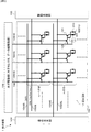
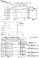
[構成例]
図1及び図2は、本開示に係る表示装置の一実施形態であるアクティブマトリクス型表示装置の一構成例の概略を示すブロック図である。図1は、一般的なアクティブマトリクス型表示装置の構成の概略を示すブロック図であり、図2は、そのカラー画像表示対応の場合の概略を示すブロック図である。
[Configuration example]
1 and 2 are block diagrams illustrating an outline of a configuration example of an active matrix display device that is an embodiment of a display device according to the present disclosure. FIG. 1 is a block diagram showing an outline of the configuration of a general active matrix display device, and FIG. 2 is a block diagram showing an outline in the case of color image display.
図1に示すように、表示装置1は、複数の表示素子としての有機EL素子(図示せず)を持った画素回路10(画素とも称される)が表示アスペクト比である縦横比がX:Y(例えば9:16)の有効映像領域を構成するように配置された表示パネル部100と、この表示パネル部100を駆動制御する種々のパルス信号を発するパネル制御部の一例である駆動信号生成部200(いわゆるタイミングジェネレータ)と、映像信号処理部220を備えている。駆動信号生成部200と映像信号処理部220とは、1チップのIC(Integrated Circuit;半導体集積回路)に内蔵され、本例では、表示パネル部100の外部に配置されている。
As shown in FIG. 1, the
尚、製品形態としては、図示のように、表示パネル部100、駆動信号生成部200、及び映像信号処理部220の全てを備えたモジュール(複合部品)形態の表示装置1として提供されることに限らず、例えば、表示パネル部100のみで表示装置1として提供すしてもよい。又、表示装置1は、封止された構成のモジュール形状のものをも含む。例えば、画素アレイ部102に透明なガラス等の対向部に貼り付けられて形成された表示モジュールが該当する。透明な対向部には、カラーフィルタ、保護膜、遮光膜等が設けられてもよい。表示モジュールには、外部から画素アレイ部102への映像信号Vsigや各種の駆動パルスを入出力するための回路部やFPC(フレキシブルプリントサーキット)等が設けられていてもよい。
As shown in the figure, the product form is provided as a
このような表示装置1は、様々な電子機器、例えば半導体メモリやミニディスク(MD)やカセットテープ等の記録媒体を利用した携帯型の音楽プレイヤー、デジタルカメラ、ノート型パーソナルコンピュータ、携帯電話等の携帯端末装置、ビデオカメラ等、電子機器に入力された映像信号や電子機器内で生成した映像信号を、静止画像や動画像(映像)として表示するあらゆる分野の電子機器の表示部に利用できる。
Such a
表示パネル部100は、基板101の上に、画素回路10がM行×N列のマトリクス状に配列された画素アレイ部102と、画素回路10を垂直方向に走査する垂直駆動部103と、画素回路10を水平方向に走査する水平駆動部106(水平セレクタ或いはデータ線駆動部とも称される)と、各駆動部(垂直駆動部103及び水平駆動部106)と外部回路とのインタフェースをとるインタフェース部130(IF)と、外部接続用の端子部108(パッド部)等が集積形成されている。即ち、垂直駆動部103や水平駆動部106やインタフェース部130等の周辺駆動回路が、画素アレイ部102と同一の基板101上に形成された構成となっている。第m行目(m=1、2、3、…、M)、第n列(n=1、2、3、…、N)に位置する発光素子(画素回路10)を、図では10_n,mで示している。
The display panel unit 100 includes a
インタフェース部130は、垂直駆動部103と外部回路とのインタフェースをとる垂直IF部133と、水平駆動部106と外部回路とのインタフェースをとる水平IF部136を有する。
The interface unit 130 includes a vertical IF
垂直駆動部103と水平駆動部106とで、信号電位の保持容量への書込みや、閾値補正動作や、移動度補正動作や、ブートストラップ動作を制御する制御部109が構成される。この制御部109とインタフェース部130(垂直IF部133や水平IF部136)を含めて、画素アレイ部102の画素回路10を駆動制御する駆動制御回路を構成している。
The
2Tr/1C型とする場合であれば、垂直駆動部103は、書込走査部(ライトスキャナWS;Write Scan)や電源供給能力を有する電源スキャナとして機能する駆動走査部(ドライブスキャナDS;Drive Scan)を有する。画素アレイ部102は、一例として、図示する左右方向の一方側もしくは両側から垂直駆動部103で駆動され、かつ図示する上下方向の一方側もしくは両側から水平駆動部106で駆動されるようになっている。
In the case of the 2Tr / 1C type, the
端子部108には、表示装置1の外部に配された駆動信号生成部200から、種々のパルス信号が供給される。同様に、映像信号処理部220から映像信号Vsigが供給される。カラー表示対応の場合には、色別(本例ではR(赤)、G(緑)、B(青)の3原色)の映像信号Vsig_R、映像信号Vsig_G、映像信号Vsig_Bが供給される。
Various pulse signals are supplied to the
一例としては、垂直駆動用のパルス信号として、垂直方向の走査開始パルスの一例であるシフトスタートパルスSP(図はSPDS、SPWSの2種)や垂直走査クロックCK(図はCKDS、CKWSの2種)、必要に応じて位相反転した垂直走査クロックxCK(図はxCKDS、xCKWSの2種)、並びに特定タイミングのパルス出力を指示するイネーブルパルス等の必要なパルス信号が供給される。水平駆動用のパルス信号として、水平方向の走査開始パルスの一例である水平スタートパルスSPHや水平走査クロックCKH、必要に応じて位相反転した水平走査クロックxCKH、並びに特定タイミングのパルス出力を指示するイネーブルパルス等の必要なパルス信号が供給される。 As an example, as a pulse signal for vertical driving, a shift start pulse SP (two types of SPDS and SPWS in the figure) and a vertical scanning clock CK (two types of CKDS and CKWS in the figure) are examples of a vertical scanning start pulse. ), Necessary pulse signals such as a vertical scanning clock xCK (two types of xCKDS and xCKWS in the figure) whose phases are inverted as necessary, and an enable pulse for instructing a pulse output at a specific timing are supplied. As horizontal drive pulse signals, horizontal start pulse SPH, which is an example of a horizontal scan start pulse, horizontal scan clock CKH, horizontal scan clock xCKH whose phase is reversed as necessary, and enable to instruct pulse output at a specific timing Necessary pulse signals such as pulses are supplied.
端子部108の各端子は、配線109を介して、垂直駆動部103や水平駆動部106に接続される。例えば、端子部108に供給された各パルスは、必要に応じて図示を割愛したレベルシフタ部で電圧レベルを内部的に調整した後、バッファを介して垂直駆動部103の各部や水平駆動部106に供給される。
Each terminal of the
画素アレイ部102は、図示を割愛するが(詳細は後述する)、表示素子としての有機EL素子に対して画素トランジスタが設けられた画素回路10が行列状に2次元配置され、画素配列に対して行ごとに垂直走査線SCLが配線されるとともに、列ごとに映像信号線DTLが配線された構成となっている。つまり、画素回路10は、垂直走査線SCLを介して直駆動部103と接続され、又、映像信号線DTLを介して水平駆動部106と接続されている。具体的には、マトリクス状に配列された各画素回路10に対しては、垂直駆動部103によって駆動パルスで駆動されるn行分の垂直走査線SCL_1〜SCL_nが画素行ごとに配線される。垂直駆動部103は、論理ゲートの組合せ(ラッチやシフトレジスタ等も含む)によって構成され、画素アレイ部102の各画素回路10を行単位で選択する、即ち、駆動信号生成部200から供給される垂直駆動系のパルス信号に基づき、垂直走査線SCLを介して各画素回路10を順次選択する。水平駆動部106は、論理ゲートの組合せ(ラッチやシフトレジスタ等も含む)によって構成され、画素アレイ部102の各画素回路10を列単位で選択する、即ち、駆動信号生成部200から供給される水平駆動系のパルス信号に基づき、選択された画素回路10に対し映像信号線DTLを介して映像信号VSの内の所定電位(例えば映像信号Vsigレベル)をサンプリングして保持容量Ccsに書き込ませる。
Although the
本実施形態の表示装置1は、線順次駆動や点順次駆動が可能になっており、垂直駆動部103の書込走査部104及び駆動走査部105は線順次で(つまり行単位で)で画素アレイ部102を走査するとともに、これに同期して水平駆動部106が、画像信号を、1水平ライン分を同時に(線順次の場合)、或いは画素単位で(点順次の場合)、画素アレイ部102に書き込む。
The
カラー画像表示対応をとるには、画素アレイ部102には、例えば図2に示すように、色別(本例ではR(赤)、G(緑)、B(青)の3原色)のサブピクセルとして画素回路10_R、画素回路10_G、画素回路10_Bを所定の配列順で縦ストライプ状に設ける。1組の色別のサブピクセルによりカラーの1画素が構成される。ここでは、サブピクセルレイアウトの一例として縦ストライプ状に各色のサブピクセルを配置したストライプ構造のものを示しているが、サブピクセルレイアウトはこのような配列例に限定されるものではない。サブピクセルを垂直方向にシフトさせた形態を採用してもよい。
In order to achieve color image display, the
尚、図1及び図2では、画素アレイ部102の一方側にのみ垂直駆動部103(詳しくはその構成要素)を配置する構成を示しているが、垂直駆動部103の各要素を画素アレイ部102を挟んで左右両側に配置する構成を採ることもできる。又、垂直駆動部103の各要素の一方と他方を左右の各別に配置する構成を採ることもできる。同様に、図1及び図2では、画素アレイ部102の一方側にのみ水平駆動部106を配置する構成を示しているが、画素アレイ部102を挟んで上下両側に水平駆動部106を配置する構成を採ることもできる。本例では、垂直シフトスタートパルス、垂直走査クロック、水平スタートパルス、水平走査クロック等のパルス信号を表示パネル部100の外部から入力する構成としているが、これらの各種のタイミングパルスを生成する駆動信号生成部200を表示パネル部100上に搭載することもできる。
1 and 2 show a configuration in which the vertical drive unit 103 (specifically, its constituent elements) is arranged only on one side of the
図示した構成は、表示装置の一形態を示したに過ぎず、製品形態としては、その他の形態をとることができる。即ち、表示装置は、画素回路10を構成する素子を行列状に配置した画素アレイ部と、画素アレイ部の周辺に配置され、各画素を駆動するための走査線と接続された走査部を主要部とする制御部と、制御部を動作させるための各種の信号を生成する駆動信号生成部や映像信号処理部を備えて装置の全体が構成されていればよい。製品形態としては、画素アレイ部と制御部とを同一の基体(例えばガラス基板)上に搭載した表示パネル部と駆動信号生成部や映像信号処理部を別体とする図示のような形態(パネル上配置構成と称する)の他に、表示パネル部には画素アレイ部を搭載し、それとは別基板(例えばフレキシブル基板)上に制御部や駆動信号生成部や映像信号処理部等の周辺回路を搭載する形態(周辺回路パネル外配置構成と称する)を採ることができる。又、画素アレイ部と制御部とを同一の基体上に搭載して表示パネル部を構成するパネル上配置構成の場合、画素アレイ部のTFTを生成する工程にて同時に制御部(必要に応じて駆動信号生成部や映像信号処理部も)用の各トランジスタを生成する形態(トランジスタ一体構成と称する)と、COG(Chip On Glass)実装技術により画素アレイ部が搭載された基体上に制御部(必要に応じて駆動信号生成部や映像信号処理部も)用の半導体チップを直接実装する形態(COG搭載構成と称する)を採ることもできる。或いは又、表示パネル部(少なくとも画素アレイ部を備える)のみで表示装置として提供することもできる。
The illustrated configuration only shows one form of the display device, and the product form can take other forms. That is, the display device mainly includes a pixel array unit in which elements constituting the
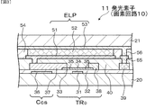
<発光素子>
図3は、駆動回路を備えた発光素子11(実質的には画素回路10)を説明する図である。ここで、図3は、発光素子11(画素回路10)の一部分の模式的な一部断面図である。図3では、絶縁ゲート型電界効果トランジスタは薄膜トランジスタ(TFT)であるとする。図示しないが、いわゆるバックゲート型の薄膜トランジスタ或いはMOS型のトランジスタを使用してもよい。
<Light emitting element>
FIG. 3 is a diagram for explaining the light emitting element 11 (substantially the pixel circuit 10) provided with a drive circuit. Here, FIG. 3 is a schematic partial cross-sectional view of a part of the light emitting element 11 (pixel circuit 10). In FIG. 3, it is assumed that the insulated gate field effect transistor is a thin film transistor (TFT). Although not shown, a so-called back gate type thin film transistor or MOS type transistor may be used.
発光素子11の駆動回路を構成する各トランジスタ及び容量部(保持容量Ccs)は支持体20上に形成され、発光部ELPは、例えば、層間絶縁層40を介して、駆動回路を構成する各トランジスタ及び保持容量Ccsの上方に形成されている。駆動トランジスタTRDの一方のソース/ドレイン領域は、発光部ELPに備えられたアノード電極に、コンタクトホールを介して接続されている。図3においては、駆動トランジスタTRDのみを図示する。書込トランジスタTRWやその他のトランジスタは隠れて見えない。発光部ELPは、例えば、アノード電極、正孔輸送層、発光層、電子輸送層、カソード電極等の周知の構成、構造を有する。
Each transistor and capacitor (retention capacitor C cs ) constituting the drive circuit of the light-emitting element 11 are formed on the
具体的には、駆動トランジスタTRDは、ゲート電極31、ゲート絶縁層32、半導体層33、半導体層33に設けられたソース/ドレイン領域35、及び、ソース/ドレイン領域35の間の半導体層33の部分が該当するチャネル形成領域34から構成されている。保持容量Ccsは、他方の電極36、ゲート絶縁層32の延在部から構成された誘電体層、及び、一方の電極37(第2ノードND2に相当する)から成る。ゲート電極31、ゲート絶縁層32の一部、及び、保持容量Ccsを構成する他方の電極36は、支持体20上に形成されている。駆動トランジスタTRDの一方のソース/ドレイン領域35は配線38に接続され、一方のソース/ドレイン領域35は一方の電極37に接続されている。駆動トランジスタTRD及び保持容量Ccs等は、層間絶縁層40で覆われており、層間絶縁層40上に、アノード電極51、正孔輸送層、発光層、電子輸送層、及び、カソード電極53から成る発光部ELPが設けられている。図3においては、正孔輸送層、発光層、及び、電子輸送層を1層52で表した。発光部ELPが設けられていない層間絶縁層40の部分の上には、第2層間絶縁層54が設けられ、第2層間絶縁層54及びカソード電極53上には透明な基板21が配置されており、発光層にて発光した光は、基板21を通過して、外部に出射される。一方の電極37とアノード電極51とは、層間絶縁層40に設けられたコンタクトホールによって接続されている。カソード電極53は、第2層間絶縁層54、層間絶縁層40に設けられたコンタクトホール56、コンタクトホール55を介して、ゲート絶縁層32の延在部上に設けられた配線39に接続されている。
Specifically, the drive transistor TR D includes a
[駆動方法]
発光部の駆動方法に関して、以下に説明する。理解を容易にするべく、画素回路10を構成する各トランジスタは、nチャネル型のトランジスタから構成されているとして説明する。又、発光部ELPは、アノード端が第2ノードND2に接続され、カソード端はカソード配線cath(その電位をカソード電位Vcathとする)に接続されるものとする。更には、ドレイン電流Idsの値の大小によって、発光部ELPにおける発光状態(輝度)が制御される。発光素子の発光状態においては、駆動トランジスタTRDの2つの主電極端(ソース/ドレイン領域)は、一方(発光部ELPのアノード側)がソース端(ソース領域)として働き、他方がドレイン端(ドレイン領域)として働く。表示装置は、カラー表示対応のものであり、(N/3)×M個の2次元マトリクス状に配列された画素回路10から構成され、カラー表示の一単位を成す1つの画素回路は、3つの副画素回路(赤色を発光する赤色発光画素回路10_R、緑色を発光する緑色発光画素回路10_G、青色を発光する青色発光画素回路10_B)から構成されているとする。各画素回路10を構成する発光素子は、線順次駆動されるとし、表示フレームレートをFR(回/秒)とする。即ち、第m行目(但し、m=1、2、3、…、M)に配列された(N/3)個の画素回路10、より具体的には、N個の画素回路10のそれぞれを構成する発光素子が同時に駆動される。換言すれば、1つの行を構成する各発光素子にあっては、その発光/非発光のタイミングは、それらが属する行単位で制御される。尚、1つの行を構成する各画素回路10について映像信号を書き込む処理は、全ての画素回路10について同時に映像信号を書き込む処理(同時書込み処理とも称する)でもよいし、画素回路10毎に順次映像信号を書き込む処理(順次書込み処理とも称する)でもよい。何れの書込み処理とするかは、駆動回路の構成に応じて適宜選択すればよい。
[Driving method]
A method for driving the light emitting unit will be described below. In order to facilitate understanding, each transistor constituting the
ここで、第m行目、第n列(但し、n=1、2、3、…、N)に位置する発光素子(画素回路10)に関する駆動動作を説明する。因みに、第m行目、第n列に位置する発光素子を、第(n、m)番目の発光素子或いは第(n、m)番目の発光素子画素回路と称する。第m行目に配列された各発光素子の水平走査期間(第m番目の水平走査期間)が終了するまでに、各種の処理(閾値補正処理、書込み処理、移動度補正処理、等)が行なわれる。尚、書込み処理や移動度補正処理は、第m番目の水平走査期間内に行なわれる必要がある。一方、駆動回路の種類によっては、閾値補正処理やこれに伴う前処理を第m番目の水平走査期間より先行して行なうことができる。 Here, a driving operation related to the light emitting element (pixel circuit 10) located in the m-th row and the n-th column (where n = 1, 2, 3,..., N) will be described. Incidentally, the light emitting element located in the mth row and the nth column is referred to as the (n, m) th light emitting element or the (n, m) th light emitting element pixel circuit. Various processes (threshold correction process, writing process, mobility correction process, etc.) are performed before the horizontal scanning period (m-th horizontal scanning period) of each light emitting element arranged in the m-th row is completed. It is. Note that the writing process and the mobility correction process need to be performed within the m-th horizontal scanning period. On the other hand, depending on the type of the drive circuit, the threshold correction processing and the preprocessing associated therewith can be performed prior to the mth horizontal scanning period.
前述の各種の処理が全て終了した後、第m行目に配列された各発光素子を構成する発光部を発光させる。尚、各種の処理が全て終了した後、直ちに発光部を発光させてもよいし、所定の期間(例えば、所定の行数分の水平走査期間)が経過した後に発光部を発光させてもよい。「所定の期間」は、表示装置の仕様や画素回路10(つまり駆動回路)の構成等に応じて、適宜設定すればよい。以下では説明の便宜のため、各種の処理終了後、直ちに発光部を発光させるものとする。第m行目に配列された各発光素子を構成する発光部の発光は、第(m+m’)行目に配列された各発光素子の水平走査期間の開始直前まで継続される。「m’」は、表示装置の設計仕様によって決定すればよい。即ち、或る表示フレームの第m行目に配列された各発光素子を構成する発光部の発光は、第(m+m’−1)番目の水平走査期間まで継続される。一方、第(m+m’)番目の水平走査期間の始期から、次の表示フレームにおける第m番目の水平走査期間内において書込み処理や移動度補正処理が完了するまで、第m行目に配列された各発光素子を構成する発光部は、原則として非発光状態を維持する。非発光状態の期間(非発光期間とも称する)を設けることにより、アクティブマトリクス駆動に伴う残像ボケが低減され、動画品位をより良好にすることができる。但し、各画素回路10(発光素子)の発光状態/非発光状態は、以上に説明した状態には限定されない。水平走査期間の時間長は、(1/FR)×(1/M)秒未満の時間長である。(m+m’)の値がMを越える場合、越えた分の水平走査期間は、次の表示フレームにおいて処理される。 After all the above-described various processes are completed, the light emitting units constituting the light emitting elements arranged in the m-th row are caused to emit light. In addition, after all the various processes are completed, the light emitting unit may emit light immediately, or the light emitting unit may emit light after a predetermined period (for example, a horizontal scanning period for a predetermined number of rows) has elapsed. . The “predetermined period” may be appropriately set according to the specifications of the display device, the configuration of the pixel circuit 10 (that is, the drive circuit), and the like. In the following, for convenience of explanation, it is assumed that the light emitting unit emits light immediately after completion of various processes. The light emission of the light emitting units constituting the light emitting elements arranged in the mth row is continued until just before the start of the horizontal scanning period of the light emitting elements arranged in the (m + m ′) th row. “M ′” may be determined according to the design specifications of the display device. That is, the light emission of the light emitting units constituting the light emitting elements arranged in the mth row of a certain display frame is continued until the (m + m′−1) th horizontal scanning period. On the other hand, from the beginning of the (m + m ′) th horizontal scanning period to the mth horizontal scanning period in the next display frame until the writing process and the mobility correction process are completed, they are arranged in the mth row. As a general rule, the light-emitting portion constituting each light-emitting element maintains a non-light-emitting state. By providing a non-light emitting period (also referred to as a non-light emitting period), afterimage blur caused by active matrix driving is reduced, and the quality of moving images can be improved. However, the light emission state / non-light emission state of each pixel circuit 10 (light emitting element) is not limited to the state described above. The time length of the horizontal scanning period is a time length of less than (1 / FR) × (1 / M) seconds. When the value of (m + m ′) exceeds M, the excess horizontal scanning period is processed in the next display frame.
トランジスタがオン状態(導通状態)にあるとは、主電極端間(ソース/ドレイン領域間)にチャネルが形成されている状態を意味し、一方の主電極端から他方の主電極端に電流が流れているか否かは問わない。トランジスタがオフ状態(非導通状態)にあるとは、主電極端間にチャネルが形成されていない状態を意味する。或るトランジスタの主電極端が他のトランジスタの主電極端に接続されているとは、或るトランジスタのソース/ドレイン領域と他のトランジスタのソース/ドレイン領域とが同じ領域を占めている形態を包含する。更には、ソース/ドレイン領域は、不純物を含有したポリシリコンやアモルファスシリコン等の導電性物質から構成することができるだけでなく、金属、合金、導電性粒子、これらの積層構造、有機材料(導電性高分子)から成る層から構成することができる。又、以下の説明で用いるタイミングチャートにおいて、各期間を示す横軸の長さ(時間長)は模式的なものであり、各期間の時間長の割合を示すものではない。 A transistor in an on state (conducting state) means a state in which a channel is formed between the main electrode ends (between the source / drain regions), and a current flows from one main electrode end to the other main electrode end. It doesn't matter whether it is flowing or not. The transistor being in an off state (non-conducting state) means a state in which no channel is formed between the main electrode ends. The main electrode end of a certain transistor is connected to the main electrode end of another transistor means that the source / drain region of a certain transistor and the source / drain region of another transistor occupy the same region. Includes. Furthermore, the source / drain regions can be composed not only of conductive materials such as polysilicon or amorphous silicon containing impurities, but also metals, alloys, conductive particles, their laminated structures, organic materials (conductive Polymer). In the timing chart used in the following description, the length of the horizontal axis (time length) indicating each period is a schematic one and does not indicate the ratio of the time length of each period.
画素回路10の駆動方法においては、前処理工程、閾値補正処理工程、映像信号書込み処理工程、移動度補正工程、発光工程を有する。前処理工程、閾値補正処理工程、映像信号書込み処理工程、及び、移動度補正工程を纏めて非発光工程とも称する。画素回路10の構成によっては映像信号書込み処理工程と移動度補正工程とを同時に行なうこともある。各工程について概説する。
The driving method of the
因みに、駆動トランジスタTRDは、発光素子の発光状態においては、以下の式(1)に従ってドレイン電流Idsを流すように駆動される。ドレイン電流Idsが発光部ELPを流れることで発光部ELPが発光する。更には、ドレイン電流Idsの値の大小によって、発光部ELPにおける発光状態(輝度)が制御される。発光素子の発光状態においては、駆動トランジスタTRDの2つの主電極端(ソース/ドレイン領域)は、一方(発光部ELPのアノード端側)がソース端(ソース領域)として働き、他方がドレイン端(ドレイン領域)として働く。説明の便宜のため、以下の説明において、駆動トランジスタTRDの一方の主電極端を単にソース端と称し、他方の主電極端を単にドレイン端と呼ぶ場合がある。尚、実効的な移動度μ、チャネル長L、チャネル幅W、制御電極端の電位(ゲート電位Vg)とソース端の電位(ソース電位Vs)との電位差(ゲート・ソース間電圧)Vgs、閾値電圧Vth、等価容量Cox((ゲート絶縁層の比誘電率)×(真空の誘電率)/(ゲート絶縁層の厚さ))、係数k≡(1/2)・(W/L)・Coxとする。 Incidentally, the drive transistor TR D is driven so that the drain current I ds flows according to the following formula (1) in the light emitting state of the light emitting element. When the drain current I ds flows through the light emitting unit ELP, the light emitting unit ELP emits light. Furthermore, the light emission state (luminance) in the light emitting unit ELP is controlled by the magnitude of the value of the drain current I ds . In the light emitting state of the light emitting element, one of the two main electrode ends (source / drain regions) of the driving transistor TR D serves as a source end (source region) while the other serves as a drain end. Work as (drain region). For convenience of description, in the following description, one main electrode end of the drive transistor TR D may be simply referred to as a source end, and the other main electrode end may be simply referred to as a drain end. Effective mobility μ, channel length L, channel width W, potential difference (gate-source voltage) V between control electrode end potential (gate potential V g ) and source end potential (source potential V s ) V gs , threshold voltage V th , equivalent capacitance C ox ((dielectric constant of gate insulating layer) × (dielectric constant of vacuum) / (thickness of gate insulating layer)), coefficient k≡ (1/2) · (W / L) · C ox .
Ids=k・μ・(Vgs−Vth)2 (1) I ds = k · μ · (V gs −V th ) 2 (1)
以下の説明では、特段の断りのない限り、発光部ELPの寄生容量の静電容量Celは、保持容量Ccsの静電容量Ccs及び駆動トランジスタTRDの寄生容量の一例であるゲート・ソース間の静電容量Cgsと比較して十分に大きな値であるとし、駆動トランジスタTRDのゲート端の電位(ゲート電位Vg)の変化に基づく駆動トランジスタTRDのソース領域(第2ノードND2)の電位(ソース電位Vs)の変化を考慮しない。 In the following description, unless otherwise specified, the capacitance C el of the parasitic capacitance of the light emitting unit ELP is an example of the capacitance C cs of the holding capacitor C cs and the parasitic capacitance of the driving transistor TR D. A source region (second node) of the drive transistor TR D based on a change in the potential (gate potential V g ) of the gate end of the drive transistor TR D is assumed to be a sufficiently large value compared with the capacitance C gs between the sources. ND 2 ) potential (source potential V s ) is not considered.
〔前処理工程〕
第1ノードND1と第2ノードND2との間の電位差が、駆動トランジスタTRDの閾値電圧Vthを越え、且つ、第2ノードND2と発光部ELPに備えられたカソード電極との間の電位差が、発光部ELPの閾値電圧VthELを越えないように、第1ノードND1に第1ノード初期化電圧(Vofs)を印加し、第2ノードND2に第2ノード初期化電圧(Vini)を印加する。例えば、発光部ELPにおける輝度を制御するための映像信号Vsigを0〜10ボルト、電源電圧Vccを20ボルト、駆動トランジスタTRDの閾値電圧Vthを3V、カソード電位Vcathを0ボルト、発光部ELPの閾値電圧VthELを3ボルトとする。この場合、駆動トランジスタTRDの制御入力端の電位(ゲート電位Vg、つまり第1ノードND1の電位)を初期化するための電位Vofsは0ボルト、駆動トランジスタTRDのソース端の電位(ソース電位Vsつまり第2ノードND2の電位)を初期化するための電位Viniは−10ボルトとする。
[Pretreatment process]
The potential difference between the first node ND 1 and the second node ND 2 exceeds the threshold voltage V th of the driving transistor TR D , and between the second node ND 2 and the cathode electrode provided in the light emitting unit ELP. The first node initialization voltage (V ofs ) is applied to the first node ND 1 and the second node initialization voltage is applied to the second node ND 2 so that the potential difference between the first node ND 1 and the threshold voltage V thEL does not exceed the threshold voltage V thEL. (V ini ) is applied. For example, the video signal V sig for controlling the luminance in the light emitting unit ELP is 0 to 10 volts, the power supply voltage V cc is 20 volts, the threshold voltage V th of the driving transistor TR D is 3 V, the cathode potential V cath is 0 volts, The threshold voltage V thEL of the light emitting unit ELP is 3 volts. In this case, the potential V ofs for initializing the potential of the control input terminal of the drive transistor TR D (gate potential V g , that is, the potential of the first node ND 1 ) is 0 volts, and the potential of the source terminal of the drive transistor TR D The potential V ini for initializing (the source potential V s, that is, the potential of the second node ND 2 ) is −10 volts.
〔閾値補正処理工程〕
第1ノードND1の電位を保った状態で、駆動トランジスタTRDにドレイン電流Idsを流して、第1ノードND1の電位から駆動トランジスタTRDの閾値電圧Vthを減じた電位に向かって第2ノードND2の電位を変化させる。この際には、前処理工程後の第2ノードND2の電位に駆動トランジスタTRDの閾値電圧Vthを加えた電圧を超える電圧(例えば発光時の電源電圧)を、駆動トランジスタTRDの主電極端の他方(第2ノードND2とは反対側)に印加する。この閾値補正処理工程において、第1ノードND1と第2ノードND2との間の電位差(換言すれば、駆動トランジスタTRDのゲート・ソース間電圧Vgs)が駆動トランジスタTRDの閾値電圧Vthに近づく程度は閾値補正処理の時間により左右される。よって、例えば閾値補正処理の時間を充分長く確保すれば第2ノードND2の電位は第1ノードND1の電位から駆動トランジスタTRDの閾値電圧Vthを減じた電位に達し、駆動トランジスタTRDはオフ状態となる。一方、例えば閾値補正処理の時間を短く設定せざるを得ない場合は、第1ノードND1と第2ノードND2との間の電位差が駆動トランジスタTRDの閾値電圧Vthより大きく、駆動トランジスタTRDはオフ状態とはならない場合がある。閾値補正処理の結果として、必ずしも駆動トランジスタTRDがオフ状態となることを要しない。尚、閾値補正処理工程においては、好ましくは、式(2)を満足するように電位を選択、決定しておくことで、発光部ELPが発光しないようにする。
[Threshold correction processing step]
While maintaining the potential of the first node ND 1, by supplying a drain current I ds to the drive transistor TR D, toward an electric potential obtained by subtracting the threshold voltage V th of the driving transistor TR D from the first node potential of ND 1 The potential of the second node ND 2 is changed. At this time, the pretreatment step after the second node ND 2 in a voltage exceeding the threshold voltage V th of the voltage obtained by adding the driving transistor TR D to the potential (e.g., power supply voltage during light emission), a main driving transistor TR D It is applied to the other electrode end (the side opposite to the second node ND 2 ). In the threshold value correction process, (in other words, the driving transistor TR gate-source voltage of the D V gs) the potential difference between the first node ND 1 and the second node ND 2 is the threshold voltage V of the drive transistor TR D The degree of approaching th depends on the threshold correction processing time. Thus, for example, if the threshold correction processing time is sufficiently long, the potential of the second node ND 2 reaches the potential obtained by subtracting the threshold voltage V th of the drive transistor TR D from the potential of the first node ND 1 , and the drive transistor TR D Is turned off. On the other hand, for example, when the threshold correction processing time must be set short, the potential difference between the first node ND 1 and the second node ND 2 is larger than the threshold voltage V th of the drive transistor TR D , and the drive transistor TR D may not be off. As a result of the threshold correction process, the drive transistor TR D does not necessarily have to be turned off. In the threshold value correction processing step, preferably, the light emitting unit ELP does not emit light by selecting and determining a potential so as to satisfy Expression (2).
(Vofs−Vth)<(VthEL+Vcath) (2) (V ofs -V th) <( V thEL + V cath) (2)
〔映像信号書込み処理工程〕
書込走査線WSLからの書込駆動パルスWSによりオン状態とされた書込トランジスタTRWを介して、映像信号線DTLから映像信号Vsigを第1ノードND1に印加し、第1ノードND1の電位をVsigへと上昇させる。この電第1ノードND1の電位変化分(ΔVin=Vsig−Vofs)に基づく電荷が、保持容量Ccs、発光部ELPの寄生容量Cel、駆動トランジスタTRDの寄生容量(例えばゲート・ソース間容量Cgs等)に振り分けられる。静電容量Celが、静電容量Ccs及びゲート・ソース間容量Cgsの静電容量Cgsと比較して十分に大きな値であれば、電位変化分(Vsig−Vofs)に基づく第2ノードND2の電位の変化は小さい。一般に、発光部ELPの寄生容量Celの静電容量Celは、保持容量Ccsの静電容量Ccs及びゲート・ソース間容量Cgsの静電容量Cgsよりも大きい。この点を勘案して、特段の必要がある場合を除き、第1ノードND1の電位変化により生ずる第2ノードND2の電位変化は考慮しない。この場合、ゲート・ソース間電圧Vgsは、式(3)で表すことができる。
[Video signal writing process]
The video signal V sig is applied from the video signal line DTL to the first node ND 1 via the write transistor TR W that is turned on by the write drive pulse WS from the write scanning line WSL, and the first node ND 1 Increase the potential of 1 to V sig . Charges based on the potential change (ΔV in = V sig −V ofs ) of the electric first node ND 1 are the holding capacitor C cs , the parasitic capacitance C el of the light emitting unit ELP, and the parasitic capacitance (eg, gate) of the driving transistor TR D. -The capacity between sources C gs etc.). Capacitance C el is, if sufficiently large value as compared with the capacitance C gs of the electrostatic capacitance C cs and the gate-source capacitance C gs, based on the potential variation (V sig -V ofs) The change in potential of the second node ND 2 is small. In general, the capacitance C el of the parasitic capacitance C el of the light emitting section ELP is larger than the capacitance C gs of the storage capacitor C cs of the electrostatic capacitance C cs and the gate-source capacitance C gs. In consideration of this point, the potential change of the second node ND 2 caused by the potential change of the first node ND 1 is not taken into account, unless otherwise required. In this case, the gate-source voltage V gs can be expressed by Equation (3).
Vg=Vsig
Vs ≒Vofs−Vth
Vgs≒Vsig−(Vofs−Vth) (3)
V g = V sig
V s ≒ V ofs -V th
V gs ≈ V sig − (V ofs −V th ) (3)
〔移動度補正処理工程〕
書込トランジスタTRWを介して映像信号Vsigを保持容量Ccsの一端に供給しつつ(つまり映像信号Vsigと対応する駆動電圧を保持容量Ccsに書き込みつつ)、駆動トランジスタTRDを介して保持容量Ccsに電流を供給する。例えば、書込走査線WSLからの書込駆動パルスWSによりオン状態とされた書込トランジスタTRWを介して映像信号線DTLから映像信号Vsigを第1ノードND1に供給した状態で、駆動トランジスタTRDに電源を供給しドレイン電流Idsを流して、第2ノードND2の電位を変化させ、所定期間経過後、書込トランジスタTRWをオフ状態にする。このときの第2ノードND2の電位変化分をΔV(=電位補正値、負帰還量)とする。移動度補正処理を実行するための所定期間は、表示装置の設計の際、設計値として予め決定しておけばよい。尚、この際には、好ましくは、式(2A)を満足するように移動度補正期間を決定する。こうすることで、移動度補正期間に発光部ELPが発光することはない。
[Mobility correction process]
While supplying the video signal V sig to one end of the holding capacitor C cs via the write transistor TR W (that is, while writing the drive voltage corresponding to the video signal V sig to the holding capacitor C cs ), via the drive transistor TR D Current is supplied to the holding capacitor C cs . For example, the drive is performed in a state where the video signal V sig is supplied from the video signal line DTL to the first node ND 1 via the write transistor TR W turned on by the write drive pulse WS from the write scanning line WSL. Power is supplied to the transistor TR D and the drain current I ds flows to change the potential of the second node ND 2 , and after a predetermined period, the write transistor TR W is turned off. The change in potential of the second node ND 2 at this time is represented by ΔV (= potential correction value, negative feedback amount). The predetermined period for executing the mobility correction process may be determined in advance as a design value when designing the display device. In this case, the mobility correction period is preferably determined so as to satisfy the formula (2A). By doing so, the light emitting unit ELP does not emit light during the mobility correction period.
(Vofs−Vth+ΔV)<(VthEL+Vcath) (2A) (V ofs −V th + ΔV) <(V thEL + V cath ) (2A)
駆動トランジスタTRDの移動度μの値が大きい場合は電位補正値ΔVは大きくなり、移動度μの値が小さい場合は電位補正値ΔVは小さくなる。このときの駆動トランジスタTRDのゲート・ソース間電圧Vgs(つまり第1ノードND1と第2ノードND2との電位差)は、式(4)で表すことができる。ゲート・ソース間電圧Vgsは発光時の輝度を規定するが、電位補正値ΔVは駆動トランジスタTRDのドレイン電流Idsに比例し、ドレイン電流Idsは移動度μに比例するので、結果的には、移動度μが大きいほど電位補正値ΔVが大きくなるので、画素回路10ごとの移動度μのばらつきを取り除くことができる。
When the value of mobility μ of the driving transistor TR D is large, the potential correction value ΔV is large, and when the value of mobility μ is small, the potential correction value ΔV is small. The gate-source voltage V gs (that is, the potential difference between the first node ND 1 and the second node ND 2 ) of the driving transistor TR D at this time can be expressed by Expression (4). Although the gate-source voltage V gs defines the luminance at the time of light emission, the potential correction value ΔV is proportional to the drain current I ds of the driving transistor TR D and the drain current I ds is proportional to the mobility μ. Since the potential correction value ΔV increases as the mobility μ increases, variations in the mobility μ for each
Vgs≒Vsig−(Vofs−Vth)−ΔV (4) V gs ≈ V sig − (V ofs −V th ) −ΔV (4)
〔発光工程〕
書込走査線WSLからの書込駆動パルスWSにより書込トランジスタTRWをオフ状態とすることにより第1ノードND1を浮遊状態とし、駆動トランジスタTRDに電源を供給して駆動トランジスタTRDを介して、駆動トランジスタTRDのゲート・ソース間電圧Vgs(第1ノードND1と第2ノードND2との間の電位差)に応じた電流Idsを発光部ELPに流すことにより発光部ELPを駆動して発光させる。
[Light emission process]
The first node ND 1 in a floating state by the OFF state of the writing transistor TR W by the write drive pulse WS from the write scanning line WSL, a driving transistor TR D to supply power to the driving transistor TR D The current I ds corresponding to the gate-source voltage V gs (potential difference between the first node ND 1 and the second node ND 2 ) of the driving transistor TR D is caused to flow through the light emitting unit ELP. To emit light.
〔駆動回路の構成による相違点〕
ここで、それぞれ典型的な、5Tr/1C型、4Tr/1C型、3Tr/1C型、2Tr/1C型での相違点は以下の通りである。5Tr/1C型では、駆動トランジスタTRDの電源側の主電極端と電源回路(電源部)との間に接続された第1トランジスタTR1(発光制御トランジスタ)と、第2ノード初期化電圧を印加する第2トランジスタTR2と、第1ノード初期化電圧を印加する第3トランジスタTR3とを設ける。第1トランジスタTR1、第2トランジスタTR2、第3トランジスタTR3は何れもスイッチングトランジスタである。第1トランジスタTR1は、発光期間にオン状態としておき、オフ状態にして非発光期間に入り、その後の閾値補正期間に一度オン状態にし、更に移動度補正期間以降(次の発光期間も)オン状態とする。第2トランジスタTR2は、第2ノードの初期化期間にのみオン状態としそれ以外はオフ状態とする。第3トランジスタTR3は、第1ノードの初期化期間から閾値補正期間に亘ってのみオン状態としそれ以外はオフ状態とする。書込トランジスタTRWは、映像信号書込み処理期間から移動度補正処理期間に亘ってオン状態とされ、それ以外はオフ状態とされる。
[Differences due to drive circuit configuration]
Here, the differences between the typical 5Tr / 1C type, 4Tr / 1C type, 3Tr / 1C type, and 2Tr / 1C type are as follows. In the 5Tr / 1C type, a first transistor TR 1 (light emission control transistor) connected between the main electrode end on the power supply side of the drive transistor TR D and the power supply circuit (power supply unit), and a second node initialization voltage A second transistor TR 2 to be applied and a third transistor TR 3 to apply a first node initialization voltage are provided. The first transistor TR 1 , the second transistor TR 2 , and the third transistor TR 3 are all switching transistors. The first transistor TR 1 is turned on during the light emission period, is turned off, enters the non-light emission period, is turned on once during the subsequent threshold correction period, and is turned on after the mobility correction period (also in the next light emission period). State. The second transistor TR 2 is turned on only during the initialization period of the second node, and is turned off otherwise. The third transistor TR 3 is turned on only during the threshold correction period from the initialization period of the first node, and is otherwise turned off. The writing transistor TR W is turned on from the video signal writing processing period to the mobility correction processing period, and is otherwise turned off.
4Tr/1C型では、5Tr/1C型から、第1ノード初期化電圧を印加する第3トランジスタTR3が省略され、第1ノード初期化電圧は映像信号線DTLから映像信号Vsigと時分割で供給される。第1ノードの初期化期間に第1ノード初期化電圧を映像信号線DTLから第1ノードに供給するべく、書込トランジスタTRWは第1ノードの初期化期間にもオン状態とされる。典型的には、書込トランジスタTRWは、第1ノードの初期化期間から移動度補正処理期間に亘ってオン状態とされ、それ以外はオフ状態とされる。 In the 4Tr / 1C type, the third transistor TR 3 for applying the first node initialization voltage is omitted from the 5Tr / 1C type, and the first node initialization voltage is time-divisionally divided from the video signal line DTL to the video signal V sig. Supplied. In order to supply the first node initialization voltage from the video signal line DTL to the first node during the initialization period of the first node, the write transistor TR W is also turned on during the initialization period of the first node. Typically, the write transistor TR W is turned on from the initializing period of the first node to the mobility correction processing period, and is otherwise turned off.
3Tr/1C型では、5Tr/1C型から、第2トランジスタTR2と第3トランジスタTR3が省略され、第1ノード初期化電圧及び第2ノード初期化電圧は映像信号線DTLから映像信号Vsigと時分割で供給される。映像信号線DTLの電位は、第2ノードの初期化期間に第2ノードを第2ノード初期化電圧に設定し、その後の第1ノードの初期化期間に第1ノードを第1ノード初期化電圧に設定するべく、第2ノード初期化電圧と対応した電圧Vofs_Hを供給しその後に第1ノード初期化電圧Vofs_L(=Vofs)にする。そして、これと対応して、書込トランジスタTRWは第1ノードの初期化期間及び第2ノードの初期化期間にもオン状態とされる。典型的には、書込トランジスタTRWは、第2ノードの初期化期間から移動度補正処理期間に亘ってオン状態とされ、それ以外はオフ状態とされる。 In the 3Tr / 1C type, the second transistor TR 2 and the third transistor TR 3 are omitted from the 5Tr / 1C type, and the first node initialization voltage and the second node initialization voltage are supplied from the video signal line DTL to the video signal V sig. And supplied in a time-sharing manner. The potential of the video signal line DTL is set such that the second node is set to the second node initialization voltage during the initialization period of the second node, and the first node is set to the first node initialization voltage during the subsequent initialization period of the first node. in order to set, to the first node initialization voltage V Ofs_L thereafter supplies a voltage V Ofs_H corresponding to the second node initialization voltage (= V ofs). Correspondingly, the write transistor TR W is also turned on in the initializing period of the first node and the initializing period of the second node. Typically, the write transistor TR W is turned on from the initialization period of the second node to the mobility correction processing period, and is otherwise turned off.
因みに、3Tr/1C型では、映像信号線DTLを利用して第2ノードND2の電位を変化させる。このため、保持容量Ccsの静電容量Ccsを、設計上、他の駆動回路よりも大きい値(例えば、静電容量Ccsを静電容量Celの約1/4〜1/3程度)に設定する。したがって、他の駆動回路よりも、第1ノードND1の電位変化により生ずる第2ノードND2の電位変化の程度が大きい点を考慮する。 Incidentally, in the 3Tr / 1C type, the potential of the second node ND 2 is changed using the video signal line DTL. Therefore, the capacitance C cs of the storage capacitor C cs, design, larger than the other driving circuits (for example, about 1 / 4-1 / 3 of about capacitance C cs of the electrostatic capacitance C el ). Therefore, it is considered that the potential change of the second node ND 2 caused by the potential change of the first node ND 1 is larger than that of the other driving circuits.
2Tr/1C型では、5Tr/1C型から、第1トランジスタTR1と第2トランジスタTR2と第3トランジスタTR3が省略され、第1ノード初期化電圧は映像信号線DTLから映像信号Vsigと時分割で供給され、第2ノード初期化電圧は駆動トランジスタTRDの電源側の主電極端を、第1電位Vcc_H(=5Tr/1C型のVcc)と第2電位Vcc_L(=5Tr/1C型のVini)でパルス駆動することで与えられる。駆動トランジスタTRDの電源側の主電極端は、発光期間に第1電位Vcc_Hにされ、第2電位Vcc_Lにされることで非発光期間に入り、その後の閾値補正期間以降(次の発光期間も)に第1電位Vcc_Hにされる。第1ノードの初期化期間に第1ノード初期化電圧を映像信号線DTLから第1ノードに供給するべく、書込トランジスタTRWは第1ノードの初期化期間にもオン状態とされる。典型的には、書込トランジスタTRWは、第1ノードの初期化期間から移動度補正処理期間に亘ってオン状態とされ、それ以外はオフ状態とされる。 In the 2Tr / 1C type, the first transistor TR 1 , the second transistor TR 2, and the third transistor TR 3 are omitted from the 5Tr / 1C type, and the first node initialization voltage is obtained from the video signal line DTL and the video signal V sig . The second node initialization voltage is supplied in a time-sharing manner, and the second node initialization voltage is applied to the main electrode end on the power source side of the driving transistor TR D by the first potential V cc — H (= 5Tr / 1C type V cc ) and the second potential V cc — L (= 5Tr / 1C type V ini ). The main electrode end on the power supply side of the driving transistor TR D is set to the first potential V cc_H during the light emission period and enters the non-light emission period by being set to the second potential V cc_L , and after the subsequent threshold correction period (next light emission) The first potential V cc — H is also set during the period). In order to supply the first node initialization voltage from the video signal line DTL to the first node during the initialization period of the first node, the write transistor TR W is also turned on during the initialization period of the first node. Typically, the write transistor TR W is turned on from the initializing period of the first node to the mobility correction processing period, and is otherwise turned off.
尚、ここでは、駆動トランジスタの特性ばらつきとして、閾値電圧及び移動度の双方について補正処理を行なう場合で説明したが、何れか一方のみについて補正処理を行なうようにしてもよい。 Here, the case where correction processing is performed for both the threshold voltage and the mobility as the characteristic variation of the drive transistor has been described, but correction processing may be performed for only one of them.
以上、好ましい例に基づき説明したが、これらの例に限定されるものではない。各例において説明した表示装置、表示素子、駆動回路を構成する各種の構成要素の構成、構造、発光部の駆動方法における工程は例示であり、適宜、変更することができる。 Although the description has been given based on the preferred examples, the invention is not limited to these examples. The structure and structure of various components constituting the display device, the display element, and the drive circuit described in each example, and the steps in the method for driving the light emitting unit are examples, and can be changed as appropriate.
又、5Tr/1C型、4Tr/1C型、及び、3Tr/1C型の動作においては、書込み処理と移動度補正を別個に行なってもよいし、2Tr/1C型と同様に、書込み処理において移動度補正処理を併せて行なってもよい。具体的には、第1トランジスタTR1(発光制御トランジスタ)をオン状態とした状態で、書込トランジスタTRWを介して、データ線DTLから映像信号VSigを第1ノードに印加すればよい。 In the 5Tr / 1C type, 4Tr / 1C type, and 3Tr / 1C type operations, the writing process and the mobility correction may be performed separately, and the movement is performed in the writing process as in the case of the 2Tr / 1C type. The degree correction process may be performed together. Specifically, the video signal V Sig may be applied from the data line DTL to the first node via the write transistor TR W with the first transistor TR 1 (light emission control transistor) turned on.
<具体的な適用例>
以下に、駆動パルスの形状(幅、変化特性等)がばらつくことに起因する表示むら現象が抑制する本実施形態の技術の具体的な適用例について説明する。尚、アクティブマトリクス型の有機ELパネルを使用する表示装置においては、例えば、パネル両側或いは片側に配置されている垂直走査部によってトランジスタの制御入力端に供給する各種のゲート信号(制御パルス)を作り、画素回路10へ当該信号を印加する。更にはこのような有機ELパネルを使用する表示装置においては、素子数削減及び高精細化のため、2Tr/1C型の画素回路10を用いることがある。この点を勘案して、以下では、代表的に2Tr/1C型の構成への適用例で説明する。
<Specific application examples>
Hereinafter, a specific application example of the technique of the present embodiment that suppresses the display unevenness phenomenon caused by the variation in the shape (width, change characteristics, etc.) of the drive pulse will be described. In a display device using an active matrix organic EL panel, for example, various gate signals (control pulses) to be supplied to the control input terminal of the transistor are generated by vertical scanning units arranged on both sides or one side of the panel. Then, the signal is applied to the
[画素回路]
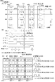
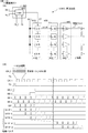
図4及び図5は、画素回路10と、当該画素回路10を備えた表示装置の一形態を示す図である。図4は基本構成(1画素分)を示し、図5は具体的な構成(表示装置の全体)を示す。尚、表示パネル部100の基板101上において画素回路10の周辺部に設けられた垂直駆動部103と水平駆動部106も合わせて示している。
[Pixel circuit]
4 and 5 are diagrams illustrating one mode of the
表示装置1は、映像信号Vsig(詳しくは信号振幅ΔVin)に基づいて画素回路10内の電気光学素子(本例では発光部ELPとして有機EL素子127を使用する)を発光させる。このため、表示装置1は、画素アレイ部102に行列状に配される画素回路10内に、少なくとも、駆動電流を生成する駆動トランジスタ121(駆動トランジスタTRD)、駆動トランジスタ121の制御入力端(ゲート端が典型例)と出力端(ソース端が典型例)の間に接続された保持容量120(保持容量Ccs)、駆動トランジスタ121の出力端に接続された電気光学素子の一例である有機EL素子127(発光部ELP)、及び、保持容量120に信号振幅ΔVinに応じた情報を書き込むサンプリングトランジスタ125(書込トランジスタTRW)を備える。この画素回路10においては、保持容量120に保持された情報に基づく駆動電流Idsを駆動トランジスタ121で生成して電気光学素子の一例である有機EL素子127に流すことで有機EL素子127を発光させる。
The
サンプリングトランジスタ125で保持容量120に信号振幅ΔVinに応じた情報を書き込むので、サンプリングトランジスタ125は、その入力端(ソース端もしくはドレイン端の一方)に信号電位(Vofs+ΔVin)を取り込み、その出力端(ソース端もしくはドレイン端の他方)に接続された保持容量120に信号振幅ΔVinに応じた情報を書き込む。もちろん、サンプリングトランジスタ125の出力端は、駆動トランジスタ121の制御入力端にも接続されている。
Since the
尚、ここで示した画素回路10の接続構成は、最も基本的な構成を示したもので、画素回路10は、少なくとも前述の各構成要素を含むものであればよく、これらの構成要素以外(つまり他の構成要素)が含まれていてもよい。又、「接続」は、直接に接続されている場合に限らず、他の構成要素を介在して接続されている場合でもよい。例えば、接続間には、必要に応じて更に、スイッチング用のトランジスタや、ある機能を持った機能部等を介在させる等の変更が加えられることがある。典型的には、表示期間(換言すれば非発光時間)を動的に制御するためにスイッチング用のトランジスタを、駆動トランジスタ121の出力端と電気光学素子(有機EL素子127)と間に、もしくは駆動トランジスタ121の電源供給端(ドレイン端が典型例)と電源供給用の配線である電源線PWL(本例では電源供給線105DSL)との間に配することがある。このような変形態様の画素回路であっても、実施例1(或いはその他の実施例)で説明する構成や作用を実現し得るものである限り、それらの変形態様も、本開示に係る表示装置の一実施形態を実現する画素回路10である。
Note that the connection configuration of the
又、画素回路10を駆動するための周辺部には、例えば、サンプリングトランジスタ125を水平周期で順次制御することで画素回路10を線順次走査して、1行分の各保持容量120に映像信号Vsigの信号振幅ΔVinに応じた情報を書き込む書込走査部104、及び、書込走査部104での線順次走査に合わせて1行分の各駆動トランジスタ121の電源供給端に印加される電源供給を制御するための走査駆動パルス(電源駆動パルスDSL)を出力する駆動走査部105を具備する制御部109を設ける。又、制御部109には、書込走査部104での線順次走査に合わせて各水平周期内で基準電位(Vofs)と信号電位(Vofs+ΔVin)で切り替わる映像信号Vsigがサンプリングトランジスタ125に供給されるように制御する水平駆動部106を設ける。
Further, in the peripheral portion for driving the
制御部109は、好ましくは、保持容量120に信号振幅ΔVinに対応する情報が書き込まれた時点でサンプリングトランジスタ125を非導通状態にして駆動トランジスタ121の制御入力端への映像信号Vsigの供給を停止させ、駆動トランジスタ121の出力端の電位変動に制御入力端の電位が連動するブートストラップ動作を行なうように制御するのがよい。制御部109は、好ましくは、ブートストラップ動作を、サンプリング動作の終了後の発光開始の初期でも実行するようにする。即ち、信号電位(Vofs+ΔVin)がサンプリングトランジスタ125に供給されている状態でサンプリングトランジスタ125を導通状態にした後にサンプリングトランジスタ125を非導通状態にすることで、駆動トランジスタ121の制御入力端と出力端の電位差が一定に維持されるようにする。
The
又、制御部109は、好ましくはブートストラップ動作を、発光期間において電気光学素子(有機EL素子127)の経時変動補正動作を実現するように制御する。このため、制御部109は、保持容量120に保持された情報に基づく駆動電流Idsが電気光学素子(有機EL素子127)に流れている期間は継続的にサンプリングトランジスタ125を非導通状態にしておくことで、制御入力端と出力端の電圧を一定に維持可能にして電気光学素子の経時変動補正動作を実現するとよい。発光時における保持容量120のブートストラップ動作により有機EL素子127の電流−電圧特性が経時変動しても駆動トランジスタ121の制御入力端と出力端の電位差をブートストラップした保持容量120により一定に保つことで、常に一定の発光輝度を保つようにする。又、好ましくは、制御部109は、基準電位(=第1ノード初期化電圧Vofs)がサンプリングトランジスタ125の入力端(ソース端が典型例)に供給されている時間帯でサンプリングトランジスタ125を導通させることで駆動トランジスタ121の閾値電圧Vthに対応する電圧を保持容量120に保持するための閾値補正動作を行なうように制御する。
Further, the
この閾値補正動作は、必要に応じて、信号振幅ΔVinに対応する情報の保持容量120への書込みに先行する複数の水平周期で繰り返し実行するとよい。ここで「必要に応じて」とは、1水平周期内の閾値補正期間では駆動トランジスタ121の閾値電圧に相当する電圧を十分に保持容量120へ保持させることができない場合を意味する。閾値補正動作の複数回の実行により、確実に駆動トランジスタ121の閾値電圧Vthに相当する電圧を保持容量120に保持させる。閾値補正を複数回行なう処理を分割閾値補正とも称する。
This threshold value correcting operation may be repeatedly executed at a plurality of horizontal periods preceding the writing of information corresponding to the signal amplitude ΔV in to the
又、更に好ましくは、制御部109は、閾値補正動作に先立って、サンプリングトランジスタ125の入力端に基準電位(Vofs)が供給されている時間帯でサンプリングトランジスタ125を導通させて閾値補正用の準備動作(放電動作や初期化動作)を実行するように制御する。閾値補正動作前に駆動トランジスタ121の制御入力端と出力端の電位を初期化しておく。より詳しくは、制御入力端と出力端と間に保持容量120を接続しておくことで、保持容量120の両端の電位差が閾値電圧Vth以上になるように設定する。
More preferably, prior to the threshold value correcting operation, the
尚、2Tr/1C駆動構成における閾値補正に当たっては、制御部109には、書込走査部104での線順次走査に合わせて1行分の各画素回路10に、駆動電流Idsを電気光学素子(有機EL素子127)に流すために使用される第1電位Vcc_Hと第1電位Vcc_Hとは異なる第2電位Vcc_Lとを切り替えて出力する駆動走査部105を設け、駆動トランジスタ121の電源供給端子に第1電位Vcc_Hに対応する電圧が供給され、かつサンプリングトランジスタ121に信号電位(Vofs+ΔVin)が供給されている時間帯でサンプリングトランジスタ125を導通させることで閾値補正動作を行なうように制御するのがよい。又、2TR駆動構成における閾値補正の準備動作に当たっては、駆動トランジスタ121の電源供給端に第2電位Vcc_L(=第2ノード初期化電圧Vini)に対応する電圧が供給され、かつサンプリングトランジスタ125に基準電位(Vofs)が供給されている時間帯でサンプリングトランジスタ125を導通させて、駆動トランジスタ121の制御入力端(つまり第1ノードND1)の電位を基準電位(Vofs)に、又出力端(つまり第2ノードND2)の電位を第2電位Vcc_Lに初期化するのがよい。
In the threshold correction in the 2Tr / 1C driving configuration, the
更に好ましくは、制御部109は、閾値補正動作の後、駆動トランジスタ121に第1電位Vcc_Hに対応する電圧が供給され、サンプリングトランジスタ125に信号電位(Vofs+ΔVin)が供給されている時間帯でサンプリングトランジスタ125を導通させることで保持容量120に信号振幅ΔVinの情報を書き込む際、駆動トランジスタ121の移動度μに対する補正分を保持容量120に書き込まれる情報に加えるように制御する。この際には、サンプリングトランジスタ125に信号電位(Vofs+ΔVin)が供給されている時間帯内の所定位置で、その時間帯より短い期間だけサンプリングトランジスタ125を導通させるとよい。以下2Tr/1C駆動構成での画素回路10の一例について具体的に説明する。
More preferably, after the threshold correction operation, the
画素回路10は、基本的にnチャネル型の薄膜電界効果トランジスタで駆動トランジスタが構成されている。又、有機EL素子の経時劣化による当該有機EL素子への駆動電流Idsの変動を抑制するための回路、即ち電気光学素子の一例である有機EL素子の電流−電圧特性の変化を補正して駆動電流Idsを一定に維持する駆動信号一定化回路(その1)を備え、又駆動トランジスタの特性変動(閾値電圧ばらつきや移動度ばらつき)による駆動電流変動を防ぐ閾値補正機能や移動度補正機能を実現して駆動電流Idsを一定に維持する駆動方式を採用した点に特徴を有する。
The
駆動トランジスタ121の特性変動(例えば閾値電圧や移動度等のばらつきや変動)による駆動電流Idsに与える影響を抑制する方法としては、2TR構成の駆動回路をそのまま駆動信号一定化回路(その1)として採用しつつ、各トランジスタ(駆動トランジスタ121及びサンプリングトランジスタ125)の駆動タイミングを工夫することで対処する。画素回路10は、2TR駆動の構成であり、素子数や配線数が少ないため、高精細化が可能であることに加えて、映像信号Vsigの劣化なくサンプリングできるため、良好な画質を得ることができる。
As a method of suppressing the influence on the drive current I ds due to the characteristic variation of the drive transistor 121 (for example, variation or fluctuation in threshold voltage, mobility, etc.), the drive circuit of the 2TR configuration is used as it is as a drive signal stabilization circuit (part 1). This is dealt with by devising the drive timing of each transistor (
又、画素回路10は、保持容量120の接続態様に特徴を有し、有機EL素子127の経時劣化による駆動電流変動を防ぐ回路として、駆動信号一定化回路(その2)の一例であるブートストラップ回路を構成している。有機EL素子の電流−電圧特性に経時変化があった場合でも駆動電流を一定にする(駆動電流変動を防ぐ)ブートストラップ機能を実現する駆動信号一定化回路(その2)を備えた点に特徴を有する。
The
駆動トランジスタを始めとする各トランジスタとしてはFET(電界効果トランジスタ)を使用する。この場合、駆動トランジスタについては、ゲート端を制御入力端として取り扱い、ソース端及びドレイン端の何れか一方(ここではソース端とする)を出力端として取り扱い、他方を電源供給端(ここではドレイン端とする)として取り扱う。 FETs (field effect transistors) are used as the transistors including the driving transistor. In this case, for the drive transistor, the gate end is handled as a control input end, either the source end or the drain end (here, the source end) is handled as the output end, and the other is the power supply end (here the drain end). ).
具体的には図4及び図5に示すように、画素回路10は、それぞれnチャネル型の駆動トランジスタ121及びサンプリングトランジスタ125と、電流が流れることで発光する電気光学素子の一例である有機EL素子127とを有する。一般に、有機EL素子127は整流性があるためダイオードの記号で表している。尚、有機EL素子127には、寄生容量Celが存在する。図では、この寄生容量Celを有機EL素子127(ダイオード状のもの)と並列に示す。
Specifically, as illustrated in FIGS. 4 and 5, the
駆動トランジスタ121は、ドレイン端Dが第1電位Vcc_H或いは第2電位Vcc_Lを供給する電源供給線105DSLに接続され、ソース端Sが、有機EL素子127のアノード端Aに接続され(その接続点は第2ノードND2でありノードND122とする)、有機EL素子127のカソード端Kが基準電位を供給する全画素回路10共通のカソード配線cath(電位はカソード電位Vcath、例えばGND)に接続されている。尚、カソード配線cathは、それ用の単一層の配線(上層配線)のみとしてもよいし、例えばアノード用の配線が形成されるアノード層に、カソード配線用の補助配線を設けてカソード配線の抵抗値を低減するようにしてもよい。この補助配線は、画素アレイ部102(表示エリア)内に格子状又は列又は行状に配線され、上層配線と同電位で固定電位である。
The
サンプリングトランジスタ125は、ゲート端Gが書込走査部104からの書込走査線104WSに接続され、ドレイン端Dが映像信号線106HS(映像信号線DTL)に接続され、ソース端Sが駆動トランジスタ121のゲート端Gに接続されている(その接続点は第1ノードND1でありノードND121とする)。サンプリングトランジスタ125のゲート端Gには、書込走査部104からアクティブHの書込駆動パルスWSが供給される。サンプリングトランジスタ125は、ソース端Sとドレイン端Dとを逆転させた接続態様とすることもできる。
The
駆動トランジスタ121のドレイン端Dは、電源スキャナとして機能する駆動走査部105からの電源供給線105DSLに接続されている。電源供給線105DSLは、この電源供給線105DSLそのものが、駆動トランジスタ121に対しての電源供給能力を備える点に特徴を有する。駆動走査部105は、駆動トランジスタ121のドレイン端Dに対して、それぞれ電源電圧に相当する高電圧側の第1電位Vcc_Hと閾値補正に先立つ準備動作に利用される低電圧側の第2電位Vcc_L(初期化電圧もしくはイニシャル電圧とも称される)とを切り替えて供給する。
The drain terminal D of the
駆動トランジスタ121のドレイン端D側(電源回路側)を第1電位Vcc_Hと第2電位Vcc_Lの2値をとる電源駆動パルスDSLで駆動することで、閾値補正に先立つ準備動作を行なうことを可能にしている。第2電位Vcc_Lとしては、映像信号線106HSにおける映像信号Vsigの基準電位(Vofs)より十分低い電位とする。具体的には、駆動トランジスタ121のゲート・ソース間電圧Vgs(ゲート電位Vgとソース電位Vsの差)が駆動トランジスタ121の閾値電圧Vthより大きくなるように、電源供給線105DSLの低電位側の第2電位Vcc_Lを設定する。尚、基準電位(Vofs)は、閾値補正動作に先立つ初期化動作に利用するとともに映像信号線106HSを予めプリチャージにしておくためにも利用する。
By driving the drain end D side (power supply circuit side) of the
このような画素回路10では、有機EL素子127を駆動するときには、駆動トランジスタ121のドレイン端Dに第1電位Vcc_Hが供給され、ソース端Sが有機EL素子127のアノード端A側に接続されることで、全体としてソースフォロワ回路を形成するようになっている。
In such a
このような画素回路10を採用する場合、駆動トランジスタ121の他に走査用に1つのスイッチングトランジスタ(サンプリングトランジスタ125)を使用する2TR駆動の構成を採るとともに、各スイッチングトランジスタを制御する電源駆動パルスDSL及び書込駆動パルスWSのオン/オフタイミングの設定により、有機EL素子127の経時劣化や駆動トランジスタ121の特性変動(例えば閾値電圧や移動度等のばらつきや変動)による駆動電流Idsに与える影響を防ぐ。
When such a
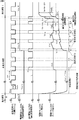
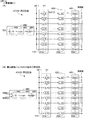
[画素回路の動作]
図6は、画素回路10に関する駆動タイミングの一例として、線順次方式で信号振幅Vinの情報を保持容量120に書き込む際の動作を説明するタイミングチャート(理想状態)である。図7は、図6に示したタイミングチャートの主要な期間における等価回路と動作状態を説明する図である。図6においては、時間軸を共通にして、書込走査線104WSの電位変化、電源供給線105DSLの電位変化、映像信号線106HSの電位変化を表してある。これらの電位変化と並行に、駆動トランジスタ121のゲート電位Vg及びソース電位Vsの変化も表してある。基本的には、書込走査線104WSや電源供給線105DSLの1行ごとに、1水平走査期間だけ遅れて同じような駆動を行なう。
[Operation of pixel circuit]
Figure 6 is an example of a driving timing regarding the
図6中の信号のように各パルスのタイミングによって有機EL素子127に流れる電流値をコントロールする。図6のタイミング例では、電源駆動パルスDSLを第2電位Vcc_Lとすることで消光及びノードND122を初期化した後に、第1ノード初期化電圧Vofsを映像信号線106HSに印加している際にサンプリングトランジスタ125をオン状態としてノードND121を初期化し、その状態で電源駆動パルスDSLを第1電位Vcc_Hとすることで閾値補正を行なう。その後、サンプリングトランジスタ125をオフ状態とし、映像信号線106HSに映像信号Vsigを印加する。その状態でサンプリングトランジスタ125をオン状態とすることにより信号を書き込むと同時に移動度補正を行なう。信号を書き込んだ後、サンプリングトランジスタ125をオフ状態にすると発光を開始する。このように移動度補正や閾値補正等、パルスの位相差によって駆動をコントロールする。
The value of the current flowing through the
以下、閾値補正及び移動度補正に着目して動作を詳しく説明する。画素回路10において、駆動タイミングとしては、先ず、サンプリングトランジスタ125は、書込走査線104WSから供給された書込駆動パルスWSに応じて導通し、映像信号線106HSから供給された映像信号Vsigをサンプリングして保持容量120に保持する。最初に、以下では、説明や理解を容易にするため、特段の断りのない限り、書込みゲインが1(理想値)であると仮定して、保持容量120に信号振幅Vinの情報を、書き込む、保持する、あるいはサンプリングする等と簡潔に記して説明する。書込みゲインが1未満の場合、保持容量120には信号振幅Vinの大きさそのものではなく、信号振幅Vinの大きさに対応するゲイン倍された情報が保持されることになる。
Hereinafter, the operation will be described in detail focusing on threshold correction and mobility correction. In the
画素回路10に対する駆動タイミングは、映像信号Vsigの信号振幅Vinの情報を保持容量120に書き込む際に、順次走査の観点からは、1行分の映像信号を同時に各列の映像信号線106HSに伝達する線順次駆動を行なう。特に、2TR構成の画素回路10における駆動タイミングでの閾値補正と移動度補正を行なう際の基本的な考え方においては、先ず、映像信号Vsigを基準電位(Vofs)と信号電位(Vofs+Vin)とを1H期間内において時分割で有するものとする。具体的には、映像信号Vsigが非有効期間である基準電位(Vofs)にある期間を1水平期間の前半部とし、有効期間である信号電位(Vsig=Vofs+Vin)にある期間を1水平期間の後半部とする。1水平期間を前半部と後半部に分ける際は、典型的にはほぼ1/2期間ずつ分けるがこのことは必須でなく、前半部よりも後半部の方をより長くしてもよいし、逆に、前半部よりも後半部の方をより短くしてもよい。
The drive timing for the
信号書込みに用いる書込駆動パルスWSを閾値補正や移動度補正にも用いることとし、1H期間内に2回、書込駆動パルスWSをアクティブにしてサンプリングトランジスタ125をオンする。そして、1回目のオンタイミングにて閾値補正を行ない、2回目のオンタイミングにて信号電圧書込みと移動度補正を同時に行なう。その後、駆動トランジスタ121は、第1電位(高電位側)にある電源供給線105DSLから電流の供給を受け保持容量120に保持された信号電位(映像信号Vsigの有効期間の電位に対応する電位)に応じて駆動電流Idsを有機EL素子127に流す。尚、1H期間内に2回、書込駆動パルスWSをアクティブにするのではなく、サンプリングトランジスタ125のオン状態を維持したまま、映像信号線106HSの電位を、有機EL素子127における輝度を制御するための信号電位(=Vofs+Vin)としてもよい。
The writing drive pulse WS used for signal writing is also used for threshold correction and mobility correction, and the
例えば、有機EL素子127の発光状態は、電源供給線105DSLが第1電位Vcc_Hであり、サンプリングトランジスタ125がオフ状態である(図6(A)を参照)。このとき、駆動トランジスタ121は飽和領域で動作するように設定されているため、有機EL素子127に流れる電流Idsは駆動トランジスタ121のゲート・ソース間電圧Vgs(ノードND121とノードND122との間の電圧)に応じて決まる式(1)に示される値となる。その後、垂直駆動部103は、電源供給線105DSLが第1電位Vcc_Hにありかつ映像信号線106HSが映像信号Vsigの非有効期間である基準電位(Vofs)にある時間帯でサンプリングトランジスタ125を導通させる制御信号として書込駆動パルスWSを出力して、駆動トランジスタ121の閾値電圧Vthに相当する電圧を保持容量120に保持しておく(図6(D)を参照)。この動作が閾値補正機能を実現する。この閾値補正機能により、画素回路10ごとにばらつく駆動トランジスタ121の閾値電圧Vthの影響をキャンセルすることができる。
For example, the light emission state of the
垂直駆動部103は、信号振幅Vinのサンプリングに先行する複数の水平期間で閾値補正動作を繰り返し実行して確実に駆動トランジスタ121の閾値電圧Vthに相当する電圧を保持容量120に保持するようにするのがよい。閾値補正動作を複数回実行することで、十分に長い書込み時間を確保する。こうすることで、駆動トランジスタ121の閾値電圧Vthに相当する電圧を確実に保持容量120に予め保持することができる。
The
保持された閾値電圧Vthに相当する電圧は駆動トランジスタ121の閾値電圧Vthのキャンセルに用いられる。したがって、画素回路10ごとに駆動トランジスタ121の閾値電圧Vthがばらついていても、画素回路10ごとに完全にキャンセルされるため、画像のユニフォーミティすなわち表示装置の画面全体に亘る発光輝度の均一性が高まる。特に信号電位が低階調のときに現れがちな輝度むらを防ぐことができる。
Voltage corresponding to the held threshold voltage V th is used to cancel the threshold voltage V th of the
好ましくは、垂直駆動部103は、閾値補正動作に先立って、電源供給線105DSLが第2電位にありかつ映像信号線106HSが映像信号Vsigの非有効期間である基準電位(Vofs)にある時間帯で、書込駆動パルスWSをアクティブ(本例ではHレベル)にしてサンプリングトランジスタ125を導通させ、その後に書込駆動パルスWSをアクティブHにしたままで電源供給線105DSLを第1電位に設定する。
Preferably, prior to the threshold correction operation, the
こうすることで、ソース端Sを基準電位(Vofs)より十分低い第2電位Vcc_Lにセットし(放電期間C=第2ノード初期化期間)(図6(B)を参照)、且つ、駆動トランジスタ121のゲート端Gを基準電位(Vofs)にセットしてから(初期化期間D=第1ノード初期化期間)(図6(C)を参照)、閾値補正動作を開始する(閾値補正期間E)。このようなゲート電位及びソース電位のリセット動作(初期化動作)により、後続する閾値補正動作を確実に実行することができる。放電期間Cと初期化期間Dとを合わせて、駆動トランジスタ121のゲート電位Vgとソース電位Vsを初期化する閾値補正準備期間(=前処理期間)とも称する。因みに、図示した例は、第1ノードのであるノードND121への初期化動作(初期化期間D)は3回繰り返しており、放電期間Cの開始から最後の初期化期間Dが完了するまでが閾値補正準備期間となる。
In this way, the source terminal S is set to the second potential V cc_L sufficiently lower than the reference potential (V ofs ) (discharge period C = second node initialization period) (see FIG. 6B), and After the gate terminal G of the driving
閾値補正期間Eでは、電源供給線105DSLの電位が低電位側の第2電位Vcc_Lから高電位側の第1電位Vcc_Hに遷移することで、駆動トランジスタ121のソース電位Vsが上昇を開始する。即ち、駆動トランジスタ121のゲート端Gは映像信号Vsigの基準電位(Vofs)に保持されており、駆動トランジスタ121のソース端Sの電位Vsが上昇して駆動トランジスタ121がカットオフするまでドレイン電流が流れようとする。カットオフすると駆動トランジスタ121のソース電位Vsは“Vofs−Vth”となる。閾値補正期間Eでは、ドレイン電流が専ら保持容量120側(Ccs<<Cel時)に流れ、有機EL素子127側には流れないようにするため、有機EL素子127がカットオフとなるように全画素共通の接地配線cathの電位Vcathを設定しておく。
In the threshold value correction period E, that the potential of the power supply line 105DSL transits from the second potential V cc - L on the low potential side to the first potential V cc - H on the high potential side, the source potential V s of the driving
有機EL素子127の等価回路はダイオードと寄生容量Celの並列回路で表されるため、“Vel≦Vcath+VthEL”である限り、つまり、有機EL素子127のリーク電流が駆動トランジスタ121に流れる電流よりもかなり小さい限り、駆動トランジスタ121のドレイン電流Idsは保持容量120と寄生容量Celを充電するために使われる。この結果、有機EL素子127のアノード端Aの電圧VelつまりノードND122の電位は、時間とともに上昇してゆく。そして、ノードND122の電位(ソース電位Vs)とノードND121の電圧(ゲート電位Vg)との電位差がちょうど閾値電圧Vthとなったところで駆動トランジスタ121はオン状態からオフ状態となり、ドレイン電流Idsは流れなくなり、閾値補正期間が終了する。つまり、一定時間経過後、駆動トランジスタ121のゲート・ソース間電圧Vgsは閾値電圧Vthという値をとる。
Since the equivalent circuit of the
ここで、閾値補正動作は1回のみ実行するものとすることもできるが、このことは必須ではない。1水平期間を処理サイクルとして、閾値補正動作を複数回(図は4回で示している)繰り返えしてもよい。例えば、実際には、閾値電圧Vthに相当する電圧が、駆動トランジスタ121のゲート端Gとソース端Sと間に接続された保持容量120に書き込まれることになる。しかしながら、閾値補正期間Eは、書込駆動パルスWSをアクティブHにしたタイミングからインアクティブLに戻すタイミングまでであり、この期間が十分に確保されていないときには、それ以前に終了してしまう。この問題を解消するには、閾値補正動作を複数回繰り返すのがよい。
Here, the threshold correction operation may be executed only once, but this is not essential. The threshold correction operation may be repeated a plurality of times (shown as four times in the figure) with one horizontal period as a processing cycle. For example, actually, a voltage corresponding to the threshold voltage V th is written in the
閾値補正動作を複数回実行する場合に、1水平期間が閾値補正動作の処理サイクルとなるのは、閾値補正動作に先立って、1水平期間の前半部で映像信号線106HSを介して基準電位(Vofs)を供給しソース電位を第2電位Vcc_Lにセットする初期化動作を経るからである。必然的に、閾値補正期間は、1水平期間よりも短くなってしまう。したがって、保持容量120の静電容量Ccsや第2電位Vcc_Lの大きさ関係やその他の要因で、この短い1回分の閾値補正動作期間では、閾値電圧Vthに対応する正確な電圧を保持容量120に保持仕切れないケースも起こり得る。閾値補正動作を複数回実行するのが好ましいのは、この対処のためである。即ち、信号振幅Vinの保持容量120へのサンプリング(信号書込み)に先行する複数の水平周期で、閾値補正動作を繰り返し実行することで確実に駆動トランジスタ121の閾値電圧Vthに相当する電圧を保持容量120に保持させるのが好ましい。
When the threshold correction operation is executed a plurality of times, the processing cycle of the threshold correction operation in one horizontal period is the reference potential (via the video signal line 106HS in the first half of the one horizontal period prior to the threshold correction operation. supply V ofs) because undergo an initialization operation for setting the source potential to the second potential V cc - L. Inevitably, the threshold correction period is shorter than one horizontal period. Accordingly, an accurate voltage corresponding to the threshold voltage Vth is held in this short one-time threshold correction operation period due to the magnitude relationship between the capacitance C cs of the holding
例えば、第1閾値補正期間E_1ではゲート・ソース間電圧VgsがVx1(>Vth)になったとき、つまり、駆動トランジスタ121のソース電位Vsが低電位側の第2電位Vcc_Lから“Vofs−Vx1”になったときに終わってしまう(図6(D)を参照)。このため、第1閾値補正期間E_1が完了した時点では、Vx1が保持容量120に書き込まれる。
For example, in the first threshold correction period E_1, when the gate-source voltage V gs becomes V x1 (> V th ), that is, the source potential V s of the
次に、駆動走査部105は、1水平期間の後半部で、書込駆動パルスWSをインアクティブLに切り替え、さらに水平駆動部106は、映像信号線106HSの電位を基準電位(Vofs)から映像信号Vsig(=Vofs+Vin)に切り替える(図6(E)を参照)。これにより、映像信号線106HSが映像信号Vsigの電位に変化する一方、書込走査線104WSの電位(書込駆動パルスWS)はローレベルになる。
Next, the driving
このときには、サンプリングトランジスタ125は非導通(オフ)状態にあり、それ以前に保持容量120に保持されたVx1に応じたドレイン電流が有機EL素子127に流れることで、ソース電位Vsが僅かに上昇する。この上昇分をVa1とすると、ソース電位Vsは“Vofs−Vx1+Va1”となる。さらに、駆動トランジスタ121のゲート端Gとソース端Sとの間には保持容量120が接続されており、その保持容量120による効果によって、駆動トランジスタ121のソース電位Vsの変動にゲート電位Vgが連動することで、ゲート電位Vgが“Vofs+Va1”となる。
At this time, the
次の第2閾値補正期間E_2では、第1閾値補正期間E_1と同様の動作をする。具体的には、先ず、駆動トランジスタ121のゲート端Gは映像信号Vsigの基準電位(Vofs)に保持されることとなり、ゲート電位Vgが直前の“Vg=基準電位(Vofs)+Va1”から基準電位(Vofs)に瞬時に切り替わる。駆動トランジスタ121のゲート端Gとソース端Sとの間には保持容量120が接続されており、その保持容量120による効果によって、駆動トランジスタ121のゲート電位Vgの変動にソース電位Vsが連動することで、ソース電位Vsは、直前の“Vofs−Vx1+Va1”からVa1だけ低下するので、“Vofs−Vx1”となる。この後、駆動トランジスタ121のソース端Sの電位Vsが上昇して駆動トランジスタ121がカットオフするまでドレイン電流が流れようとする。しかしながら、ゲート・ソース間電圧VgsがVx2(>Vth)になったとき、つまり、駆動トランジスタ121のソース電位Vsが“Vofs−Vx2”になったときに終わってしまい、第2閾値補正期間E_2が完了した時点ではVx2が保持容量120に書き込まれる。次の第3閾値補正期間E_3の直前では、保持容量120に保持されたVx2に応じたドレイン電流が有機EL素子127に流れることで、ソース電位Vsは“Vofs−Vx2+Va2”となり、ゲート電位Vgは“Vofs+Va2”となる。
In the next second threshold correction period E_2, the same operation as in the first threshold correction period E_1 is performed. Specifically, first, the gate terminal G of the driving
同様にして、次の第3閾値補正期間E_3では、ゲート・ソース間電圧VgsがVx3(>Vth)になったとき、つまり、駆動トランジスタ121のソース電位Vsが“Vofs−Vx3”になったときに終わってしまい、第3閾値補正期間E_3が完了した時点ではVx3が保持容量120に書き込まれる。次の第4閾値補正期間E_4の直前では、保持容量120に保持されたVx3に応じたドレイン電流が有機EL素子127に流れることで、ソース電位Vsは“Vofs−Vx3+Va3”となり、ゲート電位Vgは“Vofs+Va3”となる。
Similarly, in the next third threshold value correction period E_3, when the gate-source voltage V gs becomes V x3 (> V th ), that is, the source potential V s of the
そして、次の第4閾値補正期間E_4では、駆動トランジスタ121のソース端Sの電位Vsが上昇して駆動トランジスタ121がカットオフするまでドレイン電流が流れる。カットオフすると駆動トランジスタ121のソース電位Vsは“Vofs−Vth”となり、ゲート・ソース間電圧Vgsが閾値電圧Vthと同じ状態になっている。第4閾値補正期間E_4が完了した時点で、駆動トランジスタ121の閾値電圧Vthが保持容量120に保持される。
Then, in the next fourth threshold value correction period E_4, the potential V s of the source terminal S rises driving
画素回路10においては、閾値補正機能に加えて、移動度補正機能を備えている。即ち、垂直駆動部103は、映像信号線106HSが映像信号Vsigの有効期間である信号電位(Vofs+Vin)にある時間帯にサンプリングトランジスタ125を導通状態にするため、書込走査線104WSに供給する書込駆動パルスWSを、上述の時間帯より短い期間だけアクティブ(本例ではHレベル)にする。この期間では、駆動トランジスタ121の制御入力端に信号電位(Vofs+Vin)を供給した状態で駆動トランジスタ121を介して有機EL素子127の寄生容量Cel及び保持容量120を充電する(図6(F)を参照)。この書込駆動パルスWSのアクティブ期間(サンプリング期間でもあり移動度補正期間でもある)を適切に設定することで、保持容量120に信号振幅Vinに応じた情報を保持する際、同時に駆動トランジスタ121の移動度μに対する補正を加えることができる。水平駆動部106により映像信号線106HSに信号電位(Vofs+Vin)を実際に供給して、書込駆動パルスWSをアクティブHにする期間を、保持容量120への信号振幅Vinの書込み期間(サンプリング期間とも称する)とする。
The
特に、画素回路10における駆動タイミングでは、電源供給線105DSLが高電位側である第1電位Vcc_Hにあり、かつ、映像信号Vsigが有効期間にある時間帯内(信号振幅Vinの期間)で書込駆動パルスWSをアクティブにしている。つまり、その結果、移動度補正時間(サンプリング期間も)は、映像信号線106HSの電位が、映像信号Vsigの有効期間の信号電位(Vofs+Vin)にある時間幅と書込駆動パルスWSのアクティブ期間の両者が重なった範囲で決まる。特に、映像信号線106HSが信号電位にある時間幅の中に入るように書込駆動パルスWSのアクティブ期間幅を細めに決めているため、結果的に移動度補正時間は書込駆動パルスWSで決まる。正確には、移動度補正時間(サンプリング期間も)は、書込駆動パルスWS立ち上がってサンプリングトランジスタ125がオンしてから、同じく書込駆動パルスWSが立ち下がってサンプリングトランジスタ125がオフするまでの時間となる。因みに、図では、第4閾値補正期間E_4の後で書込駆動パルスWSを一端インアクティブLにしているが、このことは必須でなく、アクティブHのままにして、映像信号Vsigを基準電位(Vofs)から有効期間の信号電位(Vofs+Vin)に切り替えてもよい。
In particular, in the driving timing in the
具体的には、サンプリング期間においては、駆動トランジスタ121のゲート電位Vgが信号電位(Vofs+Vin)にある状態でサンプリングトランジスタ125が導通(オン)状態となる。したがって、書込み&移動度補正期間Hでは、駆動トランジスタ121のゲート端Gが信号電位(Vofs+Vin)に固定された状態で、駆動トランジスタ121に駆動電流Idsが流れる。信号振幅Vinの情報は駆動トランジスタ121の閾値電圧Vthに足し込む形で保持される。この結果、駆動トランジスタ121の閾値電圧Vthの変動は常にキャンセルされる形となるので、閾値補正を行なっていることになる。この閾値補正によって、保持容量120に保持されるゲート・ソース間電圧Vgsは、“Vsig+Vth”=“Vin+Vth”となる。又、同時に、このサンプリング期間で移動度補正を実行するので、サンプリング期間は移動度補正期間を兼ねることとなる(書込み&移動度補正期間H)。
Specifically, in the sampling period, the
ここで、有機EL素子127の閾値電圧をVthELとしたとき、“Vofs−Vth<VthEL”と設定しておくことで、有機EL素子127は、逆バイアス状態におかれ、カットオフ状態(ハイインピーダンス状態)にあるため、発光することはなく、又、ダイオード特性ではなく単純な容量特性を示す。よって駆動トランジスタ121に流れるドレイン電流(駆動電流Ids)は保持容量120の静電容量Ccsと有機EL素子127の寄生容量(等価容量)Celの静電容量Celの両者を結合した容量“C=Ccs+Cel”に書き込まれていく。これにより、駆動トランジスタ121のドレイン電流は有機EL素子127の寄生容量Celに流れ込み充電を開始する。その結果、駆動トランジスタ121のソース電位Vsは上昇していく。
Here, when the threshold voltage of the
図6のタイミングチャートでは、この上昇分をΔVで表してある。この上昇分、即ち移動度補正パラメータである電位補正値ΔVは、閾値補正によって保持容量120に保持されるゲート・ソース間電圧“Vgs=Vin+Vth”から差し引かれることになり、“Vgs=Vin+Vth−ΔV”となるので、負帰還をかけたことになる。このとき、駆動トランジスタ121のソース電位Vsは、ゲート電位Vg(=Vin)から保持容量に保持される電圧“Vgs=Vin+Vth−ΔV”を差し引いた値“−Vth+ΔV”となる。
In the timing chart of FIG. 6, this increase is represented by ΔV. This increase, that is, the potential correction value ΔV, which is a mobility correction parameter, is subtracted from the gate-source voltage “V gs = V in + V th ” held in the holding
このようにして、画素回路10における駆動タイミングでは、書込み&移動度補正期間Hにおいて、信号振幅Vinのサンプリングと移動度μを補正するΔV(負帰還量、移動度補正パラメータ)の調整が行なわれる。書込走査部104は、書込み&移動度補正期間Hの時間幅を調整可能であり、これにより保持容量120に対する駆動電流Idsの負帰還量を最適化することができる。
In this manner, in the driving timing in the
電位補正値ΔVはΔV≒Ids・t/Celである。この式から明らかなように、駆動トランジスタ121のドレイン・ソース間電流である駆動電流Idsが大きい程、電位補正値ΔVは大きくなる。逆に、駆動トランジスタ121の駆動電流Idsが小さいとき、電位補正値ΔVは小さくなる。このように、電位補正値ΔVは駆動電流Idsに応じて決まる。信号振幅Vinが大きいほど駆動電流Idsは大きくなり、電位補正値ΔVの絶対値も大きくなる。したがって、発光輝度レベルに応じた移動度補正を実現できる。その際、書込み&移動度補正期間Hは必ずしも一定である必要はなく、逆に駆動電流Idsに応じて調整することが好ましい場合がある。例えば、駆動電流Idsが大きい場合、移動度補正期間tは短めにし、逆に駆動電流Idsが小さくなると、書込み&移動度補正期間Hは長めに設定するのがよい。
The potential correction value ΔV is ΔV≈I ds · t / C el . As is clear from this equation, the potential correction value ΔV increases as the drive current I ds that is the drain-source current of the
又、電位補正値ΔVは、Ids・t/Celであり、画素回路10ごとに移動度μのばらつきに起因して駆動電流Idsがばらつく場合でも、それぞれに応じた電位補正値ΔVとなるので、画素回路10ごとの移動度μのばらつきを補正することができる。つまり、信号振幅Vinを一定とした場合、駆動トランジスタ121の移動度μが大きいほど電位補正値ΔVの絶対値が大きくなる。換言すると、移動度μが大きいほど電位補正値ΔVが大きくなるので、画素回路10ごとの移動度μのばらつきを取り除くことができる。
The potential correction value ΔV is I ds · t / C el , and even when the drive current I ds varies due to the variation in the mobility μ for each
画素回路10はブートストラップ機能も備えている。即ち、書込走査部104は、保持容量120に信号振幅Vinの情報が保持された段階で書込走査線104WSに対する書込駆動パルスWSの印加を解除し(即ちインアクティブL(ロー)にして)、サンプリングトランジスタ125を非導通状態にして駆動トランジスタ121のゲート端Gを映像信号線106HSから電気的に切り離す(発光期間I:図6(G)を参照)。発光期間Iに進むと、水平駆動部106は、その後の適当な時点で映像信号線106HSの電位を基準電位(Vofs)に戻す。
The
有機EL素子127の発光状態を第(m+m’−1)番目の水平走査期間まで継続する。以上によって、第(n,m)番目の副画素を構成する有機EL素子127の発光の動作が完了する。この後、次のフレーム(もしくはフィールド)に移って、再び、閾値補正準備動作、閾値補正動作、移動度補正動作、及び発光動作が繰り返される。
The light emitting state of the
発光期間Iでは、駆動トランジスタ121のゲート端Gは映像信号線106HSから切り離される。駆動トランジスタ121のゲート端Gへの信号電位(Vofs+Vin)の印加が解除されるので、駆動トランジスタ121のゲート電位Vgは上昇可能となる。駆動トランジスタ121のゲート端Gとソース端Sと間には保持容量120が接続されており、その保持容量120による効果によって、ブートストラップ動作が行なわれる。ブートストラップゲインが1(理想値)であると仮定した場合、駆動トランジスタ121のソース電位Vsの変動にゲート電位Vgが連動するようになり、ゲート・ソース間電圧Vgsを一定に維持することができる。このとき、駆動トランジスタ121に流れる駆動電流Idsは有機EL素子127に流れ、有機EL素子127のアノード電位は駆動電流Idsに応じて上昇する。この上昇分をVelとする。やがて、ソース電位Vsの上昇に伴い、有機EL素子127の逆バイアス状態は解消されるので、駆動電流Idsの流入により有機EL素子127は実際に発光を開始する。
In the light emission period I, the gate terminal G of the
ここで、駆動電流Ids対ゲート電圧Vgsの関係は、先のトランジスタ特性を表した式(1)に“Vsig+Vth−ΔV”或いは“Vin+Vth−ΔV”を代入することで、式(5A)或いは式(5B)(両式を纏めて式(5)と記す)のように表すことができる。 Here, the relationship between the drive current I ds and the gate voltage V gs is obtained by substituting “V sig + V th −ΔV” or “V in + V th −ΔV” into the equation (1) representing the transistor characteristics. , Expression (5A) or Expression (5B) (both expressions are collectively expressed as Expression (5)).
Ids=k・μ・(Vsig−Vofs−ΔV)2 (5A)
Ids=k・μ・(Vin−Vofs−ΔV)2 (5B)
I ds = k · μ · (V sig −V ofs −ΔV) 2 (5A)
I ds = k · μ · (V in −V ofs −ΔV) 2 (5B)
この式(5)から、閾値電圧Vthの項がキャンセルされており、有機EL素子127に供給される駆動電流Idsは駆動トランジスタ121の閾値電圧Vthに依存しないことが分かる。即ち、有機EL素子127を流れる電流Idsは、例えば、Vofsを0ボルトに設定したとした場合、有機EL素子127における輝度を制御するための映像信号Vsigの値から、駆動トランジスタ121の移動度μに起因した第2ノードND2(駆動トランジスタ121のソース端)における電位補正値ΔVの値を減じた値の2乗に比例する。換言すると、有機EL素子127を流れる電流Idsは、有機EL素子127の閾値電圧VthEL及び駆動トランジスタ121の閾値電圧Vthには依存しない。即ち、有機EL素子127の発光量(輝度)は、有機EL素子127の閾値電圧VthELの影響及び駆動トランジスタ121の閾値電圧Vthの影響を受けない。そして、第(n,m)番目の有機EL素子127の輝度は、電流Idsに対応した値である。
From this equation (5), it can be seen that the term of the threshold voltage V th is canceled and the drive current I ds supplied to the
しかも、移動度μの大きな駆動トランジスタ121ほど、電位補正値ΔVが大きくなるので、ゲート・ソース間電圧Vgsの値が小さくなる。したがって、式(5)において、移動度μの値が大きくとも、(Vsig−Vofs−ΔV)2の値が小さくなる結果、ドレイン電流Idsを補正することができる。即ち、移動度μの異なる駆動トランジスタ121においても、映像信号Vsigの値が同じであれば、ドレイン電流Idsが略同じとなる結果、有機EL素子127を流れ、有機EL素子127の輝度を制御する電流Idsが均一化される。即ち、移動度μのばらつき(更には、kのばらつき)に起因する有機EL素子127の輝度のばらつきを補正することができる。
Moreover, since the potential correction value ΔV increases as the driving
又、駆動トランジスタ121のゲート端Gとソース端Sと間には保持容量120が接続されており、その保持容量120による効果により、発光期間の最初でブートストラップ動作が行なわれ、駆動トランジスタ121のゲート・ソース間電圧“Vgs=Vin+Vth−ΔV”を一定に維持したまま、駆動トランジスタ121のゲート電位Vg及びソース電位Vsが上昇する。駆動トランジスタ121のソース電位Vsが“−Vth+ΔV+Vel”となることで、ゲート電位Vgは“Vin+Vel”となる。このとき、駆動トランジスタ121のゲート・ソース間電圧Vgsは一定であるので、駆動トランジスタ121は、一定電流(駆動電流Ids)を有機EL素子127に流す。その結果、有機EL素子127のアノード端Aの電位(=ノードND122の電位)は、有機EL素子127に飽和状態での駆動電流Idsという電流が流れ得る電圧まで上昇する。
In addition, a
ここで、有機EL素子127は、発光時間が長くなるとそのI−V特性が変化してしまう。そのため、時間の経過とともに、ノードND122の電位も変化する。しかしながら、このような有機EL素子127の経時劣化によりそのアノード電位が変動しても、保持容量120に保持されたゲート・ソース間電圧Vgsは常に“Vin+Vth−ΔV”で一定に維持される。駆動トランジスタ121が定電流源として動作することから、有機EL素子127のI−V特性が経時変化し、これに伴って駆動トランジスタ121のソース電位Vsが変化したとしても、保持容量120によって駆動トランジスタ121のゲート・ソース間電位Vgsが一定(≒Vin+Vth−ΔV)に保たれているため、有機EL素子127に流れる電流は変わらず、したがって有機EL素子127の発光輝度も一定に保たれる。実際にはブートストラップゲインは「1」よりも小さいので、ゲート・ソース間電位Vgsは「Vin+Vth−ΔV」よりも小さくなるが、そのブートストラップゲインに応じたゲート・ソース間電位Vgsに保たれることには変わりがない。
Here, the
以上のように、実施例1の画素回路10は、駆動タイミングを工夫することで、閾値補正回路や移動度補正回路が自動的に構成され、駆動トランジスタ121の特性ばらつき(本例では閾値電圧Vth及びキャリア移動度μのばらつき)による駆動電流Idsに与える影響を防ぐために、閾値電圧Vth及びキャリア移動度μによる影響を補正して駆動電流を一定に維持する駆動信号一定化回路として機能するようになっている。ブートストラップ動作だけでなく、閾値補正動作と移動度補正動作とを実行しているため、ブートストラップ動作で維持されるゲート・ソース間電圧Vgsは、閾値電圧Vthに相当する電圧と移動度補正用の電位補正値ΔVとによって調整されているため、有機EL素子127の発光輝度は駆動トランジスタ121の閾値電圧Vthや移動度μのばらつきの影響を受けることがないし、有機EL素子127の経時劣化の影響も受けない。入力される映像信号Vsig(信号振幅Vin)に対応する安定した階調で表示でき、高画質の画像を得ることができる。
As described above, in the
又、画素回路10は、nチャネル型の駆動トランジスタ121を用いたソースフォロア回路によって構成することができるために、現状のアノード・カソード電極の有機EL素子をそのまま用いても、有機EL素子127の駆動が可能になる。又、駆動トランジスタ121及びその周辺部のサンプリングトランジスタ125等も含めてnチャネル型のみのトランジスタを用いて画素回路10を構成することができ、トランジスタ作製においても低コスト化が図れる。
Further, since the
[表示むら現象の発生原因]
前述のように、図6に示した駆動タイミングでは、素子の特性むら(前例では駆動トランジスタ121の閾値電圧Vthや移動度μのばらつき及び経時変動)に起因する表示むらを改善するべく、書込駆動パルスWSや電源駆動パルスDSLのタイミングによって各トランジスタを制御して表示輝度を制御している。このため、駆動パルスの形状(振幅、レベル、幅等)がばらつくと、適正な制御ができなくなり、表示むらの原因となってしまう。
[Cause of display unevenness]
As described above, at the drive timing shown in FIG. 6, in order to improve display unevenness due to device characteristic unevenness (in the previous example, variation in threshold voltage V th and mobility μ of the
例えば、移動度補正においては、図6のタイミングチャートに示すように、信号書き込みを行ないながら移動度補正を行なう駆動となっており、移動度補正動作は、書込み&移動度補正期間Hを規定する書込駆動パルスWSのパルス幅に敏感に影響を受け、パルス幅の列ごとのばらつきがユニフォミティ劣化に直結する。又、移動度の大きなトランジスタ等の場合、閾値補正を複数回行なう分割閾値補正にあっては、休止期間中におけるブートストラップが顕著になる。特に、1回目の閾値補正のパルス形状が行ごとにばらつくとブートストラップの影響で補正に行ごとのばらつきが発生しユニフォミティが損なわれる。以下に、この点について説明する。 For example, in the mobility correction, as shown in the timing chart of FIG. 6, the mobility correction is performed while signal writing is performed, and the mobility correction operation defines the writing & mobility correction period H. Sensitively influenced by the pulse width of the write drive pulse WS, variations in the pulse width for each column directly lead to uniformity degradation. In the case of a transistor having a high mobility, bootstrap during the pause period becomes significant in the division threshold correction in which the threshold correction is performed a plurality of times. In particular, if the pulse shape of the first threshold correction varies from line to line, the correction varies from line to line due to the effect of bootstrap, and uniformity is impaired. This point will be described below.
図8は、画素回路10の周辺に設けられる回路(周辺回路)の比較例を説明する図である。図8(A)は、比較例の周辺回路400Zの汎用的な構成例を示し、図8(B)は、その動作を説明するタイミングチャートである。図8(C)は、特に、書込駆動パルスWSに関しての周辺回路400Zの構成例を示す。
FIG. 8 is a diagram for explaining a comparative example of circuits (peripheral circuits) provided around the
周辺回路400は、画素回路10内の各種のトランジスタを駆動する駆動信号を生成する回路の総称であり、図1との対応では制御部109及びインタフェース部(垂直IF部133及び水平IF部136)に対応する。周辺回路400では、信号を出力するに当たって、例えば、信号系については出力タイミングだけでなくその信号レベルも管理される一方、トランジスタのオン/オフ制御でよいものに関しては出力波形(出力タイミングや立上り或いは立下りの遷移特性等)が管理される。一例として、図8では、トランジスタのオン/オフ制御を行なう駆動パルスの生成に着目して示している。
The peripheral circuit 400 is a general term for circuits that generate drive signals for driving various transistors in the
図8(A)に示すように、周辺回路400Zは、シフトレジスタ部410と、論理回路部420と、レベルシフト部430と、出力バッファ部440とを有する走査部を備える。図示を割愛しているが、シフトレジスタ部410の前段にはインタフェース部が設けられる。この構成は、垂直走査系及び水平走査系の各駆動パルスについて同様に適用可能である。
As shown in FIG. 8A, the peripheral circuit 400Z includes a scanning unit including a
シフトレジスタ部410は、レジスタ412(S/R)が複数段(少なくとも行数分或いは列数分)縦続接続されて設けられており、画素アレイ部102の各画素回路10を行単位或いは列行単位で順次選択する。例えば、図8(B)に示すように、図示しないインタフェース部からスタートパルスSPが初段のレジスタ412に与えられると、そのスタートパルスSPを図示しないインタフェース部からのシフトロックCK_1(走査クロック)に同期してレジスタ412で順次シフトし、一単位期間幅のアクティブHのシフトパルスSFTPとして各段から出力する(図中の参照子「_n」は段数を示す)。レジスタ412に入力されるシフトロックCK_1の1周期は駆動パルスの1周期と同じであり、例えば書込駆動パルスWSについては1水平周期と同じである。
The
論理回路部420は、論理回路422(Logic)を段ごとに有しており、各段のレジスタ412からのシフトパルスSFTPが対応する段の論理回路422に供給されるとともに、図示しないインタフェース部からイネーブルパルスENが与えられる。論理回路422は、シフトパルスSFTPとイネーブルパルスENとに基づき、規定されている論理に従って、画素アレイ部102の走査線に与えられる駆動パルスの元となるパルス信号を生成する。場合によっては、シフトパルスSFTPに基づき複数のシフトロックCK_1に亘るウィンドウパルスを生成し、ウィンドウパルスとイネーブルパルスENとに基づき、規定されている論理に従って、画素アレイ部102の走査線に与えられる駆動パルスの元となるパルス信号を生成することもある。例えば、図8(B)に示すように、シフトパルスSFTPとイネーブルパルスENとの論理積をとることで、実質的に、駆動パルスの元となるパルス信号が順次シフトされて出力される。
The
レベルシフト部430は、レベル変換部432(L/S)を段ごとに有しており、対応する段の論理回路422からの比較的狭振幅(全体的な電圧レベルも低い)のパルス信号を比較的広振幅(全体的な電圧レベルも高い)の出力パルスに増幅する。
The
出力バッファ部440は、バッファ442(Buffer)を段ごとに有しており、対応する段のレベル変換部432からの比較的広振幅(全体的な電圧レベルも高い)の出力パルスを、対応する列或いは行の配線(走査線)に出力する。
The
例えば、書込駆動パルスWSに関しては、図8(C)に示すように、シフトレジスタ部410には、周期が1水平走査期間(1H)のシフトロックCK_1が供給され、論理回路部420の各論理回路422には、閾値補正用のイネーブルパルスWSEN_1と移動度補正用のイネーブルパルスWSEN_2とが共通に供給される。閾値補正用のイネーブルパルスWSEN_1は、初期化期間D及び閾値補正期間Eを規定し、移動度補正用のイネーブルパルスWSEN_2は書込み&移動度補正期間Hを規定する。論理回路部420では、論理回路422において、イネーブルパルスWSEN_1とイネーブルパルスWSEN_2との論理和をとり、更にこの論理和と対応する段のレジスタ412からのシフトパルスSFTPとの論理積をとることで、書込走査線104WSに供給する書込駆動パルスWSの元となるパルス信号を生成する。
For example, with respect to the write drive pulse WS, as shown in FIG. 8C, the
図8(C)では、書込駆動パルスWSに関して示しているが、電源駆動パルスDSLに関しては、閾値補正用のイネーブルパルスWSEN_1と移動度補正用のイネーブルパルスWSEN_2とを、電源供給用のイネーブルパルスDSENに変更すればよい。又、レベルシフト部430や出力バッファ部440に関しては、例えば電源回路に変更し、イネーブルパルスDSENがアクティブのときには第1電位Vcc_Hを出力し、イネーブルパルスDSENがインアクティブのときには第2電位Vcc_Lを出力するように変更すればよい。
Although FIG. 8C shows the write drive pulse WS, with respect to the power drive pulse DSL, the threshold correction enable pulse WSEN_1 and the mobility correction enable pulse WSEN_2 are used, and the power supply enable pulse. Change to DSEN. Further, the
図8(A)や図8(C)に示すような周辺回路400Zの構成の場合、各列或いは各行の同一種類(同一名称)の信号に関して、列ごと或いは行ごとに駆動パルスを生成し、対応する列或いは行の各配線(走査線)に出力する。このため、駆動パルスの形状(幅、変化特性等)が行ごと或いは列ごとにばらつくと表示むらの原因となってしまう。例えば、図8(C)に示す2Tr/1C構成に使用される書込駆動パルスWSに関しては、閾値補正用のイネーブルパルスWSEN_1と移動度補正用のイネーブルパルスWSEN_2の各パルス波形を各段の論理回路422に入力し、書込駆動パルスWSの元になるパルス信号を生成するが、各段の論理回路422を構成する図示しないトランジスタの特性がばらついた場合には、画素回路10に供給する書込駆動パルスWSのパルス形状がばらつき、ヨコスジ(ライン状のノイズ)等の原因となってしまう。論理回路422を構成するトランジスタの特性のばらつきに起因する移動度補正期間のばらつきは輝度むら(ヨコスジ)として現れ、画質劣化に繋がってしまう。
In the case of the configuration of the peripheral circuit 400Z as shown in FIGS. 8A and 8C, a drive pulse is generated for each column or row for signals of the same type (same name) in each column or row, The data is output to each wiring (scanning line) in the corresponding column or row. For this reason, if the shape (width, change characteristics, etc.) of the drive pulse varies from row to row or from column to column, display unevenness is caused. For example, with respect to the write drive pulse WS used in the 2Tr / 1C configuration shown in FIG. 8C, the pulse waveforms of the threshold correction enable pulse WSEN_1 and the mobility correction enable pulse WSEN_2 are represented by the logic of each stage. A pulse signal that is input to the
又、閾値補正に関しては、電源供給用のイネーブルパルスDSENに基づく電源駆動パルスDSLの立上りと閾値補正用のイネーブルパルスWSEN_1に基づく書込駆動パルスWSの立下りとで最初の閾値補正期間が規定されるが、電源駆動パルスDSLと書込駆動パルスWSのパルス形状がばらつくと、最初の閾値補正期間がばらつき、その後のブートストラップの影響で補正にばらつきが発生しユニフォミティが損なわれる。 As for threshold correction, the first threshold correction period is defined by the rise of the power supply pulse DSL based on the enable pulse DSEN for power supply and the fall of the write drive pulse WS based on the enable pulse WSEN_1 for threshold correction. However, if the pulse shapes of the power supply drive pulse DSL and the write drive pulse WS vary, the initial threshold correction period varies, and the correction varies due to the influence of the subsequent bootstrap, thereby impairing the uniformity.
図8(C)では、2Tr/1C構成に使用される書込駆動パルスWSに着目して説明したが、その他の5Tr/1C型、4Tr/1C型、3Tr/1C型でも、画素回路10の各トランジスタを制御する駆動パルスのパルス形状が行(或いは列)ごとにばらつくと、表示むらが発生する。例えば、5Tr/1C型における移動度補正では、第1トランジスタTR1を駆動する駆動パルス(駆動トランジスタTRDに電源電圧を印加するための制御パルス:電源走査パルスDSと記す)と書込トランジスタTRWを駆動する書込駆動パルスWSの各アクティブ期間によって移動度補正期間が規定されることがある。この場合、電源走査パルスSDと書込駆動パルスWSのそれぞれについて、パルス形状が行ごとにばらつくと移動度補正期間が行ごとにばらついてしまう。この点は、同様に第1トランジスタTR1を具備する4Tr/1C型や3Tr/1C型でも云える。又、閾値補正に関しては、5Tr/1C型、4Tr/1C型、3Tr/1C型の何れも、第1トランジスタTR1を駆動する電源走査パルスDSのアクティブ期間によって閾値補正期間が規定されることがある。この場合、電源走査パルスSDのパルス形状が行ごとにばらつくと、最初の閾値補正期間がばらつき、その後のブートストラップの影響で補正にばらつきが発生しユニフォミティが損なわれる。
In FIG. 8C, the description has been given focusing on the write drive pulse WS used in the 2Tr / 1C configuration, but the other 5Tr / 1C type, 4Tr / 1C type, and 3Tr / 1C type are also included in the
[表示むら現象の対策手法]
各列或いは各行の同一種類(同一名称)の信号に関して、列ごと或いは行ごとに駆動パルスを生成し、対応する列或いは行の各配線(走査線)に出力する構成の周辺回路400Zの場合には、駆動パルスの形状(幅、変化特性等)が行ごと或いは列ごとにばらつく可能性があり、表示むらの原因となってしまう。このため、論理回路422を構成するトランジスタの特性ばらつきによる輝度変化を抑制する方式の開発要求がある。
[Measures against uneven display phenomenon]
In the case of the peripheral circuit 400Z configured to generate a drive pulse for each column or row and output it to each wiring (scanning line) of the corresponding column or row for signals of the same type (same name) in each column or row. In this case, the shape (width, change characteristics, etc.) of the drive pulse may vary from row to row or from column to column, causing display unevenness. For this reason, there is a demand for development of a method for suppressing a change in luminance due to variation in characteristics of transistors included in the
本実施形態は、この要求に対して、各列或いは各行の同一種類(同一名称)の信号に関して、複数列或いは複数行を一単位として、好適には1箇所で、駆動パルスの元になるパルス信号を生成する点に特徴がある。これにより、駆動パルスの形状(幅、変化特性等)が行ごと或いは列ごとにばらつく度合いを緩和し、論理回路422を構成するトランジスタの特性ばらつきに起因する駆動パルスの形状のばらつきによる補正期間のばらつきが輝度むら(カラー表示の場合は色むら)として現れる現象を改善する。
In the present embodiment, in response to this request, with respect to signals of the same type (same name) in each column or row, a pulse that is the source of the drive pulse, preferably at one location, with multiple columns or rows as one unit. It is characterized in that it generates a signal. As a result, the degree to which the drive pulse shape (width, change characteristics, etc.) varies from row to row or from column to column is alleviated, and the correction period due to variations in the shape of the drive pulse due to variations in the characteristics of the transistors constituting the
図9は、駆動パルスの元になるパルス信号を生成する論理回路を構成するトランジスタ特性のばらつきに起因する表示むら対策に着目した実施例1の画素回路の駆動方法を説明する図である。図9(A)は、実施例1の周辺回路400Aの汎用的な構成例を示し、図9(B)は、その動作を説明するタイミングチャートである。図9(C)は、特に、書込駆動パルスWSに関しての周辺回路400Aの構成例を示す。実施例1は、論理回路を構成するトランジスタの特性ばらつきに起因する移動度補正期間を規定する駆動パルスの形状(幅、変化特性等)が行ごとにばらつくことを解消する事例である。 FIG. 9 is a diagram for explaining a method of driving the pixel circuit according to the first embodiment, focusing on countermeasures against display unevenness caused by variations in transistor characteristics constituting a logic circuit that generates a pulse signal that is a source of drive pulses. FIG. 9A shows a general-purpose configuration example of the peripheral circuit 400A of the first embodiment, and FIG. 9B is a timing chart for explaining the operation thereof. FIG. 9C particularly shows a configuration example of the peripheral circuit 400A regarding the write drive pulse WS. The first embodiment is an example in which the drive pulse shape (width, change characteristics, etc.) defining the mobility correction period due to the characteristic variation of the transistors constituting the logic circuit is eliminated from line to line.
特に実施例1では、一単位ごとに、対応する複数列或いは複数行の各配線(走査線)にスイッチ回路を介して出力する。特に、一連の補正処理が一単位期間(ここでは一水平走査期間)で完結される場合に好適な事例である。「一単位ごとに、対応する複数列或いは複数行の各配線(走査線)にスイッチ回路を介して出力する」とは、他の単位との関係においては走査線への接続を入り組ませない(例えば交互にしない)ことを意味する。これは、パルス信号を一単位ごとに生成したとしても、その出力パルスを他の単位との関係において入り組ませて走査線へ供給したのでは、実質的に、走査線ごとに異なるパルス形状の駆動パルスが供給されることになるからである。「一単位ごとに、対応する複数列或いは複数行の各配線(走査線)にスイッチ回路を介して出力する」と、少なくとも、走査線ごとに異なるパルス形状の駆動パルスが供給されることは防止される。 In particular, in the first embodiment, output is performed via a switch circuit for each wiring (scanning line) in a plurality of columns or a plurality of rows corresponding to each unit. In particular, this is a suitable example when a series of correction processing is completed in one unit period (here, one horizontal scanning period). “For each unit, output to each corresponding wiring (scan line) in a plurality of columns or rows via a switch circuit” means that the connection to the scan line is not complicated in relation to other units. (For example, do not alternate). This is because even if a pulse signal is generated for each unit, if the output pulse is complicatedly supplied in relation to other units and supplied to the scanning line, the pulse shape is substantially different for each scanning line. This is because a driving pulse is supplied. “At each unit, output to each wiring (scanning line) corresponding to a plurality of columns or rows via a switch circuit” prevents at least a drive pulse having a different pulse shape from being supplied to each scanning line. Is done.
但し、単位ごとのパルス信号のパルス形状のばらつきによる影響が各単位の隣接する部分に現れ得る。この点においては、単位の数はできるだけ少ない方がよい。したがって、好適には、画素アレイ部102の両側で駆動パルスの元になるパルス信号を生成し、更に最も好適には1箇所で駆動パルスの元になるパルス信号を生成し、その後に、各列或いは各行の各配線(走査線)にスイッチ回路を介して出力する構成にするのがよい。
However, the influence of the variation in the pulse shape of the pulse signal for each unit may appear in the adjacent portion of each unit. In this respect, the number of units should be as small as possible. Therefore, preferably, a pulse signal that is a source of the driving pulse is generated on both sides of the
例えば、実施例1では、図9(A)に示すように、周辺回路400Aは、先ず、比較例の周辺回路400Zにおける論理回路部420と出力バッファ部440とを取り外し、レベルシフト部430の後段に行ごと或いは列ごとに設けられたスイッチ回路452を具備するスイッチ部450を備えた構成になっている。シフトレジスタ部410の出力をレベルシフト部430に入力し、レベル変換されたシフトパルスを行ごと或いは列ごとにスイッチ回路452の制御入力端に供給する構成にしている。
For example, in the first embodiment, as illustrated in FIG. 9A, the peripheral circuit 400A first removes the
スイッチ回路452としては、好適にはトランスファーゲート構造のスイッチ回路(CMOSスイッチが典型例)を利用した構成であるとよい。例えば、図示のように、スイッチ回路452は、NMOS454(nチャネル型のMOSFET)とPMOS456(pチャネル型のMOSFET)とが相補接続されており、NMOS454の制御入力端側にはインバータ458が設けられており、更には、走査線をローレベルにするためのNMOS459がスイッチ回路452の出力端及び走査線に接続されている。
The
スイッチ回路452は、PMOS456の制御入力端とインバータ458の入力端がスイッチ回路452の制御入力端であり、当該制御入力端にレベル変換部432からのパルス信号が供給されるが、当該パルス信号がLレベルのときに入力端の信号を取り込んで出力端側の走査線に出力する。このため、図9(B)に示すように、シフトレジスタ部410は、図示しないインタフェース部からスタートパルスSPが与えられると、そのスタートパルスSPを図示しないインタフェース部からのシフトロックCK_1に同期してレジスタ412で順次シフトし、一単位期間幅のアクティブLのシフトパルスNSFTPとして各段から出力する。その後、比較的狭振幅(全体的な電圧レベルも低い)のシフトパルスNSFTPがレベル変換部432により比較的広振幅(全体的な電圧レベルも高い)のパルス信号に増幅されてスイッチ回路452の制御入力端に入力される。図示しないが、インバータ458の出力端側をPMOS456とする相補接続にすることもでき、この場合には、シフトレジスタ部410は、アクティブHのシフトパルスSFTPを各段から出力すればよいし、この変更に応じてNMOS459の制御入力端にインバータを設けるとよい。
In the
周辺回路400Aは、走査部の他に、画素アレイ部102外(ここでは1箇所)で駆動パルスを生成するべく、レベル変換部482(レベル変換部432と対応)と論理回路484(論理回路422と対応)とバッファ486(バッファ442と対応)とを具備したパルス生成部480を有する。特に、実施例1の周辺回路400Aは、パルス生成部480を、走査線の最外部に配置している点に特徴がある。論理回路484は、アクティブHのパルス信号を生成しバッファ486を介してスイッチ回路452の入力端に供給する。図示しないが、バッファ486を複数列或いは複数行(全行或いは全列とはならない範囲で)を一単位として、その単位ごとに設けてもよいし、列ごと或いは行ごとに設けてもよい。パルス生成部480においては、画素アレイ部102の外部から入力される比較的狭振幅(全体的な電圧レベルも低い)のイネーブルパルスENのパルス波形を1箇所のレベル変換部482を通して、比較的広振幅(全体的な電圧レベルも高い)のパルス信号に増幅して、1箇所の論理回路484に入力し、駆動パルスの元になる比較的広振幅(全体的な電圧レベルも高い)のパルス信号を生成する。尚、ここでは、1種(特に明示された自身用)の駆動パルスについてのイネーブルパルスENに基づく最も簡易な構成例で説明しているが、場合によっては、他の駆動パルスについてのイネーブルパルスENを利用して新たな種類の駆動パルスの元となるパルス信号を生成することもある。
In addition to the scanning unit, the peripheral circuit 400A includes a level conversion unit 482 (corresponding to the level conversion unit 432) and a logic circuit 484 (logic circuit 422) in order to generate a drive pulse outside the pixel array unit 102 (here, one location). And a
周辺回路400Aは、論理回路484で生成されたパルス信号を、バッファ442を通して、各列或いは各行に設けられたスイッチ回路452の入力端に入力し、スイッチ回路452の制御入力端を、各行或いは各列のレベル変換部432からのシフトパルスNSFTPにて各々所望のパルスを抜き出す。即ち、シフトパルスNSFTPがインアクティブHのときにはNMOS454とPMOS456とで構成されたCMOSスイッチがオフしNMOS459がオンすることで走査線の電位がローレベルとなる。一方、シフトパルスNSFTPがアクティブLのときにはNMOS454とPMOS456とで構成されたCMOSスイッチがオンしNMOS459がオフすることで、走査線の電位がバッファ486の出力電位とほぼ同じになり、パルス生成部480で生成されたパルス信号が駆動パルスとして走査線に出力される。パルス生成部480ごとに論理回路484を構成するトランジスタの特性ばらつきがあったとしても、その影響は全行或いは全列に同じように現れる。このため、論理回路484を構成するトランジスタの特性ばらつきに起因する駆動パルスの波形形状が行ごと或いは列ごとにばらつくことを抑制でき、輝度変化(表示むら)を抑制することができる。
The peripheral circuit 400A inputs the pulse signal generated by the
図示しないが、レベル変換部482と論理回路484との配置順を逆にしてもよい。この場合、論理回路484の構成を低電圧回路で構成できる利点がある。この場合、パルス生成部480においては、画素アレイ部102の外部から入力される比較的狭振幅(全体的な電圧レベルも低い)のイネーブルパルスENのパルス波形を1箇所の論理回路484に入力し、駆動パルスの元になる比較的狭振幅(全体的な電圧レベルも低い)のパルス信号を生成する。その後、1箇所のレベル変換部482を通して、比較的広振幅(全体的な電圧レベルも高い)のパルス信号に増幅して、バッファ442を通して、各列或いは各行に設けられたスイッチ回路452の入力端に入力し、スイッチ回路452の制御入力端を、各行或いは各列のレベル変換部432からのシフトパルスNSFTPにて各々所望のパルスを抜き出す。
Although not shown, the arrangement order of the
例えば、2Tr/1C構成に使用される書込駆動パルスWSに関しては、図9(C)に示すように、閾値補正用のイネーブルパルスWSEN_1と移動度補正用のイネーブルパルスWSEN_2とがレベル変換部482に供給され、比較的広振幅(全体的な電圧レベルも高い)のパルス信号に増幅されて論理回路484に供給される。論理回路484では、比較的広振幅(全体的な電圧レベルも高い)のイネーブルパルスWSEN_1とイネーブルパルスWSEN_2との論理和をとり、書込走査線104WSに供給する書込駆動パルスWSの元となるパルス信号を生成する。
For example, for the write drive pulse WS used in the 2Tr / 1C configuration, as shown in FIG. 9C, the threshold correction enable pulse WSEN_1 and the mobility correction enable pulse WSEN_2 are converted into a
図9(C)では、2Tr/1C構成において、書込駆動パルスWSに関して示しているが、電源駆動パルスDSLに関しては、閾値補正用のイネーブルパルスWSEN_1と移動度補正用のイネーブルパルスWSEN_2とを、電源供給用のイネーブルパルスDSENに変更すればよい。又、レベルシフト部430や出力バッファ部440に関しては、例えば電源回路に変更し、イネーブルパルスDSENがアクティブのときには第1電位Vcc_Hを出力し、イネーブルパルスDSENがインアクティブのときには第2電位Vcc_Lを出力するように変更すればよい。この点は、比較例と同様である。
FIG. 9C shows the write drive pulse WS in the 2Tr / 1C configuration, but for the power supply drive pulse DSL, the threshold correction enable pulse WSEN_1 and the mobility correction enable pulse WSEN_2 are What is necessary is just to change to the enable pulse DSEN for power supply. Further, the
図9(A)や図9(C)に示すような周辺回路400Aの構成の場合、各列或いは各行の同一種類(同一名称)の信号に関して、画素アレイ部102の外部から入力されるイネーブルパルスENのパルス波形を1箇所の論理回路422に入力し、駆動パルスの元になるパルス信号を生成する。その後、バッファ442を通して、各列或いは各行に設けられたスイッチ回路452の入力端に入力し、スイッチ回路452の制御入力端を、各行或いは各列のレベル変換部432からのパルス信号にて各々所望のパルスを抜き出す。このような構成により、各行或いは各列に駆動パルスの形状のばらつきのない安定したパルス波形を供給することができ、論理回路422を構成するトランジスタの特性のばらつきに起因する補正期間のばらつきによる輝度むらを抑制することができる。図9(C)に示す書込駆動パルスWSに関して云えば、各行に閾値補正用のパルスや移動度補正用のパルス形状のばらつきのない安定した波形を供給することができ、ヨコスジのないユニフォミティの良好なパネルが得られる。
In the case of the configuration of the peripheral circuit 400A as shown in FIGS. 9A and 9C, an enable pulse input from the outside of the
図9(C)では、2Tr/1C構成に使用される書込駆動パルスWSに着目して説明したが、その他の5Tr/1C型、4Tr/1C型、3Tr/1C型でも、画素回路10の各トランジスタを制御する各行或いは各列の駆動パルスの形状をばらつきのない安定したパルス波形とすることができる。例えば、5Tr/1C型における移動度補正では、第1トランジスタTR1を駆動する電源走査パルスDSと書込トランジスタTRWを駆動する書込駆動パルスWSの各アクティブ期間によって移動度補正期間が規定されることがあるが、電源走査パルスSDと書込駆動パルスWSのそれぞれについて、各行の各駆動パルスの形状をばらつきのない安定したパルス波形とすることができる。移動度補正期間の行ごとのばらつきを抑えることができるので、輝度むらのない良好な画像を表示することができる。この点は、同様に第1トランジスタTR1を具備する4Tr/1C型や3Tr/1C型でも云える。又、閾値補正に関しては、5Tr/1C型、4Tr/1C型、3Tr/1C型の何れも、第1トランジスタTR1を駆動する電源走査パルスDSのアクティブ期間によって閾値補正期間が規定されることがあるが、各行の電源走査パルスDSの形状をばらつきのない安定したパルス波形とすることができる。電源走査パルスSDのパルス形状が行ごとにばらつくことが抑制されるので、最初の閾値補正期間が行ごとにばらつくことを抑えることができるので、輝度むらのない良好な画像を表示することができる。
In FIG. 9C, the description has been given focusing on the write drive pulse WS used in the 2Tr / 1C configuration, but the other 5Tr / 1C type, 4Tr / 1C type, and 3Tr / 1C type are also included in the
図10は、駆動パルスの元になるパルス信号を生成する論理回路を構成するトランジスタ特性のばらつきに起因する表示むら対策に着目した実施例2の画素回路の駆動方法を説明する図である。図10(A)は実施例2の周辺回路400Bの汎用的な構成例を示し、図10(B)は、特に、2Tr/1C構成における書込駆動パルスWSに関しての周辺回路400Bの構成例を示す。 FIG. 10 is a diagram for explaining a driving method of the pixel circuit according to the second embodiment, focusing on countermeasures against display unevenness caused by variations in transistor characteristics constituting a logic circuit that generates a pulse signal that is a source of a driving pulse. FIG. 10A shows a general-purpose configuration example of the peripheral circuit 400B of the second embodiment, and FIG. 10B particularly shows a configuration example of the peripheral circuit 400B regarding the write drive pulse WS in the 2Tr / 1C configuration. Show.
実施例1の周辺回路400Aでは、パルス生成部480を、走査線の最外部に配置していたが、実施例2の周辺回路400Bでは、図10(A)に示すように、走査線の配列方向の中間部に配置する点に特徴がある。図示しないが、中間部で分けた走査線の領域ごと(例えば走査方向の前段側の半分用と後段側の半分用)にバッファ486を設けてもよい。その他の点は実施例1と同様である。こうすることで、バッファ486から出力されるパルス信号の遅延量の差による弊害を小さくできる。
In the peripheral circuit 400A of the first embodiment, the
図10(A)及び図10(B)に示す例は、1つのパルス生成部480を走査線の配列方向の丁度真ん中付近に配置する例であるが、複数のパルス生成部480を設ける場合にも、同様の手法を適用できる。例えば、図示しないが、N個(図は2個)のパルス生成部480を設ける場合には、走査線の配列方向をN個の領域に区分し、区分ごとに走査線の配列方向の丁度真ん中付近にパルス生成部480を配置すればよい。区分ごとに中間部で分けた走査線の領域ごと(例えば各区分における走査方向の前段側の半分用と後段側の半分用)にバッファ486を設けてもよい。
The example shown in FIGS. 10A and 10B is an example in which one
図11は、駆動パルスの元になるパルス信号を生成する論理回路を構成するトランジスタ特性のばらつきに起因する表示むら対策に着目した実施例3の画素回路の駆動方法を説明する図である。図11(A)は、実施例3の周辺回路400Cの汎用的な構成例を示し、図11(B)は、その動作を説明するタイミングチャートである。 FIG. 11 is a diagram for explaining a driving method of the pixel circuit according to the third embodiment focusing on countermeasures against display unevenness caused by variations in transistor characteristics that constitute a logic circuit that generates a pulse signal that is a source of a driving pulse. FIG. 11A shows a general-purpose configuration example of the peripheral circuit 400C of the third embodiment, and FIG. 11B is a timing chart for explaining its operation.
実施例3では、各列或いは各行の同一種類(同一名称)の信号に関して、複数列或いは複数行を一単位として、好適には1箇所で、駆動パルスの元になるパルス信号を生成し、このパルス信号を行ごと或いは列ごとに順にシフトして走査線への駆動パルスとして供給する。駆動パルスの形状(幅、変化特性等)が行ごと或いは列ごとにばらつく度合いを緩和し、論理回路を構成するトランジスタの特性ばらつきに起因する駆動パルスの形状のばらつきによる補正期間のばらつきが輝度むら(カラー表示の場合は色むら)として現れる現象を改善する。これにより、一連の補正処理が一単位期間で完結される場合に限らず、一連の補正処理が複数の単位期間に亘る場合においても、駆動パルスの形状(幅、変化特性等)が行ごと或いは列ごとにばらつく度合いを緩和し、論理回路422を構成するトランジスタの特性ばらつきに起因する駆動パルスの形状のばらつきによる補正期間のばらつきが輝度むら(カラー表示の場合は色むら)として現れる現象を改善する。
In the third embodiment, with respect to signals of the same type (same name) in each column or each row, a plurality of columns or a plurality of rows are used as a unit, and a pulse signal that is a source of drive pulses is preferably generated at one location. The pulse signal is sequentially shifted row by row or column by column and supplied as drive pulses to the scanning lines. The degree of variation in drive pulse shape (width, change characteristics, etc.) from row to row or column is alleviated, and variations in the correction period due to variations in the shape of the drive pulse due to variations in the characteristics of the transistors constituting the logic circuit are uneven in luminance. Improve the phenomenon that appears as (color unevenness in the case of color display). As a result, not only when a series of correction processes are completed in one unit period, but also when a series of correction processes extend over a plurality of unit periods, the shape (width, change characteristics, etc.) of the drive pulse is changed for each row or The degree of variation for each column is alleviated, and the phenomenon that the variation in the correction period due to the variation in the shape of the drive pulse due to the variation in the characteristics of the transistors constituting the
例えば、分割閾値補正と移動度補正とを併用する場合、図6に示したタイミングチャートから理解されるように、書込駆動パルスWSの1サイクルは、初期化期間D、閾値補正期間E、書込み&移動度補正期間Hが存在し、複数の水平走査期間(単位期間の一例)に亘る。書込み&移動度補正を行なうラインと分割閾値補正を行なう他のラインとでは書込駆動パルスWSが異なるため、全ラインに対して同じ駆動パルスを1箇所から供給して各ラインではスイッチ選択する実施例1や実施例2の構成では、駆動パルスの波形ばらつきの問題に対する改善ができない。 For example, when the division threshold correction and the mobility correction are used in combination, as understood from the timing chart shown in FIG. 6, one cycle of the write drive pulse WS includes the initialization period D, the threshold correction period E, and the write & Mobility correction period H exists and spans a plurality of horizontal scanning periods (an example of a unit period). Since the write drive pulse WS is different between the line that performs the write & mobility correction and the other line that performs the division threshold correction, the same drive pulse is supplied from one place to all the lines, and switches are selected for each line. In the configurations of Example 1 and Example 2, it is impossible to improve the problem of drive pulse waveform variation.
実施例3では、この対策として、処理サイクルの全体が複数の水平走査期間に亘る駆動パルスに関して、その元になるパルス信号を予め生成してから順次シフトして走査線に出力する構成とすることで対処する。実施例1等では、レジスタ412に入力されるシフトロックCK_1の1周期は駆動パルスの1周期と同じであり、例えば書込駆動パルスWSについては1水平周期と同じであった。これに対して、実施例3では、1水平周期内における初期化期間D、閾値補正期間E、或いは書込み&移動度補正期間Hの分解能(1水平周期に対してM倍とする)を担保するべく実施例1等のシフトロックCK_1のH/M倍の周期のシフトロックCK_3とする。換言すると、シフトロックCK_3の周波数は、実施例1等のシフトロックCK_1の周波数に対してM倍である。
In the third embodiment, as a countermeasure against this, regarding a drive pulse whose entire processing cycle extends over a plurality of horizontal scanning periods, a pulse signal as a source thereof is generated in advance and then sequentially shifted and output to the scanning line. To deal with. In the first embodiment and the like, one cycle of the shift lock CK_1 input to the
具体的には、実施例3の周辺回路400Cは、シフトレジスタ部410の前段に、論理回路484を具備したパルス生成部480を備え、又、シフトレジスタ部410とレベルシフト部430と出力バッファ部440とを備える。パルス生成部480には、レベル変換部482やバッファ486は不要である。周辺回路400Cは、比較例の周辺回路400Zとの対比では、シフトレジスタ部410とレベルシフト部430との間に設けられていた論理回路部420を取り外し、全段共通の論理回路422をシフトレジスタ部410の前段に備えた構成である。
Specifically, the peripheral circuit 400C according to the third embodiment includes a
論理回路484には、一の種類の処理期間(例えば初期化期間D、閾値補正期間E)と対応する一のイネーブルパルスEN_1と他の種類の処理期間(例えば書込み&移動度補正期間H)と対応する他のイネーブルパルスEN_2と、一単位期間を規定するシフトクロックCK_1と、全行分或いは全列分の基準となるタイミング信号TSと、が供給される。論理回路484は、シフトクロックCK_1に基づき一のイネーブルパルスEN_1のゲート処理に使用される一の種類のウィンドウパルスWD_1と他のイネーブルパルスEN_2のゲート処理に使用される他の種類のウィンドウパルスWD_2とを生成する。論理回路484は、イネーブルパルスEN_1とイネーブルパルスEN_2とウィンドウパルスWD_1とウィンドウパルスWD_2とに基づき、複数の単位期間に亘る駆動パルスの元になる複数の単位期間に亘るパルス信号を生成する。
The
パルス生成部480は、論理回路484で生成されたパルス信号を初段のレジスタ412にスタートパルスSPとして供給する。シフトレジスタ部410は、例えば、図11(B)に示すように、パルス生成部480で生成されたパルス信号が初段のレジスタ412に与えられると、そのパルス信号をシフトロックCK_3に同期してシフトロックCK_1の1周期分ずつレジスタ412で順次シフトし、アクティブHのシフトパルスSFTPとして各段から出力する(図中の参照子「_n」は段数を示す)。シフトレジスタ部410から出力された比較的狭振幅(全体的な電圧レベルも低い)のシフトパルスSFTPはレベルシフト部430にて比較的広振幅(全体的な電圧レベルも高い)の出力パルスに増幅され、更に出力バッファ部440のバッファ442を介して対応する段の走査線に出力される。
The
実施例3の周辺回路400Cを、例えば2Tr/1C構成の画素回路10に適用すれば、分割閾値補正と移動度補正とを併用する場合においても、書込駆動パルスWSの元になるパルス信号を1箇所で生成して、このパルス信号を順次シフトして各書込走査線104WSに供給することができる。そのため、分割閾値補正と移動度補正とを行なう場合に一連の処理サイクルが複数の水平走査期間に亘る場合でも、論理回路484を構成するトランジスタの特性ばらつきに起因する書込駆動パルスWSの波形形状が行ごとにばらつくことを抑制でき、輝度変化(表示むら)を抑制することができる。
If the peripheral circuit 400C of the third embodiment is applied to, for example, the
図12は実施例4を説明する図である。実施例4は、前述の論理回路を構成するトランジスタの特性ばらつきに起因する表示むらを抑制・解消する技術が適用された表示装置を搭載した電子機器についての事例である。本実施形態の表示むら抑制処理は、ゲーム機、電子ブック、電子辞書、携帯電話機等の各種の電子機器に使用される電流駆動型の表示素子を具備した表示装置に適用することができる。 FIG. 12 is a diagram for explaining the fourth embodiment. Example 4 is an example of an electronic apparatus equipped with a display device to which a technique for suppressing and eliminating display unevenness due to characteristic variations of the transistors constituting the above-described logic circuit is applied. The display unevenness suppression process of this embodiment can be applied to a display device including a current-driven display element used in various electronic devices such as a game machine, an electronic book, an electronic dictionary, and a mobile phone.
例えば、図12(A)は、電子機器700が、画像表示装置の一例である表示モジュール704を利用したテレビジョン受像機702の場合の外観例を示す斜視図である。テレビジョン受像機702は、台座706に支持されたフロントパネル703の正面に表示モジュール704を配置した構造となっており、表示面にはフィルターガラス705が設けられている。図12(B)は、電子機器700がデジタルカメラ712の場合の外観例を示す図である。デジタルカメラ712は、表示モジュール714、コントロールスイッチ716、シャッターボタン717、その他を含んでいる。図12(C)は、電子機器700がビデオカメラ722の場合の外観例を示す図である。ビデオカメラ722は、本体723の前方に被写体を撮像する撮像レンズ725が設けられ、更に、表示モジュール724や撮影のスタート/ストップスイッチ726等が配置されている。図12(D)は、電子機器700がコンピュータ732の場合の外観例を示す図である。コンピュータ732は、下型筐体733a、上側筐体733b、表示モジュール734、Webカメラ735、キーボード736等を含んでいる。図12(E)は、電子機器700が携帯電話機742の場合の外観例を示す図である。携帯電話機742は、折り畳み式であり、上側筐体743a、下側筐体743b、表示モジュール744a、サブディスプレイ744b、カメラ745、連結部746(この例ではヒンジ部)、ピクチャーライト747等を含んでいる。
For example, FIG. 12A is a perspective view illustrating an appearance example when the
ここで、表示モジュール704、表示モジュール714、表示モジュール724、表示モジュール734、表示モジュール744a、サブディスプレイ744bは、本実施形態による表示装置を用いることにより作製される。これにより、各電子機器700は、駆動トランジスタの閾値電圧や移動度のばらつき(更には、kのばらつき)に起因する輝度ばらつきを補正することができるだけでなく、論理回路を構成するトランジスタの特性ばらつきに起因する表示むらを抑制・解消することができ、高画質の表示を行なうことができる。
Here, the
以上、本明細書で開示する技術について実施形態を用いて説明したが、請求項の記載内容の技術的範囲は前記実施形態に記載の範囲には限定されない。本明細書で開示する技術の要旨を逸脱しない範囲で前記実施形態に多様な変更または改良を加えることができ、そのような変更または改良を加えた形態も本明細書で開示する技術の技術的範囲に含まれる。前記の実施形態は、請求項に係る技術を限定するものではなく、実施形態の中で説明されている特徴の組合せの全てが、本明細書で開示する技術が対象とする課題の解決手段に必須であるとは限らない。前述した実施形態には種々の段階の技術が含まれており、開示される複数の構成要件における適宜の組合せにより種々の技術を抽出できる。実施形態に示される全構成要件から幾つかの構成要件が削除されても、本明細書で開示する技術が対象とする課題と対応した効果が得られる限りにおいて、この幾つかの構成要件が削除された構成も、本明細書で開示する技術として抽出され得る。 As mentioned above, although the technique disclosed by this specification was demonstrated using embodiment, the technical scope of the content of a statement of a claim is not limited to the range as described in the said embodiment. Various modifications or improvements can be added to the above-described embodiment without departing from the gist of the technique disclosed in the present specification, and the form added with such a modification or improvement is also technical of the technology disclosed in the present specification. Included in the range. The embodiments described above do not limit the technology according to the claims, and all combinations of features described in the embodiments are the means for solving the problems to which the technology disclosed in the present specification is directed. It is not always essential. The above-described embodiments include technologies at various stages, and various technologies can be extracted by appropriately combining a plurality of disclosed constituent elements. Even if some configuration requirements are deleted from all the configuration requirements shown in the embodiment, these configuration requirements are deleted as long as the effect corresponding to the problem targeted by the technology disclosed in this specification can be obtained. The configured configuration can also be extracted as a technique disclosed in this specification.
実施例2では、画素アレイ部102外の1箇所で駆動パルスの元になるパルス信号を生成し、その後に、各列或いは各行の各配線(走査線)にスイッチ回路を介して出力する構成にしていたが、本実施形態で開示する技術は、これには限定されない。例えば、スイッチ部450やパルス生成部480は、画素アレイ部102外に配置することに限らず、画素アレイ部102内(例えば周縁部)に配置してもよい。
In the second embodiment, a pulse signal that is a source of a driving pulse is generated at one location outside the
論理回路を構成するトランジスタの特性ばらつきに起因する表示むらを抑制するに当たっては、パルス生成部480で生成されたパルス信号をシフトレジスタ部410からのシフトパルスに基づきスイッチ選択して走査線に供給する実施例2の手法と、パルス生成部480で生成されたパルス信号を順次シフトする実施例3との中間的な構成にすることもできる。この場合先ず、実施例2の手法によりパルス生成部480にて駆動パルスの元になるパルス信号を生成し、パルス生成部で生成されたパルス信号を一単位期間分ずつシフトレジスタ部(シフトレジスタ部410とは異なる)でシフトしてスイッチ部450に供給する。そして、選択部の駆動線の選択に基づいて(つまりシフトレジスタ部410から出力されるシフトパルスに基づいて)、シフトレジスタ部から出力されたパルス信号をスイッチ部450のスイッチ回路452に取り込んで駆動線に供給する構成とすればよい。このような変形構成では、シフトレジスタ部が2箇所に必要となるので回路規模が増える。
In order to suppress display unevenness due to characteristic variations of transistors constituting the logic circuit, the pulse signal generated by the
前記実施形態の記載を踏まえれば、特許請求の範囲に記載の請求項に係る技術は一例であり、例えば、以下の技術が抽出される。以下列記する。
[付記1]
表示部と、
保持容量と、
映像信号と対応する駆動電圧を保持容量に書き込む書込トランジスタと、
保持容量に書き込まれた駆動電圧に基づいて表示部を駆動する駆動トランジスタ、
とを有する画素回路が所定の方向に配列されている画素部を備え、
画素部には、所定の方向に配列されている各書込トランジスタと各駆動トランジスタの少なくとも一方を駆動するために駆動パルスを供給する駆動線が配されており、
駆動線を選択する選択部と、
駆動パルスの元になるパルス信号を生成するパルス生成部、
とを更に備え、
選択部は、パルス生成部で生成されたパルス信号に基づいて、複数の駆動線へ駆動パルスを供給する
表示装置。
[付記2]
駆動線の総数よりも少ない数のパルス生成部を備える
付記1に記載の表示装置。
[付記3]
全駆動線について1つのパルス生成部が設けられている
付記2に記載の表示装置。
[付記4]
駆動線の配列方向における中間部にパルス生成部が配置されている
付記3に記載の表示装置。
[付記5]
全駆動線の内の一部の複数の駆動線を一単位として、一単位ごとにパルス生成部が設けられている
付記2に記載の表示装置。
[付記6]
一単位ごとに、駆動線の配列方向における中間部にパルス生成部が配置されている
付記5に記載の表示装置。
[付記7]
パルス生成部は、画素部の外部に設けられている
付記1乃至付記6の何れか1項に記載の表示装置。
[付記8]
選択部の駆動線の選択に基づき、パルス生成部で生成されたパルス信号を取り込んで、駆動線に供給するスイッチ回路、を駆動線ごとに有するスイッチ部
を更に備えた付記1乃至付記7の何れか1項に記載の表示装置。
表示装置。
[付記9]
スイッチ回路は、トランスファーゲート構造である
付記8に記載の表示装置。
[付記10]
パルス生成部は、各駆動線について、同じタイミングのパルス信号を生成する
付記8又は付記9に記載の表示装置。
[付記11]
スイッチ部は、画素部の外部に設けられている
付記8乃至付記10の何れか1項に記載の表示装置。
[付記12]
選択部は、パルス生成部で生成されたパルス信号を一単位期間分ずつシフトして順に駆動線に供給するシフトレジスタ部を有する
付記1乃至付記7の何れか1項に記載の表示装置。
[付記13]
駆動パルスは、書込トランジスタを介して映像信号を保持容量の一端に供給しつつ駆動トランジスタを介して保持容量に電流を供給する処理にも使用される
付記1乃至付記12の何れか1項に記載の表示装置。
[付記14]
書込トランジスタを介して映像信号を保持容量の一端に供給しつつ駆動トランジスタを介して保持容量に電流を供給する処理は、駆動トランジスタの移動度を補正する移動度補正処理に使用される
付記13に記載の表示装置。
[付記15]
駆動パルスは、駆動トランジスタの閾値電圧のばらつきを補正するためにも使用される
付記1乃至付記14の何れか1項に記載の表示装置。
[付記16]
画素部は、画素回路が2次元マトリクス状に配列されている
付記1乃至付記15の何れか1項に記載の表示装置。
[付記17]
表示部は自発光型である
付記1乃至付記16の何れか1項に記載の表示装置。
[付記18]
表示部は有機エレクトロルミネッセンス発光部を有する
付記17に記載の表示装置。
[付記19]
表示部、保持容量、映像信号と対応する駆動電圧を保持容量に書き込む書込トランジスタ、及び、保持容量に書き込まれた駆動電圧に基づいて表示部を駆動する駆動トランジスタを具備した表示素子が配列された画素部と、
画素部に供給される映像信号を生成する信号生成部、
とを備え、
画素部には、所定の方向に配列されている各書込トランジスタと各駆動トランジスタの少なくとも一方を駆動するために駆動パルスを供給する駆動線が配されており、
駆動線を選択する選択部と、
駆動パルスの元になるパルス信号を生成するパルス生成部、
とを更に備え、
選択部は、パルス生成部で生成されたパルス信号に基づいて、複数の駆動線へ駆動パルスを供給する
電子機器。
[付記20]
表示部、保持容量、映像信号と対応する駆動電圧を保持容量に書き込む書込トランジスタ、及び、保持容量に書き込まれた駆動電圧に基づいて表示部を駆動する駆動トランジスタを具備した画素回路が配列された画素部の各画素回路を駆動する方法であって、
駆動パルスの元になるパルス信号を生成し、生成されたパルス信号に基づいて、複数の駆動線へ駆動パルスを供給する
表示装置の駆動方法。
Considering the description of the embodiment, the technology according to the claims described in the claims is an example, and for example, the following technologies are extracted. The following is listed.
[Appendix 1]
A display unit;
Holding capacity,
A write transistor that writes a driving voltage corresponding to the video signal to the storage capacitor;
A driving transistor for driving the display unit based on the driving voltage written in the storage capacitor;
A pixel circuit in which pixel circuits are arranged in a predetermined direction,
The pixel portion is provided with a drive line for supplying a drive pulse to drive at least one of each write transistor and each drive transistor arranged in a predetermined direction.
A selection section for selecting a drive line;
A pulse generator that generates a pulse signal that is the source of the drive pulse;
And further comprising
The selection unit supplies a driving pulse to a plurality of driving lines based on the pulse signal generated by the pulse generating unit.
[Appendix 2]
The display device according to
[Appendix 3]
The display device according to
[Appendix 4]
The display device according to appendix 3, wherein a pulse generation unit is disposed at an intermediate portion in the arrangement direction of the drive lines.
[Appendix 5]
The display device according to
[Appendix 6]
The display device according to appendix 5, wherein a pulse generation unit is arranged at an intermediate portion in the arrangement direction of the drive lines for each unit.
[Appendix 7]
The display device according to any one of
[Appendix 8]
Any one of
Display device.
[Appendix 9]
The display device according to claim 8, wherein the switch circuit has a transfer gate structure.
[Appendix 10]
The display device according to appendix 8 or appendix 9, wherein the pulse generator generates a pulse signal having the same timing for each drive line.
[Appendix 11]
The display device according to any one of appendix 8 to appendix 10, wherein the switch unit is provided outside the pixel unit.
[Appendix 12]
The display device according to any one of
[Appendix 13]
The drive pulse is also used for a process of supplying a current to the storage capacitor via the drive transistor while supplying a video signal to one end of the storage capacitor via the write transistor. The display device described.
[Appendix 14]
The process of supplying a current to the storage capacitor via the drive transistor while supplying the video signal to one end of the storage capacitor via the write transistor is used for mobility correction processing for correcting the mobility of the drive transistor. The display device described in 1.
[Appendix 15]
The display device according to any one of
[Appendix 16]
The display device according to any one of
[Appendix 17]
The display device according to any one of
[Appendix 18]
The display device according to appendix 17, wherein the display unit includes an organic electroluminescence light emitting unit.
[Appendix 19]
A display element having a display unit, a storage capacitor, a writing transistor that writes a driving voltage corresponding to a video signal to the storage capacitor, and a driving transistor that drives the display unit based on the driving voltage written to the storage capacitor is arranged. A pixel portion,
A signal generation unit for generating a video signal supplied to the pixel unit;
And
The pixel portion is provided with a drive line for supplying a drive pulse to drive at least one of each write transistor and each drive transistor arranged in a predetermined direction.
A selection section for selecting a drive line;
A pulse generator that generates a pulse signal that is the source of the drive pulse;
And further comprising
The selection unit is an electronic device that supplies drive pulses to a plurality of drive lines based on the pulse signal generated by the pulse generation unit.
[Appendix 20]
A display circuit, a storage capacitor, a writing transistor that writes a driving voltage corresponding to a video signal to the storage capacitor, and a pixel circuit that includes a driving transistor that drives the display unit based on the driving voltage written to the storage capacitor are arranged. A method of driving each pixel circuit of the pixel portion,
A method for driving a display device, which generates a pulse signal that is a source of a drive pulse and supplies the drive pulse to a plurality of drive lines based on the generated pulse signal.
1…表示装置、10…画素回路、11…発光素子、100…表示パネル部、101…基板、102…画素アレイ部、103…垂直駆動部、104…書込走査部、105…駆動走査部、106…水平駆動部、120…保持容量、121…駆動トランジスタ、125…サンプリングトランジスタ(書込トランジスタ)、127…有機EL素子、130…インタフェース部、200…駆動信号生成部、220…映像信号処理部、480…パルス生成部、484…論理回路、700…電子機器
DESCRIPTION OF
Claims (20)
保持容量と、
映像信号と対応する駆動電圧を保持容量に書き込む書込トランジスタと、
保持容量に書き込まれた駆動電圧に基づいて表示部を駆動する駆動トランジスタ、
とを有する画素回路が所定の方向に配列されている画素部を備え、
画素部には、所定の方向に配列されている各書込トランジスタと各駆動トランジスタの少なくとも一方を駆動するために駆動パルスを供給する駆動線が配されており、
駆動線を選択する選択部と、
駆動パルスの元になるパルス信号を生成するパルス生成部、
とを更に備え、
選択部は、パルス生成部で生成されたパルス信号に基づいて、複数の駆動線へ駆動パルスを供給する
表示装置。 A display unit;
Holding capacity,
A write transistor that writes a driving voltage corresponding to the video signal to the storage capacitor;
A driving transistor for driving the display unit based on the driving voltage written in the storage capacitor;
A pixel circuit in which pixel circuits are arranged in a predetermined direction,
The pixel portion is provided with a drive line for supplying a drive pulse to drive at least one of each write transistor and each drive transistor arranged in a predetermined direction.
A selection section for selecting a drive line;
A pulse generator that generates a pulse signal that is the source of the drive pulse;
And further comprising
The selection unit supplies a driving pulse to a plurality of driving lines based on the pulse signal generated by the pulse generating unit.
請求項1に記載の表示装置。 The display device according to claim 1, further comprising a number of pulse generation units smaller than the total number of drive lines.
請求項2に記載の表示装置。 The display device according to claim 2, wherein one pulse generation unit is provided for all drive lines.
請求項3に記載の表示装置。 The display device according to claim 3, wherein a pulse generation unit is disposed at an intermediate portion in the arrangement direction of the drive lines.
請求項2に記載の表示装置。 The display device according to claim 2, wherein a pulse generator is provided for each unit, with some of the plurality of drive lines as a unit.
請求項5に記載の表示装置。 The display device according to claim 5, wherein a pulse generation unit is disposed at an intermediate portion in the arrangement direction of the drive lines for each unit.
請求項1に記載の表示装置。 The display device according to claim 1, wherein the pulse generation unit is provided outside the pixel unit.
を更に備えた請求項1に記載の表示装置。
表示装置。 2. The display according to claim 1, further comprising: a switch unit that includes, for each drive line, a switch circuit that takes in the pulse signal generated by the pulse generation unit based on selection of the drive line of the selection unit and supplies the pulse signal to the drive line. apparatus.
Display device.
請求項8に記載の表示装置。 The display device according to claim 8, wherein the switch circuit has a transfer gate structure.
請求項8に記載の表示装置。 The display device according to claim 8, wherein the pulse generation unit generates a pulse signal having the same timing for each drive line.
請求項8に記載の表示装置。 The display device according to claim 8, wherein the switch unit is provided outside the pixel unit.
請求項1に記載の表示装置。 The display device according to claim 1, wherein the selection unit includes a shift register unit that shifts the pulse signal generated by the pulse generation unit by one unit period and sequentially supplies the shift signal to the drive lines.
請求項1に記載の表示装置。 The display device according to claim 1, wherein the driving pulse is also used for a process of supplying a current to the holding capacitor via the driving transistor while supplying a video signal to one end of the holding capacitor via the writing transistor.
請求項13に記載の表示装置。 The processing for supplying a current to the storage capacitor via the drive transistor while supplying the video signal to one end of the storage capacitor via the write transistor is used for mobility correction processing for correcting the mobility of the drive transistor. 13. The display device according to 13.
請求項1に記載の表示装置。 The display device according to claim 1, wherein the drive pulse is also used to correct a variation in threshold voltage of the drive transistor.
請求項1に記載の表示装置。 The display device according to claim 1, wherein the pixel unit includes pixel circuits arranged in a two-dimensional matrix.
請求項1に記載の表示装置。 The display device according to claim 1, wherein the display unit is a self-luminous type.
請求項17に記載の表示装置。 The display device according to claim 17, wherein the display unit includes an organic electroluminescence light emitting unit.
画素部に供給される映像信号を生成する信号生成部、
とを備え、
画素部には、所定の方向に配列されている各書込トランジスタと各駆動トランジスタの少なくとも一方を駆動するために駆動パルスを供給する駆動線が配されており、
駆動線を選択する選択部と、
駆動パルスの元になるパルス信号を生成するパルス生成部、
とを更に備え、
選択部は、パルス生成部で生成されたパルス信号に基づいて、複数の駆動線へ駆動パルスを供給する
電子機器。 A display element having a display unit, a storage capacitor, a writing transistor that writes a driving voltage corresponding to a video signal to the storage capacitor, and a driving transistor that drives the display unit based on the driving voltage written to the storage capacitor is arranged. A pixel portion,
A signal generation unit for generating a video signal supplied to the pixel unit;
And
The pixel portion is provided with a drive line for supplying a drive pulse to drive at least one of each write transistor and each drive transistor arranged in a predetermined direction.
A selection section for selecting a drive line;
A pulse generator that generates a pulse signal that is the source of the drive pulse;
And further comprising
The selection unit is an electronic device that supplies drive pulses to a plurality of drive lines based on the pulse signal generated by the pulse generation unit.
駆動パルスの元になるパルス信号を生成し、生成されたパルス信号に基づいて、複数の駆動線へ駆動パルスを供給する
表示装置の駆動方法。 A display circuit, a storage capacitor, a writing transistor that writes a driving voltage corresponding to a video signal to the storage capacitor, and a pixel circuit that includes a driving transistor that drives the display unit based on the driving voltage written to the storage capacitor are arranged. A method of driving each pixel circuit of the pixel portion,
A method for driving a display device, which generates a pulse signal that is a source of a drive pulse and supplies the drive pulse to a plurality of drive lines based on the generated pulse signal.
Priority Applications (1)
| Application Number | Priority Date | Filing Date | Title |
|---|---|---|---|
| JP2011112280A JP2012242585A (en) | 2011-05-19 | 2011-05-19 | Display device, electronic apparatus, and driving method for display device |
Applications Claiming Priority (1)
| Application Number | Priority Date | Filing Date | Title |
|---|---|---|---|
| JP2011112280A JP2012242585A (en) | 2011-05-19 | 2011-05-19 | Display device, electronic apparatus, and driving method for display device |
Publications (1)
| Publication Number | Publication Date |
|---|---|
| JP2012242585A true JP2012242585A (en) | 2012-12-10 |
Family
ID=47464368
Family Applications (1)
| Application Number | Title | Priority Date | Filing Date |
|---|---|---|---|
| JP2011112280A Withdrawn JP2012242585A (en) | 2011-05-19 | 2011-05-19 | Display device, electronic apparatus, and driving method for display device |
Country Status (1)
| Country | Link |
|---|---|
| JP (1) | JP2012242585A (en) |
-
2011
- 2011-05-19 JP JP2011112280A patent/JP2012242585A/en not_active Withdrawn
Similar Documents
| Publication | Publication Date | Title |
|---|---|---|
| JP5842263B2 (en) | Display element, display device, and electronic device | |
| JP5891492B2 (en) | Display element, display device, and electronic device | |
| JP5795893B2 (en) | Display device, display element, and electronic device | |
| JP5842264B2 (en) | Display device and electronic device | |
| JP4760840B2 (en) | EL display panel, electronic device, and driving method of EL display panel | |
| JP5217500B2 (en) | EL display panel module, EL display panel, integrated circuit device, electronic apparatus, and drive control method | |
| JP2012237919A (en) | Pixel circuit, display device, electronic apparatus and drive method of pixel circuit | |
| JP5146090B2 (en) | EL display panel, electronic device, and driving method of EL display panel | |
| JP5186950B2 (en) | EL display panel, electronic device, and driving method of EL display panel | |
| JP2010008521A (en) | Display device | |
| JP2009169071A (en) | Display device | |
| JP2010039435A (en) | Display panel module and electronic apparatus | |
| JP2010039436A (en) | Display panel module and electronic apparatus | |
| JP4984863B2 (en) | Display device and driving method thereof | |
| JP2008145647A (en) | Display device and method of driving the same | |
| JP2013003569A (en) | Pixel circuit, display unit, electronic apparatus and pixel circuit driving method | |
| JP2012255872A (en) | Pixel circuit, display device, electronic appliance, and driving method for pixel circuit | |
| JP2012255873A (en) | Display device, electronic appliance, and driving method for display device | |
| JP2009229635A (en) | Display and its manufacturing method | |
| JP5365734B2 (en) | Display device | |
| JP2011221165A (en) | Display device, electronic device, and driving method of display device | |
| JP2012255874A (en) | Pixel circuit, display device, electronic appliance, and driving method for pixel circuit | |
| JP2012255907A (en) | Pixel circuit, display device, electronic appliance, and driving method for pixel circuit | |
| JP2016029492A (en) | Display element, display device, and electronic apparatus, and driving method of display element and driving method of display device | |
| JP2012242585A (en) | Display device, electronic apparatus, and driving method for display device |
Legal Events
| Date | Code | Title | Description |
|---|---|---|---|
| RD04 | Notification of resignation of power of attorney |
Free format text: JAPANESE INTERMEDIATE CODE: A7424 Effective date: 20130215 |
|
| A300 | Withdrawal of application because of no request for examination |
Free format text: JAPANESE INTERMEDIATE CODE: A300 Effective date: 20140805 |