JP2012216525A - Plasma processing apparatus and plasma generation antenna - Google Patents
Plasma processing apparatus and plasma generation antenna Download PDFInfo
- Publication number
- JP2012216525A JP2012216525A JP2012072759A JP2012072759A JP2012216525A JP 2012216525 A JP2012216525 A JP 2012216525A JP 2012072759 A JP2012072759 A JP 2012072759A JP 2012072759 A JP2012072759 A JP 2012072759A JP 2012216525 A JP2012216525 A JP 2012216525A
- Authority
- JP
- Japan
- Prior art keywords
- plasma
- processing apparatus
- shower head
- plasma processing
- gas
- Prior art date
- Legal status (The legal status is an assumption and is not a legal conclusion. Google has not performed a legal analysis and makes no representation as to the accuracy of the status listed.)
- Pending
Links
Images


Classifications
-
- H—ELECTRICITY
- H01—ELECTRIC ELEMENTS
- H01J—ELECTRIC DISCHARGE TUBES OR DISCHARGE LAMPS
- H01J37/00—Discharge tubes with provision for introducing objects or material to be exposed to the discharge, e.g. for the purpose of examination or processing thereof
- H01J37/32—Gas-filled discharge tubes
- H01J37/32009—Arrangements for generation of plasma specially adapted for examination or treatment of objects, e.g. plasma sources
- H01J37/32082—Radio frequency generated discharge
- H01J37/321—Radio frequency generated discharge the radio frequency energy being inductively coupled to the plasma
- H01J37/3211—Antennas, e.g. particular shapes of coils
-
- H—ELECTRICITY
- H01—ELECTRIC ELEMENTS
- H01J—ELECTRIC DISCHARGE TUBES OR DISCHARGE LAMPS
- H01J37/00—Discharge tubes with provision for introducing objects or material to be exposed to the discharge, e.g. for the purpose of examination or processing thereof
- H01J37/32—Gas-filled discharge tubes
- H01J37/32431—Constructional details of the reactor
- H01J37/3244—Gas supply means
-
- H—ELECTRICITY
- H05—ELECTRIC TECHNIQUES NOT OTHERWISE PROVIDED FOR
- H05H—PLASMA TECHNIQUE; PRODUCTION OF ACCELERATED ELECTRICALLY-CHARGED PARTICLES OR OF NEUTRONS; PRODUCTION OR ACCELERATION OF NEUTRAL MOLECULAR OR ATOMIC BEAMS
- H05H1/00—Generating plasma; Handling plasma
- H05H1/24—Generating plasma
- H05H1/46—Generating plasma using applied electromagnetic fields, e.g. high frequency or microwave energy
- H05H1/4645—Radiofrequency discharges
- H05H1/4652—Radiofrequency discharges using inductive coupling means, e.g. coils
Abstract
Description
本発明は、プラズマ処理装置及びプラズマ発生用アンテナに関する。特に、プラズマ発生用アンテナの構造及びこれを用いたプラズマ処理装置に関する。 The present invention relates to a plasma processing apparatus and a plasma generating antenna. In particular, the present invention relates to a structure of a plasma generating antenna and a plasma processing apparatus using the same.
プラズマ処理は、半導体デバイスの製造に不可欠な技術である。近年、LSIの高集積化及び高速化の要請から、LSIを構成する半導体素子の更なる微細加工が求められている。 Plasma processing is an essential technology for manufacturing semiconductor devices. In recent years, due to the demand for higher integration and higher speed of LSI, further fine processing of semiconductor elements constituting the LSI is required.
ところが、容量結合型プラズマ処理装置や誘導結合型プラズマ処理装置では、生成されるプラズマの電子温度が高く、かつプラズマ密度の高い領域が限定される。このため、半導体素子の更なる微細加工の要請に応じたプラズマ処理を実現することは難しかった。 However, in the capacitively coupled plasma processing apparatus and the inductively coupled plasma processing apparatus, a region where the electron temperature of the generated plasma is high and the plasma density is high is limited. For this reason, it has been difficult to realize plasma processing in response to a request for further microfabrication of a semiconductor element.
したがって、このような微細加工を実現するためには、低電子温度かつ高プラズマ密度のプラズマを生成することが必要となる。これに応じるために、マイクロ波により処理容器内で表面波プラズマを生成し、これにより半導体ウエハをプラズマ処理する装置が提案されている(例えば、特許文献1、2を参照)。 Therefore, in order to realize such fine processing, it is necessary to generate plasma with a low electron temperature and a high plasma density. In order to respond to this, an apparatus has been proposed in which surface wave plasma is generated in a processing vessel by a microwave and thereby a semiconductor wafer is subjected to plasma processing (see, for example, Patent Documents 1 and 2).
特許文献1、2では、マイクロ波を同軸管に伝送させて処理容器内に放射し、マイクロ波の表面波が持つ電界エネルギーによってガスを励起させることにより、低電子温度で高プラズマ密度の表面波プラズマを発生させるプラズマ処理装置が提案されている。 In Patent Documents 1 and 2, a microwave is transmitted to a coaxial tube and radiated into a processing vessel, and a surface wave having a low electron temperature and a high plasma density is obtained by exciting a gas with the electric field energy of the microwave surface wave. A plasma processing apparatus for generating plasma has been proposed.
しかし、特許文献1のプラズマ処理装置では、マイクロ波を同軸管から処理容器内に放射するために、天板は、表面波プラズマとスロットとの間を石英等の誘電体板で挟んだ構造となっており、ガスは処理容器の側壁から処理容器内に供給される構造となっていた。このように、ガスを天板外から供給していたため、ガスの流れを制御することができず、良好なプラズマ制御が難しかった。また、天板を導電体で形成した場合にも、天板から処理容器内に電磁波を放射できる機構は開示されていなかった。 However, in the plasma processing apparatus of Patent Document 1, in order to radiate microwaves from the coaxial tube into the processing container, the top plate has a structure in which a surface wave plasma and a slot are sandwiched between dielectric plates such as quartz. Thus, the gas is supplied from the side wall of the processing container into the processing container. Thus, since the gas was supplied from the outside of the top plate, the gas flow could not be controlled, and it was difficult to perform good plasma control. Further, even when the top plate is formed of a conductor, a mechanism that can emit electromagnetic waves from the top plate into the processing container has not been disclosed.
上記課題に対して、本発明の目的とするところは、ガス及び電磁波を供給可能な、プラズマ処理装置及びプラズマ発生用アンテナを提供することにある。 In view of the above problems, an object of the present invention is to provide a plasma processing apparatus and a plasma generating antenna capable of supplying gas and electromagnetic waves.
また、上記課題を解決するために、本発明のある観点によれば、プラズマ処理が行われる処理容器と、供給された電磁波を透過する遅波板と、前記遅波板に隣接して設けられたシャワーヘッドを有するプラズマ発生用アンテナと、を備え、前記シャワーヘッドは、導電体で形成され、複数のガス穴が形成され、該複数のガス穴と分離した位置に電磁波を通す複数のスロットを有することを特徴とするプラズマ処理装置が提供される。 In order to solve the above-described problem, according to an aspect of the present invention, a processing container in which plasma processing is performed, a slow wave plate that transmits a supplied electromagnetic wave, and the slow wave plate are provided adjacent to each other. A plasma generating antenna having a shower head, wherein the shower head is formed of a conductor, has a plurality of gas holes, and has a plurality of slots through which electromagnetic waves pass to positions separated from the gas holes. A plasma processing apparatus is provided.
前記プラズマ処理装置は、複数の前記プラズマ発生用アンテナを備えてもよい。 The plasma processing apparatus may include a plurality of plasma generating antennas.
前記シャワーヘッドは、プラズマ空間側に露出した面に表面波を伝搬させてもよい。 The shower head may propagate a surface wave to a surface exposed to the plasma space side.
前記シャワーヘッドには、前記複数のスロットの内側及び外側に前記複数のガス孔が形成されてもよい。 In the shower head, the plurality of gas holes may be formed inside and outside the plurality of slots.
前記複数のスロットを区切る部分を通り、前記スロットより内側に形成された複数のガス穴にガスを供給するガス経路を更に備えてもよい。 You may further provide the gas path which supplies the gas to the several gas hole formed inside the said slot through the part which divides | segments the said several slot.
前記ガス経路は、複数のガスを別々に供給可能な複数のガス経路に分かれて形成されてもよい。 The gas path may be divided into a plurality of gas paths capable of supplying a plurality of gases separately.
前記シャワーヘッドに直流電圧を印加する機構を更に備えてもよい。 A mechanism for applying a DC voltage to the shower head may be further provided.
前記シャワーヘッドに直流電圧を印加する機構は、前記同軸管との間に絶縁部材を有してもよい。 The mechanism for applying a DC voltage to the shower head may include an insulating member between the coaxial tube and the mechanism.
前記複数のスロットには、誘電部材が充填されてもよい。 The plurality of slots may be filled with a dielectric member.
前記複数のスロットは、前記プラズマ発生用アンテナの中心軸に対して、軸対称に形成されてもよい。 The plurality of slots may be formed symmetrically with respect to the central axis of the plasma generating antenna.
前記シャワーヘッドの表面には、溶射が施されるか又は天板が固定され、前記複数のスロット及び前記複数のガス穴に連通する開口が形成されてもよい。 On the surface of the shower head, spraying may be performed or a top plate may be fixed, and openings that communicate with the plurality of slots and the plurality of gas holes may be formed.
前記シャワーヘッドは、シリコンにより形成され、該シャワーヘッドの表面は露出してもよい。 The shower head may be formed of silicon, and the surface of the shower head may be exposed.
上記課題を解決するために、本発明の別の観点によれば、導電体で形成され、複数のガス穴と、該複数のガス穴と分離した位置に電磁波を通す複数のスロットとを有するシャワーヘッドを備えることを特徴とするプラズマ発生用アンテナが提供される。 In order to solve the above-mentioned problems, according to another aspect of the present invention, a shower formed of a conductor and having a plurality of gas holes and a plurality of slots through which electromagnetic waves pass to positions separated from the plurality of gas holes. There is provided a plasma generating antenna comprising a head.
以上説明したように、本発明によれば、ガス及び電磁波を供給可能な、プラズマ処理装置及びプラズマ発生用アンテナを提供することができる。 As described above, according to the present invention, it is possible to provide a plasma processing apparatus and a plasma generating antenna capable of supplying gas and electromagnetic waves.
以下に添付図面を参照しながら、本発明の実施形態について詳細に説明する。なお、本明細書及び図面において、実質的に同一の機能構成を有する構成要素については、同一の符号を付することにより重複説明を省略する。 Hereinafter, embodiments of the present invention will be described in detail with reference to the accompanying drawings. In addition, in this specification and drawing, about the component which has the substantially same function structure, duplication description is abbreviate | omitted by attaching | subjecting the same code | symbol.
なお、本発明の実施形態は、第1〜第4実施形態の順に以下の内容で説明される。
<第1実施形態>
[プラズマ処理装置の構成]
[プラズマ発生用アンテナの構成]
[スロットの変形例]
<第2実施形態>
[プラズマ発生用アンテナの構成]
<第3実施形態>
[プラズマ発生用アンテナの構成]
<第4実施形態>
[プラズマ発生用アンテナの構成]
[プラズマ発生用アンテナの動作]
In addition, embodiment of this invention is described by the following content in order of 1st-4th embodiment.
<First Embodiment>
[Configuration of plasma processing apparatus]
[Configuration of plasma generation antenna]
[Modification of slot]
Second Embodiment
[Configuration of plasma generation antenna]
<Third Embodiment>
[Configuration of plasma generation antenna]
<Fourth embodiment>
[Configuration of plasma generation antenna]
[Operation of plasma generating antenna]
<第1実施形態>
[プラズマ処理装置の構成]
まず、本発明の第1実施形態に係るプラズマ処理装置の全体構成について、図1を参照しながら説明する。図1は、プラズマ処理装置を概略的に示した縦断面図である。
<First Embodiment>
[Configuration of plasma processing apparatus]
First, the overall configuration of the plasma processing apparatus according to the first embodiment of the present invention will be described with reference to FIG. FIG. 1 is a longitudinal sectional view schematically showing a plasma processing apparatus.
本実施形態では、半導体ウエハW(以下、ウエハWと称呼する。)にプラズマ処理としてエッチング処理を施すエッチング装置を例に挙げてプラズマ処理装置10を説明する。プラズマ処理装置10は、気密に保持された内部にてウエハWをプラズマ処理する処理容器100を有する。処理容器100は円筒状で、たとえばアルミニウム等の金属から形成され、接地されている。
In the present embodiment, the
処理容器100の底部には、ウエハWを載置するサセプタ105が設けられている。サセプタ105は、アルミニウム等の金属から形成されていて、絶縁体110を介して支持部材115により支持され、処理容器100の底部に設置されている。これにより、サセプタ105は、電気的に浮いた状態になっている。サセプタ105及び支持部材115の材料としては、表面をアルマイト処理(陽極酸化処理)したアルミニウム等が挙げられる。
A
サセプタ105には、整合器120を介してバイアス用の高周波電源125が接続されている。高周波電源125は、サセプタ105にバイアス用の高周波電力を印加する、これにより、ウエハW側にプラズマ中のイオンが引き込まれる。なお、図示していないが、サセプタ105には、ウエハWを静電吸着するための静電チャック、温度制御機構、ウエハWの裏面に熱伝達用のガスを供給するためのガス流路、ウエハWを搬送する際に昇降する昇降ピン等が設けられてもよい。
A high
処理容器100の底部には排気口130が設けられ、排気口130には、図示しない真空ポンプを含む排気装置135が接続されている。排気装置135を作動させると、処理容器100の内部が排気され、所望の真空度まで減圧される。処理容器100の側壁には、搬入出口140が形成され、搬入出口140を開閉可能なゲートバルブ145の開閉により、ウエハWが搬入出される。
An
サセプタ105の上方には、ガスを供給しつつ、電磁波(ここではマイクロ波)の供給が可能なプラズマ発生用アンテナ200(以下、アンテナ200と称呼する)が装着されている。アンテナ200は、蓋体150の開口部分に設けられている。これにより、サセプタ105とアンテナ200との間にプラズマ空間Uが形成される。アンテナ200の上部には、マイクロ波を伝送する電磁波伝送機構としてのマイクロ波伝送機構400が連結され、マイクロ波出力部300から出力されたマイクロ波をアンテナ200に伝えるようになっている。
Above the
制御装置500は、後述するようにアンテナ200に印加するDC電圧等を制御する。制御装置500は、制御部505及び記憶部510を有している。制御部505は、記憶部510に記憶されたレシピに従い、プロセス毎にアンテナ200に印加するDC電圧を制御する。なお、制御装置500への指令は、専用の制御デバイスあるいはプログラムを実行するCPU(図示せず)により実行される。プロセス条件を設定したレシピは、ROMや不揮発性メモリ(ともに図示せず)に予め記憶されていて、CPUが、これらのメモリからレシピの条件を読み出し実行する。
The
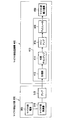
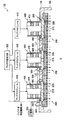
図2を参照しながら、マイクロ波出力部300及びマイクロ波伝送機構400の構成について説明する。図2の左側には、マイクロ波出力部300の内部構成が示されている。図2の右側には、マイクロ波伝送機構400の内部構成が示されている。
The configuration of the
マイクロ波出力部300は、マイクロ波電源305、マイクロ波発振器310及びアンプ315を有している。マイクロ波電源305は、2.45GHz、8.35GHz、5.8GHz、1.98GHz等の周波数のマイクロ波を出力する。マイクロ波電源305は、電磁波源の一例であり、マイクロ波帯の電磁波を出力する。電磁波源は、マイクロ波に限らず、100MHzのRF帯から3GHzのマイクロ波帯までの電磁波を出力する電源である。マイクロ波発振器310は、例えば、2.45GHzの所定周波数のマイクロ波をPLL発振させる。アンプ315は、発振されたマイクロ波を増幅する。
The
マイクロ波伝送機構400は、アンテナモジュール410とマイクロ波導入機構450とを有している。アンテナモジュール410は、位相器412、可変ゲインアンプ414、メインアンプ416及びアイソレータ418を有していて、マイクロ波出力部300から出力されたマイクロ波をマイクロ波導入機構450に伝送する。
The microwave transmission mechanism 400 includes an
位相器412は、スラグチューナによりマイクロ波の位相を変化させるように構成され、これを調整することにより放射特性を変調させることができる。これによれば、指向性を制御してプラズマ分布を変化させることができる。なお、このような放射特性の変調が不要な場合には位相器412は設ける必要はない。
The
可変ゲインアンプ414は、メインアンプ416へ入力するマイクロ波の電力レベルを調整し、プラズマ強度の調整を行う。メインアンプ416は、ソリッドステートアンプを構成する。ソリッドステートアンプは、図示していない入力整合回路、半導体増幅素子、出力整合回路及び高Q共振回路を有する構成とすることができる。
The
アイソレータ418は、アンテナ200で反射してメインアンプ416に戻るマイクロ波の反射波を分離するものであり、サーキュレータとダミーロード(同軸終端器)とを有している。サーキュレータは、アンテナ200で反射したマイクロ波をダミーロードへ導き、ダミーロードは、サーキュレータによって導かれたマイクロ波の反射波を熱に変換する。
The
[プラズマ発生用アンテナの構成]
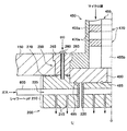
次に、第1実施形態に係るマイクロ波導入機構450及びプラズマ発生用アンテナ200の構成について図3を参照しながら説明する。図3は、第1実施形態に係るマイクロ波導入機構450及びアンテナ200の拡大図(左半分)である。
[Configuration of plasma generation antenna]
Next, configurations of the
マイクロ波導入機構450は、同軸管455及び遅波板480を有している。同軸管455は、筒状の外部導体455a及びその中心に設けられた棒状の内部導体455bからなる同軸状の導波管を有している。同軸管455の下端には、遅波板480を介してアンテナ200が設けられている。同軸管455は、内部導体455bが給電側、外部導体455aが接地側になっている。同軸管455には、チューナ470が設けられている。チューナ470は、2つのスラグ470aを有し、スラグチューナを構成している。スラグ470aは誘電部材の板状体として構成されており、同軸管455の内部導体455bと外部導体455aとの間に円環状に設けられている。チューナ470は、制御部505からの指令に基づき、図示しないアクチュエータによりスラグ470aを上下動させることにより、インピーダンスを調整するようになっている。制御部505は、例えば、同軸管455の終端で50Ωの特性インピーダンスになるようにインピーダンスを調整する。
The
遅波板480は、同軸管455の下面に隣接して設けられている。遅波板480は、円板状の誘電部材から形成されている。遅波板480は、同軸管455を伝送されたマイクロ波を透過し、アンテナ200へと導く。
The
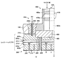
アンテナ200は、シャワーヘッド(ガスシャワーヘッド)210及びシャワーヘッド210に直流電圧を印加する機構(以下、DC印加機構250と称呼する)を有する。シャワーヘッド210は、遅波板480の下面に隣接して設けられている。シャワーヘッド210は、遅波板480より径が大きな円板状であり、アルミニウムや銅等の電気伝導率が高い導電体から形成されている。シャワーヘッド210は、プラズマ空間U側に露出し、露出した下面に表面波を伝搬させる。ここでは、シャワーヘッド210の金属面がプラズマ空間U側に露出している。このように露出した下面に伝搬する表面波を以下、金属表面波という。
The
シャワーヘッド210は、複数のガス穴215と、それらのガス穴215と分離した位置にマイクロ波を通す複数のスロット220を有している。シャワーヘッド210には、その側面を貫通し、シャワーヘッド210の径方向にガス経路225が形成されている。ガスは、ガス供給源600(図1参照)から供給され、ガス供給管605を通ってガス経路225から複数のガス穴215に入り、各ガス穴215から処理容器内に導入される。シャワーヘッド210のプラズマ側に露出した面は、溶射により例えばアルミナ(Al2O3)やイットリア(Y2O3)の被膜290で覆い、導体面がプラズマ空間側に露出しないようにしている。被膜290には、複数のスロット220及び複数のガス穴215に連通する開口が形成される。
The
シャワーヘッド210には図示しない冷却路が設けられ、シャワーヘッド210を冷却するようになっている。シャワーヘッド210は、電気伝導率が高い導電体であるため、マイクロ波の伝送経路であるスロット220からの熱を効率よく処理容器本体側へと逃がすことができる。
The
複数のスロット220は、ガスの供給経路であるガス経路225及び複数のガス穴215と分離した位置に設けられ、シャワーヘッド210の径方向と垂直な方向に貫通している。スロット220の一端は、遅波板480に隣接し、他端は、プラズマ空間U側に開口している。マイクロ波は、同軸管455を伝送し、遅波板480を透過した後、複数のスロット220に通され、プラズマ空間Uに放射される。
The plurality of
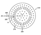
図4は、シャワーヘッド210のプラズマ空間Uに露出した面(下面)を示した図である。複数のガス穴215が概ね均等に配置されている。ガス穴215は、略リング状のスロット220の外周側及び内周側に設けられている。スロット220は、完全なリング状には形成されておらず、4つに区切られた扇状となっている。スロット220が区切られた部分Aには、ガス経路225がスロット220と連通しないように形成され、スロット220の内周側に設けられたガス穴215にガスを供給するようになっている。よって、スロット220には、ガス経路225を通すための区切りが少なくとも一つ必要である。よって、本実施形態では、スロット220は4つであるが、これに限られず、少なくとも一つ以上の区切り部分を有していればよい。
FIG. 4 is a view showing a surface (lower surface) exposed to the plasma space U of the
複数のスロット220は、アンテナ200の中心軸(図3の中心軸O)に対して、軸対称に形成されている。これにより、スロット220からより均一にマイクロ波を放射することができる。
The plurality of
ガス穴215は、プラズマ空間Uに放射されたマイクロ波が当該ガス穴215の内部に入り込まないように細穴となっている。また、スロット220とガス穴215とは、シャワーヘッド210内にて完全に分離されている。これにより、ガス経路225やガス穴215での異常放電を防止することができる。
The
再び図3に戻って、遅波板480とシャワーヘッド210との接触面にはOリング485及びOリング495が設けられ、大気側に設けられたマイクロ波伝送機構400からシャワーヘッド210及び処理空間100の内部を真空シールしている。これにより、プラズマ空間U、スロット220、ガス経路225、ガス穴215の内部を真空状態にすることができる。
Returning to FIG. 3 again, an O-
本実施形態のように、シャワーヘッド210が導電体の場合には、シャワーヘッド210にDC電圧(直流電圧)を印加できる。具体的には、制御部505の指令に従い、DC電源255から出力されたDC電圧は、DC印加機構250に供給される。DC印加機構250は、DC電極260、絶縁部材265及び絶縁シート270を有する。DC電極260は、筒状の導電体260aを有し、筒状の導電体260aを介してシャワーヘッド210に接続され、これにより、シャワーヘッド210にDC電圧を印加する。DC電極260は、筒状の導電体260aの下端に設けられた図示しない絶縁ソケットによりシャワーヘッド210にネジ止めされている。
When the
DC電極260は同軸管455の外部導体455a及び蓋体150に近接している。そこで、DC電極260と同軸管455及びDC電極260と蓋体150をDC的に絶縁するためにDC電極260を絶縁部材265で覆い、DC電極260と同軸管455及びDC電極260と蓋体150を絶縁する。また、シャワーヘッド210と同軸管455及びシャワーヘッド210と蓋体150をDC的に絶縁するために、シャワーヘッド210と同軸管455との間、及びシャワーヘッド210と蓋体150との間に絶縁シート270を挟む。このようにして、処理容器100をDC的に絶縁することにより、DC電圧がシャワーヘッド210のみに印加され、DC電圧のかかる部材をできるだけ少なくすることができる。なお、シャワーヘッド210が絶縁体で形成されている場合には、DC電圧をシャワーヘッド210に印加することはできない。ただし、その場合、RF電圧を印加すれば、同様な効果を期待できる。
The
以上に説明したように、本実施形態に係るプラズマ処理装置10によれは、同軸管455から導入されたマイクロ波は、遅波板480を通り、シャワーヘッド210を貫通して形成された複数のスロット220を通してプラズマ空間Uへ放射される。そのとき、シャワーヘッド210の表面にはプラズマシースを境界条件として分散関係で特徴付けられる波長をもった定在波(金属表面波)が発生し、表面波プラズマに吸収される。ガス供給源600から供給されたガスもまた、シャワーヘッド210を通ってプラズマ空間Uへ導入される。導入されたガスは、表面波プラズマにより励起される。これにより、処理容器100内のプラズマ空間Uに低電子温度かつ高プラズマ密度のプラズマが生成される。生成されたプラズマは、ウエハWのエッチング処理に使われる。プラズマは低電子温度であるため、ウエハWはダメージを受けにくく、また、高プラズマ密度であるため、ウエハWに高速に微細加工を施すことができる。また、シャワーヘッド210を導電体で形成することにより、反応性エッチング等のプロセスを実行することができる。
As described above, according to the
一般的な表面波プラズマ源の場合、アンテナスロットの下部には誘電体が設置され、誘電体にシャワーヘッド構造を作製した場合、電磁波は誘電体を透過するために、その内部で異常放電が発生する可能性が高くなり、一般的な表面波プラズマ源でシャワーヘッド構造を採用することは極めて困難であった。例えば、アルゴンプラズマにおいて、シャワーヘッド空間内に10mmの空間が空いている場合、その距離に沿って約120ボルトの電圧がシャワーヘッド内部に生じると、圧力1Torrでシャワーヘッド内部で異常放電が発生する可能性が高くなる。 In the case of a general surface wave plasma source, a dielectric is installed under the antenna slot, and when a showerhead structure is made in the dielectric, electromagnetic waves pass through the dielectric, causing abnormal discharge inside it. Therefore, it is extremely difficult to adopt a showerhead structure with a general surface wave plasma source. For example, in argon plasma, when a space of 10 mm is vacant in the shower head space, if a voltage of about 120 volts is generated in the shower head along the distance, abnormal discharge occurs in the shower head at a pressure of 1 Torr. The possibility increases.
これに対して、本実施形態に係るプラズマ処理装置10は、シャワーヘッド210が金属などの導電体でできているため、シャワーヘッド210内部に電磁波は進入せず、シャワーヘッド210内部の電界は無いに等しい。そのため、異常放電は起こらない。電磁波とガスは、シャワーヘッド210内部で隔離されており、処理容器100内に入って始めてそれらは接触する。それゆえ、本実施形態に係るプラズマ処理装置10を用いることで、シャワーヘッド210で均一にガスを放出させながら、異常放電無く、表面波プラズマを生成することができる。
On the other hand, in the
また、本実施形態に係るプラズマ処理装置10によれは、シャワーヘッド210にDC電圧を印加しながら、同一のシャワーヘッド210にマイクロ波を印加することができる。これにより、プラズマ処理装置10を多様なプロセスに適用することができる。例えば、マイクロ波が印加されると、シャワーヘッド210の表面に表面波が伝搬する。このとき、シャワーヘッド210の表面にはシース領域が発生し、シースの中を表面波が伝搬する。DC電圧は、そのシースの厚さを制御する。例えば、DC電圧をシャワーヘッド210に印加するとシースを厚く制御することができ、その結果、シャワーヘッド210の表面を伝搬する表面波の伝搬距離を長くすることができる。このようにDC電圧の制御によりプラズマシース電圧を操作することによって、表面波の伝搬距離を制御し、プラズマの電子密度及びラジカル密度を最適化することができる。
In addition, according to the
[スロットの変形例]
アンテナ200に形成されるスロットの変形例について図5を参照しながら説明する。図5の上側、中央、下側には、それぞれ異なる形状のスロット220が図示されている。図5の上側のスロットは、6つのスロット220に区切られている。各スロット220は中央で厚く両端部が薄い同一形状である。隣接するスロット220の両端部は互いに対向している。
[Modification of slot]
A modification of the slot formed in the
図5の中央のスロットは、6つのスロット220に区切られている。各スロット220の中央は両端部と同じ薄さである。各スロット220は、やや湾曲しながら斜め方向に傾いた同一形状である。隣接するスロット220の両端部は互いに対向している。
The central slot in FIG. 5 is divided into six
図5の下側のスロットは、外周側が4つのスロット220に区切られ、内周側も4つのスロット220に区切られた2段のスロット構造となっている。各スロット220は同じ厚さの円弧状であり、同一形状である。外周側のスロット220間の区切りが内周側のスロット220の中央に位置し、内周側のスロット220間の区切りが外周側のスロット220の中央に位置するように配置されている。
The bottom slot in FIG. 5 has a two-stage slot structure in which the outer peripheral side is divided into four
いずれの変形例においても、複数のスロット220は、アンテナ200の中心軸に対して、軸対称に形成されている。これにより、マイクロ波を処理容器100内に均一に放射することができる。また、複数のスロット220は、少なくとも1つ以上の区切り部分を有している。これにより、スロット220の外周側及び内周側に形成された図示しないガス穴215からガスを供給することができる。
In any of the modifications, the plurality of
<第2実施形態>
[プラズマ発生用アンテナの構成]
次に、第2実施形態に係るプラズマ発生用アンテナの構成について図6を参照しながら説明する。図6は、第2実施形態に係るプラズマ発生用アンテナ200の拡大図(左半分)である。第2実施形態に係るプラズマ発生用アンテナ200は、第1実施形態に係るアンテナに替えて、図1のプラズマ処理装置10のアンテナ部分に適用され得る。
Second Embodiment
[Configuration of plasma generation antenna]
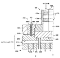
Next, the configuration of the plasma generating antenna according to the second embodiment will be described with reference to FIG. FIG. 6 is an enlarged view (left half) of the
第2実施形態に係る複数のスロット220には、誘電部材220aが充填されている。誘電部材220aとしては、石英等を用いてもよい。これにより、スロット220内にプラズマが進入することを防ぐことができる。
The plurality of
第2実施形態では、例えばアルミニウムで形成されたシャワーヘッド210のプラズマ空間側の露出面には、シリコンの天板700が固定されている。これにより、プラズマによりダメージを受けた天板700を交換することができ、シャワーヘッド210の寿命を延ばすことができる。天板700には、複数のスロット220及び複数のガス穴215に連通する開口が形成される。スロット220と連通する開口には、スロット220と同様に誘電部材220aが充填される。
In the second embodiment, a
<変形例>
上記実施形態の変形例として、シャワーヘッド210がシリコンで形成されている場合を挙げる。その場合には、シャワーヘッド210に溶射を施すことや天板700を設けることなく、図7に示したように、そのままシャワーヘッド210のシリコン表面を露出する。
<Modification>
As a modification of the above embodiment, a case where the
第2実施形態及び変形例の場合にも、シャワーヘッド210にDC電圧を印加しながら、同一のシャワーヘッド210にマイクロ波を印加することができる。これにより、プラズマ処理装置10を多様なプロセスに適用することができる。例えば、マイクロ波が印加されると、シャワーヘッド210の表面に表面波が伝搬する。このとき、シャワーヘッド210の表面にはシース領域が発生し、シースの中を表面波が伝搬する。DC電圧は、そのシースの厚さを制御する。例えば、DC電圧をシャワーヘッド210に印加するとシースを厚く制御することができ、その結果、シャワーヘッド210の表面を伝搬する表面波の伝搬距離を長くすることができる。このようにDC電圧の制御によりプラズマシース電圧を操作することによって、表面波の伝搬距離を制御し、プラズマの電子温度を最適化することができる。さらに、変形例の場合には、DC電圧をシャワーヘッド210に印加すると、シャワーヘッド210からシリコンをたたき出して、これによりエッチングの選択比を高めることも可能となる。
Also in the case of the second embodiment and the modification, it is possible to apply a microwave to the
プラズマ生成時のガス種、圧力及び高周波電力の大きさによっては、スロット220の近傍にプラズマが過度に集中し、プラズマの均一性を乱す恐れがある。しかしながら、以上に説明したように、本実施形態に係るプラズマ処理装置10によれば、スロット220の内部に誘電部材220aが充填されている。このため、スロット220内にプラズマが進入することを防ぐことができる。これにより、プラズマの均一性を高めることができる。また、スロット220内の誘電部材220aにより、スロット内を通るマイクロ波の実効的な波長を短くすることができる。これにより、シャワーヘッド210の厚さを薄くすることができる。
Depending on the gas type, pressure, and high-frequency power at the time of plasma generation, the plasma may be excessively concentrated in the vicinity of the
<第3実施形態>
[プラズマ発生用アンテナの構成]
次に、第3実施形態に係るプラズマ発生用アンテナの構成について図8を参照しながら説明する。図8は、第3実施形態に係るプラズマ発生用アンテナの拡大図(左半分)である。第3実施形態に係るプラズマ発生用アンテナ200は、第1実施形態に係るアンテナに替えて、図1のプラズマ処理装置10のアンテナ部分に適用され得る。
<Third Embodiment>
[Configuration of plasma generation antenna]
Next, the configuration of the plasma generating antenna according to the third embodiment will be described with reference to FIG. FIG. 8 is an enlarged view (left half) of the plasma generating antenna according to the third embodiment. The
第3実施形態に係るシャワーヘッド200のガス経路は、第1のガス経路225a及び第2のガス経路225bに分かれている。第1のガス経路225a及び第2のガス経路225bは、完全に分離されている。第1のガス経路225aは、ガス供給管605aに接続されている。また、第2のガス経路225bは、ガス供給管605bに接続されている。所望のガス1は、ガス供給源600(図1参照)から供給され、ガス供給管605aを通ってガス経路225aから複数のガス穴215に入り、各ガス穴215から処理容器内に導入される。所望のガス2は、ガス供給源600(図1参照)から供給され、ガス供給管605bを通ってガス経路225bから別の複数のガス穴215に入り、各ガス穴215から処理容器内に導入される。これにより、隣接するガス穴から異なる種類のガスを交互に導入することができる。
The gas path of the
以上に説明したように、本実施形態に係るプラズマ処理装置10によれば、シャワーヘッド200中に独立した2つのシャワーヘッド空間(マトリクスシャワー)が設けられ、これにより2系統のガスの流れを制御する。ガスは、各シャワーヘッドから処理容器100に供給され、処理容器内の空間で混合され、2種以上のガスを反応させることができる(ポストミックス)。これによれば、ガス種によってガスの導入位置を最適化でき、所望のプラズマを生成することができる。なお、ガス経路は、2系統に限られず、3種類以上のガスを混合せずに別々に供給可能な3系統以上のガス経路に分かれていてもよい。
As described above, according to the
<第4実施形態>
[プラズマ発生用アンテナの構成]
次に、第4実施形態に係るプラズマ発生用アンテナの構成について図9及び図10を参照しながら説明する。図9は、第4実施形態に係るプラズマ処理装置のアンテナ部分を示した図である。図9では、アンテナ200より下の部分を省略しているが、第4実施形態に係るプラズマ処理装置10は、第1実施形態に係るプラズマ処理装置と同様の構成である。図10は、マイクロ波出力部300及びマイクロ波伝送機構400の構成を示した図である。
<Fourth embodiment>
[Configuration of plasma generation antenna]
Next, the configuration of the plasma generating antenna according to the fourth embodiment will be described with reference to FIGS. FIG. 9 is a view showing an antenna portion of the plasma processing apparatus according to the fourth embodiment. In FIG. 9, the portion below the
第4実施形態に係るプラズマ処理装置10では、3つのアンテナ200が、蓋体150に設けられている。各アンテナ200の基本的構造は第1実施形態にて説明したのでここでは説明を省略する。
In the
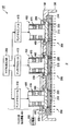
第4実施形態に係るプラズマ処理装置10では、マイクロ波は、図10のマイクロ波出力部300内に示した、マイクロ波電源305から出力され、マイクロ波発振器310及びアンプ315を介して分配器320にて分配される。
In the
具体的には、マイクロ波発振器310は、例えば、2.45GHzの所定周波数のマイクロ波をPLL発振させる。アンプ315は、発振されたマイクロ波を増幅する。分配器320は、増幅されたマイクロ波を複数に分配する。分配器320では、マイクロ波ができるだけ損失されないように、入力側と出力側のインピーダンス整合を取りながらアンプ315で増幅されたマイクロ波を分配する。分配されたマイクロ波は、各アンテナモジュールに410に伝送される。
Specifically, the
本実施形態では、マイクロ波伝送機構400は、分配器320で分配されたマイクロ波を伝送する3つのアンテナモジュール410を有している。各アンテナモジュール410は、マイクロ波を各アンテナモジュール410に接続された同軸管455から処理容器100内に放射し、その内部でマイクロ波を空間合成する。よって、アイソレータ418は小型のものでよく、メインアンプ416に隣接して設けることができる。
In the present embodiment, the microwave transmission mechanism 400 includes three
各アンテナモジュール410の位相器412は、スラグチューナによりマイクロ波の位相を変化させるように構成され、これを調整することにより放射特性を変調させることができる。例えば、アンテナモジュール410毎に位相を調整することにより、指向性を制御してプラズマ分布を変化させることや、隣り合うアンテナモジュール410において90°ずつ位相をずらすようにして円偏波を得ることができる。なお、このような放射特性の変調が不要な場合には位相器412は設ける必要はない。
The
可変ゲインアンプ414は、メインアンプ416へ入力するマイクロ波の電力レベルを調整し、個々のアンテナモジュール410のバラツキの調整やプラズマ強度の調整を行う。可変ゲインアンプ414をアンテナモジュール410毎に変化させることにより、発生するプラズマに分布を生じさせることもできる。
The
メインアンプ416は、ソリッドステートアンプを構成する。ソリッドステートアンプは、図示していない入力整合回路、半導体増幅素子、出力整合回路及び高Q共振回路を有する構成とすることができる。
The
アイソレータ418は、アンテナ200で反射してメインアンプ416に向かうマイクロ波の反射波を分離するものであり、サーキュレータとダミーロード(同軸終端器)とを有している。サーキュレータは、アンテナ200で反射したマイクロ波をダミーロードへ導き、ダミーロードは、サーキュレータによって導かれたマイクロ波の反射波を熱に変換する。アンテナモジュール410から出力されたマイクロ波は、マイクロ波導入機構450に伝送され、アンテナ200に導かれる。
The
なお、本実施形態では、3つのアンテナ200を蓋体150に個別に設け、それぞれにガス供給管605を設けていた、換言すれば、各アンテナ200ごとに独立してシャワーヘッド210が設けられていたが、複数のシャワーヘッド210を蓋体150に設けるよりも、複数のアンテナ200に対して1つのシャワーヘッド210を設けるほうが製作が容易である。したがって、本実施形態の変形例として、例えば図11に示すように、3つのアンテナ200に対して1つのシャワーヘッド210を共通で設けてもよい。かかる場合、共通のシャワーヘッド210に対してガス供給管605が1つ設けられる。なお、図11において、各アンテナ200の基本的構造は、シャワーヘッド210とガス供給管605が複数のアンテナ200に対して共通化されている点を除き図9に示す場合と同様である。
In the present embodiment, the three
また、複数のアンテナ200を1つのシャワーヘッド210に共通して設ける場合、例えばそれぞれ独立した環状のガス経路225を蓋体150の中心軸を中心として同心円状に形成してもよい。かかる場合、各ガス経路225は互いに隔離される。具体的には、例えば図12に示すように、シャワーヘッド210に内外2系統の環状のガス経路225c、225dを形成する。それぞれのガス経路225c、225dには、ガス供給管605がそれぞれ設けられる。こうすることで、プラズマ空間Uへ導入するガスの流速や導入するガスの種類を、シャワーヘッド210の中心側の領域と、外側の領域とでそれぞれ異なるものとすることができる。
When a plurality of
[プラズマ発生用アンテナの動作]
最後に、第1〜第4実施形態にかかるプラズマ処理装置10の動作について、図1を参照しながら説明する。まず、ウエハWを処理容器100内に搬入し、サセプタ105上に載置する。そして、例えばArガス等のプラズマガスは、ガス供給源600から供給され、ガス供給管605を通ってシャワープレート200から処理容器100内に導入される。マイクロ波は、マイクロ波出力部300から出力され、マイクロ波伝送機構400及び遅波板480、スロット220を通って処理容器100内に導入される。マイクロ波の電界エネルギーによりプラズマガスが励起され、プラズマが生成される。
[Operation of plasma generating antenna]
Finally, the operation of the
次に、例えばCl2ガス等のエッチングガスが、ガス供給源600から供給され、複数に分岐したガス供給管605を通ってシャワープレート200から処理容器100内に導入される。エッチングガスは、同様に励起されてプラズマ化する。このようにして形成された処理ガスのプラズマによりウエハWに、例えばエッチング処理が施される。プラズマは低電子温度であるため、ウエハWはダメージを受けにくく、また、高プラズマ密度であるため、ウエハWに高速に微細加工を施すことができる。
Next, for example, an etching gas such as Cl 2 gas is supplied from the gas supply source 600 and introduced into the
特に、第4実施形態にかかるプラズマ処理装置10では、マイクロ波発振器310から発振されたマイクロ波は、アンプ315で増幅された後、分配器320により複数に分配される。分配されたマイクロ波は、複数のアンテナモジュール410に導かれる。各アンテナモジュール410において、このように複数に分配されたマイクロ波は、ソリッドステートアンプを構成するメインアンプ416で個別に増幅し、各マイクロ波導入機構450に伝送される。各マイクロ波導入機構450では、同軸管455を用いてマイクロ波が遅波板480に伝送される。遅波板480を透過したマイクロ波は、各シャワーヘッド200のスロット200から処理容器内に放射される。
In particular, in the
以上、各実施形態によれば、ガス及び電磁波を分離して供給可能な、プラズマ発生用アンテナ200及びプラズマ処理装置10を提供することができる。
As described above, according to each embodiment, it is possible to provide the
以上、添付図面を参照しながら本発明の好適な実施形態について詳細に説明したが、本発明はかかる例に限定されない。本発明の属する技術の分野における通常の知識を有する者であれば、特許請求の範囲に記載された技術的思想の範疇において、各種の変更例または修正例に想到し得ることは明らかであり、これらについても、当然に本発明の技術的範囲に属するものと了解される。 The preferred embodiments of the present invention have been described in detail above with reference to the accompanying drawings, but the present invention is not limited to such examples. It is obvious that a person having ordinary knowledge in the technical field to which the present invention pertains can make various changes or modifications within the scope of the technical idea described in the claims. Of course, it is understood that these also belong to the technical scope of the present invention.
例えば、上記実施形態では、プラズマ処理装置内にて実行されるプラズマ処理としてエッチング処理を例に挙げて説明したが、本発明はかかる例に限定されない。例えば、本発明に係るプラズマ処理装置は、成膜やアッシング等、あらゆるプラズマ処理を実行可能である。 For example, in the above embodiment, the etching process is described as an example of the plasma process performed in the plasma processing apparatus, but the present invention is not limited to such an example. For example, the plasma processing apparatus according to the present invention can execute any plasma processing such as film formation and ashing.
また、本発明に係るプラズマ発生用アンテナは、上記実施形態に示したマイクロ波プラズマ処理装置に限られず、誘導結合型ICP(Inductively Coupled Plasma)のプラズマ処理装置、容量結合型のプラズマ処理装置等いずれのプラズマ処理装置にも使用することができる。そして、本発明に係るプラズマ処理装置は、表面波プラズマを使うプロセス、ICPプラズマを使うプロセス、CCPプラズマを使うプロセスに適用可能である。 Further, the plasma generating antenna according to the present invention is not limited to the microwave plasma processing apparatus described in the above embodiment, and any of inductively coupled ICP (Inductively Coupled Plasma) plasma processing apparatus, capacitively coupled plasma processing apparatus, etc. It can also be used for the plasma processing apparatus. The plasma processing apparatus according to the present invention can be applied to a process using surface wave plasma, a process using ICP plasma, and a process using CCP plasma.
また、各実施形態では、プラズマ処理装置に取り付けられたプラズマ発生用アンテナは1つ又は3つであった。しかしながら、本発明に係るプラズマ処理装置に取り付けるプラズマ発生用アンテナの数は、これに限定されず、2つ又は4つ又はそれ以上であってもよい。ただし、ウエハWをイオンによってたたく工程を含むプロセスの場合には、複数のプラズマ発生用アンテナを持ったプラズマ処理装置が好ましい。一方、ウエハWをラジカルで反応させるプロセスの場合には、1つのプラズマ発生用アンテナを持ったプラズマ処理装置が好ましい。 In each embodiment, the number of plasma generating antennas attached to the plasma processing apparatus is one or three. However, the number of plasma generating antennas attached to the plasma processing apparatus according to the present invention is not limited to this, and may be two, four, or more. However, in the case of a process including a step of hitting the wafer W with ions, a plasma processing apparatus having a plurality of plasma generating antennas is preferable. On the other hand, in the process of reacting the wafer W with radicals, a plasma processing apparatus having one plasma generating antenna is preferable.
また、本発明に係るプラズマ処理装置の処理容器は、円筒状に限られず、例えば6角形や4角形でもよい。従って、本発明に係るプラズマ処理装置にて処理される被処理体は、円盤状の半導体ウエハに限らず、例えば、矩形の基板であってもよい。 Further, the processing container of the plasma processing apparatus according to the present invention is not limited to a cylindrical shape, and may be, for example, a hexagonal shape or a rectangular shape. Therefore, the workpiece to be processed by the plasma processing apparatus according to the present invention is not limited to the disk-shaped semiconductor wafer, but may be a rectangular substrate, for example.
10 プラズマ処理装置
100 処理容器
105 サセプタ
150 蓋体
200 プラズマ発生用アンテナ
210 シャワーヘッド
215 ガス穴
220 スロット
225 ガス経路
225a 第1のガス経路
225b 第2のガス経路
250 DC印加機構
255 DC電源
260 DC電極
300 マイクロ波出力部
400 マイクロ波伝送機構
410 アンテナモジュール
450 マイクロ波導入機構
455 同軸管
455a 外部導体
455b 内部導体
480 遅波板
500 制御装置
505 制御部
600 ガス供給源
U プラズマ空間
DESCRIPTION OF
Claims (15)
供給された電磁波を透過する遅波板と、
前記遅波板に隣接して設けられたシャワーヘッドを有するプラズマ発生用アンテナと、を備え、
前記シャワーヘッドは、導電体で形成され、複数のガス穴が形成され、該複数のガス穴と分離した位置に電磁波を通す複数のスロットを有することを特徴とするプラズマ処理装置。 A processing vessel in which plasma processing is performed;
A slow wave plate that transmits the supplied electromagnetic wave;
A plasma generating antenna having a shower head provided adjacent to the slow wave plate,
The plasma processing apparatus, wherein the shower head is formed of a conductor, has a plurality of gas holes, and has a plurality of slots through which electromagnetic waves pass at positions separated from the gas holes.
Priority Applications (5)
| Application Number | Priority Date | Filing Date | Title |
|---|---|---|---|
| JP2012072759A JP2012216525A (en) | 2011-03-31 | 2012-03-28 | Plasma processing apparatus and plasma generation antenna |
| KR1020120033519A KR20120112261A (en) | 2011-03-31 | 2012-03-30 | Plasma processing apparatus and plasma generation antenna |
| TW101111240A TW201304617A (en) | 2011-03-31 | 2012-03-30 | Plasma processing apparatus and plasma generation antenna |
| US13/435,552 US9543123B2 (en) | 2011-03-31 | 2012-03-30 | Plasma processing apparatus and plasma generation antenna |
| CN2012100933940A CN102737944A (en) | 2011-03-31 | 2012-03-31 | Plasma processing apparatus and plasma generation antenna |
Applications Claiming Priority (3)
| Application Number | Priority Date | Filing Date | Title |
|---|---|---|---|
| JP2011078029 | 2011-03-31 | ||
| JP2011078029 | 2011-03-31 | ||
| JP2012072759A JP2012216525A (en) | 2011-03-31 | 2012-03-28 | Plasma processing apparatus and plasma generation antenna |
Publications (2)
| Publication Number | Publication Date |
|---|---|
| JP2012216525A true JP2012216525A (en) | 2012-11-08 |
| JP2012216525A5 JP2012216525A5 (en) | 2015-05-07 |
Family
ID=47269094
Family Applications (1)
| Application Number | Title | Priority Date | Filing Date |
|---|---|---|---|
| JP2012072759A Pending JP2012216525A (en) | 2011-03-31 | 2012-03-28 | Plasma processing apparatus and plasma generation antenna |
Country Status (3)
| Country | Link |
|---|---|
| JP (1) | JP2012216525A (en) |
| KR (1) | KR20120112261A (en) |
| TW (1) | TW201304617A (en) |
Cited By (7)
| Publication number | Priority date | Publication date | Assignee | Title |
|---|---|---|---|---|
| JP2015118739A (en) * | 2013-12-16 | 2015-06-25 | 東京エレクトロン株式会社 | Microwave plasma source and plasma processing apparatus |
| JP2017123346A (en) * | 2017-03-28 | 2017-07-13 | 東京エレクトロン株式会社 | Microwave radiation antenna, microwave plasma source, and plasma processing device |
| US9991097B2 (en) | 2016-10-25 | 2018-06-05 | Tokyo Electron Limited | Plasma processing apparatus |
| JP2018195548A (en) * | 2017-05-16 | 2018-12-06 | 東京エレクトロン株式会社 | Plasma processing device |
| KR20190027742A (en) * | 2017-09-07 | 2019-03-15 | 도쿄엘렉트론가부시키가이샤 | Plasma processing apparatus |
| KR20190070283A (en) | 2017-12-12 | 2019-06-20 | 도쿄엘렉트론가부시키가이샤 | Antenna and plasma film forming apparatus |
| US10804078B2 (en) | 2016-04-26 | 2020-10-13 | Tokyo Electron Limited | Plasma processing apparatus and gas introduction mechanism |
Families Citing this family (4)
| Publication number | Priority date | Publication date | Assignee | Title |
|---|---|---|---|---|
| KR101485964B1 (en) * | 2013-01-16 | 2015-01-27 | 주식회사 아이브이웍스 | Microwave plasma reactor |
| JP6338462B2 (en) * | 2013-09-11 | 2018-06-06 | 東京エレクトロン株式会社 | Plasma processing equipment |
| KR101588609B1 (en) * | 2014-06-16 | 2016-01-27 | 주식회사 윈텔 | Plasma generation apparatus |
| JP6580830B2 (en) * | 2015-01-22 | 2019-09-25 | 株式会社Screenホールディングス | Plasma processing equipment |
Citations (7)
| Publication number | Priority date | Publication date | Assignee | Title |
|---|---|---|---|---|
| JPS63263725A (en) * | 1987-04-22 | 1988-10-31 | Hitachi Ltd | Plasma treatment apparatus |
| JPH07335633A (en) * | 1994-06-14 | 1995-12-22 | Nec Corp | Plasma treating device |
| JP2007221116A (en) * | 2006-01-20 | 2007-08-30 | Tokyo Electron Ltd | Plasma processing apparatus |
| JP2009301802A (en) * | 2008-06-11 | 2009-12-24 | Tokyo Electron Ltd | Plasma processing apparatus |
| JP2010087227A (en) * | 2008-09-30 | 2010-04-15 | Tokyo Electron Ltd | Plasma processing apparatus |
| JP2010244805A (en) * | 2009-04-03 | 2010-10-28 | Tokyo Electron Ltd | Plasma treatment device |
| WO2010140526A1 (en) * | 2009-06-01 | 2010-12-09 | 東京エレクトロン株式会社 | Plasma processing apparatus and power feeding method for plasma processing apparatus |
-
2012
- 2012-03-28 JP JP2012072759A patent/JP2012216525A/en active Pending
- 2012-03-30 KR KR1020120033519A patent/KR20120112261A/en not_active Application Discontinuation
- 2012-03-30 TW TW101111240A patent/TW201304617A/en unknown
Patent Citations (7)
| Publication number | Priority date | Publication date | Assignee | Title |
|---|---|---|---|---|
| JPS63263725A (en) * | 1987-04-22 | 1988-10-31 | Hitachi Ltd | Plasma treatment apparatus |
| JPH07335633A (en) * | 1994-06-14 | 1995-12-22 | Nec Corp | Plasma treating device |
| JP2007221116A (en) * | 2006-01-20 | 2007-08-30 | Tokyo Electron Ltd | Plasma processing apparatus |
| JP2009301802A (en) * | 2008-06-11 | 2009-12-24 | Tokyo Electron Ltd | Plasma processing apparatus |
| JP2010087227A (en) * | 2008-09-30 | 2010-04-15 | Tokyo Electron Ltd | Plasma processing apparatus |
| JP2010244805A (en) * | 2009-04-03 | 2010-10-28 | Tokyo Electron Ltd | Plasma treatment device |
| WO2010140526A1 (en) * | 2009-06-01 | 2010-12-09 | 東京エレクトロン株式会社 | Plasma processing apparatus and power feeding method for plasma processing apparatus |
Cited By (10)
| Publication number | Priority date | Publication date | Assignee | Title |
|---|---|---|---|---|
| JP2015118739A (en) * | 2013-12-16 | 2015-06-25 | 東京エレクトロン株式会社 | Microwave plasma source and plasma processing apparatus |
| US10804078B2 (en) | 2016-04-26 | 2020-10-13 | Tokyo Electron Limited | Plasma processing apparatus and gas introduction mechanism |
| US9991097B2 (en) | 2016-10-25 | 2018-06-05 | Tokyo Electron Limited | Plasma processing apparatus |
| JP2017123346A (en) * | 2017-03-28 | 2017-07-13 | 東京エレクトロン株式会社 | Microwave radiation antenna, microwave plasma source, and plasma processing device |
| JP2018195548A (en) * | 2017-05-16 | 2018-12-06 | 東京エレクトロン株式会社 | Plasma processing device |
| JP7058485B2 (en) | 2017-05-16 | 2022-04-22 | 東京エレクトロン株式会社 | Plasma processing equipment |
| KR20190027742A (en) * | 2017-09-07 | 2019-03-15 | 도쿄엘렉트론가부시키가이샤 | Plasma processing apparatus |
| KR102107310B1 (en) * | 2017-09-07 | 2020-05-06 | 도쿄엘렉트론가부시키가이샤 | Plasma processing apparatus |
| KR20190070283A (en) | 2017-12-12 | 2019-06-20 | 도쿄엘렉트론가부시키가이샤 | Antenna and plasma film forming apparatus |
| US10991549B2 (en) | 2017-12-12 | 2021-04-27 | Tokyo Electron Limited | Antenna and plasma deposition apparatus |
Also Published As
| Publication number | Publication date |
|---|---|
| KR20120112261A (en) | 2012-10-11 |
| TW201304617A (en) | 2013-01-16 |
Similar Documents
| Publication | Publication Date | Title |
|---|---|---|
| US9543123B2 (en) | Plasma processing apparatus and plasma generation antenna | |
| JP6046052B2 (en) | Plasma generating antenna, plasma processing apparatus, and plasma processing method | |
| JP2012216525A (en) | Plasma processing apparatus and plasma generation antenna | |
| TWI681073B (en) | Plasma treatment device | |
| JP6096547B2 (en) | Plasma processing apparatus and shower plate | |
| TWI430358B (en) | Microwave plasma source and plasma processing device | |
| JP5805227B2 (en) | Plasma processing equipment | |
| JP5376816B2 (en) | Microwave introduction mechanism, microwave plasma source, and microwave plasma processing apparatus | |
| JP4677918B2 (en) | Plasma processing apparatus and plasma processing method | |
| JP6509049B2 (en) | Microwave plasma source and plasma processing apparatus | |
| WO2010004997A1 (en) | Plasma processing apparatus | |
| US20110150719A1 (en) | Microwave introduction mechanism, microwave plasma source and microwave plasma processing apparatus | |
| KR102000355B1 (en) | Plasma processing apparatus | |
| JP2006244891A (en) | Microwave plasma processing device | |
| JP6624833B2 (en) | Microwave plasma source and plasma processing apparatus | |
| JP2018006718A (en) | Microwave plasma processing device | |
| JP2010170974A (en) | Plasma source and plasma treatment device | |
| JP2006040638A (en) | Plasma processing device | |
| JP6671230B2 (en) | Plasma processing device and gas introduction mechanism | |
| US10777389B2 (en) | Plasma processing apparatus and plasma processing method | |
| JP6700128B2 (en) | Microwave plasma processing equipment | |
| JP6700127B2 (en) | Microwave plasma processing equipment | |
| JP5916467B2 (en) | Microwave radiation antenna, microwave plasma source, and plasma processing apparatus |
Legal Events
| Date | Code | Title | Description |
|---|---|---|---|
| A521 | Written amendment |
Free format text: JAPANESE INTERMEDIATE CODE: A523 Effective date: 20150318 |
|
| A621 | Written request for application examination |
Free format text: JAPANESE INTERMEDIATE CODE: A621 Effective date: 20150318 |
|
| A977 | Report on retrieval |
Free format text: JAPANESE INTERMEDIATE CODE: A971007 Effective date: 20160215 |
|
| A131 | Notification of reasons for refusal |
Free format text: JAPANESE INTERMEDIATE CODE: A131 Effective date: 20160223 |
|
| A521 | Written amendment |
Free format text: JAPANESE INTERMEDIATE CODE: A523 Effective date: 20160421 |
|
| A02 | Decision of refusal |
Free format text: JAPANESE INTERMEDIATE CODE: A02 Effective date: 20161011 |