JP2012212870A - Photoconductive element - Google Patents
Photoconductive element Download PDFInfo
- Publication number
- JP2012212870A JP2012212870A JP2012048692A JP2012048692A JP2012212870A JP 2012212870 A JP2012212870 A JP 2012212870A JP 2012048692 A JP2012048692 A JP 2012048692A JP 2012048692 A JP2012048692 A JP 2012048692A JP 2012212870 A JP2012212870 A JP 2012212870A
- Authority
- JP
- Japan
- Prior art keywords
- electromagnetic wave
- region
- semiconductor layer
- photoconductive element
- light
- Prior art date
- Legal status (The legal status is an assumption and is not a legal conclusion. Google has not performed a legal analysis and makes no representation as to the accuracy of the status listed.)
- Abandoned
Links
- 239000004065 semiconductor Substances 0.000 claims abstract description 84
- 238000001514 detection method Methods 0.000 claims abstract description 18
- 239000003362 semiconductor superlattice Substances 0.000 claims description 16
- 230000004888 barrier function Effects 0.000 claims description 10
- 230000031700 light absorption Effects 0.000 claims description 10
- 239000000463 material Substances 0.000 claims description 6
- 230000001678 irradiating effect Effects 0.000 claims description 3
- 239000000203 mixture Substances 0.000 claims description 2
- 230000035945 sensitivity Effects 0.000 abstract description 4
- 230000005284 excitation Effects 0.000 description 17
- 229910000530 Gallium indium arsenide Inorganic materials 0.000 description 9
- 238000000034 method Methods 0.000 description 7
- 239000000969 carrier Substances 0.000 description 6
- 230000003287 optical effect Effects 0.000 description 6
- 238000010586 diagram Methods 0.000 description 5
- 239000000758 substrate Substances 0.000 description 5
- 239000013078 crystal Substances 0.000 description 4
- 230000005684 electric field Effects 0.000 description 4
- 239000000523 sample Substances 0.000 description 4
- 238000001228 spectrum Methods 0.000 description 4
- 238000000862 absorption spectrum Methods 0.000 description 3
- 239000000835 fiber Substances 0.000 description 3
- 238000010521 absorption reaction Methods 0.000 description 2
- 239000003814 drug Substances 0.000 description 2
- 238000003384 imaging method Methods 0.000 description 2
- 238000001451 molecular beam epitaxy Methods 0.000 description 2
- 238000001328 terahertz time-domain spectroscopy Methods 0.000 description 2
- 229910000980 Aluminium gallium arsenide Inorganic materials 0.000 description 1
- 229910001218 Gallium arsenide Inorganic materials 0.000 description 1
- 230000001133 acceleration Effects 0.000 description 1
- 238000004458 analytical method Methods 0.000 description 1
- 238000000137 annealing Methods 0.000 description 1
- 239000012237 artificial material Substances 0.000 description 1
- 229910052790 beryllium Inorganic materials 0.000 description 1
- ATBAMAFKBVZNFJ-UHFFFAOYSA-N beryllium atom Chemical compound [Be] ATBAMAFKBVZNFJ-UHFFFAOYSA-N 0.000 description 1
- 239000012141 concentrate Substances 0.000 description 1
- 230000000694 effects Effects 0.000 description 1
- 230000005672 electromagnetic field Effects 0.000 description 1
- 150000002500 ions Chemical class 0.000 description 1
- 239000007769 metal material Substances 0.000 description 1
- 230000004048 modification Effects 0.000 description 1
- 238000012986 modification Methods 0.000 description 1
- 230000000704 physical effect Effects 0.000 description 1
- 230000005855 radiation Effects 0.000 description 1
- 238000005070 sampling Methods 0.000 description 1
- 238000004611 spectroscopical analysis Methods 0.000 description 1
- 239000000126 substance Substances 0.000 description 1
Images


Classifications
-
- G—PHYSICS
- G01—MEASURING; TESTING
- G01J—MEASUREMENT OF INTENSITY, VELOCITY, SPECTRAL CONTENT, POLARISATION, PHASE OR PULSE CHARACTERISTICS OF INFRARED, VISIBLE OR ULTRAVIOLET LIGHT; COLORIMETRY; RADIATION PYROMETRY
- G01J3/00—Spectrometry; Spectrophotometry; Monochromators; Measuring colours
- G01J3/28—Investigating the spectrum
- G01J3/42—Absorption spectrometry; Double beam spectrometry; Flicker spectrometry; Reflection spectrometry
-
- B—PERFORMING OPERATIONS; TRANSPORTING
- B82—NANOTECHNOLOGY
- B82Y—SPECIFIC USES OR APPLICATIONS OF NANOSTRUCTURES; MEASUREMENT OR ANALYSIS OF NANOSTRUCTURES; MANUFACTURE OR TREATMENT OF NANOSTRUCTURES
- B82Y20/00—Nanooptics, e.g. quantum optics or photonic crystals
-
- H—ELECTRICITY
- H01—ELECTRIC ELEMENTS
- H01L—SEMICONDUCTOR DEVICES NOT COVERED BY CLASS H10
- H01L31/00—Semiconductor devices sensitive to infrared radiation, light, electromagnetic radiation of shorter wavelength or corpuscular radiation and specially adapted either for the conversion of the energy of such radiation into electrical energy or for the control of electrical energy by such radiation; Processes or apparatus specially adapted for the manufacture or treatment thereof or of parts thereof; Details thereof
- H01L31/0248—Semiconductor devices sensitive to infrared radiation, light, electromagnetic radiation of shorter wavelength or corpuscular radiation and specially adapted either for the conversion of the energy of such radiation into electrical energy or for the control of electrical energy by such radiation; Processes or apparatus specially adapted for the manufacture or treatment thereof or of parts thereof; Details thereof characterised by their semiconductor bodies
- H01L31/0352—Semiconductor devices sensitive to infrared radiation, light, electromagnetic radiation of shorter wavelength or corpuscular radiation and specially adapted either for the conversion of the energy of such radiation into electrical energy or for the control of electrical energy by such radiation; Processes or apparatus specially adapted for the manufacture or treatment thereof or of parts thereof; Details thereof characterised by their semiconductor bodies characterised by their shape or by the shapes, relative sizes or disposition of the semiconductor regions
- H01L31/035236—Superlattices; Multiple quantum well structures
-
- H—ELECTRICITY
- H01—ELECTRIC ELEMENTS
- H01L—SEMICONDUCTOR DEVICES NOT COVERED BY CLASS H10
- H01L31/00—Semiconductor devices sensitive to infrared radiation, light, electromagnetic radiation of shorter wavelength or corpuscular radiation and specially adapted either for the conversion of the energy of such radiation into electrical energy or for the control of electrical energy by such radiation; Processes or apparatus specially adapted for the manufacture or treatment thereof or of parts thereof; Details thereof
- H01L31/08—Semiconductor devices sensitive to infrared radiation, light, electromagnetic radiation of shorter wavelength or corpuscular radiation and specially adapted either for the conversion of the energy of such radiation into electrical energy or for the control of electrical energy by such radiation; Processes or apparatus specially adapted for the manufacture or treatment thereof or of parts thereof; Details thereof in which radiation controls flow of current through the device, e.g. photoresistors
- H01L31/09—Devices sensitive to infrared, visible or ultraviolet radiation
Abstract
Description
本発明は、励起光の照射によって電磁波を発生・検出する光伝導素子及び電磁波発生・検出装置(発生・検出は、発生と検出の少なくとも一方を行うことが可能なことを意味する)に関する。 The present invention relates to a photoconductive element and an electromagnetic wave generation / detection device (generation / detection means that at least one of generation and detection can be performed) that generates / detects an electromagnetic wave by irradiation of excitation light.
ミリ波帯からテラヘルツ波帯まで(30GHz以上30THz以下)の周波数帯域内にある成分を含む電磁波(本明細書では、単にテラヘルツ波とも呼ぶ)は、以下の様な特徴を持つ。第一に、X線の様に非金属物質を透過する。第二に、生体分子や医薬品などに固有の吸収スペクトルがこの周波数帯に多数存在する。第三に、多くのイメージング用途に必要な空間分解能を有する。以上の特徴から、テラヘルツ波の応用分野として、物質内部の分光分析技術、X線に代わる安全な透視イメージング装置、生体分子や医薬品の解析技術などが開発されている。 An electromagnetic wave including a component in the frequency band from the millimeter wave band to the terahertz wave band (30 GHz or more and 30 THz or less) (also simply referred to as a terahertz wave in this specification) has the following characteristics. First, it passes through non-metallic materials like X-rays. Second, there are many absorption spectra unique to biomolecules and pharmaceuticals in this frequency band. Third, it has the spatial resolution required for many imaging applications. In view of the above characteristics, as an application field of terahertz waves, a spectroscopic analysis technique inside a substance, a safe fluoroscopic imaging apparatus replacing X-rays, an analysis technique for biomolecules and pharmaceuticals, and the like have been developed.
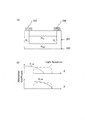
テラヘルツ波の発生及び検出の方法として、さまざまな方法があるが、広く用いられている方法は、光伝導素子を用いる方法である(特許文献1参照)。光伝導素子は、移動度が比較的大きくてキャリア寿命がピコ秒以下という特殊な半導体と、その上に設けられた二つの電極とで構成される。電極間に電圧を印加した状態で電極間のギャップに光照射を行うと、ピコ秒オーダーの電流が電極間を流れ、テラヘルツ波が放射される。反対に、電極間に電圧を印加せずに電極間のギャップに光照射を行うと、テラヘルツ波の作る瞬時電界がサンプリングされて、電流として検知される。テラヘルツ波の出力及び検出感度を増大する為には、上記の特殊な半導体(これを光伝導膜とも呼ぶ)の抵抗率が高い方が好ましく、これを解決する為の光伝導素子が特許文献1に開示されている。図7に示すこの光伝導素子は、InP基板11、InGaAsによる光伝導膜12、電極13、14とで構成される。InGaAs12はFeイオンが注入され、抵抗率を上昇させた光伝導膜が形成されている。光伝導膜12には電源2によって電圧が印加されており、図示しないレーザ装置などから幅がフェムト秒の短いパルス光3(波長約1.5μm)を照射すると、電極13、14を兼ねたアンテナからテラヘルツ波4が放射される。
There are various methods for generating and detecting terahertz waves, and a widely used method is a method using a photoconductive element (see Patent Document 1). The photoconductive element is composed of a special semiconductor having relatively high mobility and a carrier lifetime of picoseconds or less, and two electrodes provided thereon. When light is applied to the gap between the electrodes while a voltage is applied between the electrodes, a picosecond order current flows between the electrodes, and a terahertz wave is emitted. On the other hand, when light is applied to the gap between the electrodes without applying a voltage between the electrodes, the instantaneous electric field generated by the terahertz wave is sampled and detected as a current. In order to increase the output and detection sensitivity of the terahertz wave, it is preferable that the resistivity of the special semiconductor (which is also referred to as a photoconductive film) is high, and a photoconductive element for solving this problem is disclosed in Patent Document 1. Is disclosed. This photoconductive element shown in FIG. 7 includes an InP substrate 11, a photoconductive film 12 made of InGaAs, and
しかしながら、従来の光伝導素子における光伝導層の高抵抗率化には限界があった。この限界は、使用する半導体材料のバンドギャップで概ね決定され、バンドキャップが小さいほど熱励起キャリアが増加し、高抵抗率化が難しいことに起因する。ゆえに、1.0μm帯や1.5μm帯などのファイバーレーザの波長領域(比較的小さなバンドギャップに対応する波長領域)に対応する光伝導素子の出力及び検出感度の増大には、材料に依存する限界があった。 However, there is a limit to increasing the resistivity of the photoconductive layer in the conventional photoconductive element. This limit is largely determined by the band gap of the semiconductor material used, and is caused by the fact that the smaller the band cap, the more thermally excited carriers increase, making it difficult to increase the resistivity. Therefore, the output of the photoconductive element corresponding to the wavelength region (wavelength region corresponding to a relatively small band gap) of the fiber laser such as the 1.0 μm band and the 1.5 μm band depends on the material. There was a limit.
上記課題に鑑み、本発明の光伝導素子は、光を照射すると電磁波を発生・検出し得る光伝導素子であって、光が照射された際に抵抗率が変化することにより電磁波を発生・検出し得る半導体層を有する光伝導層と、前記半導体層と接して配された複数の電極を備える。前記半導体層は、抵抗率(単位体積あたりの抵抗)が、前記電極が接する前記半導体層の面と交わる方向に変化する。また、前記半導体層は、前記半導体層において第1の領域及び前記第1の領域より前記交わる方向に前記電極から離れた第2の領域をとるとき、前記第1の領域での抵抗率が前記第2の領域での抵抗率より大きい。 In view of the above problems, the photoconductive element of the present invention is a photoconductive element that can generate and detect electromagnetic waves when irradiated with light, and generates and detects electromagnetic waves by changing the resistivity when irradiated with light. And a plurality of electrodes arranged in contact with the semiconductor layer. The semiconductor layer has a resistivity (resistance per unit volume) that changes in a direction that intersects the surface of the semiconductor layer in contact with the electrode. In addition, when the semiconductor layer takes a first region in the semiconductor layer and a second region away from the electrode in the intersecting direction from the first region, the resistivity in the first region is Greater than the resistivity in the second region.
本発明によれば、光伝導層をなす半導体層の抵抗率が、複数の電極が接する半導体層の面と交わる方向(厚みの方向で、通常は垂直な方向)に変化する。更に、光伝導層をなす半導体層の電極から第1の厚みの領域での抵抗率が、第1の厚みより大きな第2の厚みの領域での抵抗率より大きい。このため、電極からの電流は、第1の厚みの領域に集中せず、素子全体として高抵抗化される。よって、出力及び検出感度が増大した光伝導素子を提供することができる。また、第1の厚みの領域での光吸収波長が、第2の厚みの領域での光吸収波長より短い構成にすることが容易にできる。ゆえに、励起光を効率良く吸収し、光伝導素子として出力及び検出感度を増大することができる。 According to the present invention, the resistivity of the semiconductor layer forming the photoconductive layer changes in a direction (thickness direction, usually a vertical direction) intersecting with the surface of the semiconductor layer in contact with the plurality of electrodes. Further, the resistivity in the first thickness region from the electrode of the semiconductor layer forming the photoconductive layer is larger than the resistivity in the second thickness region larger than the first thickness. For this reason, the current from the electrode is not concentrated in the region of the first thickness, and the resistance of the entire element is increased. Therefore, it is possible to provide a photoconductive element with increased output and detection sensitivity. In addition, the light absorption wavelength in the first thickness region can be easily made shorter than the light absorption wavelength in the second thickness region. Therefore, it is possible to efficiently absorb the excitation light and increase the output and detection sensitivity as a photoconductive element.
本発明の光伝導素子において重要なことは、光伝導層をなす半導体層の抵抗率が、次の条件を満たすことである。まず、複数の電極が接する半導体層の面と交わる方向に抵抗率が変化することである。更に、半導体層において任意に第1の領域及びこの領域より前記交わる方向に電極から離れた第2の領域をとるとき、第1の領域での抵抗率が第2の領域での抵抗率より大きいことである。この領域は、巨視的なスケール(半導体においては、例えば100nm程度以上)の厚さを前記交わる方向に持つ領域であり、抵抗率はそこでの平均的な抵抗率を指す。 What is important in the photoconductive element of the present invention is that the resistivity of the semiconductor layer forming the photoconductive layer satisfies the following condition. First, the resistivity changes in a direction intersecting with the surface of the semiconductor layer in contact with the plurality of electrodes. Further, when the semiconductor layer is arbitrarily provided with the first region and the second region separated from the electrode in the intersecting direction from this region, the resistivity in the first region is larger than the resistivity in the second region. That is. This region is a region having a macroscopic thickness (for example, about 100 nm or more in a semiconductor) in the intersecting direction, and the resistivity indicates an average resistivity there.
典型的な実施形態では、抵抗率及び吸収波長が異なる二つ以上の半導体層を用いて、素子全体としては効果的に素子抵抗が高くなるように電極を配置する。つまり、電極に近い第1の厚みの領域に高抵抗率の半導体層、電極から遠い第2の厚みの領域にこれよりも抵抗率が低い半導体層を配置する。また、光吸収時もこの関係が満たされるように励起光の波長成分を分割し、第1の厚みの領域に励起光の短波長成分を光吸収する半導体層、第2の厚みの領域にこれよりも波長の長い長波長成分を光吸収する半導体層をこの順に配置する。光入射側からこの順で配置すると、励起光を効率良く吸収することもできる。光伝導層は、ポンプ光やプローブ光が照射されると、光伝導層の抵抗率が変化し、その際の光スイッチングに基づいて電磁波を発生・検出する機能を有している。当然、光伝導層を構成している半導体層自体の抵抗率も変化している。 In a typical embodiment, two or more semiconductor layers having different resistivities and absorption wavelengths are used, and the electrodes are arranged so that the element resistance is effectively increased as the whole element. That is, a high resistivity semiconductor layer is disposed in a first thickness region close to the electrode, and a lower resistivity semiconductor layer is disposed in a second thickness region far from the electrode. In addition, the wavelength component of the excitation light is divided so that this relationship is satisfied also during light absorption, and the semiconductor layer that absorbs the short wavelength component of the excitation light in the first thickness region and the second thickness region. A semiconductor layer that absorbs a long-wavelength component having a longer wavelength than that is disposed in this order. When arranged in this order from the light incident side, the excitation light can also be efficiently absorbed. The photoconductive layer has a function of generating and detecting electromagnetic waves based on optical switching at the time when the resistivity of the photoconductive layer changes when irradiated with pump light or probe light. Naturally, the resistivity of the semiconductor layer itself constituting the photoconductive layer also changes.
以下、図を用いて本発明の実施形態ないし実施例を説明する。
(実施形態1)
実施形態1に係る光伝導素子について、図1、図2を用いて説明する。図1は、本実施形態に係る光伝導素子の断面図、図2は、素子構成と等価回路エレメントの対応を示す図である。
Embodiments and examples of the present invention will be described below with reference to the drawings.
(Embodiment 1)
The photoconductive element according to Embodiment 1 will be described with reference to FIGS. FIG. 1 is a cross-sectional view of a photoconductive element according to the present embodiment, and FIG. 2 is a diagram showing the correspondence between the element configuration and equivalent circuit elements.
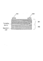
本実施形態の光伝導素子は、光伝導膜となる半導体層101、102のスタック及び半導体層101と接した二電極103、104を含む。半導体層101は、比較的高抵抗率の半導体で構成され、例えばバンドギャップは比較的大きい材料を用いる。これと比較して半導体層102は比較的低抵抗率の半導体から構成され、例えばバンドギャップの比較的小さい材料を用いる。二電極103、104の接する半導体層の面からみた上記構造の等価回路は図2(a)のように表すことができる。すなわち、電極から第一の厚み201までの抵抗率を積分した抵抗がR101(半導体層101の抵抗)、第一の厚み201から第二の厚み202までの抵抗率を積分した抵抗がR102(半導体層102の抵抗)である。また、電極103、104からの距離に比例する垂直方向の抵抗がRvである。抵抗R101の値は抵抗R102の値より大きいため、二電極103、104間の電流は、抵抗R101に集中せず、抵抗R102にも流れる。その配分は、垂直方向の抵抗Rvを含めると、R101と(R102+2Rv) の値の比で決定される。好ましくは、電極103、104と半導体101との接触面積を小さくすることで抵抗Rvを大きく設計し、R101と(R102+2Rv)の値が同じオーダーとなるように構成するとよい。このような構成(R101=R102+2Rv)にすると、2層に同程度の電流が流れることによって、2層で電磁波を発生・検出する効果が顕著化することが期待される。いずれにせよ、半導体層101が半導体102と同一材料の場合(従来の同じ厚さの光伝導素子の典型的な構成)と比較すれば本実施形態の素子抵抗は高くなる。
The photoconductive element of this embodiment includes a stack of
本実施形態では、上記構成により、半導体層101、102は、抵抗率が、電極が接する半導体層の面と交わる方向に変化している。そして、半導体層において任意に第1の領域(例えば半導体層101)及びこの領域より厚さ方向に電極から離れた第2の領域(例えば半導体層102)をとるとき、第1の領域101での抵抗率が第2の領域102での抵抗率より大きいように形成されている。
In the present embodiment, due to the above configuration, the resistivity of the semiconductor layers 101 and 102 changes in a direction intersecting with the surface of the semiconductor layer in contact with the electrode. Then, when arbitrarily taking a first region (for example, the semiconductor layer 101) and a second region (for example, the semiconductor layer 102) away from the electrode in the thickness direction from this region in the semiconductor layer, the
本実施形態の光伝導素子は電磁波パルスを発生・検出するための素子であって、通常、短パルス光を用いて励起する。短パルス光の励起光のスペクトルには幅広い波長成分が存在する。励起光スペクトルと半導体層101、102の吸収スペクトル(吸収係数α101、α102の波長依存性のこと)の関係を図2(b)に表す。バンドギャップの大きな半導体層101はそのうちの短波長成分を主に吸収し、バンドギャップの小さな半導体層102は主に長波長成分を吸収することになる。つまり、半導体層101での光吸収波長が、半導体層102での光吸収波長より短くなっている。それゆえ、光キャリアの数は半導体層101、102のどちらかに偏ることはなく、したがって、光吸収時においても素子抵抗は高くなる。さらに、励起光の入射側は二電極103、104の側が望ましい。この構成では、励起光は半導体層101、半導体層102の順に伝搬する。半導体層101は励起光スペクトルの長波長成分を通過させ短波長成分のみを吸収することができる。半導体層102は、通過した長波長成分を吸収することができる。こうすることで、効率良く光吸収させることもできる。もちろん、半導体層101、102は、当業者によく知られるように、光伝導膜として移動度が比較的大きくてキャリア寿命がピコ秒以下となるように低温成長させたものを用いてもよい。
The photoconductive element of the present embodiment is an element for generating and detecting an electromagnetic wave pulse, and is usually excited using short pulse light. There are a wide range of wavelength components in the spectrum of the excitation light of the short pulse light. FIG. 2B shows the relationship between the excitation light spectrum and the absorption spectra of the semiconductor layers 101 and 102 (the wavelength dependence of the absorption coefficients α101 and α102). The
本実施形態では光伝導膜として半導体層二層を用いているが、もちろんこれに限ることはなく、三層でもよいし、一般に複数層で構成してよい。さらには、光伝導膜の厚み方向の物性(本実施形態では抵抗率、バンドギャップのこと)をステップ状に分布させる構成だけに限ることもなく、グレーデッドに分布させる構成でもよい。そのための手段として、本実施形態のように組成の異なる半導体層101、102としてもよいし、ドープ濃度の異なる(つまりキャリア濃度の異なる)半導体層101、102としてもよい。あるいは成長温度が異なる半導体層101、102としてもよい。例えば、100℃から500℃の間で、成長温度(または成長後のアニール温度)が低いと抵抗率が降下する傾向が知られている為、この場合であれば、成長温度500℃による半導体層101と成長温度200℃による半導体層102のように構成してもよい。なお、本実施形態や後述の例では、半導体層の厚さ方向の各領域の横方向の特性は均一に形成されているが、必ずしもそうでなくてもよい。半導体層の抵抗率は、二電極間に電圧を印加した時の電気力線と交わる方向に変化している様な構成でもよく、この場合、半導体層の横方向の特性は不均一になる。つまり、電極間の部分における抵抗率が最も高く、この部分から横方向に抵抗率が変化する構成も考えられる。
In this embodiment, two semiconductor layers are used as the photoconductive film. However, the present invention is not limited to this, and three layers may be used, and a plurality of layers may be generally used. Furthermore, the configuration in which the physical properties in the thickness direction of the photoconductive film (resistivity and band gap in this embodiment) are not limited to be distributed stepwise but may be distributed in a graded manner. As means for this, the semiconductor layers 101 and 102 having different compositions as in the present embodiment may be used, or the semiconductor layers 101 and 102 having different dope concentrations (that is, different carrier concentrations) may be used. Alternatively, the semiconductor layers 101 and 102 having different growth temperatures may be used. For example, it is known that when the growth temperature (or annealing temperature after growth) is low between 100 ° C. and 500 ° C., the resistivity tends to decrease. In this case, the semiconductor layer at the growth temperature of 500 ° C. 101 and a
(実施形態2)
実施形態2に係る光伝導素子について、図3を用いて説明する。図3は、本実施形態に係る光伝導素子の断面図であって、実施形態1の変形例を示している。本実施形態が実施形態1と異なるのは、光伝導膜の構成である。本実施形態では半導体超格子301、302を用いる。その他、電極303、304は、実施形態1と同様である。
(Embodiment 2)
A photoconductive element according to Embodiment 2 will be described with reference to FIG. FIG. 3 is a cross-sectional view of the photoconductive element according to the present embodiment, and shows a modification of the first embodiment. This embodiment is different from the first embodiment in the configuration of the photoconductive film. In this embodiment,
半導体超格子構造は、数nm程度の厚さの量子井戸とトンネル障壁の組を繰り返した人工材料として知られ、キャリアの有効的なバンドギャップや横方向の巨視的な抵抗率をコントロールすることができる。有効バンドギャップは、伝導帯における電子のミニバンド下端から価電子帯における正孔のミニバンド上端までのエネルギー差によって評価することができる。通常、薄い量子井戸または厚いトンネル障壁を用いる場合、有効的なバンドギャップは大きくなる。この詳細は当業者によく知られた半導体超格子構造のクローニッヒ・ペニーモデルにより説明される。半導体超格子の横方向の抵抗率に関しては、トンネル障壁におけるキャリアの存在確率が低いため、厚いトンネル障壁を用いる場合、巨視的には抵抗率は高くなる。それゆえ、本実施形態では、半導体層301には薄い量子井戸と厚いトンネル障壁による半導体超格子層、半導体層302にはこれよりも厚い量子井戸と薄いトンネル障壁による半導体超格子層を用いる。
The semiconductor superlattice structure is known as an artificial material consisting of a combination of a quantum well and tunnel barrier with a thickness of several nanometers, and can control the effective band gap of carriers and the macroscopic resistivity in the lateral direction. it can. The effective band gap can be evaluated by the energy difference from the lower end of the electron miniband in the conduction band to the upper end of the hole miniband in the valence band. Usually, the effective band gap is large when using thin quantum wells or thick tunnel barriers. This detail is explained by the Kronig-Penny model of the semiconductor superlattice structure well known to those skilled in the art. Regarding the lateral resistivity of the semiconductor superlattice, since the existence probability of carriers in the tunnel barrier is low, the resistivity increases macroscopically when a thick tunnel barrier is used. Therefore, in this embodiment, a semiconductor superlattice layer having a thin quantum well and a thick tunnel barrier is used for the
本実施形態の半導体超格子構造は、通常のよく知られたものでよく、例えば、GaAs/AlGaAs、 InGaAs/InAlAsのような半導体ヘテロ接合を用いればよい。ただし、半導体超格子層301、302は、光伝導膜として移動度が比較的大きくてキャリア寿命がピコ秒以下となるように低温成長させたものを用いてもよい。本実施形態では、光伝導膜として半導体超格子構造二組を用いているが、もちろんこれに限ることはなく、三組でもよいし、一般に複数組で構成してよい。さらには、光伝導膜の厚み方向の構造(本実施形態では量子井戸の厚さや深さ及びトンネル障壁の厚さや高さのうちの少なくとも1つ)のステップ状に変化させる構成だけに限ることもなく、グレーデッドに変化させる構成でもよい。 The semiconductor superlattice structure of the present embodiment may be an ordinary well-known one. For example, a semiconductor heterojunction such as GaAs / AlGaAs or InGaAs / InAlAs may be used. However, the semiconductor superlattice layers 301 and 302 may be photoconductive films that are grown at a low temperature so that the mobility is relatively large and the carrier lifetime is less than picoseconds. In the present embodiment, two sets of semiconductor superlattice structures are used as the photoconductive film. However, the present invention is not limited to this, and three sets may be used, and generally a plurality of sets may be used. Furthermore, the structure may be limited to a configuration in which the structure in the thickness direction of the photoconductive film (at least one of the thickness and the depth of the quantum well and the thickness and the height of the tunnel barrier in this embodiment) is changed in steps. Alternatively, the configuration may be changed to graded.
更に具体的な光伝導素子について、以下の実施例で説明する。
(実施例1)
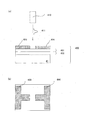
実施形態1に対応するより具体的な実施例1を説明する。本実施例に係る電磁波発生・検出装置について、図4を用いて説明する。図4(a)は、本実施例に係る電磁波発生・検出装置及び光伝導素子の構成を表す断面図である。図4(b)は、光伝導素子の構成を表す上面図である。
More specific photoconductive elements will be described in the following examples.
Example 1
A more specific example 1 corresponding to the first embodiment will be described. The electromagnetic wave generation / detection apparatus according to the present embodiment will be described with reference to FIG. FIG. 4A is a cross-sectional view illustrating configurations of the electromagnetic wave generation / detection device and the photoconductive element according to the present embodiment. FIG. 4B is a top view illustrating the configuration of the photoconductive element.
本実施例において、光伝導膜は、LT-InGaAsP層401、LT-InGaAs層402によって構成する。これらは、半絶縁性InP基板41上に結晶成長して作製する。LT-の接頭語は結晶成長の際、低温成長法を用いるという意味である。例えば、MBE(分子線エピタキシー)法を用いて250℃程度の温度で結晶成長する。LT-InGaAsP層401は1.5μmに対応するバンドギャップを持ち、LT-InGaAs層402は1.67μmに対応するバンドギャップを持つ。一例としての本実施例では、それぞれの厚さは1μmである。半導体層401上に設けた電極403、404はアンテナでもあって、本実施例では、電極403、404がダイポールアンテナの形になっている。アンテナ形状としては、ダイポールアンテナ、ボウタイアンテナなどがよく知られている。テラヘルツ波の放射パターンは、基板41にアンテナが貼り付いている形となっているため、誘電率の高い方に、つまり基板41側が大きい。
In this embodiment, the photoconductive film is composed of the LT-
本実施例の光伝導素子400の励起には、幅が数十フェムト秒の短パルス光411を発振する1.5μm帯ファイバーレーザ装置410を用いる。励起光411は、アンテナ403、404のギャップ部へ照射し、半導体層401、半導体402を順に伝搬する。LT-InGaAsP層401はそのうちの1.5μm付近を吸収し、LT-InGaAs層402はそのうちの1.67μm付近を吸収し、テラヘルツ波を発生あるいは検出する。発生用では、電極403、404の両極に不図示の電源などによって電圧をかけておくとよい。励起光411の光吸収時にピコ秒程度の寿命を持つキャリアが発生し、これが加速される。キャリアの加速は電磁界を発生する。検出用では、電極403、404の両極に不図示の電流計を接続する。検出したいテラヘルツ波電界と同時に励起光411が照射されると、励起光による光キャリアによってサンプリングされたテラヘルツ電界(実質的にはDC電界)が、電流を生成する。この電流を検出することで、テラヘルツ波が検出される。
For excitation of the
(実施例2)
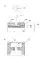
実施形態2に対応するより具体的な実施例2を説明する。本実施例に係る電磁波発生・検出装置について、図5を用いて説明する。図5(a)は、本実施例に係る電磁波発生・検出装置及び光伝導素子の構成を表す断面図である。図5(b)は、光伝導素子の構成を表す上面図である。
(Example 2)
A more specific example 2 corresponding to the second embodiment will be described. The electromagnetic wave generation / detection apparatus according to the present embodiment will be described with reference to FIG. FIG. 5A is a cross-sectional view illustrating configurations of the electromagnetic wave generation / detection device and the photoconductive element according to the present embodiment. FIG. 5B is a top view illustrating the configuration of the photoconductive element.
本実施例において、光伝導膜は、LT-InGaAs/InAlAs半導体超格子層501、502によって構成する。これらは、半絶縁性InP基板51上に結晶成長して作製する。半導体超格子層501は量子井戸6nm/トンネル障壁9nmの50周期の繰り返し、半導体超格子層502は量子井戸12nm/トンネル障壁8nmの50周期の繰り返しによって構成する。これにより、半導体超格子層501における巨視的な抵抗率(R101相当)が半導体超格子層502における巨視的な抵抗率(R102相当)より大きい光伝導膜を形成する。これらは、励起光スペクトルにおける短波長側と、これより0.2eV程度長波長側とをそれぞれ光吸収する。LT-InGaAsは、ベリリウム(Be)を不純物ドープしておいてもよい。Beはn型キャリアを補償するためのドーピングとなるため、適切にドープ濃度をコントロールすると(通常、1015〜1018cm-3)、LT-InGaAs自身の抵抗率を高くすることができる。
In this embodiment, the photoconductive film is composed of LT-InGaAs / InAlAs semiconductor superlattice layers 501 and 502. These are produced by crystal growth on a
本実施例では、介在させた絶縁膜506に開けたコンタクトホール507の部分でだけ、電極503、504が半導体層501と接している。コンタクトホールの直径ないし辺の長さは、アンテナ503、504のギャップ部の間隔dと半導体膜502の厚さtの関数として2t2/d程度が好ましい。本実施例の光伝導素子では、ギャップ部の間隔5μm、コンタクトホール径1μmを用いる。こうすることにより、容易に上述の抵抗Rvを大きく設計し、R101と(R102+2Rv)の値を同じオーダーとすることができる。
In this embodiment, the
本実施例の光伝導素子500の励起にも、実施例1と同様の短パルス光411を発振する1.5μm帯ファイバーレーザ装置410を用いる。テラヘルツ波の発生・検出方法も実施例1と同様である。
The 1.5 μm band
(実施例3)
図6は、実施例3に係る電磁波発生装置を用いたテラヘルツ時間領域分光システム(THz−TDS)を示す。この様な分光システム自体は、従来から知られているものと基本的に同じである。この分光システムは、励起光を照射するための光照射手段を成す短パルスレーザ410と、ハーフミラー610と、光遅延系620と、光伝導素子(電磁波発生素子)600と、光伝導素子(電磁波検出素子)640とを主要な要素として備える。本実施例において、電磁波発生・検出素子600、640としては、1.5μm帯に対応した実施例1の光伝導素子400を用いてもよい。ポンプ光611(超短パルス光411)、プローブ光612は、それぞれ電磁波発生素子600と電磁波検出素子640を照射する。電圧源630で電圧が印加されている電磁波発生素子600から発生したテラヘルツ波は、テラヘルツガイド613、615によって検体650に導かれる。検体650の吸収スペクトルなどの情報を含むテラヘルツ波は、テラヘルツガイド614、616によって導かれて電磁波検出素子640で検出される。このとき、電流計660の検出電流の値は、テラヘルツ波の振幅に比例する。時間分解を行う(つまり電磁波の時間波形を取得する)には、プローブ光612側の光路長を変化させる光遅延系620を動かすなど、ポンプ光とプローブ光との照射タイミングを制御すればよい。すなわち、電磁波発生素子600における電磁波発生時と電磁波検出素子660における電磁波検出時との間の遅延時間を調整する。この様に、ここでの時間領域分光装置は、電磁波発生素子を含む電磁波発生装置と、電磁波検出素子を含む電磁波検出装置と、電磁波発生装置と電磁波検出装置における電磁波発生時と電磁波検出時との間の遅延時間を調整するための調整手段を少なくとも備える。そして、調整手段により遅延時間を調整することで、発生している電磁波の時間波形をサンプリングの原理により取得する。本構成において、電磁波発生装置と電磁波検出装置の少なくとも一方を、本発明による電磁波発生・検出装置を用いて構成することができる。
(Example 3)
FIG. 6 illustrates a terahertz time domain spectroscopy system (THz-TDS) using the electromagnetic wave generation device according to the third embodiment. Such a spectroscopic system itself is basically the same as that conventionally known. This spectroscopic system includes a
101・・・半導体層(光吸収波長が短い高抵抗率の半導体層)、102・・・半導体層(光吸収波長が長い低抵抗率の半導体層)、103、104・・・複数の電極
DESCRIPTION OF
Claims (8)
光が照射された際に抵抗率が変化することにより電磁波を発生・検出し得る半導体層を有する光伝導層と、
前記半導体層と接して配された複数の電極を備え、
前記半導体層は、
抵抗率が、前記電極が接する前記半導体層の面と交わる方向に変化し、且つ、
前記半導体層において第1の領域及び前記第1の領域より前記交わる方向に前記電極から離れた第2の領域をとるとき、前記第1の領域での抵抗率が前記第2の領域での抵抗率より大きいことを特徴とする光伝導素子。 A photoconductive element that can generate and detect electromagnetic waves when irradiated with light,
A photoconductive layer having a semiconductor layer capable of generating and detecting electromagnetic waves by changing the resistivity when irradiated with light; and
Comprising a plurality of electrodes arranged in contact with the semiconductor layer;
The semiconductor layer is
The resistivity changes in a direction intersecting the surface of the semiconductor layer with which the electrode is in contact; and
In the semiconductor layer, when the first region and the second region separated from the electrode in the intersecting direction from the first region are taken, the resistivity in the first region is the resistance in the second region. A photoconductive element characterized by being greater than the rate.
前記電磁波発生装置と前記電磁波検出装置の少なくとも一方を、請求項7に記載の電磁波発生・検出装置を用いて構成したことを特徴とする時間領域分光装置。 An electromagnetic wave generator, an electromagnetic wave detector, and at least adjusting means for adjusting a delay time between the time of electromagnetic wave generation and the time of electromagnetic wave detection in the electromagnetic wave generator and the electromagnetic wave detector. Is a time domain spectroscopic device that samples and acquires the time waveform of the generated electromagnetic wave,
A time domain spectroscopic device comprising at least one of the electromagnetic wave generator and the electromagnetic wave detector using the electromagnetic wave generator / detector according to claim 7.
Priority Applications (1)
| Application Number | Priority Date | Filing Date | Title |
|---|---|---|---|
| JP2012048692A JP2012212870A (en) | 2011-03-18 | 2012-03-06 | Photoconductive element |
Applications Claiming Priority (3)
| Application Number | Priority Date | Filing Date | Title |
|---|---|---|---|
| JP2011061440 | 2011-03-18 | ||
| JP2011061440 | 2011-03-18 | ||
| JP2012048692A JP2012212870A (en) | 2011-03-18 | 2012-03-06 | Photoconductive element |
Publications (2)
| Publication Number | Publication Date |
|---|---|
| JP2012212870A true JP2012212870A (en) | 2012-11-01 |
| JP2012212870A5 JP2012212870A5 (en) | 2015-04-16 |
Family
ID=46828197
Family Applications (1)
| Application Number | Title | Priority Date | Filing Date |
|---|---|---|---|
| JP2012048692A Abandoned JP2012212870A (en) | 2011-03-18 | 2012-03-06 | Photoconductive element |
Country Status (2)
| Country | Link |
|---|---|
| US (1) | US20120236307A1 (en) |
| JP (1) | JP2012212870A (en) |
Cited By (1)
| Publication number | Priority date | Publication date | Assignee | Title |
|---|---|---|---|---|
| JP2015142101A (en) * | 2014-01-30 | 2015-08-03 | セイコーエプソン株式会社 | Photoconductivity antenna, camera, imaging apparatus, and measuring device |
Families Citing this family (3)
| Publication number | Priority date | Publication date | Assignee | Title |
|---|---|---|---|---|
| JP2015148541A (en) * | 2014-02-07 | 2015-08-20 | セイコーエプソン株式会社 | Light conduction antenna, camera, imaging apparatus and measurement apparatus |
| WO2018009517A1 (en) * | 2016-07-05 | 2018-01-11 | Massachusetts Institute Of Technology | Systems and methods for quality control of a periodic structure |
| CN107819058B (en) * | 2017-11-28 | 2019-07-23 | 厦门三安光电有限公司 | Light emitting diode |
Citations (3)
| Publication number | Priority date | Publication date | Assignee | Title |
|---|---|---|---|---|
| JPS6041215A (en) * | 1983-03-11 | 1985-03-04 | エクソン リサ−チ アンド エンジニアリング カンパニ− | Amorphous semiconductor or multilayer material containing insulator material |
| US5051804A (en) * | 1989-12-01 | 1991-09-24 | The United States Of America As Represented By The United States Department Of Energy | Photodetector having high speed and sensitivity |
| JP2006086227A (en) * | 2004-09-14 | 2006-03-30 | Osaka Univ | Optical switch |
Family Cites Families (3)
| Publication number | Priority date | Publication date | Assignee | Title |
|---|---|---|---|---|
| CA2127596C (en) * | 1993-07-16 | 2003-12-02 | Hui Chun Liu | Multicolour voltage tunable quantum well intersubband infrared photodetector and associated method |
| KR101321280B1 (en) * | 2004-12-07 | 2013-10-25 | 피코메트릭스 엘엘씨 | Photoconductive device |
| US7605371B2 (en) * | 2005-03-01 | 2009-10-20 | Osaka University | High-resolution high-speed terahertz spectrometer |
-
2012
- 2012-03-06 JP JP2012048692A patent/JP2012212870A/en not_active Abandoned
- 2012-03-09 US US13/416,421 patent/US20120236307A1/en not_active Abandoned
Patent Citations (3)
| Publication number | Priority date | Publication date | Assignee | Title |
|---|---|---|---|---|
| JPS6041215A (en) * | 1983-03-11 | 1985-03-04 | エクソン リサ−チ アンド エンジニアリング カンパニ− | Amorphous semiconductor or multilayer material containing insulator material |
| US5051804A (en) * | 1989-12-01 | 1991-09-24 | The United States Of America As Represented By The United States Department Of Energy | Photodetector having high speed and sensitivity |
| JP2006086227A (en) * | 2004-09-14 | 2006-03-30 | Osaka Univ | Optical switch |
Cited By (1)
| Publication number | Priority date | Publication date | Assignee | Title |
|---|---|---|---|---|
| JP2015142101A (en) * | 2014-01-30 | 2015-08-03 | セイコーエプソン株式会社 | Photoconductivity antenna, camera, imaging apparatus, and measuring device |
Also Published As
| Publication number | Publication date |
|---|---|
| US20120236307A1 (en) | 2012-09-20 |
Similar Documents
| Publication | Publication Date | Title |
|---|---|---|
| Burford et al. | Review of terahertz photoconductive antenna technology | |
| Yachmenev et al. | Arsenides-and related III-V materials-based multilayered structures for terahertz applications: Various designs and growth technology | |
| JP5270585B2 (en) | High speed photoconductor | |
| JP6062640B2 (en) | Photoconductive element | |
| JP5582822B2 (en) | Electromagnetic wave generator | |
| JP5656428B2 (en) | Photoconductive element | |
| JP5654760B2 (en) | Optical element | |
| Bacon et al. | Photoconductive emitters for pulsed terahertz generation | |
| JP6332980B2 (en) | Photoconductive element, photoconductive element manufacturing method, and terahertz time domain spectroscopic device | |
| US8481939B2 (en) | Photoconductive device, and terahertz wave generation and detection apparatuses each using the photoconductive device | |
| JP2012212870A (en) | Photoconductive element | |
| JP2015533023A (en) | Photomixer and manufacturing method thereof | |
| JP2012212870A5 (en) | ||
| Richter et al. | Ultrafast THz conductivity dynamics of a novel Fe-doped InGaAs quantum photoconductor | |
| Alfihed et al. | Broadband terahertz emission from photoconductive devices | |
| Minami et al. | Terahertz wave emission with 1.5 μm pump from photoconductive antenna using stacked Er-doped-InAs quantum dot layers with ultrafast carrier relaxation | |
| Dietz | Photoconductive THz emitters and detectors on the basis of InGaAs/InP for terahertz time domain spectroscopy | |
| Sun et al. | Ion-beam modified terahertz GaAs photoconductive antenna | |
| KR102230001B1 (en) | Large caliber array type terahertz wave generating device having photonic crystal structure | |
| Minot et al. | Perpendicular transport studies in GaAsAlAs superlattices by a time-resolved photocurrent experiment | |
| Cho et al. | Time-resolved study of coherent and incoherent transport in an InGaAsP/InGaAsP superlattice electro-optic modulator | |
| Singh et al. | Highly Efficient and Electrically Robust Carbon Irradiated SI-GaAs Based Photoconductive THz Emitters | |
| JP2012146758A (en) | Terahertz-wave device | |
| WO2012110759A1 (en) | Terahertz source with quantum dot material | |
| Taşyürek et al. | Intervalley scattering and field screening in germanium/silicon-germanium quantum wells |
Legal Events
| Date | Code | Title | Description |
|---|---|---|---|
| A521 | Request for written amendment filed |
Free format text: JAPANESE INTERMEDIATE CODE: A523 Effective date: 20150227 |
|
| A621 | Written request for application examination |
Free format text: JAPANESE INTERMEDIATE CODE: A621 Effective date: 20150227 |
|
| A977 | Report on retrieval |
Free format text: JAPANESE INTERMEDIATE CODE: A971007 Effective date: 20151224 |
|
| A131 | Notification of reasons for refusal |
Free format text: JAPANESE INTERMEDIATE CODE: A131 Effective date: 20160107 |
|
| A762 | Written abandonment of application |
Free format text: JAPANESE INTERMEDIATE CODE: A762 Effective date: 20160215 |