JP2012209036A - Light source device - Google Patents
Light source device Download PDFInfo
- Publication number
- JP2012209036A JP2012209036A JP2011072053A JP2011072053A JP2012209036A JP 2012209036 A JP2012209036 A JP 2012209036A JP 2011072053 A JP2011072053 A JP 2011072053A JP 2011072053 A JP2011072053 A JP 2011072053A JP 2012209036 A JP2012209036 A JP 2012209036A
- Authority
- JP
- Japan
- Prior art keywords
- light
- film
- phosphor film
- source device
- secondary light
- Prior art date
- Legal status (The legal status is an assumption and is not a legal conclusion. Google has not performed a legal analysis and makes no representation as to the accuracy of the status listed.)
- Pending
Links
Images


Classifications
-
- H—ELECTRICITY
- H01—ELECTRIC ELEMENTS
- H01L—SEMICONDUCTOR DEVICES NOT COVERED BY CLASS H10
- H01L33/00—Semiconductor devices with at least one potential-jump barrier or surface barrier specially adapted for light emission; Processes or apparatus specially adapted for the manufacture or treatment thereof or of parts thereof; Details thereof
- H01L33/48—Semiconductor devices with at least one potential-jump barrier or surface barrier specially adapted for light emission; Processes or apparatus specially adapted for the manufacture or treatment thereof or of parts thereof; Details thereof characterised by the semiconductor body packages
- H01L33/50—Wavelength conversion elements
- H01L33/507—Wavelength conversion elements the elements being in intimate contact with parts other than the semiconductor body or integrated with parts other than the semiconductor body
-
- G—PHYSICS
- G03—PHOTOGRAPHY; CINEMATOGRAPHY; ANALOGOUS TECHNIQUES USING WAVES OTHER THAN OPTICAL WAVES; ELECTROGRAPHY; HOLOGRAPHY
- G03B—APPARATUS OR ARRANGEMENTS FOR TAKING PHOTOGRAPHS OR FOR PROJECTING OR VIEWING THEM; APPARATUS OR ARRANGEMENTS EMPLOYING ANALOGOUS TECHNIQUES USING WAVES OTHER THAN OPTICAL WAVES; ACCESSORIES THEREFOR
- G03B21/00—Projectors or projection-type viewers; Accessories therefor
- G03B21/14—Details
- G03B21/20—Lamp housings
- G03B21/2006—Lamp housings characterised by the light source
- G03B21/2033—LED or laser light sources
- G03B21/204—LED or laser light sources using secondary light emission, e.g. luminescence or fluorescence
-
- H—ELECTRICITY
- H01—ELECTRIC ELEMENTS
- H01L—SEMICONDUCTOR DEVICES NOT COVERED BY CLASS H10
- H01L33/00—Semiconductor devices with at least one potential-jump barrier or surface barrier specially adapted for light emission; Processes or apparatus specially adapted for the manufacture or treatment thereof or of parts thereof; Details thereof
- H01L33/48—Semiconductor devices with at least one potential-jump barrier or surface barrier specially adapted for light emission; Processes or apparatus specially adapted for the manufacture or treatment thereof or of parts thereof; Details thereof characterised by the semiconductor body packages
- H01L33/58—Optical field-shaping elements
Abstract
Description
本発明は、投射表示装置(プロジェクタ)等の光源として使用される光源装置に関する。 The present invention relates to a light source device used as a light source for a projection display device (projector) or the like.
従来、プロジェクタ用の光源としては、超高圧水銀灯、キセノンランプ及びハロゲンランプ等の放電ランプが多く使われている。このような放電ランプに替わり、低消費電力、瞬時点灯、長寿命、高色純度及び水銀フリー等のような理由から半導体光源が提案されている。半導体光源のなかでも発光ダイオード(LED)は、近年急速に広がり、家庭用電球を従来の白熱灯からLEDへと住み替えが進められている。一方でプロジェクタ用の光源としては、一部の低輝度プロジェクタ用の光源としての採用に留まっている状況である。その理由として、LEDは面発光光源であるため、高輝度化には投入電力と面積の双方を大きくすることが必要である。言い換えれば単位面積当たりの光束量では、プロジェクタ用の光源として従来の放電ランプに替わる十分な明るさを得られていないのが実情である。 Conventionally, as a light source for a projector, a discharge lamp such as an ultra-high pressure mercury lamp, a xenon lamp, or a halogen lamp has been often used. Instead of such a discharge lamp, a semiconductor light source has been proposed for reasons such as low power consumption, instantaneous lighting, long life, high color purity and mercury-free. Among semiconductor light sources, light emitting diodes (LEDs) have spread rapidly in recent years, and household light bulbs are being replaced from conventional incandescent lamps to LEDs. On the other hand, as a light source for projectors, it has been used only as a light source for some low-intensity projectors. The reason is that since the LED is a surface emitting light source, it is necessary to increase both the input power and the area in order to increase the luminance. In other words, with the amount of light flux per unit area, the actual situation is that sufficient brightness to replace a conventional discharge lamp as a light source for a projector cannot be obtained.
そこで、不足しているLEDの光学利用効率の高効率化が提案されている(例えば、特許文献1参照。)。特許文献1では、LEDから発光した光線を楔形状のプリズムで反射させ、LEDの面積より小さい面積の射出面から出力する。これにより、光源の単位面積当たりの光束量を増加させることなく、且つ光源からの光線放射角度を小さくすることなく、発光面積と光線放射角度との関数であるエテンデューを改善し、高輝度で照明することができる。
In view of this, it has been proposed to increase the efficiency of optical utilization of the LEDs that are lacking (see, for example, Patent Document 1). In
しかしながら、特許文献1の系においては、LED自身の実質反射率は70%程度に留まり、更に正反射成分だけでなく散乱成分も多い。このため、LEDで発光した光束を自身も含めた系内で多重反射を繰り返して系外へ高効率で出力することは困難であった。
However, in the system of
上記問題点を鑑み、本発明の目的は、発光部の単位面積当たりの光束量を大きくし、光束を高効率で出力することができる光源装置を提供することである。 In view of the above problems, an object of the present invention is to provide a light source device that can increase the amount of light flux per unit area of a light emitting unit and output the light flux with high efficiency.
本発明の一態様によれば、一次光を発光する第1の固体発光素子(2、2a,31a)と、一次光を吸収し二次光を発光する第1の蛍光体膜(3,3a)と、第1の蛍光体膜(3,3a)に沿って空気を介して配置された入射面(11)と、入射面(11)と傾斜して対向する傾斜面(12)と、入射面(11)及び傾斜面(12)に垂直で互いに平行に対向する2つの垂直面(15,16)と、入射面(11)及び傾斜面(12)の間隔が広がる側で、入射面(11)、傾斜面(12)及び2つの垂直面(15,16)と連続し、第1の蛍光体膜(3,3a)の面積よりも小さい面積を有する射出面(13)と、射出面(13)と平行に対向する挟角面(14)とを有するプリズム(1)と、第1の固体発光素子(2,2a,31a)と第1の蛍光体膜(3,3a)との間に配置され、一次光を透過し且つ二次光を反射する第1の二次光反射膜(4,4a)とを備える光源装置が提供される。 According to one aspect of the present invention, the first solid-state light emitting element (2, 2a, 31a) that emits primary light and the first phosphor film (3, 3a) that absorbs primary light and emits secondary light. ), An incident surface (11) arranged via air along the first phosphor film (3, 3a), an inclined surface (12) inclined to face the incident surface (11), and incident On the side where the distance between the two vertical surfaces (15, 16) perpendicular to the surface (11) and the inclined surface (12) and parallel to each other and the incident surface (11) and the inclined surface (12) increases, the incident surface ( 11) an emission surface (13) which is continuous with the inclined surface (12) and the two vertical surfaces (15, 16) and has an area smaller than the area of the first phosphor film (3, 3a); A prism (1) having an included angle surface (14) facing in parallel with (13), a first solid state light emitting device (2, 2a, 31a) and a first Provided with a first secondary light reflecting film (4, 4a) that is disposed between the fluorescent film (3, 3a) and transmits the primary light and reflects the secondary light. .
本発明の一態様において、挟角面(14)から射出面(13)へ向かう方向において、入射面(11)の長さが、第1の蛍光体膜(3)の長さ(D1)よりも長く、第1の蛍光体膜(3)が入射面(11)の挟角面(14)側の一部と対向するように配置されており、入射面(11)の射出面(13)側の第1の蛍光体膜(3)と対向していない部分と空気を介して対向するように配置された金属膜ミラー(7)を更に備えていても良い。 In one aspect of the present invention, the length of the incident surface (11) is greater than the length (D1) of the first phosphor film (3) in the direction from the included angle surface (14) to the exit surface (13). The first phosphor film (3) is arranged so as to face a part of the incident surface (11) on the narrow-angle surface (14) side, and the exit surface (13) of the incident surface (11). You may further provide the metal film mirror (7) arrange | positioned so that the part which is not facing the 1st fluorescent substance film (3) of the side may be opposed via air.
本発明の一態様において、挟角面(14)から射出面(13)へ向かう方向において、入射面(11)の長さ及び第1の二次光反射膜(4)の長さ(D1+D2)が、第1の蛍光体膜(3)の長さ(D1)よりも長く、第1の蛍光体膜(3)が入射面(11)の挟角面(14)側の一部と対向するように配置されていても良い。 In one aspect of the present invention, the length of the incident surface (11) and the length of the first secondary light reflecting film (4) (D1 + D2) in the direction from the included angle surface (14) to the exit surface (13) Is longer than the length (D1) of the first phosphor film (3), and the first phosphor film (3) faces a part of the incident surface (11) on the narrow angle surface (14) side. It may be arranged as follows.
本発明の一態様において、傾斜面(12)に沿って空気を介して配置され、一次光を透過し且つ二次光を反射する第2の二次光反射膜(5)を更に備えていても良い。又は、傾斜面(12)に沿って空気を介して配置され、一次光及び二次光を反射する金属膜ミラーを更に備えていても良い。 In one aspect of the present invention, the apparatus further includes a second secondary light reflecting film (5) disposed along the inclined surface (12) through the air and transmitting the primary light and reflecting the secondary light. Also good. Or you may further provide the metal film mirror which is arrange | positioned through air along an inclined surface (12) and reflects primary light and secondary light.
本発明の一態様において、傾斜面(12)に沿って空気を介して配置され、一次光を吸収し二次光を発光する第2の蛍光体膜(3b)と、第2の蛍光体膜(3b)を照明するための一次光を発光する第2の固体発光素子(4b)と、第2の蛍光体膜(3b)と第2の固体発光素子(4b)との間に配置され、一次光を透過し且つ二次光を反射する第2の二次光反射膜(4b)とを更に備えていても良い。 In one aspect of the present invention, a second phosphor film (3b) that is disposed via air along the inclined surface (12) and absorbs primary light and emits secondary light, and a second phosphor film (3b) is disposed between the second solid-state light emitting element (4b) that emits primary light for illuminating the second phosphor film (3b) and the second solid-state light emitting element (4b). You may further provide the 2nd secondary light reflection film (4b) which permeate | transmits primary light and reflects secondary light.
本発明の一態様において、第1の固体発光素子(2)と第1の蛍光体膜(3)の間を囲むように配置され、一次光及び二次光を反射する内壁面を有するライトパイプ(8)を更に備えていても良い。 1 aspect of this invention WHEREIN: It is arrange | positioned so that between 1st solid light emitting element (2) and 1st fluorescent substance films (3) may be enclosed, and the light pipe which has an inner wall surface which reflects primary light and secondary light (8) may be further provided.
本発明の一態様において、ライトパイプ(8)が、第1の固体発光素子(2)側から第1の蛍光体膜(3)側に向かって広がるようにテーパ形状を有していても良い。 In one embodiment of the present invention, the light pipe (8) may have a tapered shape so as to spread from the first solid state light emitting device (2) side toward the first phosphor film (3) side. .
本発明の一態様において、射出面(13)に配置され、一次光を反射し且つ二次光を透過する一次光反射膜(6)を更に備えていても良い。 1 aspect of this invention WHEREIN: You may further provide the primary light reflection film (6) which is arrange | positioned at the output surface (13) and reflects primary light and permeate | transmits secondary light.
本発明の一態様において、第1の固体発光素子(31b)が単一波長を有する一次光を発光し、第1の二次光反射膜(4a)の分光特性が狭帯域であっても良い。 In one embodiment of the present invention, the first solid-state light emitting element (31b) may emit primary light having a single wavelength, and the spectral characteristics of the first secondary light reflecting film (4a) may be a narrow band. .
本発明によれば、発光部の単位面積当たりの光束量を大きくし、光束を高効率で出力することができる光源装置を提供することができる。 ADVANTAGE OF THE INVENTION According to this invention, the light source device which can enlarge the light beam amount per unit area of a light emission part, and can output a light beam with high efficiency can be provided.
次に、図面を参照して、本発明の第1〜第3の実施の形態を説明する。以下の図面の記載において、同一又は類似の部分には同一又は類似の符号を付している。ただし、図面は模式的なものであり、厚みと平面寸法との関係、各層の厚みの比率等は現実のものとは異なることに留意すべきである。したがって、具体的な厚みや寸法は以下の説明を参酌して判断すべきものである。又、図面相互間においても互いの寸法の関係や比率が異なる部分が含まれていることはもちろんである。 Next, first to third embodiments of the present invention will be described with reference to the drawings. In the following description of the drawings, the same or similar parts are denoted by the same or similar reference numerals. However, it should be noted that the drawings are schematic, and the relationship between the thickness and the planar dimensions, the ratio of the thickness of each layer, and the like are different from the actual ones. Therefore, specific thicknesses and dimensions should be determined in consideration of the following description. Moreover, it is a matter of course that portions having different dimensional relationships and ratios are included between the drawings.
また、以下に示す第1〜第3の実施の形態は、この発明の技術的思想を具体化するための装置や方法を例示するものであって、この発明の技術的思想は、構成部品の材質、形状、構造、配置等を下記のものに特定するものでない。この発明の技術的思想は、特許請求の範囲において、種々の変更を加えることができる。 The first to third embodiments shown below exemplify apparatuses and methods for embodying the technical idea of the present invention, and the technical idea of the present invention is the component parts. The material, shape, structure, arrangement, etc. are not specified below. The technical idea of the present invention can be variously modified within the scope of the claims.
(第1の実施の形態)
本発明の第1の実施の形態に係る光源装置は、図1に示すように、一次光(一次光源光)を発光する固体発光素子2と、一次光を吸収し二次光(二次光源光)を発光する蛍光体膜3と、蛍光体膜3と空気を介して配置された楔形状のプリズム1と、固体発光素子2と蛍光体膜3との間に配置され、固体発光素子2により発光される一次光を透過し且つ蛍光体膜3により発光される二次光を反射する第1の二次光反射膜4とを備える。
(First embodiment)
As shown in FIG. 1, the light source device according to the first embodiment of the present invention includes a solid-state
プリズム1の材料としては、屈折率が1よりも大きい硝子や樹脂が使用可能である。プリズム1の各面は表面粗さの小さい研磨面である。プリズム1は、研磨加工や切削加工のほか金型成型等により作製可能である。
As a material of the
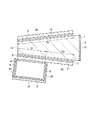
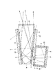
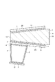
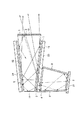
プリズム1は、図1及び図2に示すように、蛍光体膜3に沿って空気を介して配置された面(以下、「入射面」という。)11と、入射面11と傾斜して対向する面(以下、「傾斜面」という。)12と、入射面11及び傾斜面12に垂直で互いに平行に対向する2つの面(以下、「垂直面」という。)15,16と、入射面11及び傾斜面12の間隔が広がる側で、入射面11、傾斜面12及び2つの垂直面15,16と連続し、蛍光体膜3の面積よりも小さい面積を有する面(以下、「射出面」という。)13と、射出面13と平行に対向する面(以下、「挟角面」という。)14を有する。
As shown in FIGS. 1 and 2, the
図1に示した固体発光素子2としては、LEDや半導体レーザー等の種々の発光素子が使用可能である。固体発光素子2の裏面側には反射膜が形成され、発光層から発光された1次光は直接又は反射膜で反射して表面側へ射出される。固体発光素子2は、例えば上面視2mm×6mm程度の矩形を有する。本発明の第1の実施の形態においては、固体発光素子2として青色LEDを使用する。固体発光素子2は、1次光を反射する反射面を有する支持部材21により支持されている。
As the solid-state light-emitting
蛍光体膜3は、入射面11の挟角面14側の一部と対向するように、硝子等の基板23上に塗布により形成されている。蛍光体膜3の上面視における形状は固体発光素子2と略同じであり、蛍光体膜3の面積は固体発光素子2の面積と同等である。蛍光体膜3の材料としては、硫化物系、酸化物系又は窒化物系等の種々の蛍光体が採用可能である。蛍光体膜3は、二次光源として振る舞い、固体発光素子2により発光された一次光を励起光として吸収し、一次光とは異なる波長の二次光を発光する。蛍光体膜3は、例えば一次光が青色光の場合、緑色又は赤色等の紫外〜可視光を発光する。挟角面14から射出面13へ向かい入射面11に平行な方向において、基板23の長さ(D1+D2)は、蛍光体膜3の長さD1よりも長く、更に入射面11の長さは基板23の長さ(D1+D2)よりも長い。 第1の二次光反射膜4は、基板23の蛍光体膜3が配置されている面と対向する面に、蛍光体膜3と略同じ面積を有するように配置されている。第1の二次光反射膜4としては、例えば屈折率の異なる酸化ケイ素(SiO2)と酸化チタン(TiO2)からなる薄膜を交互に積層させたダイクロイック膜等が使用可能である。第1の二次光反射膜4は、基板23上に蒸着法等により形成可能である。
The
更に、基板23上の第1の二次光反射膜4が配置されていない部分には、可視光を全て高反射率(例えば98%以上)で反射する銀ミラー等の金属膜ミラー7が配置されている。金属膜ミラー7は、入射面11の射出面13側の蛍光体膜3と対向していない部分と空気を介して対向するように配置されている。
Further, a metal film mirror 7 such as a silver mirror that reflects all visible light with high reflectivity (for example, 98% or more) is disposed in a portion where the first secondary
更に、傾斜面12に沿って空気を介して第2の二次光反射膜5が配置されている。第2の二次光反射膜5は、硝子等の基板24上に配置されている。挟角面14から射出面13へ向かう傾斜面12に平行な方向において、第2の二次光反射膜5及び基板24の長さD3は、基板23の長さ(D1+D2)と略同じである。第2の二次光反射膜5は、一次光を透過し且つ二次光を反射する。第2の二次光反射膜5としては、例えば屈折率の異なる酸化ケイ素(SiO2)と酸化チタン(TiO2)からなる薄膜を交互に積層させたダイクロイック膜等が使用可能である。第2の二次光反射膜5は、基板24上に蒸着法等により形成可能である。
Furthermore, the second secondary
更に、射出面13上に一次光反射膜6が配置されている。一次光反射膜6は、一次光を反射し且つ二次光を透過する。一次光反射膜6としては、例えば屈折率の異なる酸化ケイ素(SiO2)と酸化チタン(TiO2)からなる薄膜を交互に積層させたダイクロイック膜等が使用可能である。一次光反射膜6は、射出面13上に蒸着法等により形成可能である。
Further, the primary
更に、固体発光素子2と蛍光体膜3の間を囲むように四角柱の筒(ライトパイプ)8が配置されている。ライトパイプ8は、一次光及び二次光を反射するミラーで形成された内壁面を有する。ライトパイプ8の外側には、ライトパイプ8を取り囲むようにカバー部材22が配置されている。
Further, a quadrangular cylinder (light pipe) 8 is disposed so as to surround the solid
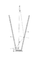
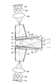
次に、本発明の第1の実施の形態に係る光源装置を用いた照明方法(光線出力の原理)を、図3〜図6を用いて説明する。なお、図3〜図6において一次光を点線矢印で示し、二次光を実線矢印で示す。 Next, an illumination method using the light source device according to the first embodiment of the present invention (principle of light output) will be described with reference to FIGS. 3 to 6, the primary light is indicated by a dotted arrow, and the secondary light is indicated by a solid arrow.
図3に示すように、固体発光素子2より発光した一次光(青色光)は、ライトパイプ8を通って第1の二次光反射膜4及び基板23を透過し、蛍光体膜3を照明する。図3及び図4に示すように、蛍光体膜3は、一次光を励起光として吸収し、二次光(緑色光)を発光する。その際、蛍光体膜3中の各蛍光体粒子のそれぞれが個々に一次光を吸収し、二次光を全方位(360度)に発光する。そのため一次光のうち約半分の光はプリズム1側に発光する。一方、残りの光はその逆側に発光するが、第1の二次光反射膜4で反射し、全ての二次光がプリズム1側に向かう。また、一次光のうちの一部が蛍光体膜3で吸収されずに蛍光体膜3を透過する。
As shown in FIG. 3, the primary light (blue light) emitted from the solid state light emitting
図5に示すように、蛍光体膜3で発光した二次光と、蛍光体膜3を透過した一部の一次光は、空気を介してプリズム1の入射面11に入射し、プリズム1内で多重反射する。プリズム1の各面は鏡面研磨されているため、屈折率の高いプリズム1から低い系外へは、スネルの法則を満たす角度以上の光線は、全て臨界角を超えてプリズム1内で内部反射を起こす。したがって、2つの垂直面15,16及び挟角面14では、蛍光体膜3から入射する全ての一次光及び二次光が内部反射する。
As shown in FIG. 5, the secondary light emitted from the
一方、入射面11及び傾斜面12では、プリズム1内に入射した際一部の光線が臨界角を越えないため、プリズム1系外に射出する。射出した光線は、第1の二次光反射膜4、第2の二次光反射膜5及び金属膜ミラー7で反射して再びプリズム1に戻される。プリズム1は、射出面13側に広がるように楔形状を有するため、臨界角を超えていない光線も、多重反射を繰り返すことで臨界角を超え、内部反射するようになる。蛍光体膜3から出力した光線が臨界角を超えて多重反射を繰り返すように、図1に示した蛍光体膜3の長さD1に対し、プリズム1の入射面11、射出面12及び2つの垂直面15,16を長くし、且つ金属膜ミラー7の長さD2及び第2の二次光反射膜5の長さD3を適宜長くしている。このようにして、プリズム1内で多重反射を繰り返すことで射出面13から高効率で光線を系外に射出する。
On the other hand, at the
また、図6に示すように、二次光が入射面11からプリズム外に射出され、第1の二次光反射膜4に入射する際、硝子と空気の屈折率差の方が硝子と蛍光体膜3の屈折率差に比べ大きいため、第1の二次光反射膜4に入射する二次光の入射角は小さくなる。そのため、二次光反射膜4は二次光を高い確率で反射することができる。
In addition, as shown in FIG. 6, when the secondary light is emitted from the
以上説明したように、本発明の第1の実施の形態に係る光源装置によれば、二次光を発光する蛍光体膜3の面積が、二次光を射出する射出面13の面積より大きいため、エテンデューを改善し、高輝度で照明することができる。そして、固体発光素子2からの一次光で蛍光体膜3が二次光を発光し、二次光を第1の二次光反射膜4で反射させることにより、入射面11及び傾斜面12同士で二次光がそれぞれ多重反射を繰り返し、射出面13から効率的に二次光を出力させることができる。よって、単位面積当たりの光束量を大きくすることができ、光束を高効率で出力することができることが可能となる。
As described above, according to the light source device according to the first embodiment of the present invention, the area of the
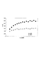
図7に蛍光体膜3の面積と明るさの関係についてのシミュレーション結果を示す。蛍光体膜3の面積、並びにプリズム1の入射面11及び傾斜面12のなす楔の角度によって詳細は異なるが、比較例としてのLEDから発光した光をそのままプリズムへ入射し、多重反射を繰り返して射出させる構成に対して、本発明の第1の実施の形態に係る光源装置では2倍近く明るくなる可能性がある。特に、蛍光体膜3の面積を大きくすることでその効果があり、従来LEDを大きくしても効果はないとされていた限界を超えることから、高輝度化が期待できる。
FIG. 7 shows a simulation result of the relationship between the area of the
更に、本発明の第1の実施の形態に係る光源装置によれば、第2の二次光反射膜5を配置することにより、傾斜面12から射出した二次光をプリズム1内に戻すことができる。
Furthermore, according to the light source device according to the first embodiment of the present invention, the secondary light reflected from the
ところで、一次光及び二次光は、図8に示すような分光特性を持っている。蛍光体膜3からプリズム1に入射する光線には、上述したように二次光のほかに一部一次光が混入している。これは、蛍光体膜3の発光効率に関わるもので、蛍光体膜3で吸収されずにそのまま透過してくる成分である。この成分が射出光に混ざっていると、所望のスペクトルが得られず純色を悪くする。図9に示すように、第1の二次光反射膜4、第2の二次光反射膜5及び一次光反射膜6は、それぞれの帯域で98%以上の高反射である。したがって、第2の二次光反射膜5を配置することにより、臨界角を超えない光線の青色光成分を、第2の二次光反射膜5を透過して系外に排出することができる。
Incidentally, the primary light and the secondary light have spectral characteristics as shown in FIG. As described above, in addition to the secondary light, the primary light is partially mixed in the light beam incident on the
更に、本発明の第1の実施の形態に係る光源装置によれば、射出面13に一次光反射膜6を配置することで、蛍光体膜3で吸収されることなく透過した一次光を射出面13から出力させることなくプリズム1内に戻すことができる。この一次光が蛍光体膜3を再び励起させ発光させることで、二次光を更に増幅し、単位面積当たりの光束量を大きくすることができる。
Furthermore, according to the light source device according to the first embodiment of the present invention, the primary
更に、固体発光素子2の表面に配置される電極、及び電極に電力供給するためのワイヤボンディングのループといった物理的な要因から、固体発光素子2とプリズム1とは離間して配置されている。本発明の第1の実施の形態に係る光源装置によれば、ライトパイプ8を有することで、固体発光素子2とプリズム1との隙間からの光束の漏れを防止することができる。
Furthermore, the solid
<変形例>
本発明の第1の実施の形態の変形例として、図10に示すように、第1の二次光反射膜4が基板23と蛍光体膜3の間に配置されていても良い。更に、第1の二次光反射膜4は、基板23全面を覆っていても良い。第1の二次光反射膜4の長さ(D1+D2)は、蛍光体膜3の長さD1よりも長い。
<Modification>
As a modification of the first embodiment of the present invention, as shown in FIG. 10, the first secondary
本発明の第1の実施の形態の変形例では、図11に示すように、蛍光体膜3が基板23側に発光した二次光は直下の第1の二次光反射膜4で反射され、全ての二次光がプリズム1側へ向かう。また、プリズム1内から入射面11を介して射出した二次光は第1の二次光反射膜4により反射されてプリズム1内に戻される。
In the modification of the first embodiment of the present invention, as shown in FIG. 11, the secondary light emitted from the
(第2の実施の形態)
本発明の第1の実施の形態では、固体発光素子2及び蛍光体膜3の1組の光源を有する場合を説明したが、本発明の第2の実施の形態では、2組の光源を有する場合を説明する。
(Second Embodiment)
In the first embodiment of the present invention, the case of having one set of light sources of the solid state
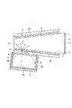
本発明の第2の実施の形態に係る光源装置は、図12に示すように、プリズム1の入射面11側に、入射面11に沿って空気を介して配置され、一次光を吸収し二次光を発光する第1の蛍光体膜3aと、第1の蛍光体膜3aを照明するための一次光を発光する第1の固体発光素子2aと、第1の蛍光体膜3aと第1の固体発光素子2aとの間に配置され、一次光を透過し且つ二次光を反射する第1の二次光反射膜4aを備える。
As shown in FIG. 12, the light source device according to the second embodiment of the present invention is disposed on the
第1の固体発光素子2aは支持部材21aにより支持されている。第1の固体発光素子2a及び第1の蛍光体膜3aの間には、ライトパイプ8a及びカバー部材22aが配置されている。
The first solid state light emitting
第1の蛍光体膜3a及び第1の二次光反射膜4aは基板23aに配置されている。基板23aの第1の蛍光体膜3aが配置されていない部分には、可視光を全て高反射率(例えば98%以上)で反射する銀ミラー等の金属膜ミラー7aが配置されている。
The
更に、本発明の第2の実施の形態に係る光源装置は、プリズム1の傾斜面12側に、傾斜面12に沿って空気を介して配置され、一次光を吸収し二次光を発光する第2の蛍光体膜3bと、第2の蛍光体膜3bを照明するための一次光を発光する第2の固体発光素子2bと、第2の蛍光体膜3bと第2の固体発光素子2bとの間に配置され、一次光を透過し且つ二次光を反射する第2の二次光反射膜4bを備える。
Furthermore, the light source device according to the second embodiment of the present invention is disposed on the
第2の固体発光素子2bは支持部材21bにより支持されている。第2の固体発光素子2b及び第2の蛍光体膜3bの間には、ライトパイプ8b及びカバー部材22bが配置されている。
The second solid state light emitting
第2の蛍光体膜3b及び第2の二次光反射膜4bは基板23bに配置されている。基板23bの第2の蛍光体膜3bが配置されていない部分には、可視光を全て高反射率(例えば98%以上)で反射する銀ミラー等の金属膜ミラー7bが配置されている。
The
他の構成は、本発明の第1の実施の形態と実質的に同様であるので、重複した説明を省略する。 Other configurations are substantially the same as those of the first embodiment of the present invention, and a duplicate description is omitted.
次に、本発明の第2の実施の形態に係る光源装置を用いた照明方法の一例を、図12を用いて説明する。 Next, an example of an illumination method using the light source device according to the second embodiment of the present invention will be described with reference to FIG.
第1の固体発光素子2aが発光した一次光は、ライトパイプ8aを介して第1の二次光反射膜4a、基板23aを透過し、第1の蛍光体膜3aを照明する。第1の蛍光体膜3aが一次光を吸収して二次光を発光する。一方、第2の固体発光素子2bが発光した一次光は、ライトパイプ8bを介して第2の二次光反射膜4b、基板23bを透過し、第2の蛍光体膜3bを照明する。第2の蛍光体膜3bが、一次光を吸収して二次光を発光する。
The primary light emitted from the first solid state light emitting
第1の蛍光体膜3a及び第2の蛍光体膜3bのそれぞれからの二次光は、第1の二次光反射膜4a及び第2の二次光反射膜4bで反射した二次光及び一次光の残光成分と共に空気を介してプリズム1に入射し、プリズム1内及びプリズム1近傍の第1の二次光反射膜4a、第2の二次光反射膜4b、金属膜ミラー7a,7bで多重反射を繰り返し、射出面13から出力する。
The secondary light from each of the
このとき、第1の蛍光体膜3a及び第2の蛍光体膜3bで発光した一部の二次光は、相対する面の第1の蛍光体膜3a及び第2の蛍光体膜3bにそれぞれ入射する。第1の蛍光体膜3a及び第2の蛍光体膜3bは、一次光に対しては吸収特性を示すが、二次光に対しては吸収特性を持たないため、二次光は第1の蛍光体膜3a及び第2の蛍光体膜3bをそれぞれ透過又は一部散乱し、第1の二次光反射膜4a及び第2の二次光反射膜4bにより反射し、再び第1の蛍光体膜3a及び第2の蛍光体膜3bを透過してプリズム1に再入射する。一方、一次光の残留成分の一部も同様に相対する面の第1の蛍光体膜3a及び第2の蛍光体膜3bに入射するが、第1の蛍光体膜3a及び第2の蛍光体膜3bが吸収して二次光の発光に寄与する。
At this time, some secondary lights emitted from the
また、一部の一次光は、射出面13において一次光反射膜6で反射し再び系内に戻される。一次光に関しては完全に閉ざされた系を呈しているので、再び多重反射を繰り返し、第1の蛍光体膜3a及び第2の蛍光体膜3bに再度入射し吸収され発光に寄与する。第1の蛍光体膜3a及び第2の蛍光体膜3bを再度透過した一次光は、第1の二次光反射膜4a及び第2の二次光反射膜4bと基板23a,23bを透過して、ライトパイプ8a,8bを介して第1の固体発光素子2a及び第2の固体発光素子2bに戻る。この光線は、第1の固体発光素子2a及び第2の固体発光素子2b自身で反射し、再度第1の蛍光体膜3a及び第2の蛍光体膜3bを照明する。このように残留成分も含めて、全ての一次光が第1の蛍光体膜3a及び第2の蛍光体膜3bで吸収され二次光の発光に寄与する。
Further, a part of the primary light is reflected by the primary
以上説明したように、本発明の第2の実施の形態に係る光源装置によれば、複数の光源を合成するような系においても、単位面積当たりの光束量が大きく、且つ高効率で照明可能となる。 As described above, according to the light source device according to the second embodiment of the present invention, even in a system in which a plurality of light sources are combined, the amount of light flux per unit area is large and illumination can be performed with high efficiency. It becomes.
(第3の実施の形態)
本発明の第3の実施の形態に係る光源装置は、図13に示すように、ライトパイプ8が固体発光素子2側から蛍光体膜3側へ向かって広がるようにテーパ形状を有する点が、本発明の第1の実施の形態と異なる。蛍光体膜3及び第1の二次光反射膜4の面積は、固体発光素子2の面積よりも大きい。他の構成は、本発明の第1の実施の形態と実質的に同様であるので、重複した説明を省略する。
(Third embodiment)
As shown in FIG. 13, the light source device according to the third embodiment of the present invention has a tapered shape so that the
次に、本発明の実施の形態に係る光源装置を用いた照明方法の一例を、図14及び図15を用いて説明する。 Next, an example of an illumination method using the light source device according to the embodiment of the present invention will be described with reference to FIGS.
図14に示すように、固体発光素子2より発光した一次光は、固体発光素子2の表面の法線方向に対し角度θ0を有しており、ライトパイプ8内で多重反射しながら射出面13へ向かう。この時、ライトパイプ8内の反射面が傾斜しているため、一次光が反射するたびに、蛍光体膜3へ向かう角度θ0,θ1,θ2が小さくなる。したがって、ライトパイプ8から射出する一次光はいずれも略平行光となる。ライトパイプ8を射出した1次光は基板23を透過し、第1の二次光反射膜4を透過し蛍光体膜3を照明する。
As shown in FIG. 14, the primary light emitted from the solid state light emitting
ここで、図15に示すように、第1の二次光反射膜4を構成するダイクロイックミラーの角度特性において、入射する光線の角度が大きくなると、分光反射特性が短波長側にシフトする。そのため一次光であっても光線角度が大きい成分を透過できず、一次光で十分に蛍光体膜3を照明できない現象が発生し、所望の高輝度化が得られない場合がある。これに対して、本発明の第3の実施の形態によれば、ライトパイプ8がテーパ形状を有することにより、一次光を略平行光とすることができるので、第1の二次光反射膜4の角度特性で反射されることなく高効率で蛍光体膜3を照明することができる。
Here, as shown in FIG. 15, in the angle characteristics of the dichroic mirror constituting the first secondary
そして、照明された蛍光体膜3は、1次光を吸収し二次光(緑色光)を発光する。その際、蛍光体膜3内部の各蛍光体粒子それぞれが個々に青色光を吸収し、緑色光を全方位(360度)に発光する。そのため一次光の約半分の光はプリズム1側に発光するが、残りの光はその逆の基板23側に発光する。今度はかなり角度のついた光線が第1の二次光反射膜4に入射するが、第1の二次光反射膜4の角度特性により、二次光の反射帯域は広がるため、略全ての光を反射し、プリズム1側に向けることができる。そして、図16に示すように、蛍光体膜3により発光された二次光がプリズム1、第1の二次光反射膜4、第2のニ次反射膜5及び金属膜ミラー7により多重反射を繰り返し、射出面13から射出される。このとき、ライトパイプ8がテーパ形状を有することにより、ライトパイプ8の径が一定の場合と比して、ライトパイプ8に再入射した光線をプリズム1に戻しやすくなる。
The illuminated
以上説明したように、本発明の第3の実施の形態に係る光源装置によれば、テーパ形状のライトパイプ8を備えることにより、高効率で蛍光体膜3を照明でき、蛍光体膜3発光の高輝度化により、射出される光束の単位面積当たりの光束量を大きくすることができる。 更に、プリズム1内で多重反射し、再び蛍光体膜3に戻ってくる一次光が所定の入射角以上で入射する場合には、第1の二次光反射膜4を透過することなく、再び蛍光体膜3へ戻すことができる。よって、一次光を高効率で蛍光体膜3を照明することができる。
As described above, according to the light source device according to the third embodiment of the present invention, by providing the tapered
<第1の変形例>
本発明の第3の実施の形態の第1の変形例として、図17に示すように、2組の光源を有し、ライトパイプ8a,8bのそれぞれが、第1の固体発光素子2a及び第2の固体発光素子2bから第1の蛍光体膜3a及び第2の蛍光体膜3bに向かってテーパ形状を有していても良い。他の構成は、図12に示した本発明の第2の実施の形態に係る光源装置と実質的に同様であるので、重複した説明を省略する。
<First Modification>
As a first modified example of the third embodiment of the present invention, as shown in FIG. 17, two sets of light sources are provided, and each of the
<第2の変形例>
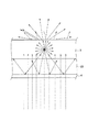
本発明の第3の実施の形態の第2の変形例として、図18に示すように、LEDの代わりに、単一波長を出力するレーザー31a,31bを使用しても良い。レーザー31a,31bは、系外に配置されている。図18にはレーザー31a,31bのそれぞれが複数個使いのレーザーアレイを示すが、レーザー31a,31bのそれぞれは1個でも良く、個数は特に限定されない。レーザー31a,31bは、図19に示すような単一波長の青色レーザーを発光する。レーザー31a,31bから出力される光線は放射状に発光し、コリメートレンズ32a,32bで平行光にされる。その後、複数の平行光は共通の集光レンズ33a,33bによりライトパイプ8a,8bの端面に入射する。ライトパイプ8a,8b内を多重反射した光線は、略平行光として第1の蛍光体膜3a及び第2の蛍光体膜3bをそれぞれ照明する。他の構成は、図17に示した構成と実質的に同様であるので、重複した説明を省略する。
<Second Modification>
As a second modification of the third embodiment of the present invention, as shown in FIG. 18,
図19に示す青色レーザーのように単一波長を出力する場合、第1の二次光反射膜4a及び第2の二次光反射膜4bとして、図20に示すように、蛍光体膜3を照明する略平行光は透過し、プリズム1内多重反射で戻ってくるような戻り光を反射するような帯域の狭い反射膜を使用することで、一次光を系内に閉じ込めて、全ての一次光を蛍光体膜3での発光に寄与させることが可能となる。
When a single wavelength is output as in the blue laser shown in FIG. 19, as shown in FIG. 20, the
(その他の実施の形態)
上記のように、本発明は第1〜第3の実施の形態によって記載したが、この開示の一部をなす論述及び図面はこの発明を限定するものであると理解すべきではない。この開示から当業者には様々な代替実施の形態、実施例及び運用技術が明らかとなろう。
(Other embodiments)
As described above, the present invention has been described according to the first to third embodiments. However, it should not be understood that the description and drawings constituting a part of this disclosure limit the present invention. From this disclosure, various alternative embodiments, examples and operational techniques will be apparent to those skilled in the art.
例えば、図1に示した第2の二次光反射膜5の代わりに、可視光を全て高反射率(例えば98%以上)で反射する銀ミラー等の金属膜ミラーを備えていても良い。金属膜ミラーを配置することにより、蛍光体膜3で吸収されることなく透過した一次光をプリズム1内に戻し、蛍光体膜3を再び励起させ発光させることで、二次光を更に増幅し、単位面積当たりの光束量を大きくすることができる。
For example, instead of the second secondary
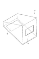
また、本発明の第1〜第3の実施の形態において、楔形状のプリズム1について説明したが、プリズム1の代わりに、図21に示すような空気が充填された楔形状の筺体1xを使用しても良い。この場合、筐体1xの内壁面には一次光及び二次光を反射する金属膜ミラー又は二次光を反射する二次光反射膜を形成する。更に、蛍光体膜3からの二次光を入射するための開口部17と、二次光を射出させるための開口部17の面積より大きい開口部18を設ければ良い。
Further, in the first to third embodiments of the present invention, the wedge-shaped
また、本発明の第1〜第3の実施の形態に係るプリズム1は、射出面13に比較して、入射面11及び傾斜面12が著しく大きな構成でも良い。また、プリズム1の射出面13に比較して、蛍光体膜3の面積が著しく大きな構成でも良い。また、プリズム1の挟角面14がなく、入射面11及び傾斜面12が連続している楔形状の場合にも適用可能である。また、垂直面15,16は、入射面11及び傾斜面12に垂直で且つ互いに平行であることが好ましいが、厳密に垂直及び平行でなくても良い。更に、射出面13及び挟角面14は、互いに平行であることが好ましいが、厳密に平行でなくても良い。
In addition, the
また、本発明の第1〜第3の実施の形態において、一次光として青色、二次光として緑色を発光させる場合を説明したが、一次光の青色光で励起して二次光として図8に示すような波長帯域の赤色光を発光することも可能である。さらに、波長の短い(エネルギーの大きい)紫外線光を励起光として、可視光域の所望のスペクトルを発光しても良い。その場合、二次光反射膜4,5,4a,4bとして、それぞれの帯域のスペクトルを反射及び透過する膜を適宜選択可能である。
In the first to third embodiments of the present invention, the case where blue light is emitted as the primary light and green light is emitted as the secondary light has been described. However, the secondary light is excited by the blue light of the primary light as shown in FIG. It is also possible to emit red light having a wavelength band as shown in FIG. Furthermore, a desired spectrum in the visible light region may be emitted using ultraviolet light having a short wavelength (high energy) as excitation light. In that case, as the secondary
また、本発明の第1〜第3の実施の形態に係る光源装置は、光源装置から射出された二次光を変調する空間光変調素子と、変調された二次光の像を結像させ、スクリーン等に表示させる結像光学系を有する画像表示装置にも適用可能である。 In addition, the light source device according to the first to third embodiments of the present invention forms a spatial light modulation element that modulates the secondary light emitted from the light source device and an image of the modulated secondary light. The present invention is also applicable to an image display apparatus having an imaging optical system that displays on a screen or the like.
このように、本発明はここでは記載していない様々な実施の形態等を含むことは勿論である。したがって、本発明の技術的範囲は上記の説明から妥当な特許請求の範囲に係る発明特定事項によってのみ定められるものである。 As described above, the present invention naturally includes various embodiments not described herein. Therefore, the technical scope of the present invention is defined only by the invention specifying matters according to the scope of claims reasonable from the above description.
1…プリズム
1x…筐体
2,2a,2b…固体発光素子
3,3a,3b…蛍光体膜
4,4a,4b,5…二次光反射膜
6…一次光反射膜
7,7a,7b…金属膜ミラー
8,8a,8b…ライトパイプ
11…入射面
12…傾斜面
13…射出面
14…挟角面
15,16…垂直面
17,18…開口部
21,21a,21b…支持部材
22,22a,22b…カバー部材
23,23a,23b,24…基板
31a,31b…レーザー
32a,32b…コリメートレンズ
33a,33b…集光レンズ
DESCRIPTION OF
Claims (10)
前記一次光を吸収し二次光を発光する第1の蛍光体膜と、
前記第1の蛍光体膜に沿って空気を介して配置された入射面と、前記入射面と傾斜して対向する傾斜面と、前記入射面及び前記傾斜面に垂直で互いに平行に対向する2つの垂直面と、前記入射面及び前記傾斜面の間隔が広がる側で、前記入射面、前記傾斜面及び前記2つの垂直面と連続し、前記第1の蛍光体膜の面積よりも小さい面積を有する射出面と、前記射出面と平行に対向する挟角面とを有するプリズムと、
前記第1の固体発光素子と前記第1の蛍光体膜との間に配置され、前記一次光を透過し且つ前記二次光を反射する第1の二次光反射膜
とを備えることを特徴とする光源装置。 A first solid state light emitting device emitting primary light;
A first phosphor film that absorbs the primary light and emits secondary light;
An incident surface disposed via air along the first phosphor film, an inclined surface that is inclined and opposed to the incident surface, and 2 that are perpendicular to the incident surface and the inclined surface and are parallel to each other. Two vertical surfaces, and a side where the interval between the incident surface and the inclined surface is widened, and is continuous with the incident surface, the inclined surface, and the two vertical surfaces, and has an area smaller than the area of the first phosphor film. A prism having an exit surface and a narrow angle surface facing in parallel with the exit surface;
A first secondary light reflecting film disposed between the first solid-state light emitting element and the first phosphor film and transmitting the primary light and reflecting the secondary light. A light source device.
前記第1の蛍光体膜が前記入射面の前記挟角面側の一部と対向するように配置されており、
前記入射面の前記射出面側の前記第1の蛍光体膜と対向していない部分と空気を介して対向するように配置された金属膜ミラーを更に備えることを特徴とする請求項1に記載の光源装置。 In the direction from the sandwiched surface to the exit surface, the length of the entrance surface is longer than the length of the first phosphor film,
The first phosphor film is disposed so as to face a part of the incident surface on the narrow surface side;
The metal film mirror further arranged so that it may oppose via the air with the part which is not facing the said 1st fluorescent substance film of the said output surface side of the said incident surface. Light source device.
前記第1の蛍光体膜が前記入射面の前記挟角面側の一部と対向するように配置されていることを特徴とする請求項1に記載の光源装置。 In the direction from the sandwiched surface to the exit surface, the lengths of the entrance surface and the first secondary light reflection film are longer than the length of the first phosphor film,
The light source device according to claim 1, wherein the first phosphor film is disposed so as to face a part of the incident surface on the narrow-angle surface side.
前記第2の蛍光体膜を照明するための前記一次光を発光する第2の固体発光素子と、
前記第2の蛍光体膜と前記第2の固体発光素子との間に配置され、前記一次光を透過し且つ前記二次光を反射する第2の二次光反射膜
とを更に備えることを特徴とする請求項1〜3のいずれか1項に記載の光源装置。 A second phosphor film disposed along the inclined surface via air, absorbing the primary light and emitting secondary light;
A second solid-state light emitting element that emits the primary light for illuminating the second phosphor film;
A second secondary light reflecting film that is disposed between the second phosphor film and the second solid state light emitting element and transmits the primary light and reflects the secondary light. The light source device according to claim 1, wherein the light source device is a light source device.
前記第1の二次光反射膜の分光特性が狭帯域であることを特徴とする請求項1〜9のいずれか1項に記載の光源装置。 The first solid state light emitting device emits the primary light having a single wavelength;
The light source device according to claim 1, wherein spectral characteristics of the first secondary light reflection film are in a narrow band.
Priority Applications (3)
| Application Number | Priority Date | Filing Date | Title |
|---|---|---|---|
| JP2011072053A JP2012209036A (en) | 2011-03-29 | 2011-03-29 | Light source device |
| PCT/JP2012/058060 WO2012133485A1 (en) | 2011-03-29 | 2012-03-28 | Light source device |
| TW101111086A TW201241544A (en) | 2011-03-29 | 2012-03-29 | Light source device |
Applications Claiming Priority (1)
| Application Number | Priority Date | Filing Date | Title |
|---|---|---|---|
| JP2011072053A JP2012209036A (en) | 2011-03-29 | 2011-03-29 | Light source device |
Publications (1)
| Publication Number | Publication Date |
|---|---|
| JP2012209036A true JP2012209036A (en) | 2012-10-25 |
Family
ID=46931194
Family Applications (1)
| Application Number | Title | Priority Date | Filing Date |
|---|---|---|---|
| JP2011072053A Pending JP2012209036A (en) | 2011-03-29 | 2011-03-29 | Light source device |
Country Status (3)
| Country | Link |
|---|---|
| JP (1) | JP2012209036A (en) |
| TW (1) | TW201241544A (en) |
| WO (1) | WO2012133485A1 (en) |
Cited By (5)
| Publication number | Priority date | Publication date | Assignee | Title |
|---|---|---|---|---|
| JP2014089235A (en) * | 2012-10-29 | 2014-05-15 | Ushio Inc | Light source device and projector |
| WO2014156550A1 (en) * | 2013-03-28 | 2014-10-02 | ウシオ電機株式会社 | Fluorescent light source device |
| CN104570563A (en) * | 2015-01-06 | 2015-04-29 | 深圳雅图数字视频技术有限公司 | Projector, projector shell and buckle structure thereof |
| US10423055B2 (en) | 2015-02-20 | 2019-09-24 | Ricoh Company, Ltd. | Illumination device and image projection apparatus |
| CN112540498A (en) * | 2019-09-20 | 2021-03-23 | 精工爱普生株式会社 | Wavelength conversion element, light source device, and projector |
Families Citing this family (5)
| Publication number | Priority date | Publication date | Assignee | Title |
|---|---|---|---|---|
| CN106569380B (en) * | 2015-10-08 | 2019-04-16 | 台达电子工业股份有限公司 | Light feeding mechanism and optical projection system |
| CN106814528B (en) * | 2015-11-27 | 2018-10-02 | 中强光电股份有限公司 | Projection arrangement and its lighting system |
| CN105487331B (en) * | 2016-01-14 | 2017-12-08 | 张建平 | A kind of light source assembly for optical projection system |
| CN107062001B (en) * | 2016-12-22 | 2023-04-07 | 毅丰显示科技(深圳)有限公司 | Light emitting diode array light source |
| CN115976868A (en) | 2018-05-28 | 2023-04-18 | 皮尔森生物工程技术(北京)有限公司 | Efficient methods and compositions for recovering products from organic acid pretreatment of plant material |
Citations (7)
| Publication number | Priority date | Publication date | Assignee | Title |
|---|---|---|---|---|
| JP2000231344A (en) * | 1999-02-10 | 2000-08-22 | Toshiba Corp | Illuminator for projection type display device |
| JP2006171207A (en) * | 2004-12-14 | 2006-06-29 | Casio Comput Co Ltd | Light source unit and projector device |
| JP2008009075A (en) * | 2006-06-28 | 2008-01-17 | Sony Corp | Light pipe, liquid crystal display |
| JP2009521786A (en) * | 2005-12-23 | 2009-06-04 | スリーエム イノベイティブ プロパティズ カンパニー | LED-based multicolor polarized illumination light source |
| JP2009150938A (en) * | 2007-12-18 | 2009-07-09 | Casio Comput Co Ltd | Light source device and projector |
| JP2009175691A (en) * | 2007-12-26 | 2009-08-06 | Victor Co Of Japan Ltd | Light source device, lighting device and image display device |
| JP2011521547A (en) * | 2008-05-06 | 2011-07-21 | クゥアルコム・インコーポレイテッド | AGC for slicer based low power demodulator |
Family Cites Families (1)
| Publication number | Priority date | Publication date | Assignee | Title |
|---|---|---|---|---|
| KR20100103697A (en) * | 2008-01-17 | 2010-09-27 | 웨이비엔, 인코포레이티드 | Light multiplexer and recycler, and micro-projector incorporating the same |
-
2011
- 2011-03-29 JP JP2011072053A patent/JP2012209036A/en active Pending
-
2012
- 2012-03-28 WO PCT/JP2012/058060 patent/WO2012133485A1/en active Application Filing
- 2012-03-29 TW TW101111086A patent/TW201241544A/en unknown
Patent Citations (7)
| Publication number | Priority date | Publication date | Assignee | Title |
|---|---|---|---|---|
| JP2000231344A (en) * | 1999-02-10 | 2000-08-22 | Toshiba Corp | Illuminator for projection type display device |
| JP2006171207A (en) * | 2004-12-14 | 2006-06-29 | Casio Comput Co Ltd | Light source unit and projector device |
| JP2009521786A (en) * | 2005-12-23 | 2009-06-04 | スリーエム イノベイティブ プロパティズ カンパニー | LED-based multicolor polarized illumination light source |
| JP2008009075A (en) * | 2006-06-28 | 2008-01-17 | Sony Corp | Light pipe, liquid crystal display |
| JP2009150938A (en) * | 2007-12-18 | 2009-07-09 | Casio Comput Co Ltd | Light source device and projector |
| JP2009175691A (en) * | 2007-12-26 | 2009-08-06 | Victor Co Of Japan Ltd | Light source device, lighting device and image display device |
| JP2011521547A (en) * | 2008-05-06 | 2011-07-21 | クゥアルコム・インコーポレイテッド | AGC for slicer based low power demodulator |
Cited By (8)
| Publication number | Priority date | Publication date | Assignee | Title |
|---|---|---|---|---|
| JP2014089235A (en) * | 2012-10-29 | 2014-05-15 | Ushio Inc | Light source device and projector |
| WO2014156550A1 (en) * | 2013-03-28 | 2014-10-02 | ウシオ電機株式会社 | Fluorescent light source device |
| JP2014192127A (en) * | 2013-03-28 | 2014-10-06 | Ushio Inc | Fluorescent light source device |
| CN104570563A (en) * | 2015-01-06 | 2015-04-29 | 深圳雅图数字视频技术有限公司 | Projector, projector shell and buckle structure thereof |
| CN104570563B (en) * | 2015-01-06 | 2016-08-24 | 深圳雅图数字视频技术有限公司 | Scialyscope, projector housing and buckle structure thereof |
| US10423055B2 (en) | 2015-02-20 | 2019-09-24 | Ricoh Company, Ltd. | Illumination device and image projection apparatus |
| CN112540498A (en) * | 2019-09-20 | 2021-03-23 | 精工爱普生株式会社 | Wavelength conversion element, light source device, and projector |
| CN112540498B (en) * | 2019-09-20 | 2022-08-23 | 精工爱普生株式会社 | Wavelength conversion element, light source device, and projector |
Also Published As
| Publication number | Publication date |
|---|---|
| TW201241544A (en) | 2012-10-16 |
| WO2012133485A1 (en) | 2012-10-04 |
Similar Documents
| Publication | Publication Date | Title |
|---|---|---|
| WO2012133485A1 (en) | Light source device | |
| US11035528B2 (en) | Light emitting device with diffuser and light reflector and projection system having the same | |
| KR101995543B1 (en) | Light Source System and Projection Device | |
| JP5671666B2 (en) | Solid light source device and projection display device | |
| US20180080627A1 (en) | Light sources system and projection device using the same | |
| JP4757974B2 (en) | Light source for projection display | |
| CN107515511B (en) | Light source system and projection equipment | |
| JP5605047B2 (en) | Light source device and projection display device using the same | |
| US20130107226A1 (en) | Projection system comprising a solid state light source and a luminsecent material | |
| JP6323020B2 (en) | Light source device and projector | |
| US20140022512A1 (en) | Phosphor-based lamps for projection display | |
| US20130194551A1 (en) | Illumination device, projecting device and lighting device | |
| US10324247B2 (en) | Optical device for producing high brightness light | |
| TWM552112U (en) | Light source device and projection system | |
| CN108693690B (en) | Light source device and projector | |
| JP2012141411A (en) | Light source device | |
| JP2013102078A (en) | Light source device and luminaire | |
| JP6926589B2 (en) | Light source device and projector | |
| JP2011118187A (en) | Light deflection element, light source apparatus and display apparatus | |
| JP2019528482A (en) | Laser LED hybrid light source for projection display | |
| US11175573B2 (en) | Light source device and projector | |
| JP2011138627A (en) | Light source device | |
| JP2015194605A (en) | Illumination device and projector | |
| CN106950785B (en) | Light source device and lighting device | |
| JP6835059B2 (en) | Light source device and projector |
Legal Events
| Date | Code | Title | Description |
|---|---|---|---|
| A621 | Written request for application examination |
Free format text: JAPANESE INTERMEDIATE CODE: A621 Effective date: 20131001 |
|
| A131 | Notification of reasons for refusal |
Free format text: JAPANESE INTERMEDIATE CODE: A131 Effective date: 20140610 |
|
| A02 | Decision of refusal |
Free format text: JAPANESE INTERMEDIATE CODE: A02 Effective date: 20141111 |