JP2012208066A - Battery voltage detection device - Google Patents
Battery voltage detection device Download PDFInfo
- Publication number
- JP2012208066A JP2012208066A JP2011075302A JP2011075302A JP2012208066A JP 2012208066 A JP2012208066 A JP 2012208066A JP 2011075302 A JP2011075302 A JP 2011075302A JP 2011075302 A JP2011075302 A JP 2011075302A JP 2012208066 A JP2012208066 A JP 2012208066A
- Authority
- JP
- Japan
- Prior art keywords
- voltage
- cell
- voltage detection
- battery
- potential line
- Prior art date
- Legal status (The legal status is an assumption and is not a legal conclusion. Google has not performed a legal analysis and makes no representation as to the accuracy of the status listed.)
- Pending
Links
Images

Classifications
-
- H—ELECTRICITY
- H02—GENERATION; CONVERSION OR DISTRIBUTION OF ELECTRIC POWER
- H02J—CIRCUIT ARRANGEMENTS OR SYSTEMS FOR SUPPLYING OR DISTRIBUTING ELECTRIC POWER; SYSTEMS FOR STORING ELECTRIC ENERGY
- H02J7/00—Circuit arrangements for charging or depolarising batteries or for supplying loads from batteries
- H02J7/0013—Circuit arrangements for charging or depolarising batteries or for supplying loads from batteries acting upon several batteries simultaneously or sequentially
- H02J7/0014—Circuits for equalisation of charge between batteries
- H02J7/0016—Circuits for equalisation of charge between batteries using shunting, discharge or bypass circuits
-
- B—PERFORMING OPERATIONS; TRANSPORTING
- B60—VEHICLES IN GENERAL
- B60L—PROPULSION OF ELECTRICALLY-PROPELLED VEHICLES; SUPPLYING ELECTRIC POWER FOR AUXILIARY EQUIPMENT OF ELECTRICALLY-PROPELLED VEHICLES; ELECTRODYNAMIC BRAKE SYSTEMS FOR VEHICLES IN GENERAL; MAGNETIC SUSPENSION OR LEVITATION FOR VEHICLES; MONITORING OPERATING VARIABLES OF ELECTRICALLY-PROPELLED VEHICLES; ELECTRIC SAFETY DEVICES FOR ELECTRICALLY-PROPELLED VEHICLES
- B60L58/00—Methods or circuit arrangements for monitoring or controlling batteries or fuel cells, specially adapted for electric vehicles
- B60L58/10—Methods or circuit arrangements for monitoring or controlling batteries or fuel cells, specially adapted for electric vehicles for monitoring or controlling batteries
- B60L58/18—Methods or circuit arrangements for monitoring or controlling batteries or fuel cells, specially adapted for electric vehicles for monitoring or controlling batteries of two or more battery modules
-
- G—PHYSICS
- G01—MEASURING; TESTING
- G01R—MEASURING ELECTRIC VARIABLES; MEASURING MAGNETIC VARIABLES
- G01R31/00—Arrangements for testing electric properties; Arrangements for locating electric faults; Arrangements for electrical testing characterised by what is being tested not provided for elsewhere
- G01R31/36—Arrangements for testing, measuring or monitoring the electrical condition of accumulators or electric batteries, e.g. capacity or state of charge [SoC]
- G01R31/382—Arrangements for monitoring battery or accumulator variables, e.g. SoC
- G01R31/3835—Arrangements for monitoring battery or accumulator variables, e.g. SoC involving only voltage measurements
-
- G—PHYSICS
- G01—MEASURING; TESTING
- G01R—MEASURING ELECTRIC VARIABLES; MEASURING MAGNETIC VARIABLES
- G01R31/00—Arrangements for testing electric properties; Arrangements for locating electric faults; Arrangements for electrical testing characterised by what is being tested not provided for elsewhere
- G01R31/36—Arrangements for testing, measuring or monitoring the electrical condition of accumulators or electric batteries, e.g. capacity or state of charge [SoC]
- G01R31/396—Acquisition or processing of data for testing or for monitoring individual cells or groups of cells within a battery
-
- B—PERFORMING OPERATIONS; TRANSPORTING
- B60—VEHICLES IN GENERAL
- B60L—PROPULSION OF ELECTRICALLY-PROPELLED VEHICLES; SUPPLYING ELECTRIC POWER FOR AUXILIARY EQUIPMENT OF ELECTRICALLY-PROPELLED VEHICLES; ELECTRODYNAMIC BRAKE SYSTEMS FOR VEHICLES IN GENERAL; MAGNETIC SUSPENSION OR LEVITATION FOR VEHICLES; MONITORING OPERATING VARIABLES OF ELECTRICALLY-PROPELLED VEHICLES; ELECTRIC SAFETY DEVICES FOR ELECTRICALLY-PROPELLED VEHICLES
- B60L2240/00—Control parameters of input or output; Target parameters
- B60L2240/40—Drive Train control parameters
- B60L2240/54—Drive Train control parameters related to batteries
- B60L2240/547—Voltage
-
- Y—GENERAL TAGGING OF NEW TECHNOLOGICAL DEVELOPMENTS; GENERAL TAGGING OF CROSS-SECTIONAL TECHNOLOGIES SPANNING OVER SEVERAL SECTIONS OF THE IPC; TECHNICAL SUBJECTS COVERED BY FORMER USPC CROSS-REFERENCE ART COLLECTIONS [XRACs] AND DIGESTS
- Y02—TECHNOLOGIES OR APPLICATIONS FOR MITIGATION OR ADAPTATION AGAINST CLIMATE CHANGE
- Y02T—CLIMATE CHANGE MITIGATION TECHNOLOGIES RELATED TO TRANSPORTATION
- Y02T10/00—Road transport of goods or passengers
- Y02T10/60—Other road transportation technologies with climate change mitigation effect
- Y02T10/70—Energy storage systems for electromobility, e.g. batteries
Abstract
Description
本発明は、電池電圧検出装置に関する。 The present invention relates to a battery voltage detection device.
周知のように、電気自動車やハイブリッド自動車などの車両には、動力源となるモータと、該モータに電力を供給する高電圧・大容量のバッテリが搭載されている。このバッテリは、リチウムイオン電池或いは水素ニッケル電池等からなる電池セルを直列に複数接続して構成されるものである。従来では、バッテリの性能を維持するために、各電池セルのセル電圧を監視して各セル電圧を均一化するセルバランス制御を行っている。 As is well known, vehicles such as electric vehicles and hybrid vehicles are equipped with a motor as a power source and a high-voltage, large-capacity battery for supplying electric power to the motor. This battery is constituted by connecting a plurality of battery cells made of lithium ion batteries or hydrogen nickel batteries in series. Conventionally, in order to maintain the performance of the battery, cell balance control for monitoring the cell voltage of each battery cell and equalizing each cell voltage is performed.
セル電圧の検出には、専用の絶縁電源や絶縁素子が不要なフライングキャパシタ式電圧検出回路を利用することが主流となっている。このフライングキャパシタ式電圧検出回路は、経時劣化によってフライングキャパシタやサンプリングスイッチのリーク電流が増大すると、測定対象のセル電圧が真値よりも低めに検出されるという欠点があり、その結果、正確なセル電圧を得られずにセルバランス制御の精度低下を招く虞がある。 For the detection of the cell voltage, it is the mainstream to use a flying capacitor type voltage detection circuit that does not require a dedicated insulated power source or an insulating element. This flying capacitor type voltage detection circuit has the disadvantage that if the leakage current of the flying capacitor or sampling switch increases due to deterioration over time, the cell voltage to be measured is detected lower than the true value. There is a possibility that the accuracy of the cell balance control may be reduced without obtaining a voltage.
下記特許文献1には、上述したフライングキャパシタ式電圧検出回路の欠点を克服するために、測定対象の電池セルについて、フライングキャパシタ式電圧検出回路を用いて時系列的に異なるタイミングでセル電圧の検出を行い、その検出結果から得られるセル電圧の電圧減衰特性に基づいて、フライングキャパシタの充電開始直後の電圧(つまり、真値と看做せるセル電圧)を推定する技術が開示されている。
In
上記特許文献1に記載の技術は、フライングキャパシタ式電圧検出回路を用いて正確なセル電圧を検出する(正確には演算処理によって真値と看做せるセル電圧を推定する)技術であって、経時劣化に起因するセル電圧の誤検出発生を検知することを目的とした技術ではない。適切なバッテリ制御を行うには、正確なセル電圧の検出は勿論のこと、セル電圧の誤検出発生(つまり回路異常発生)を検知することも重要となる。
The technique described in
本発明は、上述した事情に鑑みてなされたものであり、電圧検出回路の経時劣化に起因するセル電圧の誤検出発生を検知可能な電池電圧検出装置を提供することを目的とする。 The present invention has been made in view of the above-described circumstances, and an object of the present invention is to provide a battery voltage detection device capable of detecting the occurrence of erroneous detection of a cell voltage due to deterioration with time of a voltage detection circuit.
上記目的を達成するために、本発明では、電池電圧検出装置に係る第1の解決手段として、電池セルのセル電圧を検出する電圧検出回路と、前記セル電圧の検出結果を処理する電圧処理部とを備えた電池電圧検出装置であって、前記電圧検出回路は、前記電池セルによって同時に充電される複数のコンデンサを有し、充電後に前記複数のコンデンサの端子間電圧を前記セル電圧としてそれぞれ異なるタイミングで前記電圧処理部へ出力し、前記電圧処理部は、前記電圧検出回路から異なるタイミングで得られた複数のセル電圧に基づいて前記セル電圧の誤検出が発生したか否かを判断することを特徴とする。 In order to achieve the above object, in the present invention, as a first solution means for a battery voltage detection device, a voltage detection circuit for detecting a cell voltage of a battery cell and a voltage processing unit for processing the detection result of the cell voltage The voltage detection circuit includes a plurality of capacitors that are charged simultaneously by the battery cells, and the voltage between the terminals of the plurality of capacitors is different as the cell voltage after charging. Output to the voltage processing unit at a timing, and the voltage processing unit determines whether or not an erroneous detection of the cell voltage has occurred based on a plurality of cell voltages obtained at different timings from the voltage detection circuit. It is characterized by.
また、本発明では、電池電圧検出装置に係る第2の解決手段として、上記第1の解決手段において、前記電圧処理部は、前記電圧検出回路から異なるタイミングで得られた複数のセル電圧の差分が所定の閾値を越えた場合に、前記セル電圧の誤検出が発生したと判断することを特徴とする。 Further, in the present invention, as a second solving means relating to the battery voltage detecting device, in the first solving means, the voltage processing unit is a difference between a plurality of cell voltages obtained at different timings from the voltage detecting circuit. When the value exceeds a predetermined threshold value, it is determined that an erroneous detection of the cell voltage has occurred.
また、本発明では、電池電圧検出装置に係る第3の解決手段として、上記第1または第2の解決手段において、前記電圧検出回路は、直列接続された複数の前記電池セルの各々に対して個別に設けられており、各電圧検出回路のぞれぞれは、前記電池セルの正極端子に接続される第1入力端子と、前記電池セルの負極端子に接続される第2入力端子と、前記電圧処理部に接続される第1出力端子と、共通電位線に接続される第2出力端子と、前記第1入力端子と前記第1出力端子とを結ぶ第1高電位線と、前記第2入力端子と前記第2出力端子とを結ぶ低電位線との間に接続された第1コンデンサと、前記第1高電位線に並列接続された第2高電位線と前記低電位線との間に接続された第2コンデンサと、前記第1高電位線、前記第2高電位線及び前記低電位線における前記第1及び第2コンデンサの前段側に介挿された第1スイッチ群と、前記第1高電位線における前記第1コンデンサの後段側に介挿された第2スイッチと、前記第2高電位線における前記第2コンデンサの後段側に介挿された第3スイッチと、前記低電位線における前記第1及び第2コンデンサの後段側に介挿された第4スイッチと、を備え、前記第1及び第2コンデンサの充電時には、前記第1スイッチ群のうち各々または全てがオン状態に、前記第2、第3及び第4スイッチがオフ状態となり、前記第1及び第2コンデンサの充電後には、始めに前記第2及び第4スイッチがオン状態となって、次に前記第3及び第4スイッチがオン状態となるか、或いは始めに前記第3及び第4スイッチがオン状態となって、次に前記第2及び第4スイッチがオン状態となることを特徴とする。 According to the present invention, as a third solving means relating to the battery voltage detecting device, in the first or second solving means, the voltage detecting circuit is connected to each of the plurality of battery cells connected in series. Provided separately, each of the voltage detection circuits, a first input terminal connected to the positive terminal of the battery cell, a second input terminal connected to the negative terminal of the battery cell, A first output terminal connected to the voltage processing unit; a second output terminal connected to a common potential line; a first high potential line connecting the first input terminal and the first output terminal; A first capacitor connected between a low-potential line connecting two input terminals and the second output terminal; a second high-potential line connected in parallel to the first high-potential line; and the low-potential line A second capacitor connected between the first high potential line and the second high potential; And a first switch group inserted on the front side of the first and second capacitors in the low potential line, and a second switch inserted on the rear side of the first capacitor on the first high potential line; A third switch interposed on the second stage side of the second capacitor in the second high potential line; a fourth switch inserted on the rear stage side of the first and second capacitors in the low potential line; When charging the first and second capacitors, each or all of the first switch group is turned on, and the second, third and fourth switches are turned off, and the first and second switches are turned on. After the capacitor is charged, the second and fourth switches are turned on first, and then the third and fourth switches are turned on, or first, the third and fourth switches are turned on. State , Then the second and fourth switches, characterized in that the turned on.
電圧検出回路の経時劣化に起因するリーク電流が増大する程、電池セルによって複数のコンデンサを同時に充電した後に、これら複数のコンデンサの端子間電圧をセル電圧としてそれぞれ異なるタイミングで検出すると、これら複数のセル電圧間の差が大きくなる。
本発明では、上記のように電圧検出回路から異なるタイミングで得られた複数のセル電圧に基づいて前記セル電圧の誤検出が発生したか否かを判断することにより、電圧検出回路の経時劣化(リーク電流増大)に起因するセル電圧の誤検出発生(電圧検出回路の異常発生)を簡単な構成で高精度に検知することができ、適切なバッテリ制御に寄与することができる。
As the leakage current due to deterioration over time of the voltage detection circuit increases, after the plurality of capacitors are simultaneously charged by the battery cell, the voltage between the terminals of the plurality of capacitors is detected as the cell voltage at different timings. The difference between the cell voltages increases.
In the present invention, it is determined whether or not an erroneous detection of the cell voltage has occurred based on a plurality of cell voltages obtained at different timings from the voltage detection circuit as described above, whereby the deterioration of the voltage detection circuit over time ( The occurrence of erroneous detection of cell voltage (occurrence of abnormality in the voltage detection circuit) due to increase in leak current can be detected with high accuracy with a simple configuration, and can contribute to appropriate battery control.
以下、本発明の一実施形態について、図面を参照しながら説明する。
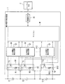
図1は、本実施形態における電池電圧検出装置1の構成概略図である。この図1に示すように、電池電圧検出装置1は、バッテリを構成する12個の電池セルC1〜C12のセル電圧を検出する機能及び各電池セルC1〜C12のセルバランス制御(セル電圧の均一化)を行う機能を備えたECU(Electronic Control Unit)であり、12個のバイパス回路B1〜B12と、12個のセル電圧検出回路D1〜D12と、マイコンM(電圧処理部)と、絶縁素子IRとを備えている。
Hereinafter, an embodiment of the present invention will be described with reference to the drawings.
FIG. 1 is a schematic configuration diagram of a battery
バイパス回路B1〜B12は、それぞれバイパス抵抗とトランジスタ等のスイッチング素子との直列回路からなり、電池セルC1〜C12のそれぞれに並列接続されている。なお、図1では、バイパス回路B1〜B12のそれぞれに内蔵されているバイパス抵抗の符号をR1〜R12とし、スイッチング素子の符号をT1〜T12としている。 Each of the bypass circuits B1 to B12 includes a series circuit of a bypass resistor and a switching element such as a transistor, and is connected in parallel to each of the battery cells C1 to C12. In FIG. 1, the signs of the bypass resistors built in the bypass circuits B1 to B12 are R1 to R12, and the signs of the switching elements are T1 to T12.
セル電圧検出回路D1〜D12は、電池セルC1〜C12のそれぞれに並列接続されており、それぞれに接続された電池セルの端子間電圧(セル電圧)を検出し、その検出したセル電圧をマイコンMに出力する。なお、詳細は後述するが、これらセル電圧検出回路D1〜D12は、電圧検出周期の1周期内において、それぞれ担当の電池セルによって2つのコンデンサ(フライングキャパシタ)を同時に充電した後、これら2つのフライングキャパシタの端子間電圧をセル電圧としてそれぞれ異なるタイミングでマイコンMへ出力するものである。 The cell voltage detection circuits D1 to D12 are connected in parallel to each of the battery cells C1 to C12. The cell voltage detection circuits D1 to D12 detect the voltage (cell voltage) between the terminals of the battery cells connected to each of the battery cells C1 to C12. Output to. Although details will be described later, these cell voltage detection circuits D1 to D12 charge two capacitors (flying capacitors) simultaneously with their respective battery cells within one cycle of the voltage detection cycle, and then perform these two flying operations. The voltage between the terminals of the capacitor is output to the microcomputer M at different timings as a cell voltage.
マイコンMは、ROM及びRAM等のメモリ、CPU(Central Processing Unit)、A/D変換回路、入出力インターフェースなどが一体的に組み込まれたマイクロコントローラであり、電圧検出周期の1周期内に、セル電圧検出回路D1〜D12のそれぞれから異なるタイミングで得られた2つのセル電圧に基づいてセル電圧の誤検出が発生したか否か(つまりセル電圧検出回路に異常が発生したか否か)を判断する機能を有している。 The microcomputer M is a microcontroller in which a memory such as a ROM and a RAM, a CPU (Central Processing Unit), an A / D conversion circuit, an input / output interface, and the like are integrated, and within one cycle of the voltage detection cycle. It is determined whether or not an erroneous detection of the cell voltage has occurred (that is, whether or not an abnormality has occurred in the cell voltage detection circuit) based on two cell voltages obtained at different timings from the voltage detection circuits D1 to D12. It has a function to do.
また、このマイコンMは、絶縁素子IRを介して上位制御装置であるバッテリECU2と通信可能に接続されており、各電池セルC1〜C12のセル電圧検出結果をバッテリECU2へ送信する機能を有している。なお、各電池セルC1〜C12のセル電圧は、電圧検出周期の1周期内でそれぞれ2つずつ得られるが、セル電圧の誤検出が発生していない場合(セル電圧検出回路が正常な場合)には、2つのセル電圧はほぼ等しくなるので、いずれか一方のセル電圧(例えばフライングキャパシタFC1から得られるセル電圧)をその電池セルのセル電圧検出結果としてバッテリECU2へ送信すれば良い。
Further, the microcomputer M is communicably connected to the
バッテリECU2は、マイコンMから受信した各電池セルC1〜C12のセル電圧検出結果を基にセル電圧のバランス状態を監視し、他の電池セルと比較してセル電圧の高い電池セルを発見すると、その電池セルを放電が必要なセル(要放電セル)として特定し、その特定結果をマイコンMに送信するものである。マイコンMは、バッテリECU2から要放電セルの特定結果を受信すると、要放電セルに接続されたバイパス回路に所定の放電電流が流れるよう、要放電セルに接続されたバイパス回路のスイッチング素子をデューティ制御する機能、つまりセルバランス制御機能を有している。
The
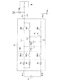
図2は、電池セルC1のセル電圧を検出するセル電圧検出回路D1の回路構成図である。なお、他のセル電圧検出回路D2〜D12も同様な回路構成であるので、以下ではセル電圧検出回路D1を代表的に用いてその回路構成の詳細について説明する。この図2において、符号Pi1は、電池セルC1の正極端子に接続される第1入力端子である。符号Pi2は、電池セルC1の負極端子に接続される第2入力端子である。符号Po1は、マイコンMの入力ポート(A/D変換回路に通じるポート)に接続される第1出力端子である。符号Po2は、電池電圧検出装置1内の共通電位線(例えばグランドラインSG)に接続される第2出力端子である。
FIG. 2 is a circuit configuration diagram of the cell voltage detection circuit D1 that detects the cell voltage of the battery cell C1. Since the other cell voltage detection circuits D2 to D12 have the same circuit configuration, the details of the circuit configuration will be described below using the cell voltage detection circuit D1 as a representative. In FIG. 2, the symbol Pi1 is a first input terminal connected to the positive terminal of the battery cell C1. Reference sign Pi2 is a second input terminal connected to the negative terminal of the battery cell C1. A symbol Po1 is a first output terminal connected to an input port of the microcomputer M (port connected to the A / D conversion circuit). The symbol Po2 is a second output terminal connected to a common potential line (for example, the ground line SG) in the battery
符号FC1は、第1入力端子Pi1と第1出力端子Po1とを結ぶ第1高電位線L1と、第2入力端子Pi2と第2出力端子Po2とを結ぶ低電位線L3との間に接続された第1フライングキャパシタ(第1コンデンサ)である。符号FC2は、上記第1高電位線L1に並列接続された第2高電位線L2と上記低電位線L3との間に接続された第2フライングキャパシタ(第2コンデンサ)である。 The code FC1 is connected between a first high potential line L1 connecting the first input terminal Pi1 and the first output terminal Po1, and a low potential line L3 connecting the second input terminal Pi2 and the second output terminal Po2. The first flying capacitor (first capacitor). Reference numeral FC2 denotes a second flying capacitor (second capacitor) connected between the second high potential line L2 connected in parallel to the first high potential line L1 and the low potential line L3.
符号SW1は、第1高電位線L1、第2高電位線L2及び低電位線L3における第1及び第2フライングキャパシタFC1、FC2の前段側に介挿された第1スイッチ群である。具体的には、この第1スイッチ群SW1は、第1高電位線L1における第1フライングキャパシタFC1の前段側に介挿された第1スイッチSW1aと、第2高電位線L2における第2フライングキャパシタFC2の前段側に介挿された第1スイッチSW1bと、低電位線L3における第1及び第2フライングキャパシタFC1、FC2の前段側に介挿された第1スイッチSW1cとから構成されている。 The symbol SW1 is a first switch group that is inserted in front of the first and second flying capacitors FC1, FC2 in the first high potential line L1, the second high potential line L2, and the low potential line L3. Specifically, the first switch group SW1 includes a first switch SW1a inserted in front of the first flying capacitor FC1 in the first high potential line L1, and a second flying capacitor in the second high potential line L2. The first switch SW1b is inserted in front of the FC2, and the first switch SW1c is inserted in front of the first and second flying capacitors FC1 and FC2 in the low potential line L3.
なお、第1高電位線L1における第1スイッチSW1aの前段側には入力抵抗Raが介挿され、第2高電位線L2における第1スイッチSW1bの前段側には入力抵抗Rbが介挿され、低電位線L3における第1スイッチSW1cの前段側には入力抵抗Rcが介挿されている。 An input resistor Ra is inserted on the first high potential line L1 in front of the first switch SW1a, and an input resistor Rb is inserted on the second high potential line L2 in front of the first switch SW1b. An input resistor Rc is inserted on the low-potential line L3 in front of the first switch SW1c.
符号SW2は、第1高電位線L1における第1フライングキャパシタFC1の後段側に介挿された第2スイッチである。符号SW3は、第2高電位線L2における第2フライングキャパシタFC2の後段側に介挿された第3スイッチである。符号SW4は、低電位線L3における第1及び第2フライングキャパシタFC1、FC2の後段側に介挿された第4スイッチである。 A symbol SW2 is a second switch inserted on the rear side of the first flying capacitor FC1 in the first high potential line L1. The symbol SW3 is a third switch inserted on the rear stage side of the second flying capacitor FC2 in the second high potential line L2. A symbol SW4 is a fourth switch inserted on the downstream side of the first and second flying capacitors FC1 and FC2 in the low potential line L3.
また、第1出力端子Po1とマイコンMとを接続する配線L4は、プルアップ抵抗Rpを介して電池電圧検出装置1内の電源ライン(例えばVcc=5Vの電源ライン)と接続されている。図示は省略しているが、この電源ラインは、回路動作の基準となる安定した基準電圧(Vcc)を生成する基準電圧源と接続されている。
Further, the wiring L4 that connects the first output terminal Po1 and the microcomputer M is connected to a power supply line (for example, a power supply line of Vcc = 5V) in the battery
なお、図2において、点線で示したリーク抵抗RLは実際の回路素子としてセル電圧検出回路D1内に存在しているわけではなく、セル電圧検出回路D1の経時劣化によって生じるリーク電流ILがどのような径路で流れるかを等価的に表すために図示したものである。セル電圧検出回路D1の経時劣化が進むと、リーク抵抗RLの値が小さくなってリーク電流ILが増大する。 In FIG. 2, the leak resistance RL indicated by the dotted line does not exist as an actual circuit element in the cell voltage detection circuit D1, but what is the leak current IL generated by the deterioration of the cell voltage detection circuit D1 with time? It is shown in order to represent equivalently whether the flow is in a proper path. As the cell voltage detection circuit D1 deteriorates with time, the value of the leakage resistance RL decreases and the leakage current IL increases.
以上が本実施形態における電池電圧検出装置1の構成に関する説明であり、以下では上記のように構成された電池電圧検出装置1の動作、特に本実施形態の特徴的な動作であるセル電圧の誤検出発生の有無(セル電圧検出回路の異常発生の有無)を判断する際の動作について、図3及び図4を参照しながら詳細に説明する。
なお、以下では、説明の便宜上、電池セルC1のセル電圧を検出するセル電圧検出回路D1を代表的に用いてセル電圧の誤検出発生の有無を判断する際の動作について説明するが、他のセル電圧検出回路D2〜D12についても同様な動作となる。
The above is the description regarding the configuration of the battery
In the following description, for convenience of explanation, the operation when determining whether or not the erroneous detection of the cell voltage has occurred will be described using the cell voltage detection circuit D1 that detects the cell voltage of the battery cell C1 as a representative. The cell voltage detection circuits D2 to D12 operate similarly.
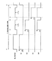
図3は、電圧検出周期Tdの1周期内における、セル電圧検出回路D1からマイコンMへ入力される検出電圧値V(つまりセル電圧検出回路D1の第1出力端子Po1と第2出力端子Po2との端子間電圧)と、セル電圧検出回路D1の第1スイッチ群SW1のオン/オフ状態と、第2スイッチSW2のオン/オフ状態と、第3スイッチSW3のオン/オフ状態と、第4スイッチSW4のオン/オフ状態との時間的な対応関係を示すタイミングチャートである。 FIG. 3 shows a detection voltage value V input from the cell voltage detection circuit D1 to the microcomputer M within one cycle of the voltage detection cycle Td (that is, the first output terminal Po1 and the second output terminal Po2 of the cell voltage detection circuit D1). Terminal voltage), the on / off state of the first switch group SW1 of the cell voltage detection circuit D1, the on / off state of the second switch SW2, the on / off state of the third switch SW3, and the fourth switch It is a timing chart which shows temporal correspondence with the ON / OFF state of SW4.
この図3に示すように、時刻t1に電圧検出周期Tdの開始タイミング(第1及び第2フライングキャパシタFC1、FC2の充電開始タイミング)が到来したと仮定すると、セル電圧検出回路D1の第1スイッチ群SW1(SW1a、SW1b、SW1c)がオン状態となる一方、第2スイッチSW2、第3スイッチSW3及び第4スイッチSW4がオフ状態となる。これにより、電池セルC1による第1及び第2フライングキャパシタFC1、FC2の充電が開始される。 As shown in FIG. 3, assuming that the start timing of the voltage detection cycle Td (charge start timing of the first and second flying capacitors FC1 and FC2) has arrived at time t1, the first switch of the cell voltage detection circuit D1 The group SW1 (SW1a, SW1b, SW1c) is turned on, while the second switch SW2, the third switch SW3, and the fourth switch SW4 are turned off. As a result, charging of the first and second flying capacitors FC1, FC2 by the battery cell C1 is started.
そして、第1スイッチ群SW1は、時刻t1から一定時間(第1及び第2フライングキャパシタFC1、FC2が十分に充電されたと考えられる時間)の経過後の時刻t2にオフ状態となる。時刻t1から時刻t2までの期間では、セル電圧検出回路D1とマイコンMとが電気的に切断された状態となるため、マイコンMにはプルアップ抵抗Rpを介してVccに相当する検出電圧値Vが入力される。 And 1st switch group SW1 will be in an OFF state at the time t2 after progress for a fixed time (time when 1st and 2nd flying capacitors FC1 and FC2 are fully charged) from the time t1. In the period from time t1 to time t2, since the cell voltage detection circuit D1 and the microcomputer M are electrically disconnected, the detection voltage value V corresponding to Vcc is supplied to the microcomputer M via the pull-up resistor Rp. Is entered.
そして、第1及び第2フライングキャパシタFC1、FC2の充電後、時刻t3から時刻t4までの期間において、第2スイッチSW2及び第4スイッチSW4がオン状態となる(第1スイッチ群SW1及び第3スイッチSW3はオフ状態)。これにより、時刻t3から時刻t4までの期間では、第1フライングキャパシタFC1の端子間電圧V_FC1に相当する検出電圧値VがマイコンMに入力される。 Then, after charging the first and second flying capacitors FC1 and FC2, the second switch SW2 and the fourth switch SW4 are turned on during the period from the time t3 to the time t4 (the first switch group SW1 and the third switch SW3 is off). Thereby, in the period from time t3 to time t4, the detected voltage value V corresponding to the inter-terminal voltage V_FC1 of the first flying capacitor FC1 is input to the microcomputer M.
この検出電圧値V(第1フライングキャパシタFC1の端子間電圧V_FC1)はマイコンM内に入力されると、A/D変換回路によってCPU処理可能なデジタルデータに変換され、マイコンM(正確にはCPU)は、時刻t3から時刻t4までの期間に得られた検出電圧値Vのデジタルデータを1つ目のセル電圧(以下、第1セル電圧V_FC1と称す)として内部メモリ(例えばRAM)に記憶する。 When this detected voltage value V (voltage V_FC1 between terminals of the first flying capacitor FC1) is input into the microcomputer M, it is converted into digital data that can be processed by the CPU by the A / D conversion circuit, and the microcomputer M (precisely CPU ) Stores the digital data of the detected voltage value V obtained during the period from time t3 to time t4 in the internal memory (for example, RAM) as the first cell voltage (hereinafter referred to as the first cell voltage V_FC1). .
そして、第1セル電圧V_FC1の取得後、時刻t5から時刻t6までの期間において、第3スイッチSW3及び第4スイッチSW4がオン状態となる(第1スイッチ群SW1及び第2スイッチSW2はオフ状態)。これにより、時刻t5から時刻t6までの期間では、第2フライングキャパシタFC2の端子間電圧V_FC2に相当する検出電圧値VがマイコンMに入力される。 Then, after obtaining the first cell voltage V_FC1, the third switch SW3 and the fourth switch SW4 are turned on during the period from the time t5 to the time t6 (the first switch group SW1 and the second switch SW2 are turned off). . As a result, during the period from time t5 to time t6, the detected voltage value V corresponding to the inter-terminal voltage V_FC2 of the second flying capacitor FC2 is input to the microcomputer M.
この検出電圧値V(第2フライングキャパシタFC2の端子間電圧V_FC2)はマイコンM内に入力されると、A/D変換回路によってCPU処理可能なデジタルデータに変換され、マイコンM(正確にはCPU)は、時刻t5から時刻t6までの期間に得られた検出電圧値Vのデジタルデータを2つ目のセル電圧(以下、第2セル電圧V_FC2と称す)として内部メモリ(例えばRAM)に記憶する。 When this detected voltage value V (voltage V_FC2 between the terminals of the second flying capacitor FC2) is input into the microcomputer M, it is converted into digital data that can be processed by the CPU by the A / D conversion circuit. ) Stores the digital data of the detected voltage value V obtained during the period from time t5 to time t6 in the internal memory (for example, RAM) as the second cell voltage (hereinafter referred to as the second cell voltage V_FC2). .
マイコンMは、上記のように、2つのセル電圧、つまり第1セル電圧V_FC1及び第2セル電圧V_FC2を取得すると、内部メモリからこれら第1セル電圧V_FC1及び第2セル電圧V_FC2を読み出して、第1セル電圧V_FC1と第2セル電圧V_FC2との差分ΔV(=V_FC1−V_FC2)を算出する。 As described above, when the microcomputer M acquires two cell voltages, that is, the first cell voltage V_FC1 and the second cell voltage V_FC2, the microcomputer M reads the first cell voltage V_FC1 and the second cell voltage V_FC2 from the internal memory, A difference ΔV (= V_FC1−V_FC2) between the 1 cell voltage V_FC1 and the second cell voltage V_FC2 is calculated.
図4(a)は、マイコンMに入力される検出電圧値Vと、セル電圧検出回路D1に発生するリーク電流IL(図2参照)との関係を示すV−IL特性図であり、図4(b)は、第1セル電圧V_FC1と第2セル電圧V_FC2との差分ΔVとリーク電流ILとの関係を示すΔV−IL特性図である。 4A is a V-IL characteristic diagram showing the relationship between the detection voltage value V input to the microcomputer M and the leakage current IL (see FIG. 2) generated in the cell voltage detection circuit D1. (B) is a ΔV-IL characteristic diagram showing the relationship between the difference ΔV between the first cell voltage V_FC1 and the second cell voltage V_FC2 and the leakage current IL.
これらの図からわかるように、セル電圧検出回路D1の経時劣化によってリーク電流ILが増大するほど、第1セル電圧V_FC1及び第2セル電圧V_FC2には、電池セルC1のセル電圧の真値に対して大きな誤差が発生し、第1セル電圧V_FC1と第2セル電圧V_FC2との差分ΔVが大きくなる。従って、この差分ΔVが最低限許容される閾値Vthを越えた時に、セル電圧の誤検出が発生した(セル電圧検出回路D1の異常が発生した)と判断することができる。 As can be seen from these drawings, the first cell voltage V_FC1 and the second cell voltage V_FC2 have a value relative to the true value of the cell voltage of the battery cell C1 as the leakage current IL increases due to the aging of the cell voltage detection circuit D1. A large error occurs, and the difference ΔV between the first cell voltage V_FC1 and the second cell voltage V_FC2 increases. Therefore, when the difference ΔV exceeds the minimum allowable threshold value Vth, it can be determined that an erroneous detection of the cell voltage has occurred (an abnormality of the cell voltage detection circuit D1 has occurred).
つまり、マイコンMは、上記のように算出した第1セル電圧V_FC1と第2セル電圧V_FC2との差分ΔVが閾値Vthを越えたか否かを判定し、差分ΔVが閾値Vthを越えた場合には、セル電圧の誤検出が発生した(セル電圧検出回路D1の異常が発生した)と判断して故障フラグを「1」にセットする一方、差分ΔVが閾値Vth以下の場合には、セル電圧を正常に検出した(セル電圧検出回路D1は正常)と判断して故障フラグを「0」にセットする(図4(c)参照)。 That is, the microcomputer M determines whether or not the difference ΔV between the first cell voltage V_FC1 and the second cell voltage V_FC2 calculated as described above exceeds the threshold value Vth, and when the difference ΔV exceeds the threshold value Vth. When it is determined that an erroneous detection of the cell voltage has occurred (abnormality of the cell voltage detection circuit D1 has occurred) and the failure flag is set to “1”, if the difference ΔV is less than or equal to the threshold value Vth, the cell voltage is The failure flag is set to “0” by determining that the detection is normal (the cell voltage detection circuit D1 is normal) (see FIG. 4C).
マイコンMは、故障フラグを「0」にセットした場合は、第1セル電圧V_FC1と第2セル電圧V_FC2とのいずれか一方を、電池セルC1のセル電圧検出結果としてバッテリECU2へ送信し、故障フラグを「1」にセットした場合は、電池セルC1のセル電圧検出結果の代わりに故障フラグをバッテリECU2へ送信することで、セル電圧の誤検出が発生した(セル電圧検出回路D1の異常が発生した)ことをバッテリECU2に知らせる。
When the failure flag is set to “0”, the microcomputer M transmits one of the first cell voltage V_FC1 and the second cell voltage V_FC2 to the
電池電圧検出装置1は、上述した一連の動作を電圧検出周期Tdで繰り返し実行することにより、各電池セルC1〜C12のセル電圧の誤検出発生(セル電圧検出回路D1〜D12の異常発生)を常時監視し、セル電圧の誤検出(セル電圧検出回路の異常)が発生した場合にはバッテリECU2に都度知らせることになる。なお、第1スイッチ群SW1、第2スイッチSW2、第3スイッチSW3及び第4スイッチSW4のオン/オフ状態は、マイコンMによって制御しても良いし、或いは他の制御回路を設けて制御しても良い。
The battery
以上のように、本実施形態によれば、セル電圧検出回路D1〜D12からそれぞれ異なるタイミングで得られた2つのセル電圧(第1セル電圧V_FC1と第2セル電圧V_FC2)に基づいてセル電圧の誤検出が発生したか否かを判断することにより、フライングキャパシタ式のセル電圧検出回路D1〜D12の経時劣化(リーク電流増加)に起因するセル電圧の誤検出発生(セル電圧検出回路の異常発生)を、簡単な構成で高精度に検知することができ、その結果、適切なバッテリ制御に寄与することができる。 As described above, according to the present embodiment, the cell voltage is determined based on the two cell voltages (first cell voltage V_FC1 and second cell voltage V_FC2) obtained from the cell voltage detection circuits D1 to D12 at different timings. By determining whether or not an erroneous detection has occurred, an erroneous detection of a cell voltage due to a time-dependent deterioration (an increase in leakage current) of the flying capacitor type cell voltage detection circuits D1 to D12 (an abnormal occurrence of the cell voltage detection circuit) ) Can be detected with high accuracy with a simple configuration, and as a result, it can contribute to appropriate battery control.
なお、本発明は上記実施形態に限定されず、以下のような変形例が挙げられる。
(1)上記実施形態では、第1及び第2フライングキャパシタFC1、FC2の充電後に、始めに第2スイッチSW2及び第4スイッチSW4がオン状態となって、次に第3スイッチSW3及び第4スイッチSW4がオン状態となる場合、つまり始めに第1フライングキャパシタFC1の端子間電圧V_FC1を取得し、次に第2フライングキャパシタFC2の端子間電圧V_FC2を取得する場合を例示した。
In addition, this invention is not limited to the said embodiment, The following modifications are mentioned.
(1) In the above embodiment, after charging the first and second flying capacitors FC1 and FC2, the second switch SW2 and the fourth switch SW4 are first turned on, and then the third switch SW3 and the fourth switch The case where SW4 is turned on, that is, the case where the voltage V_FC1 between the terminals of the first flying capacitor FC1 is first acquired and the voltage V_FC2 between the terminals of the second flying capacitor FC2 is acquired next is illustrated.
これに対して、第1及び第2フライングキャパシタFC1、FC2の充電後に、始めに第3スイッチSW3及び第4スイッチSW4をオン状態とし、次に第2スイッチSW2及び第4スイッチSW4をオン状態とする、つまり始めに第2フライングキャパシタFC2の端子間電圧V_FC2を取得し、次に第1フライングキャパシタFC1の端子間電圧V_FC1を取得するようにしても良い。
また、上記実施形態では、第1スイッチ群SW1のうち全てのスイッチ(SW1a、SW1b、SW1c)をオンオフ制御するようにしているが、第1スイッチ群SW1のうち各々のスイッチ(SW1a、SW1b、SW1c)をオンオフ制御するようにしても良い。
On the other hand, after charging the first and second flying capacitors FC1 and FC2, the third switch SW3 and the fourth switch SW4 are first turned on, and then the second switch SW2 and the fourth switch SW4 are turned on. That is, first, the terminal voltage V_FC2 of the second flying capacitor FC2 may be acquired, and then the terminal voltage V_FC1 of the first flying capacitor FC1 may be acquired.
In the above embodiment, all the switches (SW1a, SW1b, SW1c) in the first switch group SW1 are on / off controlled. However, each switch (SW1a, SW1b, SW1c) in the first switch group SW1 is controlled. ) May be on / off controlled.
(2)上記実施形態では、図2を参照しながらセル電圧検出回路D1〜D12の回路構成の一例を説明したが、セル電圧検出回路D1〜D12の回路構成はこれに限らず、電池セルによって2つのコンデンサ(フライングキャパシタ)を同時に充電した後、2つのコンデンサの端子間電圧をセル電圧としてそれぞれ異なるタイミングでマイコンMへ出力する回路構成であれば、どのようなものでも良い。また、1つのセル電圧検出回路にフライングキャパシタを3つ以上設けても良い。 (2) In the above embodiment, an example of the circuit configuration of the cell voltage detection circuits D1 to D12 has been described with reference to FIG. 2, but the circuit configuration of the cell voltage detection circuits D1 to D12 is not limited to this, and depending on the battery cell Any circuit configuration may be used as long as the two capacitors (flying capacitors) are charged simultaneously and the voltage between the terminals of the two capacitors is output as a cell voltage to the microcomputer M at different timings. Further, three or more flying capacitors may be provided in one cell voltage detection circuit.
(3)上記実施形態では、12個の電池セルC1〜C12についてセル電圧検出を行う電池電圧検出装置1を例示したが、測定対象の電池セル数は12個に限定されない。また、セル電圧検出回路D1〜D12も電池セルC1〜C12に対応して12個設ける場合を例示したが、セル電圧検出回路を1個だけ設け、マルチプレクサによって電池セルC1〜C12のそれぞれの両端子とセル電圧検出回路の両入力端子(第1入力端子Pi1、第2入力端子Pi2)とを順次接続させながら、各電池セルC1〜C12のセル電圧を順番に検出するような構成としても良い。なお、マルチプレクサを使用する場合、第1スイッチ群SW1は不要となる。
(3) In the said embodiment, although the battery
1…電池電圧検出装置、C1〜C12…電池セル、B1〜B12…バイパス回路、D1〜D12…セル電圧検出回路、M…マイコン(電圧管理部)、Pi1…第1入力端子、Pi2…第2入力端子、Po1…第1出力端子、Po2…第2出力端子、FC1…第1フライングキャパシタ(第1コンデンサ)、FC2…第2フライングキャパシタ(第2コンデンサ)、SW1…第1スイッチ群、SW2…第2スイッチ、SW3…第3スイッチ、SW4…第4スイッチ
DESCRIPTION OF
Claims (3)
前記電圧検出回路は、前記電池セルによって同時に充電される複数のコンデンサを有し、充電後に前記複数のコンデンサの端子間電圧を前記セル電圧としてそれぞれ異なるタイミングで前記電圧処理部へ出力し、
前記電圧処理部は、前記電圧検出回路から異なるタイミングで得られた複数のセル電圧に基づいて前記セル電圧の誤検出が発生したか否かを判断することを特徴とする電池電圧検出装置。 A battery voltage detection device comprising: a voltage detection circuit that detects a cell voltage of a battery cell; and a voltage processing unit that processes a detection result of the cell voltage,
The voltage detection circuit has a plurality of capacitors that are simultaneously charged by the battery cell, and outputs the voltage between the terminals of the plurality of capacitors after charging to the voltage processing unit at different timings as the cell voltage,
The voltage processing unit determines whether or not an erroneous detection of the cell voltage has occurred based on a plurality of cell voltages obtained at different timings from the voltage detection circuit.
各電圧検出回路のそれぞれは、
前記電池セルの正極端子に接続される第1入力端子と、
前記電池セルの負極端子に接続される第2入力端子と、
前記電圧処理部に接続される第1出力端子と、
共通電位線に接続される第2出力端子と、
前記第1入力端子と前記第1出力端子とを結ぶ第1高電位線と、前記第2入力端子と前記第2出力端子とを結ぶ低電位線との間に接続された第1コンデンサと、
前記第1高電位線に並列接続された第2高電位線と前記低電位線との間に接続された第2コンデンサと、
前記第1高電位線、前記第2高電位線及び前記低電位線における前記第1及び第2コンデンサの前段側に介挿された第1スイッチ群と、
前記第1高電位線における前記第1コンデンサの後段側に介挿された第2スイッチと、
前記第2高電位線における前記第2コンデンサの後段側に介挿された第3スイッチと、
前記低電位線における前記第1及び第2コンデンサの後段側に介挿された第4スイッチと、を備え、
前記第1及び第2コンデンサの充電時には、前記第1スイッチ群のうち各々または全てがオン状態に、前記第2、第3及び第4スイッチがオフ状態となり、
前記第1及び第2コンデンサの充電後には、始めに前記第2及び第4スイッチがオン状態となって、次に前記第3及び第4スイッチがオン状態となるか、或いは始めに前記第3及び第4スイッチがオン状態となって、次に前記第2及び第4スイッチがオン状態となることを特徴とする請求項1または2に記載の電池電圧検出装置。 The voltage detection circuit is individually provided for each of the plurality of battery cells connected in series,
Each voltage detection circuit
A first input terminal connected to the positive terminal of the battery cell;
A second input terminal connected to the negative terminal of the battery cell;
A first output terminal connected to the voltage processing unit;
A second output terminal connected to the common potential line;
A first capacitor connected between a first high potential line connecting the first input terminal and the first output terminal and a low potential line connecting the second input terminal and the second output terminal;
A second capacitor connected between the second high potential line connected in parallel to the first high potential line and the low potential line;
A first switch group interposed in front of the first and second capacitors in the first high potential line, the second high potential line, and the low potential line;
A second switch interposed on the rear side of the first capacitor in the first high potential line;
A third switch interposed on the second stage of the second capacitor in the second high potential line;
A fourth switch interposed on the rear side of the first and second capacitors in the low potential line,
At the time of charging the first and second capacitors, each or all of the first switch group is turned on, and the second, third and fourth switches are turned off,
After charging the first and second capacitors, the second and fourth switches are first turned on, and then the third and fourth switches are turned on, or first the third capacitors are turned on. 3. The battery voltage detection device according to claim 1, wherein the second and fourth switches are turned on, and then the second and fourth switches are turned on. 4.
Priority Applications (3)
| Application Number | Priority Date | Filing Date | Title |
|---|---|---|---|
| JP2011075302A JP2012208066A (en) | 2011-03-30 | 2011-03-30 | Battery voltage detection device |
| EP12161352A EP2508905A2 (en) | 2011-03-30 | 2012-03-26 | Battery voltage detector |
| CN2012100852337A CN102735898A (en) | 2011-03-30 | 2012-03-28 | Battery voltage detector |
Applications Claiming Priority (1)
| Application Number | Priority Date | Filing Date | Title |
|---|---|---|---|
| JP2011075302A JP2012208066A (en) | 2011-03-30 | 2011-03-30 | Battery voltage detection device |
Publications (1)
| Publication Number | Publication Date |
|---|---|
| JP2012208066A true JP2012208066A (en) | 2012-10-25 |
Family
ID=45976701
Family Applications (1)
| Application Number | Title | Priority Date | Filing Date |
|---|---|---|---|
| JP2011075302A Pending JP2012208066A (en) | 2011-03-30 | 2011-03-30 | Battery voltage detection device |
Country Status (3)
| Country | Link |
|---|---|
| EP (1) | EP2508905A2 (en) |
| JP (1) | JP2012208066A (en) |
| CN (1) | CN102735898A (en) |
Cited By (4)
| Publication number | Priority date | Publication date | Assignee | Title |
|---|---|---|---|---|
| JP2017120253A (en) * | 2015-12-24 | 2017-07-06 | 矢崎総業株式会社 | Difference voltage measurement device |
| JP2017156297A (en) * | 2016-03-04 | 2017-09-07 | トヨタ自動車株式会社 | Voltage detector |
| JP2018116012A (en) * | 2017-01-20 | 2018-07-26 | 矢崎総業株式会社 | Differential voltage measurement device |
| JP2020134465A (en) * | 2019-02-25 | 2020-08-31 | 株式会社デンソー | Voltage detection device |
Families Citing this family (3)
| Publication number | Priority date | Publication date | Assignee | Title |
|---|---|---|---|---|
| CN105953107B (en) * | 2016-07-22 | 2019-07-09 | 厦门普为光电科技有限公司 | Light emitting diode emergency light and its operating method with signal switch mode |
| KR102410938B1 (en) * | 2017-06-20 | 2022-06-20 | 현대자동차주식회사 | Apparatus for managing power of vehicle and method for controlling the same |
| CN114690503B (en) * | 2020-12-28 | 2024-02-06 | 北京小米移动软件有限公司 | Mobile terminal and control method thereof |
Citations (5)
| Publication number | Priority date | Publication date | Assignee | Title |
|---|---|---|---|---|
| JPS63283421A (en) * | 1987-05-13 | 1988-11-21 | Mitsubishi Electric Corp | Protective relay |
| JP2001201522A (en) * | 2000-01-19 | 2001-07-27 | Hitachi Ltd | Cell voltage detecting circuit of multi-cell series battery and battery pack by using it |
| JP2002315212A (en) * | 2001-04-13 | 2002-10-25 | Denso Corp | Apparatus for detecting voltage of flying capacitor combined battery set |
| JP2009100551A (en) * | 2007-10-17 | 2009-05-07 | Yokogawa Electric Corp | Current detector |
| JP2010203790A (en) * | 2009-02-27 | 2010-09-16 | Toyota Motor Corp | Overcharge detection device for on-vehicle secondary battery |
Family Cites Families (8)
| Publication number | Priority date | Publication date | Assignee | Title |
|---|---|---|---|---|
| JP2001204141A (en) * | 2000-01-19 | 2001-07-27 | Hitachi Ltd | Detector for cell voltage of set battery and detecting method therefor |
| JP4099954B2 (en) | 2001-03-27 | 2008-06-11 | 株式会社デンソー | Flying capacitor type assembled battery voltage detector |
| JP3791767B2 (en) * | 2001-03-27 | 2006-06-28 | 株式会社デンソー | Flying capacitor voltage detection circuit |
| JP4339024B2 (en) * | 2003-06-09 | 2009-10-07 | サンケン電気株式会社 | Voltage measuring device |
| JP4509852B2 (en) * | 2005-05-17 | 2010-07-21 | 株式会社東芝 | Battery assembly and voltage detector |
| JP4520925B2 (en) * | 2005-10-03 | 2010-08-11 | 矢崎総業株式会社 | Voltage measuring device |
| JP4820739B2 (en) * | 2006-12-07 | 2011-11-24 | オンセミコンダクター・トレーディング・リミテッド | Battery voltage detection circuit |
| JP2010145128A (en) * | 2008-12-16 | 2010-07-01 | Denso Corp | Device for monitoring battery pack |
-
2011
- 2011-03-30 JP JP2011075302A patent/JP2012208066A/en active Pending
-
2012
- 2012-03-26 EP EP12161352A patent/EP2508905A2/en not_active Withdrawn
- 2012-03-28 CN CN2012100852337A patent/CN102735898A/en active Pending
Patent Citations (5)
| Publication number | Priority date | Publication date | Assignee | Title |
|---|---|---|---|---|
| JPS63283421A (en) * | 1987-05-13 | 1988-11-21 | Mitsubishi Electric Corp | Protective relay |
| JP2001201522A (en) * | 2000-01-19 | 2001-07-27 | Hitachi Ltd | Cell voltage detecting circuit of multi-cell series battery and battery pack by using it |
| JP2002315212A (en) * | 2001-04-13 | 2002-10-25 | Denso Corp | Apparatus for detecting voltage of flying capacitor combined battery set |
| JP2009100551A (en) * | 2007-10-17 | 2009-05-07 | Yokogawa Electric Corp | Current detector |
| JP2010203790A (en) * | 2009-02-27 | 2010-09-16 | Toyota Motor Corp | Overcharge detection device for on-vehicle secondary battery |
Cited By (5)
| Publication number | Priority date | Publication date | Assignee | Title |
|---|---|---|---|---|
| JP2017120253A (en) * | 2015-12-24 | 2017-07-06 | 矢崎総業株式会社 | Difference voltage measurement device |
| JP2017156297A (en) * | 2016-03-04 | 2017-09-07 | トヨタ自動車株式会社 | Voltage detector |
| JP2018116012A (en) * | 2017-01-20 | 2018-07-26 | 矢崎総業株式会社 | Differential voltage measurement device |
| JP2020134465A (en) * | 2019-02-25 | 2020-08-31 | 株式会社デンソー | Voltage detection device |
| JP7293714B2 (en) | 2019-02-25 | 2023-06-20 | 株式会社デンソー | voltage detector |
Also Published As
| Publication number | Publication date |
|---|---|
| EP2508905A2 (en) | 2012-10-10 |
| CN102735898A (en) | 2012-10-17 |
Similar Documents
| Publication | Publication Date | Title |
|---|---|---|
| JP2012208067A (en) | Battery voltage detection device | |
| JP6093106B2 (en) | Battery voltage detector | |
| KR102446380B1 (en) | Method and battery management sytem for cell balancing | |
| KR102150147B1 (en) | Apparatus and method for balancing battery module | |
| KR101453786B1 (en) | Apparatus for measuring isolation resistance having malfunction self -diagnosing function and malfunction self-diagnosing method using the same | |
| US10620274B2 (en) | Method and apparatus for contact detection in battery packs | |
| US20150077124A1 (en) | Assembled battery module and disconnection detecting method | |
| US9716520B2 (en) | Integrated standard-compliant data acquisition device | |
| JP2012208066A (en) | Battery voltage detection device | |
| KR20130109066A (en) | Apparatus and method for measuring isolation resistance of battery | |
| JP5974849B2 (en) | Battery monitoring device | |
| JP5569418B2 (en) | Battery monitoring device | |
| WO2017110578A1 (en) | Current monitoring circuit and coulomb counter circuit, and battery management system and motor vehicle using same | |
| JP2009286292A (en) | Vehicular power supply device | |
| US20160172720A1 (en) | Method and Apparatus for Contact Detection in Battery Packs | |
| JP2017070024A (en) | Battery monitoring device | |
| US11130406B2 (en) | Integrated standard-compliant data acquisition device | |
| KR101473395B1 (en) | Apparatus for measuring isolation resistance having malfunction self-diagnosing and method thereof | |
| JP2016152720A (en) | Cell balance circuit and failure diagnosis device thereof | |
| JP2014206453A (en) | Battery monitoring device | |
| JP5764456B2 (en) | Battery monitoring device | |
| KR101475914B1 (en) | Apparatus for measuring isolation resistance having malfunction self-diagnosing and method thereof | |
| JP2015102336A (en) | Battery monitoring device | |
| JP2016075557A (en) | Battery monitoring circuit and battery module | |
| JP7467337B2 (en) | Integrated circuit, battery monitoring device, and battery monitoring system |
Legal Events
| Date | Code | Title | Description |
|---|---|---|---|
| A621 | Written request for application examination |
Free format text: JAPANESE INTERMEDIATE CODE: A621 Effective date: 20140203 |
|
| A977 | Report on retrieval |
Free format text: JAPANESE INTERMEDIATE CODE: A971007 Effective date: 20140905 |
|
| A131 | Notification of reasons for refusal |
Free format text: JAPANESE INTERMEDIATE CODE: A131 Effective date: 20141111 |
|
| A521 | Written amendment |
Free format text: JAPANESE INTERMEDIATE CODE: A523 Effective date: 20150107 |
|
| A02 | Decision of refusal |
Free format text: JAPANESE INTERMEDIATE CODE: A02 Effective date: 20150707 |