JP2012205455A - Method of controlling switching power supply in the case of light load or no load, and switching power supply - Google Patents
Method of controlling switching power supply in the case of light load or no load, and switching power supply Download PDFInfo
- Publication number
- JP2012205455A JP2012205455A JP2011069916A JP2011069916A JP2012205455A JP 2012205455 A JP2012205455 A JP 2012205455A JP 2011069916 A JP2011069916 A JP 2011069916A JP 2011069916 A JP2011069916 A JP 2011069916A JP 2012205455 A JP2012205455 A JP 2012205455A
- Authority
- JP
- Japan
- Prior art keywords
- switching element
- voltage
- reference voltage
- output voltage
- power supply
- Prior art date
- Legal status (The legal status is an assumption and is not a legal conclusion. Google has not performed a legal analysis and makes no representation as to the accuracy of the status listed.)
- Granted
Links
Images


Landscapes
- Dc-Dc Converters (AREA)
Abstract
Description
本発明の実施形態は、軽負荷または無負荷時におけるスイッチング電源の制御方法およびスイッチング電源に関する。 Embodiments described herein relate generally to a switching power supply control method and a switching power supply during light load or no load.
従来のスイッチング電源は、所望の電圧を出力する入力源と、この入力源に接続された第1のスイッチング素子と、この第1のスイッチング素子と接地との間に、互いに並列に接続された第2のスイッチング素子およびダイオードと、これらのスイッチ間に一端が接続されたチョークコイルと、このコイルの他端と接地と間に接続されたコンデンサと、を具備し、コンデンサ間に発生する電圧を、出力電圧として負荷に供給する。 A conventional switching power supply includes an input source that outputs a desired voltage, a first switching element connected to the input source, and a first switching element connected in parallel to each other between the first switching element and the ground. Two switching elements and diodes, a choke coil having one end connected between these switches, and a capacitor connected between the other end of the coil and the ground, and a voltage generated between the capacitors, Supply to load as output voltage.
このスイッチング電源において、軽負荷または無負荷時における第1、第2のスイッチング素子は、以下のように制御される。 In this switching power supply, the first and second switching elements at the time of light load or no load are controlled as follows.
第1に、出力電圧が規定値より大きいとき、第1、第2のスイッチング素子が共に非導通となるように制御される。これにより、コンデンサに充電された電力は負荷から放電されるため、出力電圧は低下する。 First, when the output voltage is larger than a specified value, the first and second switching elements are controlled so as to be non-conductive. Thereby, since the electric power charged in the capacitor is discharged from the load, the output voltage decreases.
第2に、出力電圧が設定値より小さいとき、第2のスイッチング素子を非導通にしたまま、第1のスイッチング素子のみをスイッチングするように制御される。これにより、第1のスイッチング素子が導通するときにコンデンサに電力が充電されるため、出力電圧は上昇する。 Secondly, when the output voltage is smaller than the set value, control is performed so that only the first switching element is switched while the second switching element is kept non-conductive. As a result, the power is charged in the capacitor when the first switching element is turned on, and the output voltage rises.
このような従来のスイッチング電源において、以下の問題がある。第1に、出力電圧が規定値より大きいとき、第1、第2のスイッチング素子を共に非導通した状態でキャパシタに充電された電力を負荷から放電するため、放電時間が長く、スイッチング電源の応答速度が遅い問題がある。特に、コンデンサとして、大容量のコンデンサが適用されている場合、放電時間は非常に長くなる。 Such a conventional switching power supply has the following problems. First, when the output voltage is larger than a specified value, the power charged in the capacitor is discharged from the load while both the first and second switching elements are in a non-conductive state. There is a problem of slow speed. In particular, when a large-capacity capacitor is used as the capacitor, the discharge time becomes very long.
第2に、出力電圧が規定値より小さいとき、第2のスイッチング素子を非導通にしたままの状態で第1のスイッチング素子のみをスイッチングさせると、第1、第2のスイッチング素子が共に非導通のときにダイオードに電流が流れるため、ダイオードにおいて電圧降下が発生し、電源内部で電力が損失する問題がある。 Second, when only the first switching element is switched while the second switching element is kept non-conductive when the output voltage is smaller than the specified value, both the first and second switching elements are non-conductive. In this case, since a current flows through the diode, a voltage drop occurs in the diode, and there is a problem that power is lost inside the power supply.
本発明の実施形態は、応答速度を向上させ、かつ電力の内部損失を低減することができる軽負荷または、無負荷時におけるスイッチング電源の制御方法およびスイッチング電源を提供することを目的とする。 Embodiments of the present invention have an object to provide a switching power supply control method and a switching power supply during light load or no load that can improve response speed and reduce internal loss of power.
本発明の実施形態に係る無負荷または軽負荷時におけるスイッチング電源の制御方法は、インダクタンス素子、ダイオード、コンデンサ、第1のスイッチング素子、および前記ダイオードと並列に配置された第2のスイッチング素子を有する無負荷または軽負荷時における降圧型、または昇圧型のスイッチング電源の制御方法であって、前記スイッチング電源の出力電圧が、第1の基準電圧と、この電圧より大きい電圧である第2の基準電圧と、によって定められる基準電圧の範囲内であるか否かを判定するステップと、このステップによる判定結果に基づいて、前記出力電圧が、前記基準電圧の範囲内になるように、前記第1のスイッチング素子および前記第2のスイッチング素子の動作を制御するステップと、を具備し、前記第1のスイッチング素子および前記第2のスイッチング素子を制御するステップは、前記出力電圧が前記第1の基準電圧より小さい場合は、前記第1のスイッチング素子の一度の導通によって増加する前記出力電圧の量が、前記第1の基準電圧と前記第2の基準電圧との差分電圧より小さくなるように、前記第1のスイッチング素子をスイッチングさせるとともに、前記第1のスイッチング素子と前記第2のスイッチング素子とが同時に導通せず、かつ前記インダクタンス素子に電流が流れているタイミングで前記第2のスイッチング素子が導通するように、前記第2のスイッチング素子をスイッチング動作させ、前記出力電圧が前記第2の基準電圧より大きい場合は、前記第2のスイッチング素子の一度の導通によって減少する前記出力電圧の量が、前記差分電圧より小さくなるように、前記第2のスイッチング素子をスイッチングさせる。 A method for controlling a switching power supply during no load or light load according to an embodiment of the present invention includes an inductance element, a diode, a capacitor, a first switching element, and a second switching element arranged in parallel with the diode. A method of controlling a step-down or step-up switching power supply at the time of no load or light load, wherein an output voltage of the switching power supply is a first reference voltage and a second reference voltage greater than this voltage. Determining whether the output voltage is within the range of the reference voltage determined based on the determination result of the step and the first voltage so that the output voltage is within the range of the reference voltage. And a step of controlling operations of the switching element and the second switching element. When the output voltage is smaller than the first reference voltage, the step of controlling the chucking element and the second switching element includes an amount of the output voltage that is increased by one conduction of the first switching element. The first switching element is switched so as to be smaller than a differential voltage between the first reference voltage and the second reference voltage, and the first switching element and the second switching element are simultaneously The second switching element is switched so that the second switching element is conductive at a timing when current is flowing through the inductance element, and the output voltage is higher than the second reference voltage. If the output voltage is large, the amount of the output voltage that is reduced by one conduction of the second switching element is Serial differential voltage so than decreases, thereby switching the second switching element.
また、本発明の実施形態に係る無負荷または軽負荷時におけるスイッチング電源の制御方法は、インダクタンス素子、ダイオード、コンデンサ、第1のスイッチング素子、および前記ダイオードと並列に配置された第2のスイッチング素子を有する無負荷または軽負荷時における反転型のスイッチング電源の制御方法であって、前記スイッチング電源の出力電圧が、第1の基準電圧と、この電圧より大きい電圧である第2の基準電圧と、によって定められる基準電圧の範囲内であるか否かを判定するステップと、このステップよる判定結果に基づいて、前記出力電圧が、前記基準電圧の範囲内になるように、前記第1のスイッチング素子および前記第2のスイッチング素子の動作を制御するステップと、を具備し、前記第1のスイッチング素子および前記第2のスイッチング素子を制御するステップは、前記出力電圧が前記第1の基準電圧より小さい場合は、前記第2のスイッチング素子の一度の導通によって増加する前記出力電圧の量が、前記差分電圧より小さくなるように、前記第2のスイッチング素子をスイッチングさせ、前記出力電圧が前記第2の基準電圧より大きい場合は、前記第1のスイッチング素子の一度の導通によって減少する前記出力電圧の量が、前記第1の基準電圧と前記第2の基準電圧との差分電圧より小さくなるように、前記第1のスイッチング素子をスイッチングさせるとともに、前記第1のスイッチング素子と前記第2のスイッチング素子とが同時に導通せず、かつ前記インダクタンス素子に電流が流れているタイミングで前記第2のスイッチング素子が導通するように、前記第2のスイッチング素子をスイッチング動作させる。 In addition, according to the embodiment of the present invention, there is provided a method for controlling a switching power supply during no load or light load, including an inductance element, a diode, a capacitor, a first switching element, and a second switching element arranged in parallel with the diode. A control method for an inverting switching power supply at the time of no load or light load having an output voltage of the switching power supply of a first reference voltage and a second reference voltage that is higher than this voltage, And determining whether the output voltage is within the range of the reference voltage based on the determination result of the step. And a step of controlling the operation of the second switching element, and the first switching element. And the step of controlling the second switching element includes a step in which, when the output voltage is smaller than the first reference voltage, the amount of the output voltage that is increased by one conduction of the second switching element is the difference. When the second switching element is switched so as to be smaller than the voltage, and the output voltage is larger than the second reference voltage, the amount of the output voltage that decreases by one-time conduction of the first switching element Switching the first switching element so as to be smaller than a differential voltage between the first reference voltage and the second reference voltage, and the first switching element and the second switching element, Are not conducted at the same time, and the second switching element is at a timing when current flows through the inductance element. So it conducts, the second switching element is a switching operation.
また、本発明の実施形態に係るスイッチング電源は、インダクタンス素子、ダイオード、コンデンサ、第1のスイッチング素子、および前記ダイオードと並列に配置された第2のスイッチング素子を有する降圧型、または昇圧型の電源本体と、この電源本体の出力端子と前記コンデンサとの間に接続され、前記出力端子に発生した出力電圧が、第1の基準電圧と、この電圧より大きい電圧である第2の基準電圧と、によって定められる基準電圧の範囲内であるか否かを判定する電圧判定部と、この電圧判定部に接続され、前記電圧判定部による判定結果に基づいて、前記出力電圧が、前記基準電圧の範囲内になるように、前記第1のスイッチング素子および前記第2のスイッチング素子の動作を制御するスイッチ駆動部と、を具備し、無負荷または軽負荷時における前記スイッチ駆動部は、前記出力電圧が前記第1の基準電圧より小さい場合は、前記第1のスイッチング素子の一度の導通によって増加する前記出力電圧の量が、前記第1の基準電圧と前記第2の基準電圧との差分電圧より小さくなるように、前記第1のスイッチング素子をスイッチングさせるとともに、前記第1のスイッチング素子と前記第2のスイッチング素子とが同時に導通せず、かつ前記インダクタンス素子に電流が流れているタイミングで前記第2のスイッチング素子が導通するように、前記第2のスイッチング素子をスイッチング動作させ、前記出力電圧が前記第2の基準電圧より大きい場合は、前記第2のスイッチング素子の一度の導通によって減少する前記出力電圧の量が、前記差分電圧より小さくなるように、前記第2のスイッチング素子をスイッチングさせる。 A switching power supply according to an embodiment of the present invention includes a step-down or step-up power supply having an inductance element, a diode, a capacitor, a first switching element, and a second switching element arranged in parallel with the diode. A main body, connected between the output terminal of the power source main body and the capacitor, and an output voltage generated at the output terminal is a first reference voltage, and a second reference voltage having a voltage higher than the first voltage; A voltage determination unit that determines whether or not the voltage is within a range of the reference voltage determined by the voltage determination unit, and the output voltage is connected to the voltage determination unit based on a determination result by the voltage determination unit. A switch driving unit for controlling the operation of the first switching element and the second switching element so as to be inward, and a no-load Alternatively, when the output voltage is smaller than the first reference voltage, the switch driving unit at a light load has an amount of the output voltage that is increased by one conduction of the first switching element. The first switching element is switched so that the difference voltage between the reference voltage and the second reference voltage becomes smaller, and the first switching element and the second switching element do not conduct at the same time. And when the second switching element is switched so that the second switching element becomes conductive at a timing when a current flows through the inductance element, and the output voltage is larger than the second reference voltage. The amount of the output voltage that is reduced by one-time conduction of the second switching element is smaller than the differential voltage. So that the causes switching the second switching element.
また、本発明の実施形態に係るスイッチング電源は、インダクタンス素子、ダイオード、コンデンサ、第1のスイッチング素子、および前記ダイオードと並列に配置された第2のスイッチング素子を有する反転型の電源本体と、この電源本体の出力端子と前記コンデンサとの間に接続され、前記出力端子に発生した出力電圧が、第1の基準電圧と、この電圧より大きい電圧である第2の基準電圧と、によって定められる基準電圧の範囲内であるか否かを判定する電圧判定部と、この電圧判定部に接続され、前記電圧判定部による判定結果に基づいて、前記出力電圧が、前記基準電圧の範囲内になるように、前記第1のスイッチング素子および前記第2のスイッチング素子の動作を制御するスイッチ駆動部と、を具備し、無負荷または軽負荷時における前記スイッチ駆動部は、前記出力電圧が前記第1の基準電圧より小さい場合は、前記第2のスイッチング素子の一度の導通によって増加する前記出力電圧の量が、前記差分電圧より小さくなるように、前記第2のスイッチング素子をスイッチングさせ、前記出力電圧が前記第2の基準電圧より大きい場合は、前記第1のスイッチング素子の一度の導通によって減少する前記出力電圧の量が、前記第1の基準電圧と前記第2の基準電圧との差分電圧より小さくなるように、前記第1のスイッチング素子をスイッチングさせるとともに、前記第1のスイッチング素子と前記第2のスイッチング素子とが同時に導通せず、かつ前記インダクタンス素子に電流が流れているタイミングで前記第2のスイッチング素子が導通するように、前記第2のスイッチング素子をスイッチング動作させる。 The switching power supply according to the embodiment of the present invention includes an inductance element, a diode, a capacitor, a first switching element, and an inverting power supply body having a second switching element arranged in parallel with the diode, A reference that is connected between the output terminal of the power supply body and the capacitor, and an output voltage generated at the output terminal is determined by a first reference voltage and a second reference voltage that is a voltage higher than the first reference voltage. A voltage determination unit that determines whether or not the voltage is within a voltage range, and the voltage determination unit that is connected to the voltage determination unit, so that the output voltage is within the reference voltage range based on a determination result by the voltage determination unit And a switch driving unit for controlling the operation of the first switching element and the second switching element, and at no load or light load When the output voltage is smaller than the first reference voltage, the switch driving unit in the switch is configured such that the amount of the output voltage that is increased by one conduction of the second switching element is smaller than the differential voltage. When the second switching element is switched and the output voltage is larger than the second reference voltage, the amount of the output voltage that is reduced by one conduction of the first switching element is the first voltage. The first switching element is switched so as to be smaller than a differential voltage between a reference voltage and the second reference voltage, and the first switching element and the second switching element do not conduct at the same time, And the second switching element is turned on at a timing when a current flows through the inductance element. The switching elements perform switching operation.
以下、本発明の実施の形態に係る軽負荷または、無負荷時におけるスイッチング電源の制御方法およびスイッチング電源について、図面を参照して説明する。 Hereinafter, a switching power supply control method and a switching power supply during light load or no load according to an embodiment of the present invention will be described with reference to the drawings.
(第1の実施形態)
図1は、第1の実施形態に係るスイッチング電源を示す図である。このスイッチング電源10は、いわゆるDC/DCコンバータであり、より詳しくは、同期整流方式の降圧型コンバータである。また、DC/DCコンバータの制御方式はデシタル制御方式である。
(First embodiment)
FIG. 1 is a diagram illustrating a switching power supply according to the first embodiment. The switching
図1に示すように、スイッチング電源10は、入力端子および出力端子を有しており、これらの端子間に、降圧型の電源本体10−1(以下、電源本体10−1と称する)を有する。電源本体10−1は、入力端子に入力源11が接続され、出力端子に負荷12が接続されると、入力源11から供給される電圧Vinを任意の出力電圧Voutに降圧して、負荷12に供給する。
As shown in FIG. 1, the
電源本体10−1は、第1のスイッチング素子としてのハイサイドFET13、および第2のスイッチング素子としてのローサイドFET14を有する。
The power supply body 10-1 has a
ハイサイドFET13のドレイン端子は、マイナス端子が接地された入力源11のプラス端子に接続される。ハイサイドFET13のソース端子は、ローサイドFET14のドレイン端子に接続される。また、ローサイドFET14のソース端子は接地される。
The drain terminal of the
なお、図1に示される電源本体10−1において、ハイサイドFET13はNチャンネルFETであるが、PチャンネルFETであってもよい。ハイサイドFET13としてPチャンネルFETを適用する場合、ソース端子が入力源11のプラス端子に接続され、ドレイン端子がローサイドFET14のドレイン端子に接続される。
In the power supply body 10-1 shown in FIG. 1, the high-
また、図1に示される電源本体10−1において、ローサイドFET14はNチャンネルFETであるが、PチャンネルFETであってもよい。ローサイドFET14としてPチャンネルFETを適用する場合、ソース端子がハイサイドFET13のソース端子に接続され、ドレイン端子が接地される。
In the power supply body 10-1 shown in FIG. 1, the low-
電源本体10−1は、ダイオード15、インダクタンス素子としてのチョークコイル16、および出力電圧Voutの変動を抑制して平滑化するための大容量のコンデンサ17を有する。
The power source body 10-1 includes a
ダイオード15のカソードは、ハイサイドFET13のソース端子と、ローサイドFET14のドレイン端子との間に接続され、ダイオード15のアノードは接地される。チョークコイル16の一端は、ハイサイドFET13のソース端子と、ローサイドFET14のドレイン端子との間に接続され、チョークコイル16の他端は、負荷12に接続される。コンデンサ17の一端は、チョークコイル16の他端と負荷12との間に接続される。コンデンサ17の他端は接地される。
The cathode of the
なお、ダイオード15は、ローサイドFET14と一体形成されたボディダイオードを使用してもかまわない。
Note that the
スイッチング電源10は、出力電圧Voutが基準電圧の範囲内であるか否かを判定する電圧判定部18を有する。電圧判定部18は、チョークコイル16の他端と負荷12との間において、コンデンサ17より負荷12側に接続される。
The switching
電圧判定部18は、第1の分圧抵抗19、第2の分圧抵抗20、A/Dコンバータ21、第1の基準電圧に基づいたデジタル値を出力する第1の基準値生成回路22、第2の基準電圧に基づいたデジタル値を出力する第2の基準値生成回路23、および判定回路24を有する。
The
第1の分圧抵抗19の一端は、チョークコイル16の他端と負荷12との間において、コンデンサ17より負荷12側に接続される。第1の分圧抵抗19の他端は、第2の分圧抵抗20の一端に接続される。第2の分圧抵抗20の他端は、接地される。A/Dコンバータ21は、第1の分圧抵抗19の他端と第2の分圧抵抗20の一端との間に接続される。
One end of the first
第1の分圧抵抗19および第2の分圧抵抗20は、コンデンサ17の両端子間の電位差Vc(=Vout)を分圧して、規定のA/Dコンバータ21の入力電圧Vdに変換する。A/Dコンバータ21は、分圧された電圧Vdを一定時間毎にサンプリングして、デジタル値に変換する。
The first
また、第1の基準値生成回路22、および第2の基準値生成回路23は、判定回路24に接続される。判定回路24は、A/Dコンバータ21に接続される。
In addition, the first reference
判定回路24は、A/Dコンバータ21から出力される分圧Vdのデジタル値と、第1の基準値生成回路22によって生成された、第1の基準電圧Vref1に基づくデジタル値、および第2の基準値生成回路23によって生成された、第2の基準電圧Vref2に基づくデジタル値と、を比較することによって、出力電圧Voutが、基準電圧の範囲内であるか否か、すなわち、第1の基準電圧Vref1と、第2の基準電圧Vref1と、の間の電圧であるか否かを判定する。
The
なお、第1の基準電圧Vref1、および第2の基準電圧Vref2は、許容される出力電圧Voutの変動の範囲内において、任意に設定された電圧であり、Vref2>Vref1の関係を満たす電圧である。 The first reference voltage Vref1 and the second reference voltage Vref2 are voltages that are arbitrarily set within the allowable fluctuation range of the output voltage Vout, and satisfy the relationship of Vref2> Vref1. .
スイッチング電源10は、電圧判定部18による出力電圧Voutの判定結果に基づいて、出力電圧Voutを、第1の基準電圧Vref1と、第2の基準電圧Vref1と、の間の電圧に制御するようにハイサイドFET13およびローサイドFET14を動作させるためのスイッチ駆動部25を有する。スイッチ駆動部25は、電圧判定部18と、ハイサイドFET13のゲート端子およびローサイドFET14のゲート端子と、の間に配置され、それぞれに接続される。
The switching
スイッチ駆動部25は、パルス幅変調回路26(以下、PWM(Pulse Width Modulation)回路26と称する)、ハイサイドFET13を動作させるための第1の駆動回路27、およびローサイドFET14を動作させるための第2の駆動回路28を有する。
The
PWM回路26は、判定回路24に接続される。第1の駆動回路27は、PWM回路26とハイサイドFET13のゲート端子との間に配置され、それぞれに接続される。第2の駆動回路28は、PWM回路26とローサイドFET14のゲート端子との間に配置され、それぞれに接続される。
The
PWM回路26は、判定回路24による判定結果に応じて、出力電圧Voutが、第1の基準電圧Vref1≦Vout≦第2の基準電圧Vref1となるように、ハイサイドFET13を動作させるための第1の制御パルスのパルス幅、およびスイッチング周期(第1の制御パルスのパルス間隔)と、ローサイドFET14を動作させるための第2の制御パルスのパルス幅、およびスイッチング周期(第2の制御パルスのパルス間隔)と、を算出する。
The
第1の制御パルスのパルス幅、および第2の制御パルスのパルス幅の算出方法については後述するが、ハイサイドFET13またはローサイドFET14が一度だけ導通状態となることによる出力電圧Voutの増加量、または減少量(すなわち変動量)が、Vref2‐Vref1より小さくなるように算出される。
Although the calculation method of the pulse width of the first control pulse and the pulse width of the second control pulse will be described later, the increase amount of the output voltage Vout due to the high-
第1の駆動回路27は、PWM回路26によって算出されたパルス幅、およびパルス間隔の第1の制御パルスをハイサイドFET13に供給し、ハイサイドFET13を動作させる。
The
同様に、第2の駆動回路28は、PWM回路26によって算出されたパルス幅、およびパルス間隔の第2の制御パルスをローサイドFET14に供給し、ローサイドFET14を動作させる。
Similarly, the
次に、軽負荷、または無負荷時における第1のスイッチング電源10の制御方法について説明する。なお、軽負荷、または無負荷時とは、負荷12のインピーダンスが小さく、負荷12が電力をほとんど消費しない時であって、具体的には、チョークコイル16に常時インダクタンス電流ILが流れておらず、不連続的にインダクタンス電流ILが流れる時をいう。
Next, a control method of the first
スイッチング電源10において、コンデンサ17の両端子間に電圧Vcが発生すると、スイッチング電源10は、この電圧Vcを出力電圧Voutとして出力する。この出力電圧Voutは、以下の3通りのいずれかである。
In the switching
(1)モード0:Vref1≦Vout≦Vref2
(2)モード1:Vout<Vref1
(3)モード2:Vout>Vref2
スイッチング電源10は、上記3通りの各モードに応じてハイサイドFET13およびローサイドFET14を制御することによって、出力電圧Voutをモード0の状態に維持、または移行させる。モード0の場合、ハイサイトFET13およびローサイドFET14を共に非導通にすることによって、出力電圧Voutを一定時間維持する。モード1の場合、ハイサイドFET13、およびローサイドFET14をスイッチングさせることにより、コンデンサ17に電力を充電し、出力電圧Voutを増加させる。モード2の場合、ハイサイドFET13を非導通し、ローサイドFET14をスイッチングさせることにより、コンデンサ17に充電された電力を放電し、出力電圧Voutを低下させる。以下に、上述の各モード毎におけるスイッチング電源10の制御方法を詳細に説明する。
(1) Mode 0: Vref1 ≦ Vout ≦ Vref2
(2) Mode 1: Vout <Vref1
(3) Mode 2: Vout> Vref2
The switching
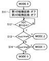
(1)出力電圧Voutがモード0の状態である場合
以下に、この場合におけるスイッチング電源10の制御方法について、図2を参照して説明する。図2は、モード0の場合におけるスイッチング電源10の制御方法を示すフローチャートである。
(1) When Output Voltage Vout is in
図2に示すように、判定回路24が、出力電圧Voutがモード0の状態である、と判定すると、その判定結果は、PWM回路26に送られる。
As shown in FIG. 2, when the
PWM回路26が上記判定結果を受け取ると、PWM回路26は、第1、第2の駆動回路27、28から第1、第2の制御パルスが出力されないように制御し、ハイサイドFET13、およびローサイドFET14を、共に非導通にする(S11)。
When the
この結果、コンデンサ17に充電された電力は、負荷12から放電される。コンデンサ17は大容量であるため、放電時間は長い。従って、長い期間、出力電圧Voutは、モード0の状態を維持する。しかしながら、コンデンサ17に充電された電力の放電によって、または負荷12が重負荷(インピーダンスが高い負荷)に切り替わることによって、出力電圧Voutは変動する。従って、以下の制御が必要となる。
As a result, the power charged in the capacitor 17 is discharged from the
次に、ADコンバータ21を制御することにより、ADコンバータ21は、出力電圧Voutの分圧Vdを一定時間毎にサンプリングしてデジタル値に変換し、このデジタル値を判定回路24に送る(ADC割り込みを行う)(S12)。
Next, by controlling the
次に、判定回路24が分圧Vdのデジタル値を受け取ると、判定回路24は、第2の基準値生成回路27から第2の基準電圧Vref2に基づいたデジタル値を読み出し、分圧Vdのデジタル値と、第2の基準電圧Vref2に基づくデジタル値と、を比較する。この両者のデジタル値を比較することによって、判定回路24は、出力電圧Voutが、第2の基準電圧Vref2より大きいか否かを判定する。(S13)。
Next, when the
判定回路24が分圧Vdのデジタル値を受け取らない場合には、判定回路24は、分圧Vdのデジタル値を受け取るまで上記判定動作を行わない。
When the
上記S13のステップによる判定の結果、判定回路24が、出力電圧Voutが第2の基準電圧Vref2より大きい、と判定した場合、スイッチグ電源10の制御方法を、モード2による制御方法に移行する。すなわち、判定回路24は、この判定結果をPWM回路26に送り、PMW回路26は、モード2による制御方法に基づいて、ハイサイドFET13およびローサイドFET14の動作を制御する。
If the
上記S13のステップによる判定の結果、判定回路24が、出力電圧Voutが第2の基準電圧Vref2以下であると判断した場合、判定回路24は、第1の基準値生成回路22から第1の基準電圧Vref1に基づくデジタル値を読み出し、電圧Vdのデジタル値と、第1の基準電圧Vref1に基づくデジタル値と、を比較する。この両者のデジタル値を比較することによって、判定回路24は、出力電圧Voutが、第1の基準電圧Vref1より小さいか否かを判定する。(S14)。
When the
上記S14のステップによる判定の結果、判定回路24が、出力電圧Voutが第1の基準電圧Vref1より小さいと判断した場合、スイッチグ電源10の制御方法を、モード1による制御方法に移行する。すなわち、判定回路24は、この判定結果をPWM回路26に送り、PMW回路26は、モード1による制御方法に基づいて、ハイサイドFET13およびローサイドFET14の動作を制御する。
If the
上記S14のステップによる判定の結果、判定回路24が、出力電圧Voutが第1の基準電圧Vref1以上であると判断した場合、スイッチング電源10の制御方法は、モード0による制御方法を維持する。すなわち、判定回路24は、この判定結果をPWM回路26に送り、PMW回路26は、モード0による制御方法に基づいて、ハイサイドFET13、およびローサイドFET14が、共に非導通の状態を維持するように、ハイサイドFET13およびローサイドFET14を制御する。
If the
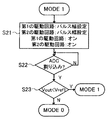
(2)出力電圧Voutがモード1の状態である場合
以下に、この場合におけるスイッチング電源10の制御方法について、図3および図4を参照して説明する。図3は、モード1の場合におけるスイッチング電源10の制御方法を示すフローチャートである。図4は、モード1の場合において、ハイサイドFET13およびローサイドFET14にそれぞれ供給される第1、第2の制御パルス、チョークコイル16を流れるインダクタンス電流IL、および出力電圧Voutの関係を示す波形図であり、同図(a)はハイサイドFET13に供給される第1の制御パルスの波形、同図(b)はローサイドFET14に供給される第2の制御パルスの波形、同図(c)はインダクタンス電流ILの波形、同図(d)は出力電圧Voutの波形を示す。
(2) When Output Voltage Vout is in
判定回路24が、出力電圧Voutがモード1の状態である、と判定すると、その判定結果をPWM回路26に送る。
When the
図3に示すように、PWM回路26が上記判定結果を受け取ると、PWM回路26は、第1の駆動回路27から出力される第1の制御パルスのパルス幅ton1およびパルス間隔と、第2の駆動回路28から出力される第2の制御パルスのパルス幅toff1´およびパルス間隔と、をそれぞれ算出する。その後、PWM回路26は、第1、第2の駆動回路27、28から、それぞれ所望の第1、第2の制御パルスを出力させ、ハイサイドFET13、およびローサイドFET14は、これらの制御パルスが入力されたときに導通状態になるように、スイッチング制御される。(S21)
なお、第1、第2の制御パルスは、図4(a)、(b)に示されるように、ハイサイドFET13およびローサイドFET14が同時に導通しないように、第1、第2の駆動回路27、28から出力される。
As shown in FIG. 3, when the
As shown in FIGS. 4A and 4B, the first and second control pulses are used so that the high-
ハイサイドFET13が導通されると、図4(c)に示されるように、一定期間だけチョークコイル16にインダクタンス電流ILが流れるため、コンデンサ17が充電される。従って、図4(d)に示されるように、出力電圧Voutが増加する。また、ローサイドFET14が導通されると、これが非導通の間にダイオード15に流れていたインダクタンス電流ILがローサイドFET14に流れる。従って、ダイオード15による電力消費は低減され、電源内部における電力の損失が抑制される。
When the high-
第1の制御パルスのパルス幅ton1は、以下のように算出される。 The pulse width ton1 of the first control pulse is calculated as follows.
ハイサイドFET13に第1の駆動回路27から第1の制御パルスが供給され、ハイサイドFET13が導通状態になると、チョークコイル16に、図1に示される矢印Iの方向を正方向として、正方向にインダクタンス電流LIが流れる。図4(c)に示すように、インダクタンス電流ILは、ゼロからピーク値Ipk1まで線形的に増加する。
When the first control pulse is supplied from the
インダクタンス電流ILのピーク値Ipk1は、入力源11から供給される電圧をVin、出力電圧をVout、第1の制御パルスのパルス幅をton1、およびチョークコイル16のインダクタンスをLとし、各素子の電圧降下0と仮定すると、式1のように表現される。
ハイサイドFET13に対して第1の制御パルスの供給が終了すると、ハイサイドFET13は、導通状態から非導通状態に切り替わり、図4(c)に示されるように、インダクタンス電流ILはIpk1から0まで低下する。ハイサイドFET13が非導通状態に切り替わってから、インダクタンス電流が0まで低下するまでの期間toff1は、式2より求められる。
図1に示される矢印Iの方向にインダクタンス電流ILが流れる期間(ton1+toff1)にコンデンサ17は充電され、出力電圧Voutは増加する。この間における出力電圧Voutの増加量ΔV1は、負荷12、第1の分圧抵抗19、および第2の分圧抵抗20に流れる電流を0とすると、コンデンサ17のキャパシタンスをCとし、式1、および式2を用いて、式3のように表現される。
このように、ΔV1が式4を満たすように第1の制御パルスのパルス幅ton1を設定すれば、一つの第1の制御パルスがハイサイドFET13に供給されることにより、出力電圧Voutを、Vref2−Vref1より小さい範囲で増加させることができる。従って、出力電圧Voutを増加させるために、ハイサイドFET13およびローサイドFET14をスイッチング動作させても、出力電圧Voutが第2の基準電圧Vref2を超えて大きくなることはない。
In this way, if the pulse width ton1 of the first control pulse is set so that ΔV1 satisfies Expression 4, one first control pulse is supplied to the high-
これに対して、第1の制御パルスのパルス幅を上述のように設定しない場合、出力電圧Voutが増加しすぎ、第2の基準電圧Vref2より大きく場合がある。この場合、モード2による制御によって、増加しすぎた出力電圧Voutを低下させる必要性が生じ、その分だけ無駄な電力が消費されるとともに、スイッチング電源10の応答速度も遅くなる。
On the other hand, when the pulse width of the first control pulse is not set as described above, the output voltage Vout may increase too much and be larger than the second reference voltage Vref2. In this case, it is necessary to reduce the output voltage Vout that has been increased excessively by the control in
なお、第1の制御パルスのパルス間隔は、式2に示されるtoff1より大きい範囲で適宜設定される。
Note that the pulse interval of the first control pulse is appropriately set in a range larger than toff1 shown in
また、第2の制御パルスのパルス幅toff1´は、式2に示されるtoff1より小さい範囲で適宜設定され、第2の制御パルスのパルス間隔は、第1の制御パルスのパルス間隔と同一となるように設定される。
Further, the pulse width toff1 ′ of the second control pulse is appropriately set within a range smaller than toff1 shown in
再び図3を参照する。ステップS21において、ハイサイドFET13およびローサイドFET14を、モード1による制御によって所望の動作を行わせる間に、ADコンバータ21を制御することにより、ADコンバータ21は、出力電圧Voutの分圧Vdを一定時間毎にサンプリングしてデジタル値に変換し、このデジタル値を判定回路24に送る(ADC割り込みを行う)(S22)。
Refer to FIG. 3 again. In step S21, the
次に、判定回路24が分圧Vdのデジタル値を受け取ると、判定回路24は、第1の基準値生成回路22から第1の基準電圧Vref1に基づくデジタル値を読み出し、分圧Vdのデジタル値と、第1の基準電圧Vref1に基づくデジタル値と、を比較する。この両者のデジタル値を比較することによって、判定回路24は、出力電圧Voutが、第1の基準電圧Vref1より小さいか否かを判定する。(S23)。
Next, when the
判定回路24が分圧Vdのデジタル値を受け取らない場合には、判定回路24は、分圧Vdのデジタル値を受け取るまで上記判定動作を行わない。
When the
上記S23のステップによる判定の結果、判定回路24が、出力電圧Voutが第1の基準電圧Vref1より小さいと判断した場合、スイッチング電源10の制御方法を、モード1のまま維持する。すなわち、判定回路24は、この判定結果をPWM回路26に送り、PMW回路26は、モード1による制御方法に基づいて、ハイサイドFET13およびローサイドFET14の動作を制御する。
If the
上記S23のステップによる判定の結果、判定回路20が、出力電圧Voutが第1の基準電圧Vref1以上であると判断した場合、スイッチング電源10の制御方法を、モード0による制御方法に移行させる。すなわち、判定回路24は、この判定結果をPWM回路26に送り、PMW回路26は、モード0による制御方法に基づいて、ハイサイドFET13およびローサイドFET14が共に非導通状態になるように、ハイサイドFET13およびローサイドFET14を制御する。
If the
以上に、モード1の場合におけるスイッチング電源10の制御方法を説明したが、モード1における制御方法において、判定回路24は、出力電圧Voutと第2の基準電圧Vref2との比較を行わない。これは、モード1において、一つの第1の制御パルスによって出力電圧Voutが上昇する量ΔV1は、Vref2−Vref1より小さい範囲であり、ハイサイドFET13をスイッチング動作させても、第2の基準電圧Vref2を超えて大きくなることはないからである。
Although the control method of the switching
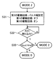
(3)出力電圧Voutがモード2の状態である場合
以下に、この場合におけるスイッチング電源10の制御方法について、図5および図6を参照して説明する。図5は、モード2の場合におけるスイッチング電源10の制御方法を示すフローチャートである。図6は、モード2の場合において、ハイサイドFET13およびローサイドFET14にそれぞれ供給される第1、第2の制御パルス、チョークコイル16を流れるインダクタンス電流IL、および出力電圧Voutの関係を示す波形図であり、同図(a)はハイサイドFET13に供給される第1の制御パルスの波形、同図(b)はローサイドFET14に供給される第2の制御パルスの波形、同図(c)はインダクタンス電流ILの波形、同図(d)は出力電圧Voutの波形を示す。
(3) When Output Voltage Vout is in
判定回路24が、出力電圧Voutがモード2の状態である、と判定すると、その判定結果をPWM回路26に送る。
When the
図5に示すように、PWM回路26が上記判定結果を受け取ると、PWM回路26は、図6(a)、(b)に示されるように、第2の駆動回路28から出力される第2の制御パルスのパルス幅toff2およびパルス間隔を算出する。その後、PWM回路26は、ハイサイドFET13が非導通になるように第1の駆動回路27を制御するととともに、ローサイドFET11がスイッチング動作するように第2の駆動回路28を制御する。(S31)
ローサイドFET14が導通されると、図6(c)に示されるように、ローサイドFET14が導通されている期間だけチョークコイル16に負方向にインダクタンス電流ILが流れ、コンデンサ17が放電される。従って、図6(d)に示されるように、出力電圧Voutが低下する。このように、コンデンサ17の放電は、負荷12だけではなく、ローサイドFET14を介して放電されるため、放電時間を早めることができ、スイッチング電源10の応答速度を速くすることができる。
As shown in FIG. 5, when the
When the low-
ここで、第2の制御パルスのパルス幅toff2は、以下のように算出される。 Here, the pulse width toff2 of the second control pulse is calculated as follows.
ローサイドFET14に第2の駆動回路28から第2の制御パルスが供給され、ローサイドFET14が導通状態になると、チョークコイル16に、負の方向にインダクタンス電流ILが流れる。図6(c)に示すように、インダクタンス電流ILは、ゼロからピーク値−Ipk2まで負方向に線形的に増加する。
When the second control pulse is supplied from the
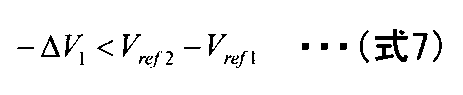
インダクタンス電流ILのピーク値−Ipk2は、出力電圧をVout、第2の制御パルスのパルス幅をtoff2、およびチョークコイル16のインダクタンスをLとし、各素子の電圧降下0と仮定すると、式5のように表現される。
負方向にインダクタンス電流ILが流れる期間(toff2)にコンデンサ17は放電し、出力電圧Voutは低下する。この間における出力電圧Voutの減少量−ΔV1は、負荷12、第1の分圧抵抗19、および第2の分圧抵抗20に流れる電流を0とすると、コンデンサ17のキャパシタンスをCとし、式5を用いて、式6のように表現される。
このように、−ΔV1が式7を満たすように第2の制御パルスのパルス幅toff2を設定すれば、一つの第2の制御パルスがローサイドFET14に供給されることにより、出力電圧Voutを、Vref2−Vref1より小さい範囲で低下させることができる。従って、出力電圧Voutを低下させるためにローサイドFET14をスイッチング動作させても、第1の基準電圧Vref1を超えて小さくなることはない。
In this way, if the pulse width toff2 of the second control pulse is set so that −ΔV1 satisfies Expression 7, one second control pulse is supplied to the low-
これに対して、第2の制御パルスのパルス幅を上述のように設定しない場合、出力電圧Voutが低下しすぎ、第1の基準電圧Vref1より小さく場合がある。この場合、モード1による制御によって、低下しすぎた出力電圧Voutを増加させる必要性が生じ、その分だけ無駄な電力が消費されるとともに、スイッチング電源10の応答速度も遅くなる。
On the other hand, when the pulse width of the second control pulse is not set as described above, the output voltage Vout may be too low and may be smaller than the first reference voltage Vref1. In this case, it becomes necessary to increase the output voltage Vout that has decreased too much due to the control in
なお、第2の制御パルスのパルス間隔は、チョークコイル16に連続的にインダクタンス電流ILが流れず、不連続的に流れる範囲で適宜設定される。
Note that the pulse interval of the second control pulse is appropriately set within a range in which the inductance current IL does not continuously flow through the
再び図5を参照する。ステップS31において、ローサイドFET14を、モード2による制御によって所望の動作を行わせる間に、ADコンバータ21を制御することにより、ADコンバータ21は、出力電圧Voutの分圧Vdを一定時間毎にサンプリングしてデジタル値に変換し、このデジタル値を判定回路24に送る(ADC割り込みを行う)(S32)。
Refer to FIG. 5 again. In step S31, the
次に、判定回路24が分圧Vdのデジタル値を受け取ると、判定回路24は、第2の基準値生成回路28から第2の基準電圧Vref2に基づくデジタル値を読み出し、分圧Vdのデジタル値と、第2の基準電圧Vref2に基づくデジタル値と、を比較する。この両者のデジタル値を比較することによって、判定回路24は、出力電圧Voutが、第2の基準電圧Vref2より大きいか否かを判定する。(S33)。
Next, when the
判定回路24が分圧Vdのデジタル値を受け取らない場合には、判定回路24は、分圧Vdのデジタル値を受け取るまで上記判定動作を行わない。
When the
上記S33のステップによる判定の結果、判定回路24が、出力電圧Voutが第2の基準電圧Vref1より大きいと判断した場合、スイッチング電源10の制御方法を、モード2のまま維持する。すなわち、判定回路24は、この判定結果をPWM回路26に送り、PMW回路26は、モード2による制御方法に基づいて、ハイサイドFET13およびローサイドFET14の動作を制御する。
If the
上記S33のステップによる判定の結果、判定回路24が、出力電圧Voutが第2の基準電圧Vref2以下であると判断した場合、スイッチング電源10の制御方法を、モード0による制御方法に移行させる。すなわち、判定回路24は、この判定結果をPWM回路26に送り、PMW回路26は、モード0による制御方法に基づいて、ハイサイドFET13およびローサイドFET14が共に非導通状態になるように、ハイサイドFET13およびローサイドFET14を制御する。
When the
以上に、モード2の場合におけるスイッチング電源10の制御方法を説明したが、モード2における制御方法において、判定回路24は、出力電圧Voutと第1の基準電圧Vref1との比較は行わない。これは、モード2において、一つの第2の制御パルスによって出力電圧Voutが減少する量は、Vref2−Vref1より小さい範囲であり、ローサイドFET14をスイッチング動作させても、第1の基準電圧Vref1を超えて小さくなることはないからである。
Although the control method of the switching
以上に、第1の実施形態にかかるスイッチング電源の制御方法を説明したが、図2、図3、および図5から明らかなように、各モードにおけるスイッチング電源10の制御方法は、複雑な計算を一切必要とすることがないため、スイッチング電源10を制御するための制御プログラムを簡素化できる。
The switching power supply control method according to the first embodiment has been described above. As is apparent from FIGS. 2, 3, and 5, the control method for the switching
また、上述のスイッチング電源10の制御方法はデジタル制御方式であるため、負荷12が無負荷、軽負荷から、チョークコイル16に連続的にインダクタンス電流ILが流れる程度の重負荷に切り替わる等して、出力電圧Voutが急激に低下しても、出力電圧Voutの急激な低下に対して直ちに応答することができる。
Further, since the control method of the switching
これに対して、上述のスイッチング電源10の制御方法と同様の制御を、演算増幅器を用いたアナログ制御方式で行う場合、出力電圧、すなわち演算増幅器に入力される電圧が急激に低下すると、出力電圧の低下に対して直ちに応答することができず、応答速度の遅れが発生する。これは、演算増幅器が、基準電圧と出力電圧が一致せず、演算増幅器が飽和すると、非飽和状態に切り替わるまでに長い時間を要する性質を有するためである。
On the other hand, when the same control method as the above-described control method for the switching
以上に説明した第1の実施形態に係る無負荷または軽負荷時におけるスイッチング電源10の制御方法およびスイッチング電源10によれば、モード2の場合に、ローサイドFET14をスイッチング動作させるため、コンデンサ17に充電された電力を、負荷12からだけでなく、ローサイドFET14を介して放電する。従って、放電時間を短くすることができ、スイッチング電源10の応答速度を速くすることができる。
According to the control method and the switching
さらに、第1の実施形態に係る無負荷または軽負荷時におけるスイッチング電源10の制御方法およびスイッチング電源10によれば、モード1の場合に、ローサイドFET14をスイッチング動作させるため、コンデンサ17の充電時において、ローサイドFET14が導通する期間は、ダイオード15に電流が流れず、ローサイドFET14に電流が流れる。従って、ダイオード15における電力消費が低減されるため、電力の内部損失を低減することができる。
Furthermore, according to the control method and the switching
(第2の実施形態)
図7は、第2の実施形態に係るスイッチング電源30を示す図である。このスイッチング電源30は、図1に示されるスイッチング電源30と比較して、電圧判定部31の構成が一部異なる。
(Second Embodiment)
FIG. 7 is a diagram illustrating a switching
図7に示されるスイッチング電源30の電圧判定部31は、第1の分圧抵抗19、第2の分圧抵抗20、第1のコンパレータ32、第2のコンパレータ33、第1の基準電圧Vref1に基づいた基準電圧Vref1´を出力する第1の基準電源34、第2の基準電圧Vref2に基づいた基準電圧Vref2´を出力する第2の基準電源35、および判定回路36を有する。これらのうち、第1の分圧抵抗19、および第2の分圧抵抗20については、図1に示されるスイッチング電源10と同様であるため、説明は省略する。
The
第1のコンパレータ32の一方の入力端子は、第1の分圧抵抗19と第2の分圧抵抗20との間に、並列に接続される。また、第1の基準電源34は、第1のコンパレータ32の他方の入力端子に接続される。
One input terminal of the
第1のコンパレータ32は、出力電圧Voutの分圧Vdが、基準電圧Vref1´より小さい場合に、分圧Vdと基準電圧Vref1´との差分電圧を出力するように接続される。
The
ここで、第1の分圧抵抗19の抵抗値をR1、第2の分圧抵抗20の抵抗値をR2とすれば、出力電圧Voutの分圧Vdは、Vd=(R2/R1+R2)Voutである。従って、基準電圧Vref1´を、第1の基準電圧Vref1に基づいて、Vref1´=(R2/R1+R2)Vref1と定めておけば、出力電圧Voutが第1の基準電圧Vref1より小さい場合、すなわち、モード1の場合に、第1のコンパレータ32は差分電圧を出力する。
Here, if the resistance value of the first
第2のコンパレータ33の一方の入力端子は、第1の分圧抵抗19と第2の分圧抵抗20との間に、第1のコンパレータ32と並列に接続される。また、第2の基準電源35は、第2のコンパレータ33の他方の入力端子に接続される。
One input terminal of the second comparator 33 is connected in parallel with the
第2のコンパレータ33は、出力電圧Voutの分圧Vdが、基準電圧Vref2´より大きい場合に、分圧Vdと基準電圧Vref2´との差分電圧を出力するように接続される。 The second comparator 33 is connected to output a differential voltage between the divided voltage Vd and the reference voltage Vref2 ′ when the divided voltage Vd of the output voltage Vout is larger than the reference voltage Vref2 ′.
ここで、出力電圧Voutの分圧Vdは、Vd=(R2/R1+R2)Voutであるため、基準電圧Vref2´を、第2の基準電圧Vref2に基づいて、Vref2´=(R2/R1+R2)Vref2と定めておけば、出力電圧Voutが第2の基準電圧Vref2より大きい場合、すなわち、モード2の場合に、第2のコンパレータ33は差分電圧を出力する。
Here, since the divided voltage Vd of the output voltage Vout is Vd = (R2 / R1 + R2) Vout, the reference voltage Vref2 ′ is expressed as Vref2 ′ = (R2 / R1 + R2) Vref2 based on the second reference voltage Vref2. If determined, when the output voltage Vout is higher than the second reference voltage Vref2, that is, in the
判定回路36は、第1のコンパレータ32、および第2のコンパレータ33のそれぞれの出力端子と、PWM回路26と、の間に配置され、それぞれに接続される。
The
以上に説明したスイッチング電源30は、同期整流方式の降圧型コンバータである。また、DC/DCコンバータの制御方式はアナログ制御方式である。
The switching
次に、第2の実施形態に係る無負荷または軽負荷時におけるスイッチング電源30の制御方法について説明する。この制御方法は、第1の実施形態に係るスイッチング電源10の制御方法と比較して、出力電圧Voutがモード0、モード1、モード2のいずれの状態であるかを判定する方法が異なる。以下に、出力電圧Voutの状態を判定する方法を説明する。
Next, a method for controlling the switching
出力端子に出力電圧Voutが発生すると、その分圧Vdは、第1のコンパレータ32、および第2のコンパレータ33にそれぞれ入力される。第1のコンパレータ32は、この分圧Vdと基準電圧Vref1´とを比較し、第2のコンパレータ33は、この分圧Vdと基準電圧Vref2´とを比較する。
When the output voltage Vout is generated at the output terminal, the divided voltage Vd is input to the
比較の結果、第1のコンパレータ32は、出力電圧Voutがモード1の場合に差分電圧を出力し、第2のコンパレータ33は、出力電圧Voutがモード2の場合に差分電圧を出力する。なお、出力電圧Voutがモード0の場合、第1のコンパレータ32、および第2のコンパレータ33は、それぞれ差分電圧を出力しない。
As a result of the comparison, the
このような比較結果は、判定回路36に入力される。判定回路36は、この比較結果に基づいて、出力電圧Voutが、モード0、モード1、モード2のいずれの状態であるかを判定する。
Such a comparison result is input to the
すなわち、判定回路36は、第1のコンパレータ32から差分電圧を受け取った場合に、出力電圧Voutがモード1であると判定し、第2のコンパレータ33から差分電圧を受け取った場合に、出力電圧Voutがモード2であると判定する。判定回路36は、両コンパレータ32、33から差分電圧を受け取らない場合、出力電圧Voutがモード0であると判定する。
That is, the
判定回路36によって、出力電圧Voutを判定した後のスイッチング電源30の制御方法については、第1の実施形態に係るスイッチング電源10の制御方法と同様である。
The method for controlling the switching
以上に説明した第2の実施形態に係る無負荷または軽負荷時におけるスイッチング電源30の制御方法およびスイッチング電源30であっても、モード1、モード2の各場合において適宜ローサイドFET14をスイッチング動作させるため、第1の実施形態に係るスイッチング電源10と同様の理由により、応答速度を向上させ、かつ電力の内部損失を低減することができる。
Even when the switching
(第3の実施形態)
図8は、第3の実施形態に係るスイッチング電源40を示す図である。図8に示すスイッチング電源40は、同期整流方式の昇圧型コンバータであって、制御方式はデジタル制御方式である。このスイッチング電源40は、電源本体が昇圧型の電源本体40−1(以下、電源本体40−1と称する)である点が、図1に示すスイッチング電源10と異なる。
(Third embodiment)
FIG. 8 is a diagram illustrating a switching
電源本体40−1は、図1に示す電源本体10−1を構成する各素子は同一であるが、これらの接続関係が異なっている。 The power supply main body 40-1 has the same elements as the power supply main body 10-1 shown in FIG.
チョークコイル16の一端は、入力源11に接続される。ダイオード15のアノードは、チョークコイル16の他端に接続され、ダイオード15のカソードは、コンデンサ17の一端に接続される。
One end of the
また、ハイサイドFET13のドレイン端子は、チョークコイル16の他端とダイオード15のアノードとの間に接続され、ハイサイドFET13のソース端子は、接地される。ローサイドFET14は、チョークコイル16の他端とコンデンサ17の一端との間に、ダイオード15と並列に接続される。ローサイドFET14のドレイン端子はチョークコイル16の他端に接続され、ローサイドFET14のソース端子はコンデンサ17の一端に接続される。
The drain terminal of the
このような電源本体40−1は、入力端子に入力源11が接続され、出力端子に負荷12が接続された状態で、ハイサイドFET13をスイッチング動作させると、入力源11から供給される電圧Vinを任意の出力電圧Voutに昇圧して、負荷12に供給する。
In such a power source main body 40-1, when the
このようなスイッチング電源40の無負荷または軽負荷時における制御方法は、第1の実施形態に係るスイッチング電源の制御方法と同様であり、モード1の場合には図4(a)(b)に示されるようにハイサイドFET13およびローサイドFET14をスイッチング動作させ、モード2の場合には図6(a)(b)に示されるようにローサイドFET14をスイッチング動作させる。
The control method of the switching
以上に説明した第3の実施形態に係る無負荷または軽負荷時におけるスイッチング電源40の制御方法およびスイッチング電源40であっても、モード1、モード2の各場合において適宜ローサイドFET14をスイッチング動作させるため、第1の実施形態に係るスイッチング電源10と同様の理由により、応答速度を向上させ、かつ電力の内部損失を低減することができる。
Even when the switching
(第4の実施形態)
図9は、第4の実施形態に係るスイッチング電源50を示す図である。図9に示すスイッチング電源50は、同期整流方式の反転型コンバータであって、制御方式はデジタル制御方式である。このスイッチング電源50は、電源本体が反転型の電源本体50−1(以下、電源本体50−1と称する)である点が、図1に示すスイッチング電源10と異なる。
(Fourth embodiment)
FIG. 9 is a diagram illustrating a switching
電源本体50−1は、図1に示す電源本体10−1を構成する各素子は同一であるが、これらの接続関係が異なっている。 The power supply main body 50-1 has the same elements as the power supply main body 10-1 shown in FIG.
チョークコイル16の一端は、ハイサイドFET13のソース端子に接続され、チョークコイル16の他端は、接地される。ダイオード15のカソードは、チョークコイル16の一端に接続され、ダイオード15のアノードは、コンデンサ17の一端に接続される。
One end of the
また、ローサイドFET14のドレイン端子は、チョークコイル16の一端とコンデンサ17の一端との間に、ダイオード15と並列に接続される。ローサイドFET14のドレイン端子はチョークコイル16の一端に接続され、ローサイドFET14のソース端子はコンデンサ17の一端に接続される。
The drain terminal of the low-
このような電源本体50−1は、入力端子に入力源11が接続され、出力端子に負荷12が接続された状態で、ハイサイドFET13をスイッチング動作させると、入力源11から供給される電圧Vinに対して極性が反転した電圧を出力電圧Voutとして、負荷12に供給する。
In such a power supply main body 50-1, when the
このようなスイッチング電源50の無負荷または軽負荷時における制御方法は、出力電圧Voutが第1の基準電圧Vref1より小さい場合(Vout<Vref1)に上述のモード2による制御を行い、出力電圧Voutが第2の基準電圧Vref2より大きい場合(Vout>Vref2)に上述のモード1による制御を行う他は、第1の実施形態に係るスイッチング電源10の制御方法と同様である。
Such a control method of the switching
以上に説明した無負荷または軽負荷時における反転型のスイッチング電源50の制御方法およびスイッチング電源50であっても、モード1、モード2の各場合において適宜ローサイドFET14をスイッチング動作させるため、第1の実施形態に係るスイッチング電源10と同様の理由により、応答速度を向上させ、かつ電力の内部損失を低減することができる。
Even in the control method and the switching
なお、図8、図9に示す各スイッチング電源40、50に対して、第2の実施形態に係るスイッチング電源30に適用された電圧判定部31を採用してもよく、このようなスイッチング電源であっても、本実施形態に係るスイッチング電源の効果が失われることはない。
Note that the
以上に、本発明の実施形態を説明したが、この実施形態は、例として提示したものであり、発明の範囲を限定することは意図していない。これらの新規な実施形態は、その他の様々な形態で実施されることが可能であり、発明の趣旨を逸脱しない範囲で、種々の省略、置き換え、変更を行うことができる。これらの実施形態やその変形は、発明の範囲や要旨に含まれるとともに、特許請求の範囲に記載された発明とその均等の範囲に含まれる。 Although the embodiment of the present invention has been described above, this embodiment is presented as an example and is not intended to limit the scope of the invention. These novel embodiments can be implemented in various other forms, and various omissions, replacements, and changes can be made without departing from the spirit of the invention. These embodiments and modifications thereof are included in the scope and gist of the invention, and are included in the invention described in the claims and the equivalents thereof.
10、30、40、50・・・スイッチング電源
10−1、40−1、50−1・・・電源本体
11・・・入力源
12・・・負荷
13・・・ハイサイドFET
14・・・ローサイドFET
15・・・ダイオード
16・・・チョークコイル
17・・・コンデンサ
18、31・・・電圧判定部
19・・・第1の分圧抵抗
20・・・第2の分圧抵抗
21・・・A/Dコンバータ
22・・・第1の基準値生成回路
23・・・第2の基準値生成回路
24、36・・・判定回路
25・・・スイッチ駆動部
26・・・パルス幅変調(PWM)回路
27・・・第1の駆動回路
28・・・第2の駆動回路
32・・・第1のコンパレータ
33・・・第2のコンパレータ
34・・・第1の基準電源
35・・・第2の基準電源
10, 30, 40, 50 ... switching power supply 10-1, 40-1, 50-1 ...
14 ... Low-side FET
DESCRIPTION OF
Claims (8)
前記スイッチング電源の出力電圧が、第1の基準電圧と、この電圧より大きい電圧である第2の基準電圧と、によって定められる基準電圧の範囲内であるか否かを判定するステップと、
このステップによる判定結果に基づいて、前記出力電圧が、前記基準電圧の範囲内になるように、前記第1のスイッチング素子および前記第2のスイッチング素子の動作を制御するステップと、
を具備し、
前記第1のスイッチング素子および前記第2のスイッチング素子を制御するステップは、前記出力電圧が前記第1の基準電圧より小さい場合は、前記第1のスイッチング素子の一度の導通によって増加する前記出力電圧の量が、前記第1の基準電圧と前記第2の基準電圧との差分電圧より小さくなるように、前記第1のスイッチング素子をスイッチングさせるとともに、前記第1のスイッチング素子と前記第2のスイッチング素子とが同時に導通せず、かつ前記インダクタンス素子に電流が流れているタイミングで前記第2のスイッチング素子が導通するように、前記第2のスイッチング素子をスイッチング動作させ、
前記出力電圧が前記第2の基準電圧より大きい場合は、前記第2のスイッチング素子の一度の導通によって減少する前記出力電圧の量が、前記差分電圧より小さくなるように、前記第2のスイッチング素子をスイッチングさせることを特徴とする無負荷または軽負荷時におけるスイッチング電源の制御方法。 A control method for a step-down or step-up switching power supply at the time of no load or light load having an inductance element, a diode, a capacitor, a first switching element, and a second switching element arranged in parallel with the diode. And
Determining whether the output voltage of the switching power supply is within a range of a reference voltage defined by a first reference voltage and a second reference voltage that is greater than this voltage;
Controlling the operations of the first switching element and the second switching element so that the output voltage falls within the range of the reference voltage based on the determination result of this step;
Comprising
The step of controlling the first switching element and the second switching element is performed when the output voltage is smaller than the first reference voltage, the output voltage increasing by one-time conduction of the first switching element. The first switching element and the second switching element are switched, and the first switching element and the second switching element are switched such that the amount of the first switching element is smaller than a differential voltage between the first reference voltage and the second reference voltage. Switching operation of the second switching element so that the second switching element is conductive at a timing when the element is not conductive at the same time and a current flows through the inductance element;
When the output voltage is greater than the second reference voltage, the second switching element is configured such that the amount of the output voltage that is reduced by one conduction of the second switching element is smaller than the differential voltage. Switching power supply control method at the time of no load or light load characterized by switching
前記スイッチング電源の出力電圧が、第1の基準電圧と、この電圧より大きい電圧である第2の基準電圧と、によって定められる基準電圧の範囲内であるか否かを判定するステップと、
このステップよる判定結果に基づいて、前記出力電圧が、前記基準電圧の範囲内になるように、前記第1のスイッチング素子および前記第2のスイッチング素子の動作を制御するステップと、
を具備し、
前記第1のスイッチング素子および前記第2のスイッチング素子を制御するステップは、前記出力電圧が前記第1の基準電圧より小さい場合は、前記第2のスイッチング素子の一度の導通によって増加する前記出力電圧の量が、前記差分電圧より小さくなるように、前記第2のスイッチング素子をスイッチングさせ、
前記出力電圧が前記第2の基準電圧より大きい場合は、前記第1のスイッチング素子の一度の導通によって減少する前記出力電圧の量が、前記第1の基準電圧と前記第2の基準電圧との差分電圧より小さくなるように、前記第1のスイッチング素子をスイッチングさせるとともに、前記第1のスイッチング素子と前記第2のスイッチング素子とが同時に導通せず、かつ前記インダクタンス素子に電流が流れているタイミングで前記第2のスイッチング素子が導通するように、前記第2のスイッチング素子をスイッチング動作させることを特徴とする無負荷または軽負荷時におけるスイッチング電源の制御方法。 An inversion type switching power supply control method at the time of no load or light load having an inductance element, a diode, a capacitor, a first switching element, and a second switching element arranged in parallel with the diode,
Determining whether the output voltage of the switching power supply is within a range of a reference voltage defined by a first reference voltage and a second reference voltage that is greater than this voltage;
Controlling the operations of the first switching element and the second switching element so that the output voltage falls within the range of the reference voltage based on the determination result of this step;
Comprising
The step of controlling the first switching element and the second switching element is performed when the output voltage is smaller than the first reference voltage, and the output voltage is increased by one conduction of the second switching element. The second switching element is switched so that the amount of is less than the differential voltage,
When the output voltage is greater than the second reference voltage, the amount of the output voltage that is decreased by one-time conduction of the first switching element is the difference between the first reference voltage and the second reference voltage. The timing at which the first switching element is switched so as to be smaller than the differential voltage, the first switching element and the second switching element are not simultaneously conducted, and a current flows through the inductance element. The switching power supply control method at the time of no load or light load, wherein the second switching element is switched so that the second switching element becomes conductive.
このステップにより算出されたパルス幅を有する前記第1の制御パルスを前記第1のスイッチング素子に供給し、若しくは前記算出ステップにより算出されたパルス幅を有する前記第2の制御パルスを前記第2のスイッチング素子に供給するステップと、
を具備し、
前記第1のスイッチング素子の導通時間は、前記第1の制御パルスのパルス幅によって制御されるとともに、前記第2のスイッチング素子の導通時間は、前記第2の制御パルスのパルス幅によって制御されることを特徴とする請求項1または2に記載の無負荷または軽負荷時におけるスイッチング電源の制御方法。 In the step of controlling the first switching element and the second switching element, the first switching element is set so that the output voltage falls within the range of the reference voltage based on a determination result in the determination step. Calculating a pulse width of a first pulse for controlling the operation of the element and a pulse width of a second pulse for controlling the operation of the second switching element;
The first control pulse having the pulse width calculated in this step is supplied to the first switching element, or the second control pulse having the pulse width calculated in the calculation step is supplied to the second switching pulse. Supplying the switching element;
Comprising
The conduction time of the first switching element is controlled by the pulse width of the first control pulse, and the conduction time of the second switching element is controlled by the pulse width of the second control pulse. 3. The method for controlling a switching power supply at the time of no load or light load according to claim 1 or 2.
このステップにより変換されたデジタル値と、前記第1の基準電圧に基づくデジタル値、および前記第2の基準電圧に基づくデジタル値とを比較することによって、前記出力電圧が、前記基準電圧の範囲内であるか否かを判定するステップと、
を具備することを特徴とする請求項1乃至3のいずれかに記載の無負荷または軽負荷時におけるスイッチング電源の制御方法。 The determining step includes converting a voltage obtained by dividing the output voltage into a digital value;
By comparing the digital value converted by this step with the digital value based on the first reference voltage and the digital value based on the second reference voltage, the output voltage falls within the range of the reference voltage. Determining whether or not
The method of controlling a switching power supply at the time of no load or light load according to any one of claims 1 to 3.
この電源本体の出力端子と前記コンデンサとの間に接続され、前記出力端子に発生した出力電圧が、第1の基準電圧と、この電圧より大きい電圧である第2の基準電圧と、によって定められる基準電圧の範囲内であるか否かを判定する電圧判定部と、
この電圧判定部に接続され、前記電圧判定部による判定結果に基づいて、前記出力電圧が、前記基準電圧の範囲内になるように、前記第1のスイッチング素子および前記第2のスイッチング素子の動作を制御するスイッチ駆動部と、
を具備し、
無負荷または軽負荷時における前記スイッチ駆動部は、前記出力電圧が前記第1の基準電圧より小さい場合は、前記第1のスイッチング素子の一度の導通によって増加する前記出力電圧の量が、前記第1の基準電圧と前記第2の基準電圧との差分電圧より小さくなるように、前記第1のスイッチング素子をスイッチング
させるとともに、前記第1のスイッチング素子と前記第2のスイッチング素子とが同時に導通せず、かつ前記インダクタンス素子に電流が流れているタイミングで前記第2のスイッチング素子が導通するように、前記第2のスイッチング素子をスイッチング動作させ、
前記出力電圧が前記第2の基準電圧より大きい場合は、前記第2のスイッチング素子の一度の導通によって減少する前記出力電圧の量が、前記差分電圧より小さくなるように、前記第2のスイッチング素子をスイッチングさせることを特徴とするスイッチング電源。 A step-down or step-up power supply body having an inductance element, a diode, a capacitor, a first switching element, and a second switching element arranged in parallel with the diode;
An output voltage that is connected between the output terminal of the power source body and the capacitor and that is generated at the output terminal is determined by a first reference voltage and a second reference voltage that is higher than the voltage. A voltage determination unit that determines whether the voltage is within a reference voltage range;
Operation of the first switching element and the second switching element is connected to the voltage determination unit, and based on the determination result by the voltage determination unit, the output voltage is within the range of the reference voltage. A switch driving unit for controlling
Comprising
When the output voltage is smaller than the first reference voltage, the switch driving unit at the time of no load or light load has an amount of the output voltage that is increased by one conduction of the first switching element. The first switching element is switched so that the difference voltage between the first reference voltage and the second reference voltage is smaller, and the first switching element and the second switching element are simultaneously turned on. And the switching operation of the second switching element so that the second switching element becomes conductive at a timing when a current flows through the inductance element,
When the output voltage is greater than the second reference voltage, the second switching element is configured such that the amount of the output voltage that is reduced by one conduction of the second switching element is smaller than the differential voltage. Switching power supply characterized by switching.
この電源本体の出力端子と前記コンデンサとの間に接続され、前記出力端子に発生した出力電圧が、第1の基準電圧と、この電圧より大きい電圧である第2の基準電圧と、によって定められる基準電圧の範囲内であるか否かを判定する電圧判定部と、
この電圧判定部に接続され、前記電圧判定部による判定結果に基づいて、前記出力電圧が、前記基準電圧の範囲内になるように、前記第1のスイッチング素子および前記第2のスイッチング素子の動作を制御するスイッチ駆動部と、
を具備し、
無負荷または軽負荷時における前記スイッチ駆動部は、前記出力電圧が前記第1の基準電圧より小さい場合は、前記第2のスイッチング素子の一度の導通によって増加する前記出力電圧の量が、前記差分電圧より小さくなるように、前記第2のスイッチング素子をスイッチングさせ、
前記出力電圧が前記第2の基準電圧より大きい場合は、前記第1のスイッチング素子の一度の導通によって減少する前記出力電圧の量が、前記第1の基準電圧と前記第2の基準電圧との差分電圧より小さくなるように、前記第1のスイッチング素子をスイッチングさせるとともに、前記第1のスイッチング素子と前記第2のスイッチング素子とが同時に導通せず、かつ前記インダクタンス素子に電流が
流れているタイミングで前記第2のスイッチング素子が導通するように、前記第2のスイッチング素子をスイッチング動作させることを特徴とするスイッチング電源。 An inverting power supply body having an inductance element, a diode, a capacitor, a first switching element, and a second switching element arranged in parallel with the diode;
An output voltage that is connected between the output terminal of the power source body and the capacitor and that is generated at the output terminal is determined by a first reference voltage and a second reference voltage that is higher than the voltage. A voltage determination unit that determines whether the voltage is within a reference voltage range;
Operation of the first switching element and the second switching element is connected to the voltage determination unit, and based on the determination result by the voltage determination unit, the output voltage is within the range of the reference voltage. A switch driving unit for controlling
Comprising
When the output voltage is smaller than the first reference voltage, the switch driving unit at the time of no load or light load has an amount of the output voltage that is increased by one conduction of the second switching element. Switching the second switching element to be smaller than the voltage;
When the output voltage is greater than the second reference voltage, the amount of the output voltage that is decreased by one-time conduction of the first switching element is the difference between the first reference voltage and the second reference voltage. The timing at which the first switching element is switched so as to be smaller than the differential voltage, the first switching element and the second switching element are not simultaneously conducted, and a current flows through the inductance element. A switching power supply, wherein the second switching element is switched so that the second switching element becomes conductive.
この回路および前記第1のスイッチング素子に接続され、前記第1の制御パルスを前記第1のスイッチング素子に供給する第1の駆動回路と、
前記パルス幅変調回路および前記第2のスイッチング素子に接続され、前記第2の制御パルスを前記第2のスイッチング素子に供給する第2の駆動回路と、
を具備し、
前記第1のスイッチング素子の導通時間は、前記第1の制御パルスのパルス幅によって制御されるとともに、前記第2のスイッチング素子の導通時間は、前記第2の制御パルスのパルス幅によって制御されることを特徴とする請求項5または6に記載のスイッチング電源。 The switch driver includes a pulse width of a first control pulse for controlling the operation of the first switching element, and a pulse width of a second control pulse for controlling the operation of the second switching element. A pulse width modulation circuit for calculating
A first drive circuit connected to the circuit and the first switching element and supplying the first control pulse to the first switching element;
A second drive circuit connected to the pulse width modulation circuit and the second switching element and supplying the second control pulse to the second switching element;
Comprising
The conduction time of the first switching element is controlled by the pulse width of the first control pulse, and the conduction time of the second switching element is controlled by the pulse width of the second control pulse. The switching power supply according to claim 5 or 6, wherein
前記第1の分圧抵抗と前記第2の分圧抵抗との間に接続され、前記第1、第2の分圧抵抗によって前記出力電圧を分圧した電圧を、デジタル値に変換するA/Dコンバータと、
前記第1の基準電圧に基づくデジタル値を出力する第1の基準値生成回路と、
前記第2の基準電圧に基づくデジタル値を出力する第2の基準値生成回路と、
前記A/Dコンバータ、第1の基準値生成回路、および第2の基準値生成回路、に接続され、前記A/Dコンバータによって変換されたデジタル値と、前記第1の基準電圧に基づくデジタル値および前記第2の基準電圧に基づくデジタル値とを比較することによって、前記出力電圧が、前記基準電圧の範囲内であるか否かを判定する判定回路と、
を具備することを特徴とする請求項5乃至7のいずれかに記載のスイッチング電源。 The voltage determination unit includes first and second voltage dividing resistors connected in series between the output terminal of the power source body and the capacitor,
An A / C connected between the first voltage dividing resistor and the second voltage dividing resistor, and converts the voltage obtained by dividing the output voltage by the first and second voltage dividing resistors into a digital value. A D converter,
A first reference value generation circuit that outputs a digital value based on the first reference voltage;
A second reference value generation circuit for outputting a digital value based on the second reference voltage;
A digital value connected to the A / D converter, a first reference value generation circuit, and a second reference value generation circuit and converted by the A / D converter, and a digital value based on the first reference voltage And a determination circuit that determines whether the output voltage is within a range of the reference voltage by comparing with a digital value based on the second reference voltage;
The switching power supply according to any one of claims 5 to 7, further comprising:
Priority Applications (1)
| Application Number | Priority Date | Filing Date | Title |
|---|---|---|---|
| JP2011069916A JP5550591B2 (en) | 2011-03-28 | 2011-03-28 | Switching power supply control method and switching power supply at light load or no load |
Applications Claiming Priority (1)
| Application Number | Priority Date | Filing Date | Title |
|---|---|---|---|
| JP2011069916A JP5550591B2 (en) | 2011-03-28 | 2011-03-28 | Switching power supply control method and switching power supply at light load or no load |
Publications (2)
| Publication Number | Publication Date |
|---|---|
| JP2012205455A true JP2012205455A (en) | 2012-10-22 |
| JP5550591B2 JP5550591B2 (en) | 2014-07-16 |
Family
ID=47185861
Family Applications (1)
| Application Number | Title | Priority Date | Filing Date |
|---|---|---|---|
| JP2011069916A Expired - Fee Related JP5550591B2 (en) | 2011-03-28 | 2011-03-28 | Switching power supply control method and switching power supply at light load or no load |
Country Status (1)
| Country | Link |
|---|---|
| JP (1) | JP5550591B2 (en) |
Citations (5)
| Publication number | Priority date | Publication date | Assignee | Title |
|---|---|---|---|---|
| JPH08331838A (en) * | 1995-06-01 | 1996-12-13 | Maxim Integrated Prod Inc | Method and apparatus for generating ouput voltage from inputvoltage supplied from input source |
| JPH11178329A (en) * | 1997-09-19 | 1999-07-02 | St Microelectron Srl | Current mode switching converter |
| JP2006254588A (en) * | 2005-03-10 | 2006-09-21 | Fujitsu Ltd | Control circuit and control method of current mode control type dc-dc convertor |
| JP2007116804A (en) * | 2005-10-19 | 2007-05-10 | Canon Inc | Switching power supply, electronic apparatus including the switching power supply, and control method of switching power supply |
| JP2010057222A (en) * | 2008-08-26 | 2010-03-11 | Toshiba Corp | Dc/dc converter |
-
2011
- 2011-03-28 JP JP2011069916A patent/JP5550591B2/en not_active Expired - Fee Related
Patent Citations (5)
| Publication number | Priority date | Publication date | Assignee | Title |
|---|---|---|---|---|
| JPH08331838A (en) * | 1995-06-01 | 1996-12-13 | Maxim Integrated Prod Inc | Method and apparatus for generating ouput voltage from inputvoltage supplied from input source |
| JPH11178329A (en) * | 1997-09-19 | 1999-07-02 | St Microelectron Srl | Current mode switching converter |
| JP2006254588A (en) * | 2005-03-10 | 2006-09-21 | Fujitsu Ltd | Control circuit and control method of current mode control type dc-dc convertor |
| JP2007116804A (en) * | 2005-10-19 | 2007-05-10 | Canon Inc | Switching power supply, electronic apparatus including the switching power supply, and control method of switching power supply |
| JP2010057222A (en) * | 2008-08-26 | 2010-03-11 | Toshiba Corp | Dc/dc converter |
Also Published As
| Publication number | Publication date |
|---|---|
| JP5550591B2 (en) | 2014-07-16 |
Similar Documents
| Publication | Publication Date | Title |
|---|---|---|
| JP5211959B2 (en) | DC-DC converter | |
| US8669748B2 (en) | Device for synchronous DC-DC conversion and synchronous DC-DC converter | |
| JP5195182B2 (en) | Current mode control switching regulator | |
| US8508208B2 (en) | Buck-boost regulator with converter bypass function | |
| KR101735440B1 (en) | System, method and apparatus to transition between pulse-width modulation and pulse-frequency modulation in a switch mode power supply | |
| US8624566B2 (en) | Current-mode control switching regulator and operations control method thereof | |
| JP4984777B2 (en) | Power supply system and output voltage control method | |
| JP4366335B2 (en) | Boost converter | |
| JP4631916B2 (en) | Boost DC-DC converter | |
| EP2973971B1 (en) | Systems and methods for 100 percent duty cycle in switching regulators | |
| JP3829753B2 (en) | DC-DC converter | |
| TW200917632A (en) | Comparator type DC-DC converter | |
| US9385603B2 (en) | Control method and control circuit for switching power supply | |
| JP2010259257A (en) | Switching regulator and operation control method thereof | |
| CN110875686B (en) | Electronic converter and method of operating an electronic converter | |
| JP4931092B2 (en) | Switching power supply, control circuit for controlling switching power supply, switching power supply control method, and module board | |
| JP4487649B2 (en) | Control device for step-up / step-down DC-DC converter | |
| US8344762B2 (en) | Gate driving circuit | |
| JP5428713B2 (en) | DC-DC converter and control method thereof | |
| US20170222557A1 (en) | Load capacitance determination circuitry and power supply control | |
| JP2019170073A (en) | Dcdc converter for vehicle | |
| JP2013172467A (en) | Switching power circuit | |
| JP7106769B2 (en) | Synchronous BUCK circuit control method, device, system and electronic device | |
| JP5550591B2 (en) | Switching power supply control method and switching power supply at light load or no load | |
| JP2009303347A (en) | Control circuit of dc-dc converter |
Legal Events
| Date | Code | Title | Description |
|---|---|---|---|
| A621 | Written request for application examination |
Free format text: JAPANESE INTERMEDIATE CODE: A621 Effective date: 20130125 |
|
| A977 | Report on retrieval |
Free format text: JAPANESE INTERMEDIATE CODE: A971007 Effective date: 20131219 |
|
| A131 | Notification of reasons for refusal |
Free format text: JAPANESE INTERMEDIATE CODE: A131 Effective date: 20140121 |
|
| A521 | Written amendment |
Free format text: JAPANESE INTERMEDIATE CODE: A523 Effective date: 20140130 |
|
| TRDD | Decision of grant or rejection written | ||
| A01 | Written decision to grant a patent or to grant a registration (utility model) |
Free format text: JAPANESE INTERMEDIATE CODE: A01 Effective date: 20140422 |
|
| A61 | First payment of annual fees (during grant procedure) |
Free format text: JAPANESE INTERMEDIATE CODE: A61 Effective date: 20140520 |
|
| R151 | Written notification of patent or utility model registration |
Ref document number: 5550591 Country of ref document: JP Free format text: JAPANESE INTERMEDIATE CODE: R151 |
|
| LAPS | Cancellation because of no payment of annual fees |