JP2012204961A - Antenna assembly - Google Patents
Antenna assembly Download PDFInfo
- Publication number
- JP2012204961A JP2012204961A JP2011065896A JP2011065896A JP2012204961A JP 2012204961 A JP2012204961 A JP 2012204961A JP 2011065896 A JP2011065896 A JP 2011065896A JP 2011065896 A JP2011065896 A JP 2011065896A JP 2012204961 A JP2012204961 A JP 2012204961A
- Authority
- JP
- Japan
- Prior art keywords
- capacitor
- conductive member
- bobbin
- antenna assembly
- connection terminal
- Prior art date
- Legal status (The legal status is an assumption and is not a legal conclusion. Google has not performed a legal analysis and makes no representation as to the accuracy of the status listed.)
- Pending
Links
Images


Abstract
Description
本発明は、コイルおよびコンデンサを備えるアンテナ組立体に関するものである。 The present invention relates to an antenna assembly including a coil and a capacitor.
昨今、無線を用いてドアやトランクのロック/アンロックを行うスマートキーシステムが主流になっている。アンテナ組立体としては、例えば特開2007−288345号公報(特許文献1)に記載されている。アンテナ組立体では、コイルとコンデンサが共振回路を構成している。アンテナ組立体のコンデンサは、コイルに電気的に接続された端子と、外部端子に電気的に接続された端子との上に載置され、各端子と接続および固定されている。 Recently, a smart key system that locks / unlocks doors and trunks using radio has become mainstream. As an antenna assembly, it describes in Unexamined-Japanese-Patent No. 2007-288345 (patent document 1), for example. In the antenna assembly, a coil and a capacitor constitute a resonance circuit. The capacitor of the antenna assembly is placed on a terminal electrically connected to the coil and a terminal electrically connected to the external terminal, and is connected and fixed to each terminal.
しかしながら、特許文献1の図5および図7に示されるように、コンデンサは、平坦な端子上に載置されて、安定して接続させるために接着剤等で各端子に固定される。つまり、コンデンサ載置時にはコンデンサが端子上で安定しない。これでは、作業者は、組付け作業において相当の神経を使わなければならない。また、組付けにおいてコンデンサが安定して載置できない以上、はんだ等の簡易な接着では足りず、別途接着剤等を用いて確実に固定しなければならなかった。
However, as shown in FIGS. 5 and 7 of
本発明は、このような事情に鑑みてなされたものであり、コンデンサを組付ける際に、コンデンサを安定して載置することができるアンテナ組立体を提供することを目的とする。 The present invention has been made in view of such circumstances, and an object of the present invention is to provide an antenna assembly capable of stably placing a capacitor when the capacitor is assembled.
上記課題を解決する請求項1に係るアンテナ組立体の発明は、ボビンと、前記ボビンに長手方向に沿って支持されたコアと、前記コアを巻回するコイルと、コンデンサと、各一端が前記ボビンの前端から長手方向に突出し、各他端が前記コイルおよび前記コンデンサの直列回路の各端部にそれぞれ接続された第一および第二コネクタ接続端子と、で一体的に組成されたアンテナ組立体と、前端側で開口し後端側に閉塞底面を有する有底穴が形成されたケースと、を備え、前記第一および第二コネクタ接続端子が前記開口側に位置するように前記アンテナ組立体が前記有底穴に挿入されて固定されたアンテナ組立体であって、前記ボビンに設けられ、一端が前記第一コネクタ接続端子に一体的に接続され、他端が前記コイルの一端に接続された第一導電部材が前記第一コネクタ接続端子側部と前記コイル側部とに所定間隔離して分割され、前記第一導電部材の前記分割された部分の第一コネクタ接続端子側端部および前記コイル側端部は、前記コンデンサの前記長手方向の長さに相当する距離だけ離れた位置でそれぞれ階段状又は凹状に屈曲されてコンデンサ段差部をなし、前記コンデンサは、前記コンデンサ段差部に載置された状態で各端子を前記第一コネクタ接続端子側端部および前記コイル側端部にそれぞれ接続され、一端が前記第二コネクタ接続端子に一体的に接続され、他端が前記コイルの他端に接続された第二導電部材が前記ボビンに設けられていることを特徴とする。
The invention of the antenna assembly according to
請求項2に係る発明は、請求項1において、前記第一導電部材、前記コンデンサ、および前記第二導電部材の上面を覆う前記ボビンの前端側部分には、前記第一導電部材の前記コンデンサ段差部を外部に露出させる空間部分が形成され、前記ボビンには、前記コンデンサに当接して前記コンデンサを前記長手方向および上下方向と直角な周方向に位置決めする周方向位置決め部が形成されていることを特徴とする。 According to a second aspect of the present invention, in the first aspect, the capacitor step of the first conductive member is provided on a front end side portion of the bobbin that covers the upper surfaces of the first conductive member, the capacitor, and the second conductive member. A space portion that exposes the portion to the outside is formed, and the bobbin has a circumferential positioning portion that contacts the capacitor and positions the capacitor in a circumferential direction perpendicular to the longitudinal direction and the vertical direction. It is characterized by.
請求項3に係る発明は、請求項2において、前記コンデンサ段差部の対面方向は、前記長手方向であり、前記位置決め部は、前記ボビンの空間部分を形成する側壁と一体に形成されていることを特徴とする。 According to a third aspect of the present invention, in the second aspect, the facing direction of the capacitor step portion is the longitudinal direction, and the positioning portion is formed integrally with a side wall that forms a space portion of the bobbin. It is characterized by.
請求項4に係る発明は、請求項1において、前記第一導電部材、前記コンデンサ、および前記第二導電部材の上面を覆う前記ボビンの前端側部分には、前記第一導電部材の前記コンデンサ段差部を外部に露出させる空間部分が形成され、前記コンデンサ段差部には、前記コンデンサに当接して前記コンデンサを前記長手方向および上下方向と直角な周方向に位置決めする周方向位置決め部が形成されていることを特徴とする。 According to a fourth aspect of the present invention, in the first aspect, the capacitor step of the first conductive member is disposed on a front end side portion of the bobbin that covers the upper surfaces of the first conductive member, the capacitor, and the second conductive member. A space portion that exposes the portion to the outside is formed, and a circumferential positioning portion that contacts the capacitor and positions the capacitor in a circumferential direction perpendicular to the longitudinal direction and the vertical direction is formed in the capacitor stepped portion. It is characterized by being.
請求項5に係る発明は、請求項2〜4の何れか一項において、前記第一コネクタ接続端子と前記第一導電部材の第一コネクタ接続端子側部は一体であり、前記第二コネクタ接続端子と前記第二導電部材は一体であり、前記ボビンは、前記第一および第二コネクタ接続端子が前記ボビンの前端から長手方向に突出する状態で前記第一導電部材と前記第二導電部材を内包してインサート成型されたことを特徴とするアンテナ組立体。 According to a fifth aspect of the present invention, in any one of the second to fourth aspects, the first connector connection terminal and the first connector connection terminal side portion of the first conductive member are integrated, and the second connector connection. The terminal and the second conductive member are integral, and the bobbin has the first conductive member and the second conductive member in a state where the first and second connector connecting terminals protrude in the longitudinal direction from the front end of the bobbin. An antenna assembly characterized by being enclosed and insert-molded.
請求項6に係る発明は、請求項2〜4の何れか一項において、前記第一コネクタ接続端子と前記第一導電部材の前記第一コネクタ接続端子側部は一体であり、前記第二コネクタ接続端子と前記第二導電部材は一体であり、前記ボビンは、前記第一導電部材の前記第一コネクタ接続端子側部と前記コイル側部とが第一連結部で連結され、かつ前記第二導電部材と前記第一連結部とが第二連結部で連結された状態で、前記第一および第二コネクタ接続端子が前記ボビンの前端から長手方向に突出するように前記第一導電部材および前記第二導電部材を内包してインサート成型され、前記空間部分は、前記第一導電部材の前記コンデンサ段差部、前記第一連結部および前記第二連結部を内在させる、前記ボビンに形成された貫通穴であり、前記第一連結部および前記第二連結部は前記インサート成型後にそれぞれ切断されていることを特徴とする。
The invention according to
請求項1の発明によれば、コンデンサ段差部により、コンデンサの位置規制が可能となり、コンデンサ組付け時に安定してコンデンサを載置することができる。これにより、例えば、コンデンサを接着剤等で固定することなく、各端子とはんだにて接続させることが可能となる。また、はんだを用いた場合、コンデンサ段差部により、はんだが安定しやすくなる。 According to the first aspect of the present invention, the capacitor step can be regulated by the capacitor step portion, and the capacitor can be stably placed when the capacitor is assembled. Thereby, for example, it is possible to connect each terminal with solder without fixing the capacitor with an adhesive or the like. Further, when solder is used, the solder is easily stabilized by the capacitor stepped portion.
請求項2の発明によれば、コンデンサは、ボビンの空間部分からコンデンサ段差部に載置されるとともに、位置決め部に当接する。これにより、さらに安定してコンデンサを載置することができる。
According to the invention of
請求項3の発明によれば、位置決め部として、ボビンの空間部分を構成する側壁自体または側壁と一体なものを用いることができ、より簡易な製造工程で請求項2の構成を実現することができる。
According to the invention of
請求項4の発明によれば、請求項2の発明同様、さらに安定してコンデンサを載置することができる。また、ボビンに位置決め部を形成する必要がなく、製造が容易となる。
According to the invention of
請求項5の発明によれば、インサート成型によって、アンテナ組立体を簡易に製造することができる。
According to the invention of
請求項6の発明によれば、第一連結部および第二連結部により一体となった第一導電部材および第二導電部材を、ボビンとインサート成型される。第一および第二導電部材は一体であるため、各端子の位置は位置決めされた状態である。したがって、第一および第二導電部材とボビンとを位置決めしてインサート成型するだけで、各端子同士および各端子とボビンの位置関係は正確となる。つまり、アンテナ組立体を簡易かつ正確に製造することができる。
According to invention of
次に、実施形態を挙げ、本発明をより詳しく説明する。
<第一実施形態>
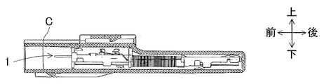
第一実施形態について図1〜6を参照して説明する。なお、図2は、各連結部614、624、74がつながっている状態(切断前)を表しているが、その他の部分は図1と同じである。また、図4は、コンデンサ段差部613、622の形状を説明するための模式図であって、点線は位置決め部22を表している。また、図6は、ケースのみ断面で表す。
Next, the present invention will be described in more detail with reference to embodiments.
<First embodiment>
A first embodiment will be described with reference to FIGS. Note that FIG. 2 shows a state in which the connecting
第一実施形態のアンテナ組立体1は、図1に示すように、ボビン2と、コア3と、コイル4と、コンデンサ5と、第一導電部材6と、第二導電部材7と、を備えている。
As shown in FIG. 1, the
ボビン2は、樹脂からなり、一方向に延伸した略直方体形状に形成されている。ここでは、ボビン2の長手方向を前後方向とする。また、前後方向および図1紙面に直交する方向を上下方向(図1手前が上方)とし、前後方向および上下方向に直交する方向を左右方向(図1上方が左方)とする。ボビン2の前端部には、ボビン2を上下方向に貫通した貫通穴21(空間部分)が形成されている。ボビン2の詳細は後述する。
The
コア3は、棒状の磁性体であって、ボビン2に長手方向に沿って支持されている。コイル4は、貫通穴21よりも後方であるボビン2の長手方向略中央で、コア3に巻回されている。コンデンサ5は、貫通穴21内部に配置され、コイル4と電気的に直列接続されており、コイル4とで共振回路を構成する。
The
第一導電部材6は、導体であって、それぞれ離間した、コネクタ側部位61と、コイル側部位62と、からなっている。つまり、第一導電部材6は、第一コネクタ接続端子612側の部位であるコネクタ側部位61と、コイル4側の部位であるコイル側部位62とに所定間隔離して分割されている。
The first
コネクタ側部位61(「第一コネクタ接続端子側部」に相当する)は、本体部611と、第一コネクタ接続端子612と、コンデンサ段差部613と、連結部614と、を有している。
The connector side portion 61 (corresponding to “first connector connection terminal side portion”) has a
本体部611は、平板形状であり、ボビン2内の前端部右側に前後方向に延伸して配置されている。本体部611は、前端がボビン2の前端位置に配置され、後端が貫通穴21内の右側面付近に配置されている。
The
第一コネクタ接続端子612は、本体部611の前端と一体に接続され、本体部611の前端から前方に延伸している。第一コネクタ接続端子612は、ボビン2の前端面から前方に突出している。第一コネクタ接続端子612は、外部コネクタ(図示せず)のコネクタ端子に接続される。
The first
コンデンサ段差部613は、本体部611の後端と一体に接続され、本体部611の後端から後方に延伸している。コンデンサ段差部613は、貫通穴21内に位置し、外部に露出している。コンデンサ段差部613は、図3および図4に示すように、本体部611に対して階段状に下方に屈曲している。換言すると、コンデンサ段差部613は、本体部611に対して下方に凹んだ略L字形状(側面視)となっている。コンデンサ段差部613上には、コンデンサ5の一方端子が載置され、はんだにより接続固定されている。
The
連結部614(「第一連結部」に相当する)は、平板形状であって、本体部611の左端と一体に接続されて後方に延伸している。連結部614の先端は、貫通穴21内に位置している。
The connecting portion 614 (corresponding to a “first connecting portion”) has a flat plate shape and is integrally connected to the left end of the
コイル側部位62(「コイル側部」に相当する)は、本体部621と、コンデンサ段差部622と、第一接続部623と、連結部624と、を備えている。
The coil side portion 62 (corresponding to a “coil side portion”) includes a
本体部621は、平板形状であり、本体部611より後方において、ボビン2内の前端部右側に前後方向に延伸して配置されている。本体部611は、前端がコンデンサ段差部613の後方で貫通穴21内の右側面付近に配置され、後端がボビン2内に配置されている。
The
コンデンサ段差部622は、本体部621の前端と一体に接続され、本体部621の前端から前方に延伸している。コンデンサ段差部622は、貫通穴21内に位置し、外部に露出している。コンデンサ段差部622は、図3および図4に示すように、本体部621に対して階段状に下方に屈曲している。換言すると、コンデンサ段差部622は、本体部621に対して下方に凹んだ略L字形状(側面視)となっている。
The
コンデンサ段差部622の前端は、コンデンサ段差部613の後端に対向かつ隔離して配置されている。コンデンサ段差部622上には、コンデンサ5の他方端子が載置され、はんだにより接続固定されている。コンデンサ段差部613、622を構成する上下方向に延伸した段差形成面613a、622a(L字の側面)は、コンデンサ5の長さ(一方端子がある端部から他方端子がある端部までの長さ)に相当する距離だけ隔離して対向配置されている。段差形成面613a、622aの対面方向は、前後方向である。段差形成面613a、622aの離間距離は、コンデンサ5の長さよりも若干大きくなっている。
The front end of the
第一接続部623は、本体部621の後端に一体に接続され、本体部621の後端から上方に延伸している。第一接続部623は、上端部がボビン2の上面から上方に突出している。第一接続部623の上端部には、コイル4の一端部が巻き付けられている。
The
連結部624(「第一連結部」に相当する)は、平板形状であって、本体部621の左端と一体に接続されて前方に延伸している。連結部624の先端は、貫通穴21内において、連結部614の先端に対向かつ離間して配置されている。
The connecting portion 624 (corresponding to the “first connecting portion”) has a flat plate shape and is integrally connected to the left end of the
このように、第一導電部材6は、コンデンサ5を介して、第一コネクタ接続端子612とコイル4の一端部とを電気的に接続している。
Thus, the first
第二導電部材7は、導体であって、本体部71と、第二コネクタ接続端子72と、第二接続部73と、連結部74と、を備えている。
The second
本体部71は、平板形状であり、本体部611と並列に、ボビン2内の前端部左側に前後方向に延伸して配置されている。本体部71は、前端がボビン2の前端位置に配置され、後端が貫通穴21より後方のボビン2内に配置されている。
The
第二コネクタ接続端子72は、本体部71の前端と一体に接続され、本体部71の前端から前方に延伸している。第二コネクタ接続端子72は、第一コネクタ接続端子612と並列に、ボビン2の前端面から前方に突出している。第二コネクタ接続端子72は、外部コネクタ(図示せず)のコネクタ端子に接続される。
The second
第二接続部73は、本体部71の後端に一体に接続され、本体部71の後端から上方に延伸している。第二接続部73は、上端部がボビン2の上面から上方に突出している。第二接続部73の上端部には、コイル4の他端部が巻き付けられている。
The
連結部74(「第二連結部」に相当する)は、平板形状であって、本体部71の右端と一体に接続されて下方に延伸している。連結部74の先端は、貫通穴21内において、連結部614の先端および連結部624の先端近傍に離間して配置されている。
The connecting portion 74 (corresponding to the “second connecting portion”) has a flat plate shape and is integrally connected to the right end of the
第二導電部材7は、第二コネクタ接続端子72とコイル4の他端部とを電気的に接続している。第一導電部材6および第二導電部財7により、コイル4とコンデンサ5の直列共振回路が構成される。
The second
ここで、図1、図4および図5に示すように、ボビン2には、貫通穴21の右側面に位置決め部22が設けられている。位置決め部22は、平板形状であり、貫通穴21の右側面と一体に形成されている。位置決め部22は、貫通穴21内で右側面に沿って上下方向に延在し、貫通穴21の右側面よりも若干上方に突出してコンデンサ5上面とほぼ同じ高さに形成されている。位置決め部22は、コンデンサ5の側面に当接している。なお、貫通穴21の壁面上部は面取りされているが、位置決め部22は面取りされておらず、平板形状となっている。
Here, as shown in FIGS. 1, 4, and 5, the
第一実施形態によれば、コンデンサ5は、コンデンサ段差部613、622によって位置規制がなされる。具体的には、コンデンサ5は、コンデンサ段差部613、622によって、前後方向の移動および下方への移動が制限されている。つまり、コンデンサ5は、上下方向および前後方向に位置決めされる。これにより、コンデンサ5を第一導電部材6に組付ける際、作業者(作業ロボットを含む)は、コンデンサ5を安定して載置することができる。
According to the first embodiment, the position of the
さらに、第一実施形態によれば、位置決め部22がコンデンサ5の側面に当接して、コンデンサ5の右方への移動を規制している。つまり、位置決め部22は、コンデンサ5を左右方向(上下方向および前後方向に直交する方向)に位置決めする。これにより、作業者は、さらに安定してコンデンサ5を載置することができる。また、位置決め部22は、貫通穴21の側面を利用しているため、貫通穴21の形成とともに形成することができ製造が容易となる。
Furthermore, according to the first embodiment, the positioning
第一実施形態は、コンデンサ5を安定して載置できる構成であるため、コンデンサ5と第一導電部材6との接続をはんだで行うことができる。当該接続は、例えば、リフローはんだやレーザーはんだにて実現することができ、接着剤等による固定は不要である。
Since 1st embodiment is the structure which can mount the capacitor |
ここで、アンテナ組立体2の製造方法について説明する。まず、図2に示すように、第一導電部材6と第二導電部材7とが一体となっている導体Dを製造する。そして、導体Dおよびコア3を含んだインサート成型により、ボビン2を導体Dおよびコア3と一体に製造する。ボビン2に貫通穴21を形成し、導体Dにおけるコンデンサ段差部613、622および連結部614、624、74を露出させる。そして、連結部614、624、74がそれぞれ隔離するように、上方から導体D(図2の斜線部分)を切断する。これにより、導体Dは、各端子が位置決めされた状態で、コネクタ側部位61と、コイル側部位62と、第二導電部材7とに分割される。
Here, a manufacturing method of the
続いて、コンデンサ5をコンデンサ段差部613、622上に載置する。このとき、コンデンサ5の側面を位置決め部22に当接させる。そして、リフローはんだまたはレーザーはんだにより、コンデンサ5の一方端子とコンデンサ段差部613とを接続固定し、コンデンサ5の他方端子とコンデンサ段差部622とを接続固定する。その後、コイル4をコア3に巻回し、各端部を第一および第二接続部623、73にそれぞれ巻き付ける。
Subsequently, the
つまり、アンテナ組立体1は、ボビン2が、コネクタ側部位61とコイル側部位62とが連結部614、624で連結され、かつ第二導電部材7と連結部614、624とが連結部74で連結された状態で、第一および第二コネクタ接続端子612、72がボビン2の前端から前方に突出するように導体Dを内包してインサート成型され、連結部614、622および連結部74がインサート成型後にそれぞれ切断されて製造させている。この製法によれば、各端子の位置決めが確実に行われた状態で、アンテナ組立体1を製造することができる。
That is, in the
なお、図6に示すように、アンテナ組立体2は、ケースCに挿入されてアンテナ装置を形成し、車両等に設置される。また、位置決め部22は、貫通穴21の側面に限らず、ボビン2の他の部位と一体に形成するものでもよい。また、位置決め部22は、貫通穴21の側面から内側(本実施形態では左側)に突出させて形成してもよい。また、位置決め部22は、貫通穴21の側面と同じ高さであってもよい。また、コンデンサ段差部613、622等の外部への露出は貫通穴21に限らず、上部のみが開口した貫通していないもの(空間部分)であってもよい。
As shown in FIG. 6, the
<第二実施形態>
第二実施形態について、図7を参照して説明する。第二実施形態のアンテナ組立体は、第一実施形態と比べて本体部611、621、コンデンサ段差部および位置決め部が異なり、他の構成は同じである。
<Second embodiment>
A second embodiment will be described with reference to FIG. The antenna assembly of the second embodiment is different from the first embodiment in the
第二実施形態のコンデンサ段差部8、9は、第一実施形態同様、コンデンサ5の長さに相当する距離離れて対向する段差形成面81、91を備えている。つまり、コンデンサ段差部8、9は、コンデンサ5の長さに相当する距離だけ離れた位置で対向するように階段状に下方に屈曲されている。
Similar to the first embodiment, the
ここで、第二実施形態において、本体部611、621の左右方向の幅は、コンデンサ5の左右方向の幅よりも大きい。コンデンサ段差部8、9は、本体部611、621の端部中央に一体に設けられている。つまり、コンデンサ段差部8、9の段差形成面81、91は、コンデンサ5の左右の幅に相当する距離だけ延在している。換言すると、コンデンサ段差部8、9は、本体部611、621の端部中央から、コンデンサ5の幅に相当する幅を有するように突出している。本体部611、621の端部形状は略コの字型(平面視)となる。
Here, in the second embodiment, the width of the
コンデンサ段差部8は、段差形成面81と、段差形成面81端部から後方に延びる段差側面82、83(「位置決め部」に相当する)によって囲まれた凹形状に形成されている。同様に、コンデンサ段差部9は、段差形成面91と、段差形成面91端部から前方に延びる段差側面92、93(「位置決め部」に相当する)によって囲まれた凹形状に形成されている。
The
これにより、第一実施形態同様の効果が得られる。さらに、段差側面82、83、92、93がコンデンサ5の左右方向(上下方向および対面方向に直交する方向)の移動を規制するため、より安定してコンデンサ5を載置することができる。また、ボビン2に位置決め部を設けず、第一導電部材6を加工するだけで足りるため、製造が容易となる。
Thereby, the effect similar to 1st embodiment is acquired. Furthermore, since the step side surfaces 82, 83, 92, 93 regulate the movement of the
<第三実施形態>
第三実施形態について、図8〜図10を参照して説明する。第三実施形態のアンテナ組立体は、第一実施形態と比べて本体部611、621、コンデンサ段差部および位置決め部が異なり、他の構成は同じである。
<Third embodiment>
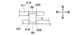
A third embodiment will be described with reference to FIGS. The antenna assembly of the third embodiment is different from the first embodiment in the
第三実施形態では、本体部611の後端部と本体部621の前端部は、左右に離間して並列するように配置されている。コンデンサ段差部8Aは、本体部611の後端部の右端と一体に形成されている。コンデンサ段差部9Aは、本体部621の前端部の左端と一体に形成されている。コンデンサ段差部8A(9A)は、第二実施形態同様、段差形成面81A(91A)と、段差側面82A、83A(92A、93A)とに囲まれた凹形状に形成されている。
In 3rd embodiment, the rear-end part of the main-
段差形成面81A、91Aの対面方向は左右方向となり、段差形成面81A、91Aの離間距離はコンデンサ5の長さに相当する。段差側面82A、83A(92A、93A)の離間距離は、コンデンサ5の幅(前後方向の長さ)に相当する。
The facing direction of the
これにより、第一実施形態同様の効果が発揮される。さらに、段差側面82A、83A(92A、93A)が位置決め部として機能し、第二実施形態同様の効果も発揮される。 Thereby, the effect similar to 1st embodiment is exhibited. Furthermore, the step side surfaces 82A and 83A (92A and 93A) function as positioning portions, and the same effects as those of the second embodiment are also exhibited.
なお、第三実施形態において、段差側面は、図9に示すように、各コンデンサ段差部8A(9A)に1面82A(93A)であってもよい。あるいは段差側面82A、83A(92A、93A)の離間距離は、コンデンサ5の幅よりも大きければよい。これらによっても、段差形成面81A、91Aにより少なくともコンデンサ5の左右方向の移動が規制され、安定して載置することができる。図9においては、コンデンサ段差部8Aの段差側面82Aとコンデンサ段差部9Aの段差側面93Aの前後方向の離間距離が、コンデンサ5の幅に相当するため、さらに安定して載置することができる。
In the third embodiment, the step side surface may be one
また、図10に示すように、コンデンサ段差部8B、9Bが本体部611、621の左右幅全体に設けられてもよい。この場合、段差形成面は、コンデンサ段差部8B(9B)における前後方向に対向する面81B、82B(91B、92B)となる。ここでは、段差形成面81B、82B(91B、92B)の離間距離は、コンデンサの幅(前後方向の長さ)に相当する。これによっても、段差形成面81B、82B(91B、92B)によりコンデンサ5の前後方向への移動が規制され、コンデンサ5を安定して載置することができる。
Further, as shown in FIG. 10,
1:アンテナ組立体、
2:ボビン、 21:貫通穴、 22:位置決め部、
3:コア、 4:コイル、 5:コンデンサ、
6:第一導電部材、
61:コネクタ側部位(第一コネクタ接続端子側部)、
611:本体部、 612:第一コネクタ接続端子、 613:コンデンサ段差部、 613a:段差形成面、 614:連結部(第一連結部)、
62:コイル側部位(コイル側部)、
621:本体部、 622:コンデンサ段差部、 622a:段差形成面、
623:第一接続部、 624:連結部(第一連結部)、
7:第二導電部材、
71:本体部、 72:第二コネクタ接続端子、 73:第二接続部、
74:連結部(第二連結部)、
8、8A、8B、9、9A、9B:コンデンサ段差部、
81A、81B、82B、91A、91B、92B:段差形成面、
82A、83A、92A、93A:段差側面(位置決め部)、
C:ケース、 D:導体
1: antenna assembly,
2: bobbin, 21: through hole, 22: positioning part,
3: Core, 4: Coil, 5: Capacitor,
6: first conductive member,
61: Connector side part (first connector connection terminal side part),
611: body portion, 612: first connector connection terminal, 613: capacitor step portion, 613a: step forming surface, 614: connecting portion (first connecting portion),
62: Coil side part (coil side part),
621: body portion, 622: capacitor step portion, 622a: step forming surface,
623: 1st connection part, 624: Connection part (1st connection part),
7: second conductive member,
71: Main body part 72: Second connector connection terminal 73: Second connection part
74: Connecting part (second connecting part),
8, 8A, 8B, 9, 9A, 9B: capacitor step portion,
81A, 81B, 82B, 91A, 91B, 92B: step forming surface,
82A, 83A, 92A, 93A: step side surface (positioning part),
C: Case, D: Conductor
Claims (6)
前記ボビンに設けられ、一端が前記第一コネクタ接続端子に一体的に接続され、他端が前記コイルの一端に接続された第一導電部材が前記第一コネクタ接続端子側部と前記コイル側部とに所定間隔離して分割され、
前記第一導電部材の前記分割された部分の第一コネクタ接続端子側端部および前記コイル側端部には、前記コンデンサの長さに相当する距離だけ離れた位置で対向するように階段状に屈曲されたコンデンサ段差部が設けられ、
前記コンデンサは、前記コンデンサ段差部に載置された状態で各端子を前記第一コネクタ接続端子側端部および前記コイル側端部にそれぞれ接続され、
一端が前記第二コネクタ接続端子に一体的に接続され、他端が前記コイルの他端に接続された第二導電部材が前記ボビンに設けられていることを特徴とするアンテナ組立体。 A bobbin, a core supported by the bobbin along the longitudinal direction, a coil that winds the core, a capacitor, and one end projecting from the front end of the bobbin in the longitudinal direction; An antenna assembly integrally composed of first and second connector connecting terminals respectively connected to each end of a series circuit of capacitors,
A first conductive member provided on the bobbin, having one end integrally connected to the first connector connecting terminal and the other end connected to one end of the coil includes the first connector connecting terminal side portion and the coil side portion. And divided into predetermined intervals,
The first connector connecting terminal side end and the coil side end of the divided portion of the first conductive member are stepped so as to face each other at a distance corresponding to the length of the capacitor. Bent capacitor step is provided,
The capacitor is connected to the first connector connection terminal side end and the coil side end in a state where the capacitor is placed on the capacitor stepped portion,
An antenna assembly, wherein a second conductive member having one end integrally connected to the second connector connecting terminal and the other end connected to the other end of the coil is provided on the bobbin.
前記第一導電部材、前記コンデンサ、および前記第二導電部材の上面を覆う前記ボビンの前端側部分には、前記第一導電部材の前記コンデンサ段差部を外部に露出させる空間部分が形成され、
前記ボビンには、前記コンデンサに当接して前記コンデンサを前記コンデンサ段差部の対面方向および上下方向と直角な方向に位置決めする位置決め部が形成されていることを特徴とするアンテナ組立体。 In claim 1,
The front end side portion of the bobbin that covers the top surfaces of the first conductive member, the capacitor, and the second conductive member is formed with a space portion that exposes the capacitor step portion of the first conductive member to the outside.
An antenna assembly according to claim 1, wherein the bobbin is formed with a positioning portion that contacts the capacitor and positions the capacitor in a direction perpendicular to the facing direction and the vertical direction of the capacitor stepped portion.
前記コンデンサ段差部の対面方向は、前記長手方向であり、
前記位置決め部は、前記ボビンの空間部分を形成する側壁と一体に形成されていることを特徴とするアンテナ組立体。 In claim 2,
The facing direction of the capacitor step portion is the longitudinal direction,
The antenna assembly according to claim 1, wherein the positioning portion is formed integrally with a side wall forming a space portion of the bobbin.
前記第一導電部材、前記コンデンサ、および前記第二導電部材の上面を覆う前記ボビンの前端側部分には、前記第一導電部材の前記コンデンサ段差部を外部に露出させる空間部分が形成され、
前記コンデンサ段差部には、前記コンデンサに当接して前記コンデンサを前記コンデンサ段差部の対面方向および上下方向と直角な方向に位置決めする位置決め部が形成されていることを特徴とするアンテナ組立体。 In claim 1,
The front end side portion of the bobbin that covers the top surfaces of the first conductive member, the capacitor, and the second conductive member is formed with a space portion that exposes the capacitor step portion of the first conductive member to the outside.
The antenna assembly according to claim 1, wherein the capacitor step portion is formed with a positioning portion that contacts the capacitor and positions the capacitor in a direction perpendicular to the facing direction and the vertical direction of the capacitor step portion.
前記第一コネクタ接続端子と前記第一導電部材の第一コネクタ接続端子側部は一体であり、前記第二コネクタ接続端子と前記第二導電部材は一体であり、
前記ボビンは、前記第一および第二コネクタ接続端子が前記ボビンの前端から長手方向に突出する状態で前記第一導電部材と前記第二導電部材を内包してインサート成型されたことを特徴とするアンテナ組立体。 In any one of Claims 2-4,
The first connector connection terminal and the first connector connection terminal side portion of the first conductive member are integral, and the second connector connection terminal and the second conductive member are integral,
The bobbin is insert-molded including the first conductive member and the second conductive member in a state where the first and second connector connection terminals protrude in the longitudinal direction from the front end of the bobbin. Antenna assembly.
前記第一コネクタ接続端子と前記第一導電部材の前記第一コネクタ接続端子側部は一体であり、前記第二コネクタ接続端子と前記第二導電部材は一体であり、
前記ボビンは、前記第一導電部材の前記第一コネクタ接続端子側部と前記コイル側部とが第一連結部で連結され、かつ前記第二導電部材と前記第一連結部とが第二連結部で連結された状態で、前記第一および第二コネクタ接続端子が前記ボビンの前端から長手方向に突出するように前記第一導電部材および前記第二導電部材を内包してインサート成型され、
前記空間部分は、前記第一導電部材の前記コンデンサ段差部、前記第一連結部および前記第二連結部を内在させる、前記ボビンに形成された貫通穴であり、
前記第一連結部および前記第二連結部は前記インサート成型後にそれぞれ切断されていることを特徴とするアンテナ組立体。 In any one of Claims 2-4,
The first connector connection terminal and the first connector connection terminal side portion of the first conductive member are integral, and the second connector connection terminal and the second conductive member are integral,
In the bobbin, the first connector connection terminal side part and the coil side part of the first conductive member are connected by a first connection part, and the second conductive member and the first connection part are second connection. In a state where the first and second connector connection terminals are connected at the part, the first conductive member and the second conductive member are included so as to protrude in the longitudinal direction from the front end of the bobbin, and insert molding is performed.
The space portion is a through-hole formed in the bobbin that includes the capacitor step portion, the first connection portion, and the second connection portion of the first conductive member,
The antenna assembly according to claim 1, wherein the first connecting portion and the second connecting portion are cut after the insert molding.
Priority Applications (1)
| Application Number | Priority Date | Filing Date | Title |
|---|---|---|---|
| JP2011065896A JP2012204961A (en) | 2011-03-24 | 2011-03-24 | Antenna assembly |
Applications Claiming Priority (1)
| Application Number | Priority Date | Filing Date | Title |
|---|---|---|---|
| JP2011065896A JP2012204961A (en) | 2011-03-24 | 2011-03-24 | Antenna assembly |
Publications (1)
| Publication Number | Publication Date |
|---|---|
| JP2012204961A true JP2012204961A (en) | 2012-10-22 |
Family
ID=47185490
Family Applications (1)
| Application Number | Title | Priority Date | Filing Date |
|---|---|---|---|
| JP2011065896A Pending JP2012204961A (en) | 2011-03-24 | 2011-03-24 | Antenna assembly |
Country Status (1)
| Country | Link |
|---|---|
| JP (1) | JP2012204961A (en) |
Cited By (4)
| Publication number | Priority date | Publication date | Assignee | Title |
|---|---|---|---|---|
| JP2013225947A (en) * | 2013-08-09 | 2013-10-31 | Sumida Corporation | Antenna coil component, antenna device and manufacturing method of antenna coil component |
| JP2015204557A (en) * | 2014-04-15 | 2015-11-16 | スミダコーポレーション株式会社 | Antenna device and method of manufacturing antenna device |
| CN107039769A (en) * | 2015-11-30 | 2017-08-11 | 胜美达集团株式会社 | A kind of manufacture method of antenna assembly and the antenna assembly |
| CN107257011A (en) * | 2013-08-09 | 2017-10-17 | 胜美达集团株式会社 | Aerial coil part |
Citations (5)
| Publication number | Priority date | Publication date | Assignee | Title |
|---|---|---|---|---|
| JPS6215899A (en) * | 1985-07-13 | 1987-01-24 | アルプス電気株式会社 | Manufacture of network electronic |
| JPH1117326A (en) * | 1997-06-24 | 1999-01-22 | Matsushita Electric Works Ltd | Method for soldering electronic parts |
| JP2004172527A (en) * | 2002-11-22 | 2004-06-17 | Rohm Co Ltd | Solid-state electrolytic capacitor and manufacturing method thereof |
| JP2008181947A (en) * | 2007-01-23 | 2008-08-07 | Sumida Corporation | Coil component for antenna |
| JP2010081088A (en) * | 2008-09-24 | 2010-04-08 | Sumida Corporation | Antenna for transmission |
-
2011
- 2011-03-24 JP JP2011065896A patent/JP2012204961A/en active Pending
Patent Citations (5)
| Publication number | Priority date | Publication date | Assignee | Title |
|---|---|---|---|---|
| JPS6215899A (en) * | 1985-07-13 | 1987-01-24 | アルプス電気株式会社 | Manufacture of network electronic |
| JPH1117326A (en) * | 1997-06-24 | 1999-01-22 | Matsushita Electric Works Ltd | Method for soldering electronic parts |
| JP2004172527A (en) * | 2002-11-22 | 2004-06-17 | Rohm Co Ltd | Solid-state electrolytic capacitor and manufacturing method thereof |
| JP2008181947A (en) * | 2007-01-23 | 2008-08-07 | Sumida Corporation | Coil component for antenna |
| JP2010081088A (en) * | 2008-09-24 | 2010-04-08 | Sumida Corporation | Antenna for transmission |
Cited By (7)
| Publication number | Priority date | Publication date | Assignee | Title |
|---|---|---|---|---|
| JP2013225947A (en) * | 2013-08-09 | 2013-10-31 | Sumida Corporation | Antenna coil component, antenna device and manufacturing method of antenna coil component |
| CN107257011A (en) * | 2013-08-09 | 2017-10-17 | 胜美达集团株式会社 | Aerial coil part |
| US10116053B2 (en) | 2013-08-09 | 2018-10-30 | Sumida Corporation | Antenna coil component, antenna unit, and method of manufacturing the antenna coil component |
| JP2015204557A (en) * | 2014-04-15 | 2015-11-16 | スミダコーポレーション株式会社 | Antenna device and method of manufacturing antenna device |
| CN107039769A (en) * | 2015-11-30 | 2017-08-11 | 胜美达集团株式会社 | A kind of manufacture method of antenna assembly and the antenna assembly |
| CN107039769B (en) * | 2015-11-30 | 2020-07-14 | 胜美达集团株式会社 | Antenna device and manufacturing method thereof |
| EP3174159B1 (en) * | 2015-11-30 | 2021-08-18 | Sumida Corporation | Antenna device and manufacturing method of antenna device |
Similar Documents
| Publication | Publication Date | Title |
|---|---|---|
| US10483646B2 (en) | Antenna device | |
| JP6418324B2 (en) | Multi-pole connector | |
| JP6390663B2 (en) | Electrical connector and manufacturing method thereof | |
| JP6663565B2 (en) | Board connector | |
| JP6152739B2 (en) | Noise filter device | |
| EP2184810A1 (en) | Board connector | |
| JP2010153476A (en) | Vertical coil component | |
| CN102437448B (en) | Coaxial connector plug | |
| US9263829B2 (en) | Durable plug connector assembly and method of assembling the same | |
| CN107039769B (en) | Antenna device and manufacturing method thereof | |
| US9871326B2 (en) | Connector with preformed metallic tubular mounting bracket | |
| JP5910682B2 (en) | Electrical connector | |
| JP2012204961A (en) | Antenna assembly | |
| KR20210151961A (en) | connector | |
| JP5517488B2 (en) | Board to board connector | |
| KR20210108471A (en) | coil parts | |
| JP6375681B2 (en) | Filter element built-in connector | |
| CN102656749B (en) | Electric connector assembly | |
| JP6238826B2 (en) | Surface mount connector | |
| WO2010052893A1 (en) | Electrical connector assembly | |
| JP2006216914A (en) | Electronic component housing | |
| CN102906945B (en) | Electrical connector assembly | |
| JP5725557B2 (en) | Connector and method for manufacturing outer shell of connector | |
| JP6547877B2 (en) | Antenna device | |
| US9379462B2 (en) | Cable connector and method of making the same |
Legal Events
| Date | Code | Title | Description |
|---|---|---|---|
| A621 | Written request for application examination |
Free format text: JAPANESE INTERMEDIATE CODE: A621 Effective date: 20140217 |
|
| A977 | Report on retrieval |
Free format text: JAPANESE INTERMEDIATE CODE: A971007 Effective date: 20140728 |
|
| A131 | Notification of reasons for refusal |
Free format text: JAPANESE INTERMEDIATE CODE: A131 Effective date: 20140930 |
|
| A02 | Decision of refusal |
Free format text: JAPANESE INTERMEDIATE CODE: A02 Effective date: 20150512 |