JP2012204524A - Solid state image pickup device - Google Patents
Solid state image pickup device Download PDFInfo
- Publication number
- JP2012204524A JP2012204524A JP2011066479A JP2011066479A JP2012204524A JP 2012204524 A JP2012204524 A JP 2012204524A JP 2011066479 A JP2011066479 A JP 2011066479A JP 2011066479 A JP2011066479 A JP 2011066479A JP 2012204524 A JP2012204524 A JP 2012204524A
- Authority
- JP
- Japan
- Prior art keywords
- semiconductor substrate
- main surface
- solid
- imaging device
- state imaging
- Prior art date
- Legal status (The legal status is an assumption and is not a legal conclusion. Google has not performed a legal analysis and makes no representation as to the accuracy of the status listed.)
- Withdrawn
Links
Images


Abstract
Description
本発明は、固体撮像装置に関し、特に、グローバル電子シャッター機能を有するMOS型固体撮像装置に関する。 The present invention relates to a solid-state imaging device, and more particularly to a MOS type solid-state imaging device having a global electronic shutter function.
固体撮像装置であるCCDイメージセンサやMOS型イメージセンサでは、多画素化に伴う画素サイズの微細化(微細セル化)が要求されている。それとともに、固体撮像装置に対しては、運動シーンなどの動きのある撮影においても、高い画質での撮像が可能な電気的な高速シャッター機能(グローバル電子シャッター機能)が求められている。特に、逐次読出し方式を採用するMOS型イメージセンサにおいても、全画素の受光部の信号電荷を電気的に一括して読み出すグローバル電子シャッター機能が求められている。 In CCD image sensors and MOS type image sensors that are solid-state imaging devices, pixel size miniaturization (miniaturization of cells) associated with the increase in the number of pixels is required. At the same time, a solid-state imaging device is required to have an electrical high-speed shutter function (global electronic shutter function) capable of capturing images with high image quality even in shooting with movement such as a motion scene. In particular, a MOS type image sensor that employs a sequential readout method is also required to have a global electronic shutter function that electrically reads out signal charges of light receiving portions of all pixels in a batch.
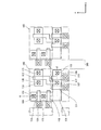
上記要望を受けて、種々の技術が提案されている(例えば、非特許文献1)。従来技術の一例として、非特許文献1で提案されている固体撮像装置(MOS型イメージセンサ)の構成および動作ポテンシャルについて、図18を用い説明する。
In response to the above request, various techniques have been proposed (for example, Non-Patent Document 1). As an example of the prior art, the configuration and operating potential of a solid-state imaging device (MOS type image sensor) proposed in Non-Patent
図18(a)の平面概略図に示すように、非特許文献1で提案されている固体撮像装置の各画素では、フォトダイオード903に対して、転送ゲート906を介してストレージダイオード904が設けられている。また、ストレージダイオード904に対して、転送ゲート907を介してフローティングディフュージョン905が設けられている。
As shown in the schematic plan view of FIG. 18A, in each pixel of the solid-state imaging device proposed in Non-Patent
また、フォトダイオード903に対しては、図18(a)の紙面に向かって上下方向において、転送ゲート913を介してオーバーフロードレイン911が設けられている。ここで、フォトダイオード903は、入射してきた光を電荷に変換する光電変換部として機能し、オーバーフロードレイン911は、フォトダイオード903で生成された電荷を一斉リセットして掃き出すための領域である。ストレージダイオード904は、一斉掃き出し後にフォトダイオード903から一斉読み出しされた信号電荷を一時蓄積するための領域である。
Further, an
次に、図18(a)におけるX−X’断面である図18(b)に示すように、非特許文献1で提案されている固体撮像装置では、オーバーフロードレイン911、フォトダイオード903、ストレージダイオード904、およびフローティングディフュージョン905の全てがp型ウェル領域902が形成された半導体基板901に埋め込み形成されており、フローティングディフュージョン905に対しては、リセットゲート908が設けられ、リセットゲート908には、ドレイン電圧909が設けられている。また、フローティングディフュージョン905に対しては、そのポテンシャル変化を増幅して外部に読み出す増幅器909が設けられている。
Next, as shown in FIG. 18B, which is a cross section taken along line XX ′ in FIG. 18A, in the solid-state imaging device proposed in Non-Patent
また、オーバーフロードレイン911には、ドレイン電圧912が設けられている。
次に、非特許文献1で提案されている固体撮像装置の駆動方法について、図18(c)を併せて用い説明する。図18(c)は、図18(a)におけるX−X’断面のポテンシャル図である。先ず、入射光によりフォトダイオード903に蓄積された電荷は、転送ゲート913を全画素一斉にONすることで、オーバーフロードレイン911へと掃き出される。これにより、全画素のフォトダイオード903が一斉にリセットされる(図18(c)における(i)PD−resetting)。
The
Next, a method for driving the solid-state imaging device proposed in
次に、リセットされて空になったフォトダイオード903に所定時間(シャッター時間)の入射光により蓄積された信号電荷は、転送ゲート906を全画素一斉にONすることで、ストレージダイオード906へと転送される。これにより、全画素のフォトダイオード903から信号電荷の一斉読み出しがなされる(図18(c)における(ii)First−transfer)。
Next, the signal charges accumulated by the incident light for a predetermined time (shutter time) in the
次に、ストレージダイオード904に転送された信号電荷は、MOS型イメージセンサの通常の読出し方式(逐次読み出し方式)のサイクルに従って、転送ゲート907をONすることで、フローティングディフュージョン905へと転送される(図18(c)における(iii)Second−transfer)。そして、フローティングディフュージョン905に接続された増幅器910を介して、フローティングディフュージョン905の信号電荷に応じたポテンシャル変化が外部へと読み出される。
Next, the signal charge transferred to the
上記のように、非特許文献1で提案されている固体撮像装置では、全画素において、フォトダイオード903の電荷をオーバーフロードレイン911へと一括リセットし、その後に、フォトダイオード903で所定時間(シャッター時間)の間で生成された信号電荷を全画素一斉に読み出してストレージダイオード904へと転送し、一時蓄積される。そして、ストレージダイオード904からフローティングディフュージョン905に転送された信号電荷に応じ、ポテンシャル変化が増幅器910を介して逐次読み出される。このようにして、グローバル電子シャッターが実現されている。
As described above, in the solid-state imaging device proposed in
しかしながら、上記非特許文献1で提案されている固体撮像装置では、単位画素において、半導体基板901内にフォトダイオード903とストレージダイオード904とが形成されており、フォトダイオード903の占有面積とストレージダイオード904の占有面積とは、トレードオフの関係となっている(図18(a)および図18(b)を参照)。そして、フォトダイオード903とストレージダイオード904の面積は、互いに同等とする必要があるため、フォトダイオード903の占有面積を相対的に大きくすることが困難であり、感度低下を招いてしまう。
However, in the solid-state imaging device proposed in
本発明は、上記問題の解決を図るべくなされたものであって、グローバル電子シャッター機能を備えながら、高い感度を有するMOS型の固体撮像装置を提供することを目的とする。 The present invention has been made to solve the above problems, and an object thereof is to provide a MOS type solid-state imaging device having high sensitivity while having a global electronic shutter function.
そこで、本発明では、次の構成を採用することとした。
[I] 本発明に係る固体撮像装置は、半導体基板と、光電変換部と、接続ダイオードと、蓄積ダイオードと、オーバーフロードレインとを有することを特徴とする。
Therefore, in the present invention, the following configuration is adopted.
[I] A solid-state imaging device according to the present invention includes a semiconductor substrate, a photoelectric conversion unit, a connection diode, a storage diode, and an overflow drain.
(1)光電変換部;半導体基板内における第1の主面側に、当該第1の主面に沿う状態で、且つ、互いの間に間隔をあけた状態で二次元形成されている。
(2)接続ダイオード;半導体基板内における第1の主面とは反対側の第2の主面側に、複数の光電変換部の各々に対応して設けられ、且つ、対応する光電変換部に接続されている。
(1) Photoelectric conversion unit: formed in a two-dimensional manner on the first main surface side in the semiconductor substrate in a state along the first main surface and with a space between each other.
(2) Connection diode; provided on the second main surface side opposite to the first main surface in the semiconductor substrate, corresponding to each of the plurality of photoelectric conversion units, and corresponding to the photoelectric conversion units It is connected.
(3)蓄積ダイオード;半導体基板内における前記第2の主面側に、接続ダイオードの各々に対応し、且つ、対応する接続ダイオードと第1ゲートを介して設けられている。
(4)オーバーフロードレイン;半導体基板内における第2の主面側に、接続ダイオードの各々に対応し、且つ、対応する接続ダイオードと第2ゲートを介して設けられている。
(3) Storage diode; provided on the second main surface side in the semiconductor substrate, corresponding to each of the connection diodes and via the corresponding connection diode and the first gate.
(4) Overflow drain; provided on the second main surface side in the semiconductor substrate, corresponding to each of the connection diodes and via the corresponding connection diode and the second gate.
[II] 本発明に係る固体撮像装置は、半導体基板と、光電変換部と、接続ダイオードと、蓄積ダイオードと、オーバーフロードレインとを有することを特徴とする。
(1)光電変換部;半導体基板内における第1の主面側に、当該第1の主面に沿う状態で、且つ、互いの間に間隔をあけた状態で二次元形成されている。
[II] A solid-state imaging device according to the present invention includes a semiconductor substrate, a photoelectric conversion unit, a connection diode, a storage diode, and an overflow drain.
(1) Photoelectric conversion unit: formed in a two-dimensional manner on the first main surface side in the semiconductor substrate in a state along the first main surface and with a space between each other.
(2)接続ダイオード;半導体基板内における第1の主面とは反対側の第2の主面側に、複数の光電変換部の各々に対応して設けられ、且つ、対応する光電変換部に接続されている。 (2) Connection diode; provided on the second main surface side opposite to the first main surface in the semiconductor substrate, corresponding to each of the plurality of photoelectric conversion units, and corresponding to the photoelectric conversion units It is connected.
(3)蓄積ダイオード;半導体基板内における第2の主面側に、接続ダイオードの各々に対応し、且つ、対応する接続ダイオードと第1ゲートを介して設けられている。
(4)オーバーフロードレイン;半導体基板内における第1の主面側に、隣接する光電変換部同士の間に設けられている。
(3) Storage diode; provided on the second main surface side in the semiconductor substrate, corresponding to each of the connection diodes and via the corresponding connection diode and the first gate.
(4) Overflow drain; provided on the first main surface side in the semiconductor substrate between adjacent photoelectric conversion portions.
先ず、[I]および[II]の双方の固体撮像装置では、半導体基板内の第1の主面側に光電変換膜が形成され、半導体基板内の第2の主面側に形成されたに蓄積ダイオードと占有面積という点においてトレードオフの関係にはない。このため、十分な受光部容量と十分な蓄積ダイオード容量との両立が可能である。よって、本発明に係る固体撮像装置では、グローバル電子シャッター機能を備える固体撮像装置において、画素サイズの微細化によっても、十分な光電変換部の面積を確保することができ、高い感度を実現することができる。 First, in both solid-state imaging devices [I] and [II], the photoelectric conversion film is formed on the first main surface side in the semiconductor substrate and is formed on the second main surface side in the semiconductor substrate. There is no trade-off between the storage diode and the occupied area. For this reason, it is possible to achieve both a sufficient light receiving unit capacitance and a sufficient storage diode capacitance. Therefore, in the solid-state imaging device according to the present invention, in a solid-state imaging device having a global electronic shutter function, a sufficient area of the photoelectric conversion unit can be ensured even by reducing the pixel size, and high sensitivity can be realized. Can do.
なお、[I]に係る本発明の固体撮像装置では、各画素において、接続ダイオードに対して第2ゲートを介してオーバーフロードレインが形成されている。このため、[I]に係る本発明の固体撮像装置では、全画素において、光電変換膜の電荷を下部電極、接続プラグ、および接続ダイオードを介して、オーバーフロードレインへと一括リセットし、その後に、光電変換膜で所定時間(シャッター時間)の間で生成された信号電荷を全画素一斉に読み出して蓄積ダイオードへと転送し、一時蓄積できる。そして、その後は、上記非特許文献1で提案されている固体撮像装置と同様に、蓄積ダイオードからフローティングディフュージョンに信号電荷が転送され、当該信号電荷に応じ、ポテンシャル変化が増幅器を介して逐次読み出される。このようにして、本発明に係る固体撮像装置においても、グローバル電子シャッター機能を備える。
In the solid-state imaging device of the present invention according to [I], in each pixel, an overflow drain is formed via a second gate with respect to the connection diode. Therefore, in the solid-state imaging device of the present invention according to [I], in all pixels, the charge of the photoelectric conversion film is collectively reset to the overflow drain via the lower electrode, the connection plug, and the connection diode, Signal charges generated during a predetermined time (shutter time) by the photoelectric conversion film can be read out all at once and transferred to a storage diode for temporary storage. Thereafter, similarly to the solid-state imaging device proposed in
一方、[II]に係る本発明の固体撮像装置では、オーバーフロードレインを半導体基板内の第2の主面側に形成するのではなく、半導体基板内の第1の主面側における隣接する光電変換部同士の間に形成している。このため、半導体基板内の第2の主面側にオーバーフロードレインを形成しない分、さらに蓄積ダイオードの占有面積を大きくとることができる。 On the other hand, in the solid-state imaging device of the present invention according to [II], the overflow drain is not formed on the second main surface side in the semiconductor substrate, but adjacent photoelectric conversion on the first main surface side in the semiconductor substrate. It is formed between the parts. For this reason, since the overflow drain is not formed on the second main surface side in the semiconductor substrate, the area occupied by the storage diode can be further increased.
以上のように、[I]および[II]の双方の本発明に係る固体撮像装置では、グローバル電子シャッター機能を備え、動きのある撮影においても、高い画質での撮像が可能である。従って、本発明に係る固体撮像装置では、グローバル電子シャッター機能を備えながら、高い感度を有する。 As described above, both [I] and [II] of the solid-state imaging device according to the present invention have a global electronic shutter function, and can capture images with high image quality even in moving shooting. Therefore, the solid-state imaging device according to the present invention has high sensitivity while having a global electronic shutter function.
本発明に係る固体撮像装置では、例えば、次のようなバリエーション構成を採用することが可能である。
上記本発明に係る固体撮像装置では、さらに、半導体基板内における第2の主面側に、蓄積ダイオードの各々に対応し、且つ、対応する蓄積ダイオードと第3ゲートを介して設けられたフローティングディフュージョンを有するという構成を採用することができる。このような構成を採用する場合には、各画素内において、蓄積ダイオードとフローティングディフュージョンを効率よく配置することができ、画素の微細化に際して有効である。
In the solid-state imaging device according to the present invention, for example, the following variation configuration can be adopted.
In the solid-state imaging device according to the present invention, the floating diffusion provided on the second main surface side in the semiconductor substrate corresponding to each of the storage diodes and provided via the corresponding storage diode and the third gate. It is possible to adopt a configuration having When such a configuration is adopted, the storage diode and the floating diffusion can be efficiently arranged in each pixel, which is effective for miniaturization of the pixel.
上記本発明に係る固体撮像装置では、半導体基板の第2の主面の上方において、隣接する光電変換部同士の間に相当する箇所には、遮光性を有する金属膜が形成されており、フローティングディフュージョンは、半導体基板における第1の主面側上方の少なくとも一部が、金属膜で覆われているという構成を採用することができる。このような構成を採用する場合には、隣接する光電変換部同士の間を通しての漏れ光を遮蔽することにより、漏れ光に起因するフローティングディフュージョンでの偽信号発生を抑制することができる。よって、高い画質性能を得られる。 In the solid-state imaging device according to the present invention, a light-shielding metal film is formed in a portion corresponding to between adjacent photoelectric conversion units above the second main surface of the semiconductor substrate, and is floating. The diffusion may employ a configuration in which at least a part of the semiconductor substrate at the upper part on the first main surface side is covered with a metal film. In the case of adopting such a configuration, it is possible to suppress the generation of a false signal in the floating diffusion caused by the leaked light by shielding the leaked light passing between the adjacent photoelectric conversion units. Therefore, high image quality performance can be obtained.
上記本発明に係る固体撮像装置では、半導体基板の前記第2の主面の上方において、隣接する光電変換部同士の間に相当する箇所には、遮光性を有する金属膜が形成されており、蓄積ダイオードは、半導体基板における第1の主面側上方の少なくとも一部が、金属膜で覆われているという構成を採用することができる。このような構成を採用する場合には、隣接する光電変換部同士の間を通しての漏れ光を遮蔽することにより、漏れ光に起因する蓄積ダイオードでの偽信号発生を抑制することができる。よって、高い画質性能を得られる。 In the solid-state imaging device according to the present invention, a light-shielding metal film is formed in a portion corresponding to between adjacent photoelectric conversion units above the second main surface of the semiconductor substrate, The storage diode can employ a configuration in which at least a part of the upper side of the first main surface of the semiconductor substrate is covered with a metal film. When such a configuration is employed, generation of a false signal in the storage diode due to the leaked light can be suppressed by shielding the leaked light passing between the adjacent photoelectric conversion units. Therefore, high image quality performance can be obtained.
上記[II]に係る本発明の固体撮像装置では、半導体基板の第2の主面の上方において、隣接する光電変換部同士の間に相当する箇所には、遮光性を有する金属膜が形成されており、オーバーフロードレインは、金属膜に接続されており、当該金属膜を介してバイアス電圧印加部からのバイアス電圧の印加を受けるという構成を採用することができる。このような構成を採用する場合には、金属膜にバイアス電圧を印加することにより、オーバーフロードレインの電荷状をリセットすることができ、グローバル電子シャッターを実現するのに有効である。 In the solid-state imaging device of the present invention according to [II] above, a light-shielding metal film is formed in a portion corresponding to between adjacent photoelectric conversion units above the second main surface of the semiconductor substrate. The overflow drain is connected to the metal film, and a configuration in which a bias voltage is applied from the bias voltage application unit via the metal film can be employed. When such a configuration is adopted, the charge state of the overflow drain can be reset by applying a bias voltage to the metal film, which is effective for realizing a global electronic shutter.
以下では、本発明を実施するための形態について、図面を参酌しながら説明する。なお、以下の各実施の形態は、本発明の構成およびそこから奏される作用・効果を分かり易く説明するために用いる例であって、本発明は、本質的な特徴部分以外に何ら以下の形態に限定を受けるものではない。 Hereinafter, embodiments for carrying out the present invention will be described with reference to the drawings. Each of the following embodiments is an example used for easily explaining the configuration of the present invention and the operations and effects produced therefrom, and the present invention is not limited to the following essential features. The form is not limited.
[実施の形態1]
1.固体撮像装置1の全体構成
実施の形態1に係る固体撮像装置1の全体構成について、図1を用い説明する。
[Embodiment 1]
1. Overall Configuration of Solid-
図1に示すように、実施の形態1に係る固体撮像装置1では、複数の画素部100がX−Y面方向にマトリクス状(行列状)に配列され、これより画素アレイ10が構成されている。画素アレイ10に対しては、パルス発生回路21、水平シフトレジスタ22、および垂直シフトレジスタ23が接続されている。水平シフトレジスタ22および垂直シフトレジスタ23は、パルス発生回路21からのタイミングパルスの印加に呼応して、各画素部100に対して、順次、駆動パルスを出力する。
As shown in FIG. 1, in the solid-
2.画素アレイ10の構成
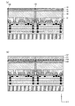
固体撮像装置1の構成の内、画素アレイ10の構成について、図2および図3を用い説明する。図2は、画素アレイ10における一部領域を抜き出して示す模式平面図であり、図3は、そのA−A‘断面、およびA−A’’断面を示す模式断面図であり、半導体基板表面側の読出し回路部の構造を示すA−A’断面と裏面フォトダイオード以降の上部(光入射側)の構造を示すA−A’’断面を組み合わせた模式図でり、構成部位の配置関係については、実際の配置とは異なっている。
2. Configuration of
図2に示すように、固体撮像装置1においては、フォトダイオード105が形成された領域(画素部)同士の間に画素分離部300が設けられている。そして、各画素部100には、接続ダイオード175、蓄積ダイオード106、フローティングディフュージョン107、増幅トランジスタ116、リセットドレイン108が設けられている。また、接続ダイオード175に対して、Y軸方向の上側には、オーバーフロードレイン109が設けられ、増幅トランジスタ116のX軸方向の右側には、増幅トランジスタ(Tr)ドレイン115が設けられている。
As shown in FIG. 2, in the solid-
接続ダイオード175と蓄積ダイオード106との間には、転送ゲート110が設けられ、接続ダイオード175とオーバーフロードレイン109との間には、転送ゲート114が設けられている。同様に、蓄積ダイオード106とフローティングディフュージョン107との間には、転送ゲート111が設けられ、フローティングディフュージョン107とリセットドレイン108との間には、転送ゲート113が設けられている。なお、増幅トランジスタ116の増幅Trゲート112は、ゲート酸化膜の開口117を介して、フローティングディフュージョン107に接続されている。
A
オーバーフロードレイン109およびリセットドレイン108には、それぞれコンタクトプラグ119,118が接続されており、また、増幅トランジスタ116には、コンタクトプラグ135が接続されている。また、転送ゲート114,110などには、それぞれコンタクトプラグ136が接続されている。
Contact plugs 119 and 118 are connected to the
ここで、蓄積ダイオード106およびフローティングディフュージョン107などは、隣接するフォトダイオード105同士の間の領域(画素分離部300)に配されている。
次に、固体撮像装置1の画素アレイ10の構成について、断面図にて説明する。
Here, the
Next, the configuration of the
図3に示すように、固体撮像装置1は、p型の半導体基板101を備え、図のZ軸方向下側の主面にゲート酸化膜104が積層形成されている。半導体基板101内における下側主面側の部分には、画素部100単位で、STI(Shallow Trench Isolation)102およびp+型のチャネルストッパ103が形成されている。
As shown in FIG. 3, the solid-
ゲート酸化膜104に対しては、Z軸方向下側に、層間絶縁膜120,121,122が順に積層形成されている。層間絶縁膜120,121,123は、例えば、CVD(Chemical Vapor Deposition)法を用い形成された酸化膜である。層間絶縁膜120における層間絶縁膜121との境界部分、および層間絶縁膜121における層間絶縁膜122との境界部分には、配線126,127がそれぞれ形成されている。配線126,127には、コンタクトプラグ123,124,125がそれぞれ接続されている。
For the
また、層間絶縁膜122に対しては、Z軸方向下側に、保護膜129が積層され、さらに、保護膜129のZ軸方向下側には、支持基板160が貼り合わされている。保護膜129における層間絶縁膜122との境界部分には、コンタクトプラグ125に接続された配線128が設けられている。
Further, a
配線126,127,128は、例えば、アルミニウム(Al)や銅(Cu)を用い形成されている。また、コンタクトプラグ123,124,125は、層間絶縁膜120,121,122に開けられたコンタクト孔に対して、タングステン(W)プラグを埋め込むことにより形成されているが、コンタクトプラグ123については、不純物層(リセットドレイン108、オーバーフロードレイン109)との接触抵抗低減のため、チタン(Ti)を、またタングステン(W)との密着を強化するためにTiNが、境界部分に介挿された構成を有する(図示を省略)。
The
半導体基板101におけるゲート絶縁膜104側の主面から内方に向けての表層領域には、画素部100毎に、オーバーフロードレイン109、接続ダイオード175、蓄積ダイオード106、フローティングディフュージョン107、およびリセットドレイン108が、互いに間隔をあけた状態で設けられている。オーバーフロードレイン109およびリセットドレイン108には、それぞれゲート酸化膜104を挿通するコンタクトプラグ123が接続されている。
In the surface layer region inward from the main surface on the
また、ゲート酸化膜104のZ軸方向下側には、接続ダイオード175とオーバーフロードレイン109との間の領域に転送ゲート114のゲート電極が設けられ、接続ダイオード175と蓄積ダイオード106との間の領域に転送ゲート110のゲート電極が設けられている。同様に、ゲート酸化膜104のZ軸方向下側には、蓄積ダイオード106とフローティングディフュージョン107との間の領域に転送ゲート111のゲート電極が設けられ、フローティングディフュージョン107とリセットドレイン108との間の領域に転送ゲート113のゲート電極が設けられている。
Further, on the lower side of the
さらに、フローティングディフュージョン107には、ゲート酸化膜104を挿通する増幅Trゲート112のゲート電極が接続されている。なお、図3では、転送ゲート110,111,113,114および増幅Trゲート112の各ゲート電極を黒色で示し、不純物拡散層間の対応する各箇所がゲートである。そして、転送ゲート110,111,113,114および増幅Trゲート112の各ゲート電極は、例えば、Poly−Siにより形成されている。
Further, the floating
なお、接続ダイオード175、蓄積ダイオード106、フローティングディフュージョン107、リセットドレイン108、およびオーバーフロードレイン109は、n型の不純物拡散層である。そして、図3に示すように、接続ダイオード175に対しては、ゲート酸化膜104との間の領域に、p+型の不純物層であるピニング層130が形成されている。これにより、接続ダイオード175は、埋め込みダイオードになっている。同様に、蓄積ダイオード106に対しては、ゲート酸化膜104との間の領域に、p+型の不純物層であるピニング層131が形成されている。これにより、蓄積ダイオード106についても、埋め込みダイオードになっている。
The
また、図示を省略しているが、リセットドレイン108には、ドレイン電圧(VDD)が接続されている。
一方、半導体基板101内のZ軸方向上側の表層部分には、画素部100毎にフォトダイオード105が形成されている。フォトダイオード105は、n型の不純物拡散層により構成されており、半導体基板101のZ軸方向上側の主面に沿ってマトリクス状に配されている。そして、フォトダイオード105は、各々が対応する接続ダイオード175に接続されている。
Although not shown, the
On the other hand, a
フォトダイオード105および半導体基板101のZ軸方向上側の面は、ピニング層140により全体が覆われており、その上に反射防止膜141および保護膜143が順に積層形成されている。そして、反射防止膜141の上の保護膜143との境界部分であって、各画素分離部300に対応する領域には、金属配線142が形成されている。金属配線142は、画素アレイ10を平面視する場合に、隣接する画素部100間を通るようにメッシュ状になっている。
The entire upper surface of the
保護膜143のZ軸方向上側には、平坦化膜150、カラーフィルタ層151、平坦化膜152、およびマイクロレンズ153が順に積層形成されている。この中で、カラーフィルタ層151は、画素部100毎に透過波長域が設定されている。
On the upper side of the
Z軸方向上方より入射した光は、画素部100毎にマイクロレンズ153で集光され、光電変換部としてのフォトダイオード105で光電変換される。そして、金属配線142が遮光性を有することから、入射した光が、半導体基板101に形成された各不純物拡散層(蓄積ダイオード106、フローティングディフュージョン107)に入射するのが防止される。
Light incident from above in the Z-axis direction is collected by the
なお、図3においては、固体撮像装置1の画素アレイ10の構成を説明するために、便宜上、蓄積ダイオード106やフローティングディフュージョン107のZ軸方向上方にフォトダイオード105が存在するように図示をしているが、実際には、図2に記載の配置関係を有する。
In FIG. 3, for the sake of convenience, in order to explain the configuration of the
3.固体撮像装置1の駆動
上記構成を有する固体撮像装置1は、グローバル電子シャッター機能を有するのであるが、その駆動について、図4から図6を用い説明する。
3. Driving of Solid-
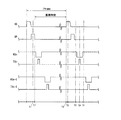
図4(a)は、本発明の実施の形態1に係る固体撮像装置1の内、一つの画素部100の等価回路であり、図4(b)は、各ノードのポテンシャルを示すポテンシャル図である。図5は、固体撮像装置1のグローバル電子シャッター動作のタイミングチャートの概略図であり、図6は、固体撮像装置1のグローバル電子シャッター動作時の画素部100の動作ポテンシャルの概略図である。
FIG. 4A is an equivalent circuit of one
図4(a)に示すように、フォトダイオード(PD)105には、転送ゲート(GR)114を介してオーバーフロードレイン(OFD)109が設けられ、また、転送ゲート(GS)110を介して蓄積ダイオード(SD)106が設けられている。 As shown in FIG. 4A, the photodiode (PD) 105 is provided with an overflow drain (OFD) 109 via a transfer gate (GR) 114 and stored via a transfer gate (GS) 110. A diode (SD) 106 is provided.
なお、図4(a)などでは、接続ダイオード175を省略している。
蓄積ダイオード(SD)106に対しては、転送ゲート(TX)111を介して、フローティングディフュージョン(FD)107が設けられている。そして、フローティングディフュージョン(FD)107は、増幅トランジスタ(SF)116のゲート(増幅Trゲート112)に接続され、また、転送ゲート(RS)113を介して、リセットドレイン(RD)108が設けられている。増幅トランジスタ(SF)のドレイン(SFD)115には、ドレイン電圧(VDD)が接続されている。
In FIG. 4A and the like, the
A floating diffusion (FD) 107 is provided for the storage diode (SD) 106 via a transfer gate (TX) 111. The floating diffusion (FD) 107 is connected to the gate (amplification Tr gate 112) of the amplification transistor (SF) 116, and a reset drain (RD) 108 is provided via the transfer gate (RS) 113. Yes. A drain voltage (V DD ) is connected to the drain (SFD) 115 of the amplification transistor (SF).
次に、図4(b)のポテンシャル図に示すように、各転送ゲート114,110,111,113において、ポテンシャルが低くなっており、他の各領域で高くなっている。
図5に示すように、転送パルスGSの印加開始タイミングから、次の転送パルスGSの印加開始までが1frameであり、転送パルスGRの印加が終了した直後から、次の転送パルスGSが印加開始されるまでの間が蓄積時間となる。
Next, as shown in the potential diagram of FIG. 4B, the potentials are low in the
As shown in FIG. 5, the period from the application start timing of the transfer pulse GS to the start of application of the next transfer pulse GS is 1 frame, and the application of the next transfer pulse GS is started immediately after the application of the transfer pulse GR is completed. The accumulation time is the time until
具体的に、図5に示すように、1frameの最初に、転送ゲート(GS)110のゲート電極に対して、全ての画素部100一括で転送パルスGSを印加する。これにより、フォトダイオード(PD)105に存在する電荷が、一斉に蓄積ダイオード(SD)106に転送される。
Specifically, as shown in FIG. 5, at the beginning of 1 frame, the transfer pulse GS is applied to the gate electrodes of the transfer gate (GS) 110 in a batch for all the
次に、転送ゲート(GR)114のゲート電極に対して、全ての画素部100一括でリセットパルスGRを印加する。これにより、フォトダイオード(PD)105の信号電荷が、一斉にオーバーフロードレイン(OFD)109に掃き出される(タイミングt1)。オーバーフロードレイン(OFD)109への電荷の掃き出しが行われた後、蓄積時間が開始される。
Next, a reset pulse GR is applied to all the
次に、n行目に位置する画素部100の転送ゲート(RS)113のゲート電極に対しては、リセットパルスRSnが印加され、これにより、n行目のフローティングディフュージョン(FD)107の電荷状態がリセットされる(タイミングt3)。次に、上記のように、転送ゲート(RS)113のゲート電極に対してリセットパルスRSnが印加されたn行目の画素部100に対しては、転送ゲート(TX)111のゲート電極に対して、転送パルスTXnが印加される。これにより、蓄積ダイオード(SD)106からフローティングディフュージョン(FD)107へと信号電荷が転送される(タイミングt4)。
Next, a reset pulse RS n is applied to the gate electrode of the transfer gate (RS) 113 of the
同様にして、(n+1)行目の画素部100における各転送ゲート(RS,TX)113,111のゲート電極に対して、リセットパルスRSn+1および転送パルスTXn+1がそれぞれ印加される。これにより、(n+1)行目の画素部100のフローティングディフュージョン(FD)107の電荷状態がリセットされ、蓄積ダイオード(SD)106からフローティングディフュージョン(FD)107へと信号電荷が転送される。
Similarly, the reset pulse RS n + 1 and the transfer pulse TX n + 1 are respectively applied to the gate electrodes of the transfer gates (RS, TX) 113 and 111 in the
なお、上記において、パルスGR,GSは、全画素部100に対して一斉に印加されるパルスであり、その他のパルスRSn,TXn,RSn+1,TXn+1,・・・は、逐次読み出し動作に従う各行単位に印加されるパルスである。
In the above description, the pulses GR and GS are pulses applied to all the
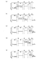
次に、図6(a)〜(e)の動作ポテンシャルの概略図を用いて、固体撮像装置1のグローバル電子シャッター動作を説明する。
ここで、図6(a)は、全画素部100のフォトダイオード(PD)105の電荷状態を一括リセット(受光部の信号電荷を一括リセット)した時(t=t1)の画素部100の動作ポテンシャルを示し、図6(b)は、全画素部100のフォトダイオード(PD)105の電荷状態を一括リセット後にフォトダイオード(PD)105に新たに蓄積された信号電荷を全画素部100一斉に蓄積ダイオード(SD)106に一括転送した時(t=t2)の画素部100の動作ポテンシャルを示す。
Next, the global electronic shutter operation of the solid-
Here, FIG. 6A shows the state of the
また、図6(c)は、n行目(ここでは、パルスTXn,RSnが印加される行)の蓄積ダイオード(SD)106の信号電荷をフローティングディフュージョン(FD)107に転送する前にフローティングディフュージョン(FD)107をリセットした時(t=t3)の画素部100の動作ポテンシャルを示し、図6(d)は、逐次読み出しのタイミングに従って、n行目の蓄積ダイオード(SD)106の信号電荷をフローティングディフュージョン(FD)107に転送した時(t=t4)の画素部100の動作ポテンシャルを示す。
Further, FIG. 6C illustrates a case where the signal charge of the storage diode (SD) 106 in the n-th row (here, the row to which the pulses TX n and RS n are applied) is transferred to the floating diffusion (FD) 107. FIG. 6D shows the operating potential of the
図6(e)は、(n+1)行目(ここでは、パルスTXn+1、RSn+1が印加される行)の蓄積ダイオード(SD)106の信号電荷をフローティングディフュージョン(FD)107に転送する前にフローティングディフュージョン(FD)107をリセットした時(t=t5)の画素部100の動作ポテンシャルを示す。
FIG. 6E shows a state before transferring the signal charge of the storage diode (SD) 106 in the (n + 1) th row (here, the row to which the pulses TX n + 1 and RS n + 1 are applied) to the floating diffusion (FD) 107. The operating potential of the
図6(a)に示すように、タイミングt1において、パルスGRの印加により(図5を参照)、転送ゲート(GR)114がONされる。これにより、全ての画素部100におけるフォトダイオード(PD)105に存在する電荷が一斉に、オーバーフロードレイン(OFD)109に転送され、掃出される。これにより、グローバル電子シャッターの読み出し(蓄積時間の開始)が開始される。
As shown in FIG. 6 (a), at time t 1, (see Figure 5) by applying a pulse GR, a transfer gate (GR) 114 is ON. As a result, the charges existing in the photodiodes (PD) 105 in all the
次に、図6(b)に示すように、タイミングt2において、パルスGSはONであり、パルスGRはOFFとなっている。そして、パルスTX(TXn,TXn+1,・・・)もOFFとなっている。パルスGSの印加により、転送ゲート(GS)110がONされ、全画素部100の転送ゲート(GS)110に一斉にパルスが印加されることにより、全画素部100のフォトダイオード(PD)105の信号電荷が一斉に、蓄積ダイオード(SD)106に転送され、一時蓄積される。そして、これによりグローバル電子シャッターの読み出しが終了(蓄積時間の終了)する。
Next, as shown in FIG. 6 (b), at timing t 2, the pulse GS is ON, the pulse GR is OFF. And the pulse TX (TX n , TX n + 1 ,...) Is also OFF. By applying the pulse GS, the transfer gate (GS) 110 is turned ON, and the pulses are applied to the transfer gates (GS) 110 of all the
また、パルスGRがOFFになった直後のタイミングt1’から、パルスGSがONになった直後のタイミングt2’までの蓄積時間が電子シャッター時間となり、任意の時間に設定することができる。 Further, the accumulation time from timing t 1 ′ immediately after the pulse GR is turned off to timing t 2 ′ immediately after the pulse GS is turned on is the electronic shutter time, and can be set to an arbitrary time.
次に、全画素部100一斉に蓄積ダイオード(SD)106に転送され、蓄積ダイオード(SD)106に蓄積されている信号電荷を、逐次読み出しでフローティングディフュージョン(FD)107を介して外部に読み出す説明に移る。
Next, all the
図6(c)に示すように、タイミングt3において、パルスGSおよびパルスGRはOFFとなっており、パルスRSnがON、パルスTXnがOFFである。この場合において、パルスRSnはON状態で、転送ゲート(RS)113のゲート電極に印加されることにより、フローティングディフュージョン(FD)107内の不要な電荷はリセットされ、リセット後の電位はドレイン電圧VDDとなる。 As shown in FIG. 6 (c), at time t 3, a pulse GS and pulse GR has become a OFF, pulse RS n is ON, the pulse TX n is turned OFF. In this case, the pulse RS n is in an ON state and is applied to the gate electrode of the transfer gate (RS) 113, whereby unnecessary charges in the floating diffusion (FD) 107 are reset, and the potential after the reset is the drain voltage. V DD .
次に、蓄積ダイオード(SD)106の信号電荷をフローティングディフュージョン(FD)107に転送する。
図6(d)に示すように、タイミングt4において、パルスGS,GRは、OFFであり、パルスTXnはON、パルスRSnはOFFである。この場合において、パルスTXnがONされ、転送ゲート(TX)111のゲート電極に印加されることにより、パルスTXnが印加される行の蓄積ダイオード(SD)106の電子シャッター後の信号電荷が、フローティングディフュージョン(FD)107に転送される。ここで、転送されてきた信号電荷の量に応じて、フローティングディフュージョン(FD)107の電位がVDDから変化する。この電位変化をソースフォロワーよりなる増幅トランジスタ(SF)116を介して映像信号として外部に読み出す。
Next, the signal charge of the storage diode (SD) 106 is transferred to the floating diffusion (FD) 107.
As shown in FIG. 6 (d), at time t 4, the pulse GS, GR is OFF, the pulse TX n ON, pulse RS n is OFF. In this case, when the pulse TX n is turned on and applied to the gate electrode of the transfer gate (TX) 111, the signal charge after the electronic shutter of the storage diode (SD) 106 in the row to which the pulse TX n is applied is changed. , And transferred to the floating diffusion (FD) 107. Here, the potential of the floating diffusion (FD) 107 changes from V DD in accordance with the amount of signal charge transferred. This potential change is read out to the outside as a video signal through an amplification transistor (SF) 116 formed of a source follower.
ここで、上記に示すように、蓄積ダイオード(SD)106の信号電荷をフローティングディフュージョン(FD)107に転送するタイミング以外の期間は、パルスRSnはON状態で、転送ゲート(RS)113のゲート電極に印加されることにより、フローティングディフュージョン(FD)107内の不要な電荷はリセットされ続けている。 Here, as shown above, a period other than the timing of transfer of the signal charge accumulation diode (SD) 106 to the floating diffusion (FD) 107, a pulse RS n In the ON state, the gate of the transfer gate (RS) 113 By being applied to the electrodes, unnecessary charges in the floating diffusion (FD) 107 continue to be reset.
次に、(n+1)行目における、蓄積ダイオード(SD)106に蓄積されている信号電荷の逐次読み出しに移る。
図6(e)に示すように、タイミングt5において、パルスGS,GRはOFFであり、パルスRSn+1はONであり、パルスTXn+1はOFFである。この場合において、パルスRSn+1がONされ、転送ゲート(RS)113のゲート電極に印加されることにより、フローティングディフュージョン(FD)107内の不要な電荷はリセットされ、リセット後の電位はドレイン電圧VDDとなる。これ以降は、図6(c)〜図6(e)の逐次読み出しの駆動のサイクルを全ての行を読み出すまで繰り返し、電子シャッター動作で任意の蓄積時間で撮像した画像の読み出しを終了する。
Next, in the (n + 1) th row, the process proceeds to sequential reading of signal charges accumulated in the storage diode (SD) 106.
As shown in FIG. 6 (e), at time t 5, a pulse GS, GR is OFF, the pulse RS n + 1 is ON, the pulse TX n + 1 is OFF. In this case, the pulse RS n + 1 is turned on and applied to the gate electrode of the transfer gate (RS) 113, so that unnecessary charges in the floating diffusion (FD) 107 are reset, and the potential after the reset is the drain voltage V It becomes DD . Thereafter, the sequential readout driving cycle shown in FIGS. 6C to 6E is repeated until all rows are read out, and the readout of the image captured in an arbitrary accumulation time by the electronic shutter operation is completed.
4.効果
本実施の形態に係る固体撮像装置1では、半導体基板101内の一方の主面側(図3のZ軸方向上側の主面側)にフォトダイオード105を有し、半導体基板101内の他方の主面側(図3のZ軸方向下側の主面側)に蓄積ダイオード106が形成されているため、フォトダイオード105と蓄積ダイオード106とが、占有面積という点において互いにトレードオフの関係にはない。このため、十分な受光部容量と十分な蓄積ダイオード106の容量との両立が可能である。よって、固体撮像装置1では、グローバル電子シャッター機能を備える固体撮像装置において、画素部100のサイズの微細化によっても、十分な光電変換部の面積を確保することができ、高感度で、大きなダイナミックレンジを実現することができる。
4). Effect In the solid-
また、固体撮像装置1では、各画素部100において、接続ダイオード175に対して転送ゲート114を介してオーバーフロードレイン109が形成されている。このため、固体撮像装置1では、全画素部100において、フォトダイオード105および接続ダイオード105の蓄積電荷をオーバーフロードレイン109を介して一括リセットし、その後に、フォトダイオード105で所定時間(シャッター時間)の間で生成された信号電荷を全画素部100一斉に読み出して蓄積ダイオード106へと転送し、一時蓄積できる。そして、その後は、上記のように、蓄積ダイオード106からフローティングディフュージョン107に信号電荷が転送され、当該信号電荷に応じてポテンシャル変化が増幅トランジスタ116を介して逐次読み出される。このようにして、本実施の形態に係る固体撮像装置1においても、グローバル電子シャッター機能を備える。
In the solid-
以上のように、本実施の形態に係る固体撮像装置1では、グローバル電子シャッター機能を備え、動きのある撮影においても、高い画質での撮像が可能であり、グローバル電子シャッター機能を備えながら、高い感度を有する。
As described above, the solid-
また、本実施の形態に係る固体撮像装置1では、画素分離部300に遮光性を有する金属配線142が形成されており、接続ダイオード175、蓄積ダイオード106およびフローティングディフュージョン107が、金属配線142の下方に形成されており、蓄積ダイオード106およびフローティングディフュージョン107が、金属配線142の下方に形成されている。このため、固体撮像装置1では、隣接するフォトダイオード105同士の間(画素分離部300)を通しての光の入射が防止され、接続ダイオード175、蓄積ダイオード106およびフローティングディフュージョン107での偽信号電荷の発生を防止することができ、これに起因する画質の劣化を防止することができる。よって、本実施の形態に係る固体撮像装置1では、偽信号電荷の混入が生じることがなく、高い画質を得ることができる。
In the solid-
5.固体撮像装置1の製造方法
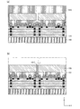
本実施の形態に係る固体撮像装置1の製造方法について、図7から図9を用い説明する。
5. Manufacturing Method of Solid-State Imaging Device 1 A manufacturing method of the solid-
図7(a)に示すように、半導体基板1010に対して、リソグラフィー用のアライメントマークを形成し(図示を省略)、その後にn+型の不純物拡散層であるフォトダイオード105を画素部100毎に形成する。フォトダイオード105は、例えば、リン(P)や砒素(As)を、300[keV]〜500[keV]、1×10¹²[cm−2]〜1×10¹³[cm−2]で、イオン注入することにより形成される。
As shown in FIG. 7A, an alignment mark for lithography is formed on a semiconductor substrate 1010 (not shown), and then a
次に、トランジスタや拡散層の素子を分離するSTI(Shallow Trench Isolatio)102を形成する。具体的には、半導体基板1010の該当箇所をドライエッチングすることで、例えば、分離領域となる深さ200[nm]〜400[nm]の溝を形成する。次に、形成した溝と半導体基板1010の界面の欠陥領域を低減するため、熱酸化等により、例えば、酸化膜厚10[nm]〜20[nm]の犠牲酸化を行い、さらに、例えば10[keV]〜20[keV]、1×10¹³[cm−2]〜3×10¹³[cm−2]で、ホウ素(B)のイオン注入を行い、P+層のチャネルストッパ103を形成する。
Next, an STI (Shallow Trench Isolation) 102 for separating transistors and diffusion layer elements is formed. Specifically, by performing dry etching on a corresponding portion of the
次に、熱酸化、またはプラズマ酸化等により、例えば、膜厚5[nm]〜10[nm]のゲート酸化膜1040を形成する。ゲート酸化膜1040は、この後に説明する、各転送ゲート110,111,113,114を構成するトランジスタのゲート酸化膜となる。
Next, for example, a
次に、図7(b)に示すように、熱CVDまたはプラズマ酸化等により、例えば、100[nm]〜200[nm]の膜厚のPoly−Si膜を堆積させ、その後、フォトリソグラフィ技術によって、所定のレジストパターンを形成する。そして、Poly−Si膜を選択的にエッチングすることにより、Poly−Si膜からなる転送ゲート110,111,113,114および増幅Trゲート112の各ゲート電極を形成する。
Next, as shown in FIG. 7B, a Poly-Si film having a thickness of, for example, 100 [nm] to 200 [nm] is deposited by thermal CVD, plasma oxidation, or the like. A predetermined resist pattern is formed. Then, the poly-Si film is selectively etched to form the
次に、半導体基板1010内のフォトダイオード105形成領域に対応した箇所に、所定のレジストマスクの開口を通して、p型の半導体基板1010にn型の不純物層であるリン(P)や砒素(As)を、例えば、100[keV]〜200[keV]、1×10¹²[cm−2]〜1×10¹³[cm−2]でイオン注入する。これにより、後で説明する接続ダイオード175とフォトダイオード105との接続経路が形成される。
Next, phosphorus (P) or arsenic (As), which are n-type impurity layers, are formed on the p-
次に、p型の半導体基板1010にリン(P)や砒素(As)を、例えば、50[keV]〜80[keV]、1×10¹⁴[cm−2]〜2×10¹⁵[cm−2]で、イオン注入し、n型の不純物領域を形成する。形成された不純物領域は、各々がオーバーフロードレイン109、接続ダイオード175、蓄積ダイオード106、フローティングディフュージョン107、およびリセットドレイン108に相当する。
Next, phosphorus (P) or arsenic (As) is applied to the p-
次に、接続ダイオード175および蓄積ダイオード106の対応する表層部分に、レジストマスクの開口を通してホウ素(B)を、例えば、5[keV]〜10[keV]、1×10¹¹[cm−2]〜2×10¹²[cm−2]で、イオン注入し、これによりピニング層130,131を形成する。ここで、ゲート酸化膜104の形成の後に、フローティングディフュージョン107上の一部を開口し、Poly−Si膜で構成される増幅Trゲート112のゲート電極を形成して、フローティングディフュージョン107と増幅Trゲート112のゲート電極との電気的接続をとっている。
Next, boron (B) is applied to the corresponding surface layer portions of the
次に、図7(c)に示すように、CVD酸化膜よりなる層間絶縁膜120を、例えば、500[nm]〜1000[nm]の膜厚で形成する。そして、フォトリソグラフィ技術とエッチング技術とによって、所定の位置にコンタクト孔を形成する。コンタクト孔の形成箇所は、図2に示す、コンタクトプラグ118,119,135の各構成箇所に対応する。開孔されたコンタクト孔にタングステン(W)のプラグを埋め込み、コンタクトプラグ123を形成する。各コンタクトプラグ123は、オーバーフロードレイン109およびリセットドレイン108との電気的接続を形成する。
Next, as shown in FIG. 7C, an
次に、例えば、ダマシン法で150[nm]〜200[nm]の膜厚の、銅(Cu)よりなる配線126を形成する。なお、配線126の形成においては、アルミニウム(Al)を用いることも可能であり、その場合には、配線膜厚が200[nm]〜300[nm]となる。同様の繰り返しで、層間絶縁膜121,122、コンタクトプラグ124,125、および配線127,128を形成し、多層配線の形成を終了する。そして、配線128が形成された層間絶縁膜122の上面を覆うように、例えば、500[nm]〜1000[nm]の膜厚のCVD酸化膜である、保護膜129を形成する。
Next, for example, a
次に、図8(a)に示すように、CMPにより保護膜129を平坦化した後、その表面をプラズマ処理し、酸化膜が形成されてなる表面に、支持基板160を貼り合わせる。支持基板160は、例えば、Si基板やガラス基板よりなり、支持基板160を200[℃]〜300[℃]の窒素雰囲気中で圧力を加えながら貼り合せを行う。これにより、保護膜129と支持基板160とは、ファンディアワールス力の原理で低温接着される。そして、支持基板160ごと、半導体基板1010を上下反転させる。
Next, as shown in FIG. 8A, after planarizing the
次に、図8(b)に示すように、支持基板160を貼り付けた状態で半導体基板1010の裏面側(図8(b)のZ軸方向上側)をバックグラインドで、フォトダイオード105の形成されている領域の深さ近くまで研磨する。次に、仕上げとしてCMPやウェットエッチング(KOHエッチング)でフォトダイオード105の深さまで、研磨する。
Next, as shown in FIG. 8B, the
次に、図9(a)に示すように、上記のような研磨工程の後に、半導体基板101の最表面101f(図8(b)を参照)に露出したフォトダイオード105の基板界面の欠陥層や、界面準位に起因する暗電流を防止するため、フォトダイオード105上に、ホウ素(B)を、例えば、5[keV]〜10[keV]、1×10¹¹[cm−2]〜2×10¹²[cm−2]でイオン注入し、p+型の不純物拡散層であるピニング層140を形成する。次に、上記のようなホウ素(B)のイオン注入による欠陥の回復や、キャリアの活性化を目的に、レーザーアニール等で、アニーリングを行う。これにより、ピニング層140の形成、および欠陥回復のアニーリングにより、フォトダイオード105の暗電流低減、および短波長の量子効率の向上が実現できる。
Next, as shown in FIG. 9A, after the polishing process as described above, the defect layer at the substrate interface of the
次に、ピニング層140上に、数10[nm]〜数100[nm]の膜厚で低温のCVD膜である、反射防止膜141を形成する。次に、スパッタリングやCVDで、例えば、膜厚100[nm]〜300[nm]のアルミニウム(Al)やタングステン(W)、モリブデン(Mo)等の金属膜を堆積し、その後に、フォトリソグラフィ技術とエッチング技術とにより、金属膜をエッチングすることによって、画素分離部300における反射防止膜141上に、メッシュ状の金属配線142を形成する。次に、CVD酸化膜やプラズマ酸化膜よりなる保護膜143を形成する。
Next, an
ここで、画素分離部300においては、下方に蓄積ダイオード106が位置しているが、金属配線142の形成により、蓄積ダイオード106への光の入射を防止することが可能である。
Here, in the
次に、保護膜143上に、透明の有機膜よりなる平坦化膜150、顔料を含んだ有機膜よりなるカラーフィルタ層151、および透明の有機膜よりなる平坦化膜152を積層形成し、その上に、マイクロレンズ153を順に形成して(図3を参照)、固体撮像装置1は完成する。
Next, a flattening
[実施の形態2]
1.固体撮像装置2における画素アレイの構成
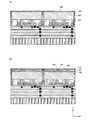
固体撮像装置2の構成の内、画素アレイの構成について、図10および図11を用い説明する。図10は、画素アレイにおける一部領域を抜き出して示す模式平面図であり、図11は、そのB−B’断面、およびB−B’’断面を示す模式断面図であり、半導体基板表面側の読出し回路部の構造を示すB−B’断面と裏面フォトダイオード以降の上部(光入射側)の構造を示すB−B’’断面を組み合わせた模式図であり、構成部位の配置関係については、実際の配置とは異なっている。
[Embodiment 2]
1. Configuration of Pixel Array in Solid-State Imaging Device 2 The configuration of the pixel array in the configuration of the solid-state imaging device 2 will be described with reference to FIGS. 10 and 11. FIG. 10 is a schematic plan view showing a partial region in the pixel array, and FIG. 11 is a schematic cross-sectional view showing the BB ′ cross section and the BB ″ cross section. FIG. 6 is a schematic diagram in which a BB ′ section showing the structure of the readout circuit section and a BB ″ section showing the structure of the upper part (light incident side) after the back surface photodiode are combined. The actual arrangement is different.
図10に示すように、固体撮像装置2においても、フォトダイオード405が形成された領域(画素部)同士の間に画素分離部500が設けられている。そして、各画素部には、接続ダイオード475、蓄積ダイオード406、フローティングディフュージョン407、増幅トランジスタ416、リセットドレイン408が設けられている。また、増幅トランジスタ416のX軸方向の右側には、増幅トランジスタ(Tr)ドレイン415が設けられている。ただし、本実施の形態では、接続ダイオード475に隣接した領域にはオーバーフロードレインは設けられていない。オーバーフロードレイン445は、半導体基板内におけるフォトダイオード405が形成された側に設けられている。
As shown in FIG. 10, also in the solid-state imaging device 2, a
本実施の形態においても、転送ゲート410,411,413,414が設けられ、増幅トランジスタ416の増幅Trゲート412は、ゲート酸化膜の開口417を介して、フローティングディフュージョン407に接続されている。また、リセットドレイン408には、コンタクトプラグ418が接続されており、また、増幅トランジスタ416には、コンタクトプラグ435が接続されている。また、上記同様に、転送ゲート410などには、それぞれコンタクトプラグが接続されている。
Also in this embodiment,
ここで、上記実施の形態1と同様に、蓄積ダイオード406およびフローティングディフュージョン407などは、隣接するフォトダイオード405同士の間の領域(画素分離部500)に配されている。
Here, as in the first embodiment, the
次に、図11に示すように、固体撮像装置2においても、p型の半導体基板401を備え、図のZ軸方向下側の主面にゲート酸化膜404が積層形成され、半導体基板401内における下側主面側の部分には、画素部単位で、STI(Shallow Trench Isolation)402およびp+型のチャネルストッパ403が形成されている。また、ゲート酸化膜404に対しては、Z軸方向下側に、層間絶縁膜420,421,422が順に積層形成され、さらにその下側には、保護膜429が積層され、その下に支持基板460が貼り付けられている。
Next, as shown in FIG. 11, the solid-state imaging device 2 also includes a p-
層間絶縁膜420,421,423には、コンタクトプラグ423,424,425が形成され、互いの境界部分には、配線426,427,428が設けられている。これらについては、材料や形成方法が上記同様である。また、コンタクトプラグ423については、不純物層(リセットドレイン408)との接触抵抗低減のため、チタン(Ti)を、またタングステン(W)との密着を強化するためにTiNが、境界部分に介挿された構成を有する(図示を省略)。
Contact plugs 423, 424, and 425 are formed in the
半導体基板401におけるゲート絶縁膜404側の主面から内方に向けての表層領域には、画素部毎に、接続ダイオード475、蓄積ダイオード406、フローティングディフュージョン407、およびリセットドレイン408が、互いに間隔をあけた状態で設けられている。また、ゲート酸化膜404のZ軸方向下側には、接続ダイオード475と蓄積ダイオード406との間の領域に転送ゲート410のゲート電極が設けられ、蓄積ダイオード406とフローティングディフュージョン407との間の領域に転送ゲート411のゲート電極が設けられ、フローティングディフュージョン407とリセットドレイン408との間の領域に転送ゲート413のゲート電極が設けられている。
In the surface layer region inward from the main surface on the
さらに、フローティングディフュージョン407には、ゲート酸化膜404を挿通する増幅Trゲート412のゲート電極が接続されている。なお、図11では、転送ゲート410,411,413および増幅Trゲート412の各ゲート電極を黒色で示し、不純物拡散層間の対応する各箇所がゲートである。そして、転送ゲート410,411,413および増幅Trゲート412の各ゲート電極は、例えば、Poly−Siにより形成されている。
Further, the floating
なお、接続ダイオード475、蓄積ダイオード406、フローティングディフュージョン407、リセットドレイン408は、n型の不純物拡散層である。そして、図11に示すように、接続ダイオード475に対しては、ゲート酸化膜404との間の領域に、p+型の不純物層であるピニング層430が形成されている。これにより、接続ダイオード475は、埋め込みダイオードになっている。同様に、蓄積ダイオード406に対しては、ゲート酸化膜404との間の領域に、p+型の不純物層であるピニング層431が形成されている。これにより、蓄積ダイオード406についても、埋め込みダイオードになっている。
The
また、本実施の形態においても図示を省略しているが、リセットドレイン408には、ドレイン電圧(VDD)が接続されている。
一方、半導体基板401内のZ軸方向上側の表層部分には、上記実施の形態1と同様に、画素部毎にフォトダイオード405が形成されている。フォトダイオード405は、半導体基板401のZ軸方向上側の主面に沿ってマトリクス状に配されており、各々が対応する接続ダイオード475に接続されている。
Although not shown in the present embodiment, a drain voltage (V DD ) is connected to the
On the other hand, in the surface layer portion on the upper side in the Z-axis direction in the
フォトダイオード405および半導体基板401のZ軸方向上側の面は、ピニング層440により全体が覆われており、その上に反射防止膜441および保護膜443が順に積層形成されている。そして、反射防止膜441の上の保護膜443との境界部分であって、各画素分離部500に対応する領域には、金属配線442が形成されている。金属配線442は、上記実施の形態1と同様に、画素アレイを平面視する場合に、隣接する画素部間を通るようにメッシュ状になっている。
The entire upper surface of the
ここで、画素分離部500においては、隣接するフォトダイオード405同士の間に相当する箇所に、オーバーフロードレイン445が挿設されている。オーバーフロードレイン445は、n型の不純物拡散層からなり、コンタクトプラグ444により金属配線442に接続されている。金属配線442には、正のバイアス電圧が印加可能となっている。金属配線442を介してオーバーフロードレイン445に対して、正のバイアス電圧を印加することにより、フォトダイオード405の信号電荷をリセットすることが可能となる。
Here, in the
保護膜443のZ軸方向上側には、平坦化膜450、カラーフィルタ層451、平坦化膜452、およびマイクロレンズ453が順に積層形成されている。Z軸方向上方より入射した光は、画素部毎にマイクロレンズ453で集光され、光電変換部としてのフォトダイオード405で光電変換される。そして、金属配線442が遮光性を有することから、入射した光が、半導体基板401に形成された各不純物拡散層(蓄積ダイオード406、フローティングディフュージョン407)に入射するのが防止される。
On the upper side of the
なお、図11においては、固体撮像装置2の画素アレイの構成を説明するために、便宜上、蓄積ダイオード406やフローティングディフュージョン407のZ軸方向上方にフォトダイオード405が存在するように図示をしているが、実際には、図10に記載の配置関係を有する。
In FIG. 11, in order to explain the configuration of the pixel array of the solid-state imaging device 2, for the sake of convenience, the
2.固体撮像装置2の駆動
上記構成を有する固体撮像装置2は、グローバル電子シャッター機能を有するのであるが、その駆動について、図12から図14を用い説明する。
2. Driving of Solid-State Imaging Device 2 The solid-state imaging device 2 having the above-described configuration has a global electronic shutter function. The driving thereof will be described with reference to FIGS.
図12(a)は、本発明の実施の形態1に係る固体撮像装置1の内、一つの画素部の等価回路であり、図12(b)は、各ノードのポテンシャルを示すポテンシャル図である。図13は、固体撮像装置1のグローバル電子シャッター動作のタイミングチャートの概略図であり、図14は、固体撮像装置2のグローバル電子シャッター動作時の画素部の動作ポテンシャルの概略図である。
FIG. 12A is an equivalent circuit of one pixel unit in the solid-
図12(a)に示すように、フォトダイオード(PD)405には、オーバーフロードレイン(OFD)445が隣接形成され、また、転送ゲート(GS)410を介して蓄積ダイオード(SD)406が設けられている。なお、図12(a)などにおいても、接続ダイオード475を省略している。
As shown in FIG. 12A, an overflow drain (OFD) 445 is formed adjacent to the photodiode (PD) 405, and a storage diode (SD) 406 is provided via a transfer gate (GS) 410. ing. Note that the
蓄積ダイオード(SD)406に対しては、転送ゲート(TX)411を介して、フローティングディフュージョン(FD)407が設けられ、フローティングディフュージョン(FD)407は、増幅トランジスタ(SF)416のゲート(増幅Trゲート412)に接続され、また、転送ゲート(RS)413を介して、リセットドレイン(RD)408が設けられている。増幅トランジスタ(SF)416のドレイン(SFD)415には、ドレイン電圧(VDD)が接続されている。 The storage diode (SD) 406 is provided with a floating diffusion (FD) 407 via a transfer gate (TX) 411, and the floating diffusion (FD) 407 is connected to the gate (amplification Tr) of the amplification transistor (SF) 416. And a reset drain (RD) 408 is provided via a transfer gate (RS) 413. A drain voltage (V DD ) is connected to the drain (SFD) 415 of the amplification transistor (SF) 416.
次に、図12(b)のポテンシャル図に示すように、上記実施の形態1と同様に、各転送ゲート410,411,413において、ポテンシャルが低くなっており、他の各領域で高くなっている。
Next, as shown in the potential diagram of FIG. 12B, the potential is low in each of the
図13に示すように、転送パルスGSの印加開始タイミングから、次の転送パルスGSの印加開始までが1frameであり、オーバーフロードレイン(OFD)445へのリセットパルスVOFDの印加が終了した直後から、次の転送パルスGSが印加開始されるまでの間が蓄積時間となる。 As shown in FIG. 13, the period from the application start timing of the transfer pulse GS to the start of application of the next transfer pulse GS is 1 frame, and immediately after the application of the reset pulse V OFD to the overflow drain (OFD) 445 is completed, The accumulation time is until the next transfer pulse GS starts to be applied.
具体的に、図13に示すように、1frameの最初に、転送ゲート(GS)410のゲート電極に対して、全ての画素部一括で転送パルスGSを印加する。これにより、フォトダイオード(PD)405に存在する電荷が、一斉に蓄積ダイオード(SD)406に転送される。 Specifically, as shown in FIG. 13, at the beginning of 1 frame, the transfer pulse GS is applied to the gate electrode of the transfer gate (GS) 410 for all the pixel portions at once. As a result, charges existing in the photodiode (PD) 405 are transferred to the storage diode (SD) 406 all at once.
次に、金属電極442を介してオーバーフロードレイン(OFD)445に対して、リセットパルスVOFDを全画素部一斉に印加する。これにより、フォトダイオード(PD)405の信号電荷が、一斉にオーバーフロードレイン(OFD)445に掃き出される(タイミングt11)。オーバーフロードレイン(OFD)445への電荷の掃き出しが行われた後、蓄積時間が開始される。
Next, a reset pulse V OFD is applied to the overflow drain (OFD) 445 through the
次に、n行目に位置する画素部の転送ゲート(RS)413のゲート電極に対しては、リセットパルスRSnが印加され、これにより、n行目のフローティングディフュージョン(FD)407の電荷状態がリセットされる(タイミングt13)。次に、上記のように、転送ゲート(RS)413のゲート電極に対してリセットパルスRSnが印加されたn行目の画素部に対しては、転送ゲート(TX)411のゲート電極に対して、転送パルスTXnが印加される。これにより、蓄積ダイオード(SD)406からフローティングディフュージョン(FD)407へと信号電荷が転送される(タイミングt14)。 Next, with respect to the gate electrode of the transfer gate (RS) 413 of a pixel portion located in the n-th row, the reset pulse RS n is applied, thereby, the charge state of the n-th row of the floating diffusion (FD) 407 Is reset (timing t 13 ). Next, as described above, for the pixel portion in the n-th row where the reset pulse RS n is applied to the gate electrode of the transfer gate (RS) 413, the gate electrode of the transfer gate (TX) 411 is applied. Thus, the transfer pulse TX n is applied. As a result, signal charges are transferred from the storage diode (SD) 406 to the floating diffusion (FD) 407 (timing t 14 ).
同様にして、(n+1)行目の画素部における各転送ゲート(RS,TX)413,411のゲート電極に対して、リセットパルスRSn+1および転送パルスTXn+1がそれぞれ印加される。これにより、(n+1)行目の画素部のフローティングディフュージョン(FD)407の電荷状態がリセットされ、蓄積ダイオード(SD)406からフローティングディフュージョン(FD)407へと信号電荷が転送される。 Similarly, the reset pulse RS n + 1 and the transfer pulse TX n + 1 are respectively applied to the gate electrodes of the transfer gates (RS, TX) 413 and 411 in the pixel portion in the (n + 1) th row. As a result, the charge state of the floating diffusion (FD) 407 in the pixel portion in the (n + 1) th row is reset, and the signal charge is transferred from the storage diode (SD) 406 to the floating diffusion (FD) 407.
なお、上記において、パルスVOFD,GSは、全画素部に対して一斉に印加されるパルスであり、その他のパルスRSn,TXn,RSn+1,TXn+1,・・・は、逐次読み出し動作に従う各行単位に印加されるパルスである。 In the above, the pulses V OFD and GS are pulses applied to all the pixel portions all at once, and the other pulses RS n , TX n , RS n + 1 , TX n + 1 ,. The pulse is applied to each row unit according to.
次に、図14(a)から図14(e)の動作ポテンシャルの概念図を用いて、固体撮像装置2のグローバル電子シャッター動作を説明する。
図14(a)に示すように、タイミングt=t11においては、パルスVOFDがONされ、全画素部のフォトダイオード(PD)405の信号電荷が、一斉にオーバーフロードレイン(OFD)445に排出される。これにより、グローバル電子シャッターの読み出し(蓄積時間の開始)が開始される。
Next, the global electronic shutter operation of the solid-state imaging device 2 will be described using the conceptual diagrams of the operation potentials shown in FIGS. 14 (a) to 14 (e).
As shown in FIG. 14 (a) discharged at the timing t = t 11, the pulse V OFD is turned ON, the signal charge of the photodiode (PD) 405 of all pixel portions, all at once to the overflow drain (OFD) 445 Is done. Thereby, reading of the global electronic shutter (start of accumulation time) is started.
次に、図14(b)に示すようにタイミングt=t12においては、パルスGSはONであり、パルスVOFDはOFFであり、パルスTX(TXn,TXn+1,・・・)もOFFである。そして、パルスGSがONされ、全画素部における転送ゲート(GS)410のゲート電極に一斉に印加されることにより、全画素部におけるフォトダイオード(PD)405の信号電荷が、一斉に蓄積ダイオード(SD)406に転送され、一時蓄積される。そして、これによりグローバル電子シャッターの読み出しが終了(蓄積時間の終了)する。
Next, at a timing t = t 12 as shown in FIG. 14 (b), the pulse GS is ON, the pulse V OFD is OFF, the
また、上述のように、パルスVOFDがOFFになった直後のタイミングt=t11’から、パルスGSがONになった直後のタイミングt=t12’までの蓄積時間が電子シャッター時間となり、任意の時間に設定することができる(図13を参照)。 Further, as described above, the accumulation time from the timing t = t 11 ′ immediately after the pulse V OFD is turned off to the timing t = t 12 ′ immediately after the pulse GS is turned on becomes the electronic shutter time, An arbitrary time can be set (see FIG. 13).
次に、全画素部一斉に信号電荷を蓄積ダイオード406に転送し、蓄積ダイオード406に蓄積されている信号電荷を、逐次読み出しでフローティングディフュージョン407を介して外部に読み出す説明に移る。
Next, a description will be given of a case where all the pixel portions are simultaneously transferred to the
図14(c)に示すように、タイミングt=t13においては、パルスGSおよびパルスVOFDはOFFであり、パルスRSnはONであり、パルスTXnはOFFである。そして、パルスRSnはON状態で、リセットゲート(RS)413のゲート電極に印加されることにより、フローティングディフュージョン(FD)407内の不要電荷はリセットされ、リセット後の電位はドレイン電圧VDDとなる。 As shown in FIG. 14 (c), at time t = t 13, the pulse GS and pulse V OFD is OFF, the pulse RS n is ON, the pulse TX n is OFF. Then, the pulse RS n is in an ON state and is applied to the gate electrode of the reset gate (RS) 413, whereby unnecessary charges in the floating diffusion (FD) 407 are reset, and the potential after the reset is the drain voltage V DD . Become.
次に、蓄積ダイオード(SD)406の信号電荷をフローティングディフュージョン(FD)407に転送する。
図14(d)に示すように、タイミングt=t14においては、パルスGSおよびパルスVOFDはOFFであり、パルスTXnはONであり、パルスRSnはOFFである。そして、パルスTXnがONされ、転送ゲート(TX)411のゲート電極に印加されることにより、パルスTXnが印加される行の蓄積ダイオード(SD)406の電子シャッター後の信号電荷が、フローティングディフュージョン(FD)407に転送される。ここで、転送されてきた信号電荷の量に応じて、フローティングディフュージョン(FD)407の電位がVDDから変化する。この電位変化をソースフォロワーよりなる増幅トランジスタ(SF)416を介して増幅して映像信号として外部に読み出す。
Next, the signal charge of the storage diode (SD) 406 is transferred to the floating diffusion (FD) 407.
As shown in FIG. 14 (d), at time t = t 14, the pulse GS and pulse V OFD is OFF, the pulse TX n is ON, the pulse RS n is OFF. When the pulse TX n is turned on and applied to the gate electrode of the transfer gate (TX) 411, the signal charge after the electronic shutter of the storage diode (SD) 406 in the row to which the pulse TX n is applied is floating. Transfer to diffusion (FD) 407. Here, the potential of the floating diffusion (FD) 407 changes from V DD in accordance with the amount of signal charge transferred. This potential change is amplified via an amplification transistor (SF) 416 made of a source follower and read out as a video signal.
ここで、上記に示すように、蓄積ダイオード(SD)406の信号電荷をフローティングディフュージョン(FD)407に転送するタイミング以外の期間は、パルスRSnはON状態で、転送ゲート(RS)413のゲート電極に印加されることにより、フローティングディフュージョン(FD)407内の不要な電荷はリセットされ続けている。 Here, as shown above, a period other than the timing of transfer of the signal charge accumulation diode (SD) 406 to the floating diffusion (FD) 407, a pulse RS n In the ON state, the gate of the transfer gate (RS) 413 By being applied to the electrodes, unnecessary charges in the floating diffusion (FD) 407 continue to be reset.
次に、(n+1)行目における、蓄積ダイオード(SD)406に蓄積されている信号電荷の逐次読み出しに移る。
図14(e)に示すように、タイミングt=t15においては、パルスGSおよびパルスVOFDはOFFであり、パルスRSn+1はONであり、パルスTXn+1はOFFである。そして、パルスRSn+1がONされ、(n+1)行目の画素部におけるリセットゲート(RS)413のゲート電極に印加されることにより、(n+1)行目の画素部におけるフローティングディフュージョン(FD)内の不要電荷はリセットされ、リセット後の電位はドレイン電圧VDDとなる。
Next, in the (n + 1) th row, the process shifts to sequential readout of signal charges stored in the storage diode (SD) 406.
As shown in FIG. 14 (e), at time t = t 15, the pulse GS and pulse V OFD is OFF, the pulse RS n + 1 is ON, the pulse TX n + 1 is OFF. Then, the pulse RS n + 1 is turned on and applied to the gate electrode of the reset gate (RS) 413 in the pixel portion of the (n + 1) -th row, so that the floating diffusion (FD) in the pixel portion of the (n + 1) -th row is in the floating diffusion (FD). Unnecessary charges are reset, and the reset potential becomes the drain voltage V DD .
これ以降は、図14(c)〜図14(e)の逐次読み出しの駆動のサイクルを全ての行を読み出すまで繰り返し、電子シャッター動作で任意の蓄積時間で撮像した画像の読み出しを終了する。 Thereafter, the sequential readout driving cycle shown in FIGS. 14C to 14E is repeated until all rows are read out, and the readout of the image captured in an arbitrary accumulation time by the electronic shutter operation is completed.
3.効果
本実施の形態に係る固体撮像装置2においても、半導体基板401内の一方の主面側(図11のZ軸方向上側の主面側)にフォトダイオード405を有し、半導体基板401内の他方の主面側(図11のZ軸方向下側の主面側)に蓄積ダイオード406が形成されているため、フォトダイオード405と蓄積ダイオード406とが、占有面積という点において互いにトレードオフの関係にはない。このため、十分な受光部容量と十分な蓄積ダイオード406の容量との両立が可能である。よって、固体撮像装置2においても、グローバル電子シャッター機能を備える固体撮像装置において、画素部のサイズの微細化によっても、十分な光電変換部の面積を確保することができ、高い感度と大きなダイナミックレンジとを実現することができる。
3. Effect Also in the solid-state imaging device 2 according to the present embodiment, the
また、固体撮像装置2では、各画素部におけるオーバーフロードレイン445が、隣接するフォトダイオード405同士の間に設けられている。このため、本実施の形態に係る固体撮像装置2でも、全画素部において、フォトダイオード405の蓄積電荷をオーバーフロードレイン445を介して一括リセットし、その後に、フォトダイオード405で所定時間(シャッター時間)の間で生成された信号電荷を全画素部一斉に読み出して蓄積ダイオード406へと転送し、一時蓄積できる。そして、その後は、上記のように、蓄積ダイオード406からフローティングディフュージョン407に信号電荷が転送され、当該信号電荷に応じてポテンシャル変化が増幅トランジスタ416を介して逐次読み出される。このようにして、本実施の形態に係る固体撮像装置2においても、グローバル電子シャッター機能を備える。
In the solid-state imaging device 2, the
さらに、本実施の形態に係る固体撮像装置2では、オーバーフロードレイン445を、半導体基板401におけるフォトダイオード405が形成されている側の表層部分に設けているので、上記実施の形態1に比べて、オーバーフロードレイン445の形成領域の分だけ蓄積ダイオード406の占有面積を大きくすることができる。
Furthermore, in the solid-state imaging device 2 according to the present embodiment, the
以上のように、本実施の形態に係る固体撮像装置2では、グローバル電子シャッター機能を備え、動きのある撮影においても、高い画質での撮像が可能であり、グローバル電子シャッター機能を備えながら、高い感度を有する。 As described above, the solid-state imaging device 2 according to the present embodiment has a global electronic shutter function, and can capture images with high image quality even in moving shooting. Has sensitivity.
また、本実施の形態に係る固体撮像装置2においても、画素分離部500に遮光性を有する金属配線442が形成されており、蓄積ダイオード406およびフローティングディフュージョン407が、金属配線442の下方に形成されている(図10および図11を参照)。このため、固体撮像装置2においても、隣接するフォトダイオード405同士の間(画素分離部500)を通しての光の入射が防止され、蓄積ダイオード406およびフローティングディフュージョン407での偽信号電荷の発生を防止することができ、これに起因する画質の劣化を防止することができる。よって、本実施の形態に係る固体撮像装置2でも、偽信号電荷の混入が生じることがなく、高い画質を得ることができる。
Also in the solid-state imaging device 2 according to the present embodiment, a
4.固体撮像装置2の製造方法
本実施の形態に係る固体撮像装置2の製造方法について、上記実施の形態1との差異を主に、図15および図16を用い説明する。
4). Manufacturing Method of Solid-State Imaging Device 2 A manufacturing method of the solid-state imaging device 2 according to the present embodiment will be described with reference to FIGS. 15 and 16 mainly with respect to differences from the first embodiment.
図15(a)に示すように、上記実施の形態1と同様の方法により、半導体基板401内におけるZ軸方向上側の部分にフォトダイオード405を形成し、上記同様に、研磨などによりフォトダイオード405を上面に露出させる。また、上記同様に、半導体基板401内の他方の主面側(Z軸方向下側)には、STI402、チャネルストッパ403、接続ダイオード475、蓄積ダイオード406、フローティングディフュージョン407、およびリセットドレイン408が形成され、接続ダイオード475および蓄積ダイオード406は、ピニング層430,431の形成により埋め込みダイオードとなっている。
As shown in FIG. 15A, a
また、半導体基板401の下側主面には、ゲート酸化膜404が形成され、転送ゲート410,411,413および増幅Trゲート412の各ゲート電極が形成されている。さらに、ゲート酸化膜404には、層間絶縁膜420,421,422および保護膜429が積層形成され、コンタクトプラグ423,424,425および配線426,427,428が設けられている。さらに、保護膜429の下側主面には、支持基板460が貼り付けられている。これらの製造方法については、上記の通りである。
Further, a
次に、図15(b)に示すように、半導体基板401におけるZ軸方向上側の主面401fを、バックグラインドやCMP、および化学エッチングで、フォトダイオード405の深さまで研磨した後、フォトダイオード405上に、p+型の不純物となるホウ素(B)をイオン注入する。注入条件は、例えば、5[keV]〜10[keV]、1×10¹¹[cm−2]〜2×10¹²[cm−2]である。この注入により、p+型の不純物拡散層であるピニング層4400が形成される。
Next, as illustrated in FIG. 15B, the
次に、図16(a)に示すように、画素分離部500に相当する領域の半導体基板401(ピニング層4400)に対して、レジスト開口マスクを介して、n型の不純物であるリン(P)や砒素(As)を、例えば、50[keV]〜80[keV]、1×10¹⁴[cm−2]〜2×10¹⁵[cm−2]でイオン注入する。これにより、半導体基板401内の隣接するフォトダイオード405同士の間に、オーバーフロードレイン445を形成することができる。ここで、オーバーフロードレイン445は、ピニング層440も挿通した状態で形成される。
Next, as shown in FIG. 16A, phosphorus (P), which is an n-type impurity, is applied to the semiconductor substrate 401 (pinning layer 4400) in the region corresponding to the
次に、図16(b)に示すように、ピニング層440およびオーバーフロードレイン445上に、低温のCVD膜である反射防止膜441を、例えば、数10[nm]〜数100[nm]の膜厚で形成する。次に、反射防止膜441上のオーバーフロードレイン445に相当する箇所に対して、所定のパターンのレジスト開口マスクを形成し、ドライエッチング技術で該当箇所を開口し、n型のオーバーフロードレイン445上にコンタクト孔を形成する。そして、スパッタリングやCVDで、例えば、膜厚が100[nm]〜300[nm]のアルミニウム(Al)やタングステン(W)、モリブデン(Mo)、TiN等からなる金属膜を堆積し、その後に、フォトリソグラフィ技術とエッチング技術とにより、当該金属膜をエッチングし、反射防止膜441の画素分離部500に相当する領域に、オーバーフロードレイン445と接続されたコンタクトプラグ444およびメッシュ状の金属配線442を形成する。
Next, as shown in FIG. 16B, an
次に、CVD酸化膜やプラズマ酸化膜よりなる保護膜443を形成する。
この後の工程については、図示を省略しているが、上記実施の形態1と同様に、保護膜443上に、透明の有機膜よりなる平坦化膜450、顔料を含んだ有機膜よりなるカラーフィルタ層451、透明の有機膜よりなる平坦化膜452、および透明の有機膜よりなるマイクロレンズ453を順に形成して、固体撮像装置2は完成する(図11を参照)。
Next, a
Although the illustration of the subsequent steps is omitted, as in the first embodiment, a flattening
[実施の形態3]
1.固体撮像装置3における画素アレイの構成
固体撮像装置3の構成の内、画素アレイの構成について、図17を用い説明する。図17では、画素アレイにおける一部の画素部600を抜き出して模式的に図示している。
[Embodiment 3]
1. Configuration of Pixel Array in Solid-State Imaging Device 3 Among the configurations of the solid-state imaging device 3, the configuration of the pixel array will be described with reference to FIG. In FIG. 17, a part of the
図17に示すように、固体撮像装置3の構成は、基本的な部分において、上記実施の形態2と同様である。即ち、図17に示すように、p型の半導体基板601に対し、Z軸方向下側の主面にゲート酸化膜604が積層形成され、半導体基板601内における下側主面側の部分には、画素部単位で、STI(Shallow Trench Isolation)602およびp+型のチャネルストッパ603が形成されている。また、ゲート酸化膜604に対しては、Z軸方向下側に、層間絶縁膜620,621,622が順に積層形成され、さらにその下側には、保護膜629が積層され、その下に支持基板660が貼り付けられている。
As shown in FIG. 17, the configuration of the solid-state imaging device 3 is the same as that of the second embodiment in the basic part. That is, as shown in FIG. 17, a
層間絶縁膜620,621,623には、コンタクトプラグ623,624,625が形成され、互いの境界部分には、配線626,627,628が設けられている。これらについては、材料や形成方法が上記同様である。また、コンタクトプラグ623については、不純物層(リセットドレイン608)との接触抵抗低減のため、チタン(Ti)を、またタングステン(W)との密着を強化するためにTiNが、境界部分に介挿された構成を有する(図示を省略)。
Contact plugs 623, 624, and 625 are formed in the
半導体基板601におけるゲート絶縁膜604側の主面から内方に向けての表層領域には、画素部毎に、接続ダイオード675、蓄積ダイオード606、フローティングディフュージョン607、およびリセットドレイン608が設けられ、また、転送ゲート610,611,613および増幅Trゲート612の各ゲート電極が設けられている。各ゲート電極は、例えば、Poly−Siにより形成されている。
A
また、接続ダイオード675および蓄積ダイオード606は、ピニング層630,631の形成により埋め込みダイオードになっている。また、本実施の形態においても図示を省略しているが、リセットドレイン608には、ドレイン電圧(VDD)が接続されている。
The
一方、半導体基板601内のZ軸方向上側の表層部分には、上記実施の形態1と同様に、画素部毎にフォトダイオード605が形成され、各々が対応する接続ダイオード675に接続されている。フォトダイオード605および半導体基板601のZ軸方向上側には、ピニング層640、反射防止膜641および保護膜643が順に積層形成されており、さらに、その上に、平坦化膜650、カラーフィルタ層651、平坦化膜452、およびマイクロレンズ653が順に積層形成されている。
On the other hand, in the surface layer portion on the upper side in the Z-axis direction in the
本実施の形態では、上記実施の形態2と同様に、反射防止膜641の上の保護膜643との境界部分であって、各画素分離部700に対応する領域には、金属配線642が形成されている。金属配線642は、上記実施の形態1と同様に、画素アレイを平面視する場合に、隣接する画素部間を通るようにメッシュ状になっている。
In the present embodiment, similarly to the second embodiment, a
ここで、画素分離部700においては、隣接するフォトダイオード605同士の間に相当する箇所に、オーバーフロードレイン645が挿設されており、コンタクトプラグ644により金属配線642に接続されている。金属配線642には、正のバイアス電圧が印加可能となっている点も上記実施の形態2と同様である。本実施の形態に係る固体撮像装置3が上記実施の形態2に係る固体撮像装置2と異なるのは、各オーバーフロードレイン645に対応して、n−型の不純物拡散層であるオーバーフロードレイン(OFD)バリア層646が形成されている点にある。
Here, in the
本実施の形態に係る固体撮像装置3では、外部から金属配線642を介してオーバーフロードレイン645に対して、正のバイアス電圧を印加することにより、オーバーフロードレイン645の電位をコントロールし、OFDバリア層646を介して、フォトダイオード605の電荷をリセットすることが可能である。
In the solid-state imaging device 3 according to the present embodiment, the potential of the
2.効果
本実施の形態に係る固体撮像装置3も、上記実施の形態2に係る固体撮像装置2と同じ効果を奏する。これに加えて、本実施の形態に係る固体撮像装置3では、OFDバリア層646の形成により、より確実なフォトダイオード605の電荷のリセットが可能となり、グローバル電子シャッター機能を有し、且つ、さらに高い画質性能を有する。
2. Effects The solid-state imaging device 3 according to the present embodiment also has the same effects as the solid-state imaging device 2 according to the second embodiment. In addition to this, in the solid-state imaging device 3 according to the present embodiment, the formation of the
3.固体撮像装置3の製造方法
本実施の形態に係る固体撮像装置3の製造方法は、概略、上記実施の形態2と同様であるが、その差異のみを説明する。具体的に、本実施の形態に係る固体撮像装置3の製造方法が上記実施の形態2に係る固体撮像装置2の製造方法と異なるところ、OFDバリア層646を形成するところである。
3. Manufacturing Method of Solid-State Imaging Device 3 The manufacturing method of the solid-state imaging device 3 according to the present embodiment is generally the same as that of the second embodiment, but only the difference will be described. Specifically, the manufacturing method of the solid-state imaging device 3 according to the present embodiment is different from the manufacturing method of the solid-state imaging device 2 according to the second embodiment, and the
具体的には、画素分離部700に相当する領域の半導体基板601に、レジスト開口マスクを介して、n型の不純物であるリン(P)や砒素(As)を、例えば、50[keV]〜80[keV]、1×10¹⁴[cm−2]〜2×10¹⁵[cm−2]で、イオン注入して、オーバーフロードレイン645を形成する。そして、オーバーフロードレイン645の注入条件より、不純物濃度が小さくし、注入深さが深い注入条件により、例えば、リン(P)や砒素(As)を、60[keV]〜90[keV]、1×10¹³[cm−2]〜2×10¹⁴[cm−2]で、イオン注入して、OFDバリア層646を形成することができる。
Specifically, phosphorus (P) or arsenic (As), which are n-type impurities, are applied to the
なお、OFDバリア層646は、特段の処理を施すことなく形成される場合もあるが、それでも同様の機能をえることができる。上記工程以外は、実施の形態2と同じなので、説明を省略する。
Note that the
[その他の事項]
上記実施の形態1,2,3に係る固体撮像装置1,2,3では、画素部100,600,・・毎にオーバーフロードレイン109,445,645を設ける構成としたが、二つの画素部、あるいはそれ以上の数の画素部で、一つのオーバーフロードレインを共有する構成とすることもできる。同様に、リセットドレイン108,408,608についても、一つの画素部あるいはそれ以上の数の画素部で、一つのリセットドレインを共有する構成とすることもできる。
[Other matters]
In the solid-
また、上記実施の形態1,2,3に係る固体撮像装置では、画素アレイ10,・・において、複数の画素部100,600,・・が行列(マトリクス)状に配されている構成としたが、画素部の配列構成はこれに限定されるものではなく、例えば、ハニカム状に配列されていてもよい。
In the solid-state imaging device according to the first, second, and third embodiments, a plurality of
また、上記実施の形態1,2,3に係る固体撮像装置1,2,3では、マイクロレンズ153,453,653が最もトップ側に各一つ設けられている構成としたが、凸レンズと凹レンズとの組み合わせ、あるいは、凸レンズと凸レンズの組み合わせ、さらには、凹レンズと凹レンズの組み合わせとすることも可能である。
In the solid-
本発明は、グローバル電子シャッター機能を有し、動きのある被写体に対しても高い画質での撮像が可能であり、且つ、高い感度での撮像が可能な固体撮像装置を実現するのに有用である。 The present invention is useful for realizing a solid-state imaging device having a global electronic shutter function, capable of capturing a moving subject with high image quality, and capable of capturing with high sensitivity. is there.
1,2,3.固体撮像装置
10.画素アレイ
21.パルス発生回路
22.水平シフトレジスタ
23.垂直シフトレジスタ
100,700.画素部
101,401,601,1010.半導体基板
102,402,602.STI
103,403,603.チャネルストッパ
104,404,604,1040.ゲート酸化膜
105,405,605.フォトダイオード
106,406,606.蓄積ダイオード
107,407,607.フローティングディフュージョン
108,408,608.リセットドレイン
109,445,645.オーバーフロードレイン
110,111,113,114,410,411,413,610,611,613.転送ゲート
112,412,612.増幅Trゲート
115,415.増幅Trドレイン
116,416.増幅トランジスタ
117,417.ゲート酸化膜の開口
118,119,123,124,125,135,136,418,423,424,425,435,444,623,624,625,644.コンタクトプラグ
120,121,122,420,421,422,620,621,622.層間絶縁膜
126,127,128,426,427,626,627,628.配線
130,131,140,430,431,440,4400,630,631,640.ピニング層
142,442,642.金属配線
129,143,429,443,629,643.保護膜
141,441,641.反射防止膜
150,152,450,452,650,652.平坦化膜
151,451,651.カラーフィルタ層
153,453,653.マイクロレンズ
160,460,660.支持基板
175,475,675.接続ダイオード
300,500,700.画素分離部
646.OFDバリア層
1,2,3. Solid-
103, 403, 603.
Claims (6)
前記半導体基板内における第1の主面側に、当該第1の主面に沿う状態で、且つ、互いの間に間隔をあけた状態で二次元形成された複数の光電変換部と、
前記半導体基板内における前記第1の主面とは反対側の第2の主面側に、前記複数の光電変換部の各々に対応して設けられ、且つ、対応する前記光電変換部に接続された接続ダイオードと、
前記半導体基板内における前記第2の主面側に、前記接続ダイオードの各々に対応し、且つ、対応する前記接続ダイオードと第1ゲートを介して設けられた蓄積ダイオードと、
前記半導体基板内における前記第2の主面側に、前記接続ダイオードの各々に対応し、且つ、対応する前記接続ダイオードと第2ゲートを介して設けられたオーバーフロードレインと、
を有する
ことを特徴とする固体撮像装置。 A semiconductor substrate;
A plurality of photoelectric conversion units that are two-dimensionally formed on the first main surface side in the semiconductor substrate in a state along the first main surface and with a space between each other;
A second main surface side opposite to the first main surface in the semiconductor substrate is provided corresponding to each of the plurality of photoelectric conversion units and connected to the corresponding photoelectric conversion unit. Connected diodes,
A storage diode provided on the second main surface side in the semiconductor substrate, corresponding to each of the connection diodes, and provided via the corresponding connection diode and the first gate;
An overflow drain corresponding to each of the connection diodes on the second main surface side in the semiconductor substrate and provided via the corresponding connection diode and the second gate;
A solid-state imaging device characterized by comprising:
前記半導体基板内における第1の主面側に、当該第1の主面に沿う状態で、且つ、互いの間に間隔をあけた状態で二次元形成された複数の光電変換部と、
前記半導体基板内における前記第1の主面とは反対側の第2の主面側に、前記複数の光電変換部の各々に対応して設けられ、且つ、対応する前記光電変換部に接続された接続ダイオードと、
前記半導体基板内における前記第2の主面側に、前記接続ダイオードの各々に対応し、且つ、対応する前記接続ダイオードと第1ゲートを介して設けられた蓄積ダイオードと、
前記半導体基板内における前記第1の主面側に、隣接する前記光電変換部同士の間に設けられたオーバーフロードレインと、
を有する
ことを特徴とする固体撮像装置。 A semiconductor substrate;
A plurality of photoelectric conversion units that are two-dimensionally formed on the first main surface side in the semiconductor substrate in a state along the first main surface and with a space between each other;
A second main surface side opposite to the first main surface in the semiconductor substrate is provided corresponding to each of the plurality of photoelectric conversion units and connected to the corresponding photoelectric conversion unit. Connected diodes,
A storage diode provided on the second main surface side in the semiconductor substrate, corresponding to each of the connection diodes, and provided via the corresponding connection diode and the first gate;
An overflow drain provided between the adjacent photoelectric conversion units on the first main surface side in the semiconductor substrate;
A solid-state imaging device characterized by comprising:
前記半導体基板内における前記第2の主面側に、前記蓄積ダイオードの各々に対応し、且つ、対応する前記蓄積ダイオードと第3ゲートを介して設けられたフローティングディフュージョンを有する
ことを特徴とする請求項1または請求項2に記載の固体撮像装置。 further,
The floating diffusion provided on the second main surface side in the semiconductor substrate, corresponding to each of the storage diodes, and provided via the corresponding storage diode and a third gate. Item 3. The solid-state imaging device according to Item 1 or 2.
前記フローティングディフュージョンは、前記半導体基板における前記第1の主面側上方の少なくとも一部が、前記金属膜で覆われている
ことを特徴とする請求項3に記載の固体撮像装置。 Above the second main surface of the semiconductor substrate, a light-shielding metal film is formed in a portion corresponding to the space between the adjacent photoelectric conversion portions,
4. The solid-state imaging device according to claim 3, wherein at least a part of the floating diffusion above the first main surface side of the semiconductor substrate is covered with the metal film.
前記蓄積ダイオードは、前記半導体基板における前記第1の主面側上方の少なくとも一部が、前記金属膜で覆われている
ことを特徴とする請求項1から請求項3の何れかに記載の固体撮像装置。 Above the second main surface of the semiconductor substrate, a light-shielding metal film is formed in a portion corresponding to the space between the adjacent photoelectric conversion portions,
4. The solid according to claim 1, wherein at least a part of the storage diode above the first main surface side of the semiconductor substrate is covered with the metal film. 5. Imaging device.
前記オーバーフロードレインは、前記金属膜に接続されており、当該金属膜を介して前記バイアス電圧印加部からのバイアス電圧の印加を受ける
ことを特徴とする請求項2に記載の固体撮像装置。 Above the second main surface of the semiconductor substrate, a light-shielding metal film is formed in a portion corresponding to the space between the adjacent photoelectric conversion portions,
The solid-state imaging device according to claim 2, wherein the overflow drain is connected to the metal film and receives a bias voltage from the bias voltage application unit via the metal film.
Priority Applications (1)
| Application Number | Priority Date | Filing Date | Title |
|---|---|---|---|
| JP2011066479A JP2012204524A (en) | 2011-03-24 | 2011-03-24 | Solid state image pickup device |
Applications Claiming Priority (1)
| Application Number | Priority Date | Filing Date | Title |
|---|---|---|---|
| JP2011066479A JP2012204524A (en) | 2011-03-24 | 2011-03-24 | Solid state image pickup device |
Publications (1)
| Publication Number | Publication Date |
|---|---|
| JP2012204524A true JP2012204524A (en) | 2012-10-22 |
Family
ID=47185203
Family Applications (1)
| Application Number | Title | Priority Date | Filing Date |
|---|---|---|---|
| JP2011066479A Withdrawn JP2012204524A (en) | 2011-03-24 | 2011-03-24 | Solid state image pickup device |
Country Status (1)
| Country | Link |
|---|---|
| JP (1) | JP2012204524A (en) |
Cited By (6)
| Publication number | Priority date | Publication date | Assignee | Title |
|---|---|---|---|---|
| JP2015188049A (en) * | 2014-03-14 | 2015-10-29 | キヤノン株式会社 | Solid state image pickup device and image pickup system |
| KR20160088471A (en) * | 2015-01-15 | 2016-07-26 | 삼성전자주식회사 | Image sensors |
| US9887217B2 (en) | 2014-10-16 | 2018-02-06 | Samsung Electronics Co., Ltd. | Pixels of image sensors, image sensors including the pixels, and image processing systems including the image sensors |
| US9947703B2 (en) | 2014-02-18 | 2018-04-17 | Sony Semiconductor Solutions Corporation | Solid-state imaging device, method of manufacturing the same, and electronic apparatus |
| JP2018160667A (en) * | 2017-03-22 | 2018-10-11 | パナソニックIpマネジメント株式会社 | Solid-state image pickup device |
| CN110164904A (en) * | 2018-02-12 | 2019-08-23 | 三星电子株式会社 | Imaging sensor and its manufacturing method |
-
2011
- 2011-03-24 JP JP2011066479A patent/JP2012204524A/en not_active Withdrawn
Cited By (9)
| Publication number | Priority date | Publication date | Assignee | Title |
|---|---|---|---|---|
| US9947703B2 (en) | 2014-02-18 | 2018-04-17 | Sony Semiconductor Solutions Corporation | Solid-state imaging device, method of manufacturing the same, and electronic apparatus |
| JP2015188049A (en) * | 2014-03-14 | 2015-10-29 | キヤノン株式会社 | Solid state image pickup device and image pickup system |
| US9887217B2 (en) | 2014-10-16 | 2018-02-06 | Samsung Electronics Co., Ltd. | Pixels of image sensors, image sensors including the pixels, and image processing systems including the image sensors |
| KR20160088471A (en) * | 2015-01-15 | 2016-07-26 | 삼성전자주식회사 | Image sensors |
| KR102363433B1 (en) | 2015-01-15 | 2022-02-16 | 삼성전자주식회사 | Image sensors |
| JP2018160667A (en) * | 2017-03-22 | 2018-10-11 | パナソニックIpマネジメント株式会社 | Solid-state image pickup device |
| JP7178605B2 (en) | 2017-03-22 | 2022-11-28 | パナソニックIpマネジメント株式会社 | Solid-state imaging device |
| CN110164904A (en) * | 2018-02-12 | 2019-08-23 | 三星电子株式会社 | Imaging sensor and its manufacturing method |
| CN110164904B (en) * | 2018-02-12 | 2023-12-29 | 三星电子株式会社 | Image sensor and method of manufacturing the same |
Similar Documents
| Publication | Publication Date | Title |
|---|---|---|
| JP5533046B2 (en) | Solid-state imaging device, method for manufacturing solid-state imaging device, driving method for solid-state imaging device, and electronic apparatus | |
| JP5564847B2 (en) | SOLID-STATE IMAGING DEVICE, ITS MANUFACTURING METHOD, AND ELECTRONIC DEVICE | |
| US8669135B2 (en) | System and method for fabricating a 3D image sensor structure | |
| US8471315B1 (en) | CMOS image sensor having global shutter pixels built using a buried channel transfer gate with a surface channel dark current drain | |
| JP4752926B2 (en) | Solid-state imaging device, manufacturing method of solid-state imaging device, driving method of solid-state imaging device, electronic apparatus | |
| JP6186205B2 (en) | Imaging device and imaging apparatus | |
| WO2012117670A1 (en) | Solid-state imaging device | |
| US8928792B1 (en) | CMOS image sensor with global shutter, rolling shutter, and a variable conversion gain, having pixels employing several BCMD transistors coupled to a single photodiode and dual gate BCMD transistors for charge storage and sensing | |
| TWI501389B (en) | Image sensors having frontside and backside photodetectors | |
| US20100327388A1 (en) | Back-illuminated image sensors having both frontside and a backside photodetectors | |
| JP2013012556A (en) | Solid-state image pickup device, manufacturing method of the same and electronic apparatus | |
| WO2018173788A1 (en) | Imaging element and electronic device | |
| JP2011204797A (en) | Solid-state imaging apparatus, method of manufacturing the same, and electronic equipment | |
| JP2012199489A (en) | Solid state image pickup device, solid state image pickup device manufacturing method and electronic apparatus | |
| US8427568B2 (en) | Solid-state image pickup device, method for manufacturing the same, and electronic apparatus | |
| WO2013094430A1 (en) | Solid-state image pickup device, manufacturing method for solid-state image pickup device, and electronic equipment | |
| US20210217787A1 (en) | Imaging device and electronic device | |
| WO2018100998A1 (en) | Solid-state imaging element, method for manufacturing solid-state imaging element, and imaging device | |
| WO2012120807A1 (en) | Solid-state imaging device | |
| JP2013012551A (en) | Solid-state imaging apparatus, method of manufacturing solid-state imaging apparatus, and electronic apparatus | |
| TWI617014B (en) | Solid-state imaging device, manufacturing method, and electronic device | |
| KR20140125762A (en) | Solid-state image pickup apparatus, method for manufacturing solid-state image pickup apparatus, and electronic apparatus | |
| JP2012204524A (en) | Solid state image pickup device | |
| TW201222802A (en) | Solid-state imaging device, manufacturing method of solid-state imaging device, and electronic apparatus | |
| WO2012001836A1 (en) | Solid-state imaging element |
Legal Events
| Date | Code | Title | Description |
|---|---|---|---|
| A300 | Withdrawal of application because of no request for examination |
Free format text: JAPANESE INTERMEDIATE CODE: A300 Effective date: 20140603 |