JP2012203929A - Semiconductor memory - Google Patents
Semiconductor memory Download PDFInfo
- Publication number
- JP2012203929A JP2012203929A JP2011065031A JP2011065031A JP2012203929A JP 2012203929 A JP2012203929 A JP 2012203929A JP 2011065031 A JP2011065031 A JP 2011065031A JP 2011065031 A JP2011065031 A JP 2011065031A JP 2012203929 A JP2012203929 A JP 2012203929A
- Authority
- JP
- Japan
- Prior art keywords
- bit line
- transistor
- memory cell
- control circuit
- current path
- Prior art date
- Legal status (The legal status is an assumption and is not a legal conclusion. Google has not performed a legal analysis and makes no representation as to the accuracy of the status listed.)
- Withdrawn
Links
Images


Classifications
-
- G—PHYSICS
- G11—INFORMATION STORAGE
- G11C—STATIC STORES
- G11C16/00—Erasable programmable read-only memories
- G11C16/02—Erasable programmable read-only memories electrically programmable
- G11C16/06—Auxiliary circuits, e.g. for writing into memory
- G11C16/26—Sensing or reading circuits; Data output circuits
Abstract
Description
本発明の実施形態は、半導体記憶装置に関する。 Embodiments described herein relate generally to a semiconductor memory device.
従来、NAND型フラッシュ・メモリの読み出し速度は、主にビット線のリカバリ時間に律束されている。このリカバリ時間とは、ビット線電位がディスターブを受けた時に、該ビット線の電位を元の電位に戻す時間である。そして、このリカバリ時間は、該ビット線と、隣接/第2隣接ビット線との容量結合や、該ビット線の充電能力に依存して決まる。微細化に伴い、セル電流が減少し、該ビット線と隣接/第2隣接ビット線との相互干渉が増加しているため、読み出し特性は更に悪化していく。 Conventionally, the read speed of the NAND flash memory is mainly limited by the recovery time of the bit line. The recovery time is a time for returning the bit line potential to the original potential when the bit line potential is disturbed. The recovery time is determined depending on the capacitive coupling between the bit line and the adjacent / second adjacent bit line and the charging capability of the bit line. Along with miniaturization, the cell current decreases, and the mutual interference between the bit line and the adjacent / second adjacent bit line increases, so that the read characteristics are further deteriorated.
また、NAND型フラッシュ・メモリの内部動作として一般に行われる書き込み、または消去動作時のメモリ・セルの閾値検査(以下ベリファイ)も読み出し動作である。このため、読み出し特性だけではなく、書き込み、または消去特性についても同様に劣化する傾向にある。 In addition, a memory cell threshold test (hereinafter referred to as verify) during a write or erase operation generally performed as an internal operation of the NAND flash memory is also a read operation. For this reason, not only the reading characteristics but also the writing or erasing characteristics tend to deteriorate similarly.
ビット線のリカバリ時間を短縮し、高速な動作を実現することが可能な半導体記憶装置を提供する。 Provided is a semiconductor memory device capable of reducing bit line recovery time and realizing high-speed operation.
実施形態の半導体記憶装置は、電気的に書き換えが可能なメモリ・セルと、前記メモリ・セルのゲートに接続されるワード線と、前記メモリ・セルの電流経路の一端に接続されるビット線と、電流経路の一端が、前記ビット線と接続される第1のクランプ・トランジスタと、互いに電気的に接続される第2のクランプ・トランジスタ、及びスイッチ回路を備え、前記ビット線及び前記第1のクランプ・トランジスタの電流経路の一端と接続される電圧制御回路と、前記第1のクランプ・トランジスタの電流経路の他端と、前記電圧制御回路と接続されるセンス・アンプと、前記センス・アンプと電気的に接続され、前記メモリ・セルの読み出しを行う前に第1のデータを保持し、前記ビット線に所定電流以上の電流が流れた場合は第2のデータを保持するデータ・ラッチ部と、前記データ・ラッチ部に第2のデータが保持された場合、前記ビット線の電位をリセット電位に落とすプル・ダウン回路と、前記メモリ・セルの読み出しを行う際に、前記ビット線に第1のクランプ・トランジスタのゲート及び第2のクランプ・トランジスタのゲートに、所定の電位を与える充電制御回路と、を備え、前記ワード線方向で隣接する他のデータ・ラッチ部に保持されているデータに依存し、前記スイッチ回路がオン、またはオフすることにより、前記電圧制御回路を介して、前記ビット線と前記センス・アンプとの間の接続が制御される。 The semiconductor memory device of the embodiment includes an electrically rewritable memory cell, a word line connected to the gate of the memory cell, and a bit line connected to one end of a current path of the memory cell. , One end of the current path includes a first clamp transistor connected to the bit line, a second clamp transistor electrically connected to each other, and a switch circuit, the bit line and the first A voltage control circuit connected to one end of the current path of the clamp transistor, the other end of the current path of the first clamp transistor, a sense amplifier connected to the voltage control circuit, and the sense amplifier; It is electrically connected and holds the first data before reading the memory cell. If a current greater than a predetermined current flows through the bit line, the second data is stored. A data latch unit for holding data, a pull-down circuit for dropping the potential of the bit line to a reset potential when second data is held in the data latch unit, and when reading the memory cell And a charge control circuit for applying a predetermined potential to the gate of the first clamp transistor and the gate of the second clamp transistor on the bit line, and another data latch adjacent in the word line direction. Depending on the data held in the unit, the switch circuit is turned on or off, whereby the connection between the bit line and the sense amplifier is controlled via the voltage control circuit.
以下、実施形態の詳細を図面を参照して説明する。この説明に際し、全図にわたり、共通する部分には共通する参照符号を付す。 Hereinafter, the details of the embodiment will be described with reference to the drawings. In the description, common parts are denoted by common reference symbols throughout the drawings.
(第1の実施形態)
<NAND型フラッシュ・メモリの全体構成>
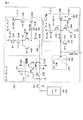
図1、及び図2を用いて、第1の実施形態に係るNAND型フラッシュ・メモリの構成を概略的に説明する。図1は、第1の実施形態に係るNAND型フラッシュ・メモリ100の基本的な構成を模式的に示すブロック図である。また、図2は、図1に示すメモリ・セル・アレイ1、ビット線制御回路2、およびロウ・デコーダ6を含む、第1の実施形態に係るNAND型フラッシュ・メモリ100の基本的な構成を模式的に示す回路図である。
(First embodiment)
<Overall configuration of NAND flash memory>
The configuration of the NAND flash memory according to the first embodiment will be schematically described with reference to FIGS. 1 and 2. FIG. 1 is a block diagram schematically showing a basic configuration of a
図1に示すように、NAND型フラッシュ・メモリ100は、メモリ・セル・アレイ1と、ビット線制御回路2と、カラム・デコーダ3と、データ入出力バッファ4と、データ入出力端子5と、ロウ・デコーダ6と、制御回路7と、制御信号入力端子8と、ソース線制御回路9と、ウェル制御回路10と、を備える。
As shown in FIG. 1, the
メモリ・セル・アレイ1は、複数のビット線BLと、複数のワード線WLと、ソース線SRCとを含む。このメモリ・セル・アレイ1は、電気的に書き換えが可能なメモリ・セルMCがマトリクス状に配置された複数のブロックBLKで構成されている。メモリ・セルMCは、例えば、制御ゲート電極及び浮遊ゲート電極を含む積層構造からなり、浮遊ゲート電極に注入された電荷量により定まるトランジスタの閾値の変化によって二値、あるいは多値データを記憶する。また、メモリ・セルMCは、窒化膜に電子をトラップするMONOS(Metal - Oxide - Nitride - Oxide - Silicon)構造を有するものであっても良い。
このメモリ・セル・アレイ1には、ビット線選択NMOSトランジスタ20を介してビット線BLの電圧を制御するためのビット線制御回路2と、ワード線WLの電圧を制御するためのロウ・デコーダ6とが接続されている。データの消去動作時には、何れかのブロックBLKがロウ・デコーダ6により選択され、残りのブロックBLKが非選択とされる。
The
ビット線制御回路2は、後述するクランプ用のNMOSトランジスタ(クランプ・トランジスタとも呼ぶ)を制御する充電制御回路2−1、及びセンス・モジュール2−2を含む。センス・モジュール2−2は、メモリ・セル・アレイ1内のビット線BLの電圧をセンス増幅するセンス・アンプ(S/A)2−3と、書き込みを行うためのデータをラッチするためのデータ・ラッチ回路との両方の役割を持つデータ記憶回路(データ・ラッチ部)2−5と、ビット線の電位を接地電位(GND)に下げるプル・ダウン回路2−6と、隣接するビット線の電位に応じて対応するビット線の充電を加速させる加速器(電圧制御回路)2−4と、を備える。
The bit
このビット線制御回路2は、ビット線BLを介してメモリ・セル・アレイ1中のメモリ・セルMCのデータを読み出したり、ビット線BLを介して該メモリ・セルMCの状態を検出したり、ビット線BLを介して該メモリ・セルMCに書き込み制御電圧を印加して該メモリ・セルMCに書き込みを行う。
The bit
また、ビット線制御回路2には、カラム・デコーダ3、データ入出力バッファ4が接続されている。ビット線制御回路2内の該データ記憶回路は、カラム・デコーダ3により選択され、このデータ記憶回路に読み出されたメモリ・セルMCのデータは、データ入出力バッファ4を介してデータ入出力端子5から外部へ出力される。
Further, a
また、外部からデータ入出力端子5に入力された書き込みデータは、データ入出力バッファ4を介して、カラム・デコーダ3によって選択された該データ記憶回路に記憶される。データ入出力端子5からは、書き込みデータの他に、書き込み、読み出し、消去、およびステータス・リード等の各種コマンド、アドレスも入力される。
Write data input from the outside to the data input /
ロウ・デコーダ6は、メモリ・セル・アレイ1に接続されている。このロウ・デコーダ6は、メモリ・セル・アレイ1のワード線WL及び選択ゲート線VSGS、VSGDに、読み出し動作、書き込み動作、或いは消去動作において必要な電圧を印加する。また、ロウ・デコーダ6は、ワード線WL及び選択ゲート線VSGS、VSGDに選択的に電圧を印加するために、後述する複数の制御線に接続されたドライバ制御回路6−1を含む。
The row decoder 6 is connected to the
ソース線制御回路9は、メモリ・セル・アレイ1に接続されている。ソース線制御回路9は、ソース線SRCの電圧を制御する。
The source
ウェル制御回路10は、メモリ・セル・アレイ1に接続されている。このウェル制御回路10は、メモリ・セルMCが形成される半導体基板(ウェル)の電圧を制御するようになっている。
The
制御回路7は、メモリ・セル・アレイ1、ビット線制御回路2、カラム・デコーダ3、データ入出力バッファ4、ロウ・デコーダ6、ソース線制御回路9、および、ウェル制御回路10を制御する。制御回路7には、電源電圧を昇圧する昇圧回路(図示せず)が含まれているものとする。制御回路7は、該昇圧回路により電源電圧を必要に応じて昇圧し、ビット線制御回路2、カラム・デコーダ3、データ入出力バッファ4、ロウ・デコーダ6、ソース線制御回路9、および、ウェル制御回路10に供給する。
The
制御回路7は、外部から制御信号入力端子8を介して入力される制御信号(コマンド・ラッチ・イネーブル信号CLE、アドレス・ラッチ・イネーブル信号ALE、レディ/ビジー信号RY/BY等)およびデータ入出力端子5からデータ入出力バッファ4を介して入力されるコマンドに応じて制御動作する。すなわち、制御回路7は、該制御信号およびコマンドに応じて、データのプログラム、ベリファイ、読み出し、消去時に、所望の電圧を発生し、メモリ・セル・アレイ1の各部に供給する。
The
ここで、図2に示すように、メモリ・セル・アレイ1は、直列接続された複数のメモリ・セルMCからなるNANDストリングが平行に配置されて構成されるブロックBLK0、BLK1、…BLKnを有する。NANDストリングは直列接続されたn(例えば64)個のメモリ・セルMCから構成され、NANDストリングの一端にはドレイン側選択MOSトランジスタSGDが、他端にはソース側選択MOSトランジスタSGSが接続されている。また、ソース側選択MOSトランジスタSGSは、ソース線SRCに接続されている。
Here, as shown in FIG. 2, the
各行に配置されたメモリ・セルMCの制御ゲート電極は、それぞれ、ワード線WL0〜WLnに接続されている。なお、図2では、簡単のため、ワード線WL0、WL1、WLn−1、WLnのみを表記しており、その間に配置されるワード線は省略している。以下、複数のワード線を特に区別する必要がない場合は、単にワード線WLと表記する場合がある。ドレイン側選択MOSトランジスタSGDのゲートは、ドレイン側選択ゲート線VSGDに接続されている。ソース側選択MOSトランジスタSGSのゲートは、ソース側選択ゲート線VSGSに接続されている。 The control gate electrodes of the memory cells MC arranged in each row are connected to the word lines WL0 to WLn, respectively. In FIG. 2, for simplicity, only the word lines WL0, WL1, WLn-1, and WLn are shown, and the word lines arranged between them are omitted. Hereinafter, when it is not necessary to particularly distinguish a plurality of word lines, they may be simply expressed as word lines WL. The gate of the drain side select MOS transistor SGD is connected to the drain side select gate line VSGD. The gate of the source side select MOS transistor SGS is connected to the source side select gate line VSGS.
ロウ・デコーダ6は、ドライバ回路6−1と、各ブロックBLKに対応した複数の転送NMOSトランジスタTSGS、TSGD、TWL0〜TWLnと、制御線G_VSGS、G_VSGD、G_WL0、G_WL1、…G_WLn−1、G_WLnとを有する。転送NMOSトランジスタTSGS、TSGDのドレインは、ソース側選択ゲート線VSGS、ドレイン側選択ゲート線VSGDにそれぞれ接続されている。転送NMOSトランジスタTWL0〜TWLnのドレインは、各メモリ・セルMCの制御ゲートに接続されたワード線WL0〜WLnにそれぞれ接続されている。 The row decoder 6 includes a driver circuit 6-1, a plurality of transfer NMOS transistors TSGS, TSGD, TWL0 to TWLn corresponding to each block BLK, control lines G_VSGS, G_VSGD, G_WL0, G_WL1,. Have The drains of the transfer NMOS transistors TSGS and TSGD are connected to the source side select gate line VSGS and the drain side select gate line VSGD, respectively. The drains of the transfer NMOS transistors TWL0 to TWLn are connected to word lines WL0 to WLn connected to the control gates of the memory cells MC, respectively.
転送NMOSトランジスタTSGS、TSGD、TWL0〜TWLnのソースは、ドライバ回路6−1に接続された制御線G_VSGS、G_VSGDE、G_WL0、G_WL1、…G_WLn−1、G_WLnにそれぞれ接続されている。転送NMOSトランジスタTSGS、TSGDTWL0〜TWLnのゲートには、外部アドレスに応じたブロック選択信号が入力される。ドライバ回路6−1は、制御回路7の出力に応じて、転送NMOSトランジスタTSGS、TSGD、TWL0〜TWLnのゲート電圧およびソース電圧を制御する。
The sources of the transfer NMOS transistors TSGS, TSGD, TWL0 to TWLn are connected to control lines G_VSGS, G_VSGDE, G_WL0, G_WL1,... G_WLn-1, G_WLn connected to the driver circuit 6-1, respectively. A block selection signal corresponding to the external address is input to the gates of the transfer NMOS transistors TSGS and TSGDTWL0 to TWLn. The driver circuit 6-1 controls the gate voltage and the source voltage of the transfer NMOS transistors TSGS, TSGD, TWL0 to TWLn according to the output of the
即ち、ロウ・デコーダ6は、ドライバ回路6−1で転送NMOSトランジスタのゲート電圧及びソース電圧を制御することにより、メモリ・セル・アレイ1内の任意のブロックBLKを選択し、選択したブロックBLKに対する書き込みまたは読み出し動作を実行する。
That is, the row decoder 6 selects an arbitrary block BLK in the
一方、ビット線BL0、BL1、BL2は、ワード線WL0〜WLn及びソース線SRCと直交するように配置されている。図2ではビット線BL0、BL1、BL2の3本のみを具体的に示しているが、ビット線の数は当然これに限定されるものではなく、例えば、1つのブロックBLKについて2048本のビット線が平行に配置されるなど、その総数については任意である。 On the other hand, the bit lines BL0, BL1, and BL2 are arranged so as to be orthogonal to the word lines WL0 to WLn and the source line SRC. Although FIG. 2 specifically shows only three bit lines BL0, BL1, and BL2, the number of bit lines is naturally not limited to this. For example, 2048 bit lines for one block BLK The total number is arbitrary, such as being arranged in parallel.
ビット線制御回路2のセンス・モジュール2−2は、それぞれ、ビット線選択トランジスタ20の電流経路を介してビット線BL0、BL1、及びBL2に接続されている。センス・モジュール2−2は、接続されたビット線BLの電位をセンスし、または制御する。また、ビット線選択トランジスタ20のゲートには、ビット線選択信号BLSが与えられている。
The sense module 2-2 of the bit
<ビット線制御回路の構成>
次に、図3を用いて、本実施形態に係るビット線制御回路2の基本的な構成を概略的に説明する。図3は、本実施形態に係るビット線制御回路2の基本的な構成を模式的に示した回路図である。
<Configuration of bit line control circuit>
Next, a basic configuration of the bit
図3に示すように、ビット線制御回路2は、センス・モジュール2−2をビット線BL毎に有している。センス・モジュール2−2は、ビット線クランプ用NMOSトランジスタ2−21、センス・アンプ2−3、加速器2−4、データ・ラッチ部2−5、プル・ダウン回路2−6を備えている。また、センス・モジュール2−2は、ビット線選択トランジスタ20を介してメモリ・セルに接続される。センス・モジュール2−2の加速器2−4は、隣接するセンス・モジュール2−2のデータ・ラッチ部2−5からのINVLまたは、隣接する他のセンス・モジュール2−2のデータ・ラッチ部2−5からのINVRが接続されている。なお、ビット線選択トランジスタ20は、ゲートにビット選択信号BLSが入力され、メモリ・セルMCとセンス・モジュール2−2とのオン/オフを制御する。なお、この信号BLSは、制御回路7から与えられる。
As shown in FIG. 3, the bit
<センス・モジュールの構成>
次に、図4を用いて、本実施形態に係るセンス・モジュール2−2の基本的な構成を説明する。図4は、本実施形態に係るセンス・モジュール2−2の基本的な構成を示した回路図である。
<Configuration of sense module>
Next, a basic configuration of the sense module 2-2 according to the present embodiment will be described with reference to FIG. FIG. 4 is a circuit diagram showing a basic configuration of the sense module 2-2 according to the present embodiment.
図4に示すように、センス・アンプ2−3は、PMOSトランジスタ2−31、2−32、2−37、2−38、NMOSトランジスタ2−33、2−34、2−35、及びキャパシタ素子2−36を備えている。
PMOSトランジスタ2−31の電流経路の一端は、ノードN1_VDDに接続され、他端はPMOSトランジスタ2−32の電流経路の一端に接続され、ゲートには信号INVが与えられる。PMOSトランジスタ2−32の電流経路の他端はノードN2に接続され、ゲートには信号FLTが与えられる。NMOSトランジスタ2−33の電流経路の一端はノードN2に接続され、他端はノードN3に接続され、ゲートには信号BLXが与えられる。ノードN3はクランプ用NMOSトランジスタ2−21、及びビット線選択NMOSトランジスタ20の電流経路を介してビット線BLに接続される。NMOSトランジスタ2−34の電流経路の一端はノードN2に接続され、他端はノードN4(SEN)に接続され、ゲートには信号HH0が与えられる。NMOSトランジスタ2−35の電流経路の一端はノードN3に接続され、他端はノードN4(SEN)に接続され、ゲートには信号XX0が与えられる。ノードN4(SEN)は、PMOSトランジスタ2−31、2−32及びNMOSトランジスタ2−34を介してノードN1_VDDに接続される。キャパシタ素子2−36の一方電極はノードN4(SEN)に接続され、他方電極は設置電位GNDに接続される。PMOSトランジスタ2−37の電流経路の一端は、ノードN5_VDDに接続され、他端はPMOSトランジスタ2−38の電流経路の一端に接続され、ゲートには信号STBが与えられる。MOSトランジスタ2−38の電流経路の他端はノードN8(INV)を介してデータ・ラッチ部2−5に接続され、ゲートはノードN4(SEN)に接続される。
As shown in FIG. 4, the sense amplifier 2-3 includes PMOS transistors 2-31, 2-32, 2-37, 2-38, NMOS transistors 2-33, 2-34, 2-35, and a capacitor element. 2-36.
One end of the current path of the PMOS transistor 2-31 is connected to the node N1_VDD, the other end is connected to one end of the current path of the PMOS transistor 2-32, and the signal INV is supplied to the gate. The other end of the current path of the PMOS transistor 2-32 is connected to the node N2, and the signal FLT is applied to the gate. One end of the current path of the NMOS transistor 2-33 is connected to the node N2, the other end is connected to the node N3, and the signal BLX is supplied to the gate. The node N3 is connected to the bit line BL via the current path of the clamping NMOS transistor 2-21 and the bit line
加速器2−4は、ビット線クランプ用NMOSトランジスタ2−41、スイッチNMOSトランジスタ(スイッチ・トランジスタとも呼ぶ)2−42、及び2−43を有している。スイッチ・トランジスタ2−42、及び2−43をまとめてスイッチ回路と呼んでも良い。
スイッチ・トランジスタ2−42の電流経路の一端は、ノードN3に接続され、他端はノードN6に接続される。また、スイッチ・トランジスタ2−42のゲートには、隣接するセンス・モジュール2−2のデータ・ラッチ部2−5からの信号INVLが与えられる。スイッチ・トランジスタ2−43電流経路の一端は、ノードN3に接続され、他端はノードN6に接続される。これにより、スイッチ・トランジスタ2−42及び2−43は並列接続される。スイッチ・トランジスタ2−43のゲートには、隣接する他のセンス・モジュール2−2のデータ・ラッチ部2−5からの信号INVRが与えられる。
クランプ・トランジスタ(クランプ用トランジスタ)2−41の電流経路の一端は、ノードN6を介してスイッチ・トランジスタ2−42、及び2−43の電流経路の他端に接続されている。クランプ・トランジスタ2−41の電流経路の他端は、ノードN7に接続されている。クランプ・トランジスタ2−41のゲートには、充電制御回路2−1からの信号BLC0が与えられる。尚、スイッチ・トランジスタ2−42、及び2−43と、クランプ・トランジスタ2−41との位置は入れ替えてもかまわない。
The accelerator 2-4 includes a bit line clamping NMOS transistor 2-41, a switch NMOS transistor (also referred to as a switch transistor) 2-42, and 2-43. The switch transistors 2-42 and 2-43 may be collectively referred to as a switch circuit.
One end of the current path of the switch transistor 2-42 is connected to the node N3, and the other end is connected to the node N6. Further, the signal INVL from the data latch section 2-5 of the adjacent sense module 2-2 is applied to the gate of the switch transistor 2-42. One end of the switch transistor 2-43 current path is connected to the node N3, and the other end is connected to the node N6. As a result, the switch transistors 2-42 and 2-43 are connected in parallel. A signal INVR from the data latch section 2-5 of another adjacent sense module 2-2 is applied to the gate of the switch transistor 2-43.
One end of the current path of the clamp transistor (clamp transistor) 2-41 is connected to the other end of the current path of the switch transistors 2-42 and 2-43 via the node N6. The other end of the current path of the clamp transistor 2-41 is connected to the node N7. A signal BLC0 from the charge control circuit 2-1 is applied to the gate of the clamp transistor 2-41. The positions of the switch transistors 2-42 and 2-43 and the clamp transistor 2-41 may be interchanged.
クランプ・トランジスタ2−21の電流経路の一端は、ノードN3に接続され、他端はノードN1に接続され、ゲートには、充電制御回路2−1からの信号BLCが与えられる。
ビット線選択トランジスタ20の電流経路の一端は、ノードN7に接続され、他端はビット線に接続され、ゲートにはBLSが与えられる。
One end of the current path of the clamp transistor 2-21 is connected to the node N3, the other end is connected to the node N1, and the signal BLC from the charge control circuit 2-1 is applied to the gate.
One end of the current path of the bit
データ・ラッチ部2−5は、NMOSトランジスタ2−51、2−54、2−55、2−57、PMOSトランジスタ2−52、2−53、及び2−56を備えている。
NMOSトランジスタ2−51の電流経路の一端はノードN8(INV)に接続され、他端は接地電位GNDに接続され、ゲートにはリセット信号RSTが与えられる。PMOSトランジスタ2−52の電流経路の一端は、ノードN9_VDDに接続され、他端はPMOSトランジスタ2−53の電流経路の一端に接続され、ゲートには信号RSTが与えられる。PMOSトランジスタ2−53の電流経路の他端は、ノードN8(INV)に接続され、ゲートにはLATが与えられる。NMOSトランジスタ2−54の電流経路の一端にはノードN8(INV)が接続され、他端にはNMOSトランジスタ2−55の電流経路の一端が接続されている。また、NMOSトランジスタ2−54のゲートにはLATが与えられる。NMOSトランジスタ2−55の電流経路の他端には接地電位GNDが接続され、ゲートにはSTBが与えられる。PMOSトランジスタ2−56の電流経路の一端は、ノードN11_VDDに接続され、他端はノードLATに接続され、ゲートには信号INVが与えられる。NMOSトランジスタ2−57の電流経路の一端はノードLATに接続され、他端は接地電位GNDに接続され、ゲートにはINVが与えられる。なお、ノードN8は、隣接するセンス・モジュール2−2のスイッチ・トランジスタ2−42のゲートにINVLを供給し、隣接する他のセンス・モジュール2−2のスイッチ・トランジスタ2−43のゲートにINVRを供給する。
The data latch unit 2-5 includes NMOS transistors 2-51, 2-54, 2-55, 2-57, and PMOS transistors 2-52, 2-53, and 2-56.
One end of the current path of the NMOS transistor 2-51 is connected to the node N8 (INV), the other end is connected to the ground potential GND, and the reset signal RST is given to the gate. One end of the current path of the PMOS transistor 2-52 is connected to the node N9_VDD, the other end is connected to one end of the current path of the PMOS transistor 2-53, and a signal RST is given to the gate. The other end of the current path of the PMOS transistor 2-53 is connected to the node N8 (INV), and LAT is given to the gate. The node N8 (INV) is connected to one end of the current path of the NMOS transistor 2-54, and one end of the current path of the NMOS transistor 2-55 is connected to the other end. Further, LAT is applied to the gate of the NMOS transistor 2-54. The ground potential GND is connected to the other end of the current path of the NMOS transistor 2-55, and STB is applied to the gate. One end of the current path of the PMOS transistor 2-56 is connected to the node N11_VDD, the other end is connected to the node LAT, and a signal INV is supplied to the gate. One end of the current path of the NMOS transistor 2-57 is connected to the node LAT, the other end is connected to the ground potential GND, and INV is applied to the gate. The node N8 supplies INVL to the gate of the switch transistor 2-42 of the adjacent sense module 2-2 and INVR to the gate of the switch transistor 2-43 of the other adjacent sense module 2-2. Supply.
プル・ダウン回路2−6は、NMOSトランジスタ2−61を備えている。
NMOSトランジスタ2−61の電流経路の一端はノードN3に接続され、他端は接地電位GNDに接続され、ゲートにはINVが与えられる。
The pull-down circuit 2-6 includes an NMOS transistor 2-61.
One end of the current path of the NMOS transistor 2-61 is connected to the node N3, the other end is connected to the ground potential GND, and INV is applied to the gate.
<センス・モジュールの動作>
次に、読み出し時におけるセンス・モジュール2−2の動作について説明する。ところで、読み出し動作は、複数のメモリ・セルに電流を流して同時に読み出しを行う。複数のセルを同時に読み出すため、共通に接続されるソース線にセル電流の総和が流れる。ソース線が抵抗を持つため、大きなセル電流が流れることで、ソース線電位が上昇する。このような、ソース線電圧の上昇により、メモリ・セルにかかる電圧関係が変化するため、誤読み出しの原因となる。そこで、1回目の読み出しで、電流の大きなセルのみ判定を行い、読み出しの終了したメモリ・セルに関しては、ビット線をソース線と同電位にしてから、2回目の読み出しを行うというように、複数回の読み出し動作を行う。これにより、より精度を必要とする電流の小さなセルの読み出し時には、ソース線を流れる電流を小さく抑えることができ、読み出し制度を向上できる。
<Sense module operation>
Next, the operation of the sense module 2-2 at the time of reading will be described. By the way, in the read operation, a current is supplied to a plurality of memory cells to simultaneously read. Since a plurality of cells are read simultaneously, the sum of the cell currents flows through the commonly connected source lines. Since the source line has resistance, a large cell current flows, so that the source line potential rises. Such a rise in the source line voltage changes the voltage relationship applied to the memory cell, which causes erroneous reading. Therefore, in the first read, only a cell having a large current is determined, and for the memory cell in which the read is completed, the bit line is set to the same potential as the source line, and then the second read is performed. Read operations are performed once. As a result, when reading a cell with a small current that requires higher accuracy, the current flowing through the source line can be kept small, and the reading system can be improved.
データの読み出し時にセンス・アンプ2−3は、メモリ・セル・トランジスタMCがオン状態、すなわちビット線BLとソース線SLとが導通状態となることによって流れる電流Icell(on)をセンスすることで、読み出しデータを‘1’と判定する。これに対し、メモリ・セル・トランジスタMCがオフ状態、すなわちビット線BLとソース線SLとが非導通状態となった場合には、電流Icell(off)をセンスして、読み出しデータを‘0’と判定する。 At the time of reading data, the sense amplifier 2-3 senses a current Icell (on) that flows when the memory cell transistor MC is turned on, that is, when the bit line BL and the source line SL are turned on. The read data is determined to be “1”. On the other hand, when the memory cell transistor MC is in an off state, that is, when the bit line BL and the source line SL are in a non-conductive state, the current Icell (off) is sensed and the read data is set to “0”. Is determined.
なお、読み出し動作の間の信号BLXは例えば‘H(High)’レベル、信号XX0は例えば‘H’レベルとされる。信号INVは、例えば0[V](=VSS)または電圧VDDのいずれか値である。そして、信号INVとして、0[V]の電圧が与えられる場合の信号を‘L(Low)’レベルとし、電圧VDDが与えられる場合の信号を‘H’レベルとする。つまり、信号INVはノードN8の電位に応じて‘L’、または‘H’いずれかの信号をとる。信号BLCは充電制御回路2−1により制御され、ビット線BLを所定の値にクランプするための電圧Vblcが印加される。また、信号HH0は、例えば‘H’レベル、または例えば‘L’レベルのいずれか値である。また、信号STB及び信号FLTは0[V]、または電圧VDDいずれかの値をとる。なお、上記信号BLX、XX0、HH0は制御回路7から各々与えられる。
The signal BLX during the read operation is set to, for example, the “H (High)” level, and the signal XX0 is set to the “H” level, for example. The signal INV has a value of, for example, 0 [V] (= VSS) or the voltage VDD. Then, as the signal INV, a signal when a voltage of 0 [V] is applied is set to the ‘L (Low)’ level, and a signal when the voltage VDD is applied is set to the ‘H’ level. That is, the signal INV takes either “L” or “H” depending on the potential of the node N8. The signal BLC is controlled by the charge control circuit 2-1, and a voltage Vblc for clamping the bit line BL to a predetermined value is applied. Further, the signal HH0 has a value of, for example, an “H” level or an “L” level, for example. Further, the signal STB and the signal FLT take a value of 0 [V] or the voltage VDD. The signals BLX, XX0, HH0 are supplied from the
次に、一例として‘1’読み出しを行う場合について説明する。 Next, a case where “1” reading is performed will be described as an example.
図4に示すように、まず、メモリ・セルMCの読み出しを行う前に、NMOSトランジスタ2−51及びPMOSトランジスタ2−52のゲートに、リセット信号RSTとして電圧VDDを与える。これにより、NMOSトランジスタ2−51がオンし、PMOSトランジスタ2−52がオフする。また、PMOSトランジスタ2−37、及びNMOSトランジスタ2−55のゲートに電圧VDDが与えられ、PMOSトランジスタ2−37はオフ状態になり、NMOSトランジスタ2−55はオン状態となる。NMOSトランジスタ2−51がオンするため、ノードN8の電位は低下する。このため、ノードN8がゲートに接続されているPMOSトランジスタ2−56はオンし、ノードN8がゲートに接続されているNMOSトランジスタ2−57はオフする。ノードN10_VDDから、PMOSトランジスタ2−56の電流経路を介して、ノードN11に電圧VDDが供給される。ノードN11の電位が上昇し、ノードN11がゲートに接続されているPMOSトランジスタ2−53はオフし、ノードN11がゲートに接続されているNMOSトランジスタ2−54がオンする。これにより、ノードN8は、NMOSトランジスタ、2−51、2−54及び2−55を介して接地電位GND(0V)に接続される。
このため、ノードN8の電位がリセット状態である0[V]となる。このように、ビット線BLの充電を行う前に、データ・ラッチ部をリセットしておく。その後、NMOSトランジスタ2−51がオンしないようにリセット信号の電圧を下げる(例えば0V)。
As shown in FIG. 4, first, before reading the memory cell MC, the voltage VDD is applied as the reset signal RST to the gates of the NMOS transistor 2-51 and the PMOS transistor 2-52. As a result, the NMOS transistor 2-51 is turned on and the PMOS transistor 2-52 is turned off. Further, the voltage VDD is applied to the gates of the PMOS transistor 2-37 and the NMOS transistor 2-55, the PMOS transistor 2-37 is turned off, and the NMOS transistor 2-55 is turned on. Since the NMOS transistor 2-51 is turned on, the potential of the node N8 decreases. For this reason, the PMOS transistor 2-56 whose node N8 is connected to the gate is turned on, and the NMOS transistor 2-57 whose node N8 is connected to the gate is turned off. The voltage VDD is supplied from the node N10_VDD to the node N11 through the current path of the PMOS transistor 2-56. The potential of the node N11 rises, the PMOS transistor 2-53 connected to the gate of the node N11 is turned off, and the NMOS transistor 2-54 connected to the gate of the node N11 is turned on. Thereby, the node N8 is connected to the ground potential GND (0 V) via the NMOS transistors 2-51, 2-54, and 2-55.
For this reason, the potential of the node N8 becomes 0 [V] which is a reset state. As described above, the data latch unit is reset before the bit line BL is charged. Thereafter, the voltage of the reset signal is lowered (for example, 0 V) so that the NMOS transistor 2-51 is not turned on.
続いて、ビット線BLのプリチャージが行われる。ノードN8の電圧は0[V]であるため、PMOSトランジスタ2−31のゲートに信号INVとして‘L’レベルが与えられる。そして、PMOSトランジスタ2−32のゲートには0[V]が与えられ、NMOSトランジスタ2−33のゲートに‘H’レベルの信号が与えられる。また、クランプ・トランジスタ2−21のゲートに‘H’レベルの信号が与えられる。これにより、PMOSトランジスタ2−31、2−32及びNMOSトランジスタ2−33、2−21がそれぞれオン状態とされる。また、ビット線選択トランジスタ20のゲートに、トランジスタ20がオンとなるような電圧が与えられ、トランジスタ20はオン状態となる。
Subsequently, the bit line BL is precharged. Since the voltage of the node N8 is 0 [V], the 'L' level is given as the signal INV to the gate of the PMOS transistor 2-31. Then, 0 [V] is applied to the gate of the PMOS transistor 2-32, and a 'H' level signal is applied to the gate of the NMOS transistor 2-33. Further, a high level signal is applied to the gate of the clamp transistor 2-21. As a result, the PMOS transistors 2-31 and 2-32 and the NMOS transistors 2-33 and 2-21 are turned on. Further, a voltage that turns on the
メモリ・セルは導通状態にあるから、PMOSトランジスタ2−31、2−32、ノードN2、NMOSトランジスタ2−33、ノードN3、クランプ・トランジスタ2−21、ノードN7、及びビット線選択トランジスタ20の電流経路を介して、ビット線BLに電流が流れる。 Since the memory cell is in a conductive state, the currents of the PMOS transistors 2-31, 2-32, the node N2, the NMOS transistor 2-33, the node N3, the clamp transistor 2-21, the node N7, and the bit line selection transistor 20 A current flows through the bit line BL via the path.
すなわち、ビット線BLからソース線SLに電流を流しながら、ビット線BLの電位は所定の電位に固定される。また、NMOSトランジスタ2−34のゲートに‘H’レベルの信号が与えられ、NMOSトランジスタ2−34がオン状態とされる。これにより、容量素子2−36が充電され、ノードN4の電位はVDD[V]程度となる。PMOSトランジスタ2−37はオフ状態である。 That is, the potential of the bit line BL is fixed to a predetermined potential while a current is passed from the bit line BL to the source line SL. In addition, a high level signal is applied to the gate of the NMOS transistor 2-34, and the NMOS transistor 2-34 is turned on. As a result, the capacitive element 2-36 is charged, and the potential of the node N4 becomes about VDD [V]. The PMOS transistor 2-37 is off.
次に、ノードN4の放電が行われる。すなわち、NMOSトランジスタ2−34をオフ状態にする。すると、ノードN4からビット線BLに流れる電流によって、ノードN4の放電が行われる。所定の時間経過後、NMOSトランジスタ2−35をオフ状態にすることで、ノードN4の放電が終了する。放電終了後、ノードN4の電位はビット線を流れる電流に依存した電位まで低下する。オンとみなされるメモリ・セルの電流とオフとみなされるメモリ・セルの電流の間のオン/オフを区別するための参照電流をIrefとする。そして、参照電流IrefでノードN4を放電した時のノードN4の電位を参照電位Vrefとする。この時、メモリ・セルがオンしている場合(Icell>Iref)、ノードN4の電位は、参照電位Vref以下になり、メモリ・セルがオフしている場合(Icell<Iref)、ノードN4の電位は、参照電位Vref以上になる。参照電位Vrefは、VDDとVrefの差が、PMOSトランジスタ2−38の閾値Vtp(の絶対値)と等しくなる(VDD−Vref=|Vtp|)ように設定される。 Next, the node N4 is discharged. That is, the NMOS transistor 2-34 is turned off. Then, the node N4 is discharged by the current flowing from the node N4 to the bit line BL. After a predetermined time elapses, the NMOS transistor 2-35 is turned off to complete the discharge of the node N4. After the discharge is completed, the potential of the node N4 decreases to a potential depending on the current flowing through the bit line. A reference current for distinguishing on / off between a current of a memory cell regarded as on and a current of a memory cell regarded as off is defined as Iref. Then, the potential of the node N4 when the node N4 is discharged with the reference current Iref is set to the reference potential Vref. At this time, when the memory cell is on (Icell> Iref), the potential of the node N4 is equal to or lower than the reference potential Vref. When the memory cell is off (Icell <Iref), the potential of the node N4 Becomes equal to or higher than the reference potential Vref. The reference potential Vref is set so that the difference between VDD and Vref is equal to the threshold value Vtp (absolute value) of the PMOS transistor 2-38 (VDD−Vref = | Vtp |).
次に、メモリ・セルMCのデータのセンス(読み出し)が行われる。PMOSトランジスタ2−37のゲートに信号STBとして0[V]が与えられ、トランジスタ2−37はオン状態とされる。また、セル電流Icell>Irefとなる場合、ノードN4の電位が、参照電位Vrefよりも下がる。このため、PMOSトランジスタ2−38がオン状態となる。このため、PMOSトランジスタ2−37、2−38を介して、ノードN5_VDDからノードN8に電圧VDDが供給される。PMOSトランジスタ2−56のゲートに電圧VDDが与えられ、トランジスタ2−56はオフする。NMOSトランジスタ2−57のゲートに電圧VDDが与えられ、トランジスタ2−57はオンする。従って、ノードN11はNMOSトランジスタ2−57を介して接地電位(0V)に接続される。PMOSトランジスタ2−52のゲートには0[V]が与えられているので、トランジスタ2−52はオンする。PMOSトランジスタ2−53のゲートには0[V]が与えられているので、トランジスタ2−53はオンする。また、NMOSトランジスタ2−54のゲートには0[V]が与えられるので、トランジスタ2−54はオフする。また、NMOSトランジスタのゲートには0[V]が供給されているので、トランジスタ2−51はオフする。このように、データ・ラッチ部2−5は電圧VDDを維持し続ける。すなわちデータ・ラッチ部2−5は‘1’データを保持し続ける。 Next, sensing (reading) of data in the memory cell MC is performed. 0 [V] is applied as the signal STB to the gate of the PMOS transistor 2-37, and the transistor 2-37 is turned on. Further, when the cell current Icell> Iref, the potential of the node N4 falls below the reference potential Vref. For this reason, the PMOS transistor 2-38 is turned on. Therefore, the voltage VDD is supplied from the node N5_VDD to the node N8 through the PMOS transistors 2-37 and 2-38. The voltage VDD is applied to the gate of the PMOS transistor 2-56, and the transistor 2-56 is turned off. The voltage VDD is applied to the gate of the NMOS transistor 2-57, and the transistor 2-57 is turned on. Therefore, the node N11 is connected to the ground potential (0 V) via the NMOS transistor 2-57. Since 0 [V] is applied to the gate of the PMOS transistor 2-52, the transistor 2-52 is turned on. Since 0 [V] is applied to the gate of the PMOS transistor 2-53, the transistor 2-53 is turned on. Since 0 [V] is applied to the gate of the NMOS transistor 2-54, the transistor 2-54 is turned off. Since 0 [V] is supplied to the gate of the NMOS transistor, the transistor 2-51 is turned off. Thus, the data latch unit 2-5 continues to maintain the voltage VDD. That is, the data latch unit 2-5 continues to hold the “1” data.
NMOSトランジスタ2−61のゲートには電圧VDDが与えられ、トランジスタ2−61はオンし、ビット線BLを接地電位に落とす。
また、ノードN8を介して、隣接するセンス・モジュール2−2の加速器2−4にINVLとして電圧VDDを供給し、隣接する他のセンス・モジュール2−2の加速器2−4にINVRとして電圧VDDを供給する。
The voltage VDD is applied to the gate of the NMOS transistor 2-61, the transistor 2-61 is turned on, and the bit line BL is dropped to the ground potential.
Further, the voltage VDD is supplied as INVL to the accelerator 2-4 of the adjacent sense module 2-2 via the node N8, and the voltage VDD is supplied as INVR to the accelerator 2-4 of another adjacent sense module 2-2. Supply.
以上のようにデータの読み出し動作は、メモリ・セルの電流により、ノードN4を放電した後のノードN4の電位をセンス・アンプ2−4によりセンスすることによって行われる。換言すれば、ビット線BLに流れる電流をセンスすることによってデータの読み出し動作が行われる。 As described above, the data read operation is performed by sensing the potential of the node N4 after discharging the node N4 by the sense amplifier 2-4 with the current of the memory cell. In other words, a data read operation is performed by sensing the current flowing through the bit line BL.
なお、参照電圧Vrefの値は、容量2−36の値やNMOSトランジスタ2−34をオフ状態にしてから、NMOSトランジスタ2−35をオフ状態にするまでの時間により変化させることができる。 Note that the value of the reference voltage Vref can be changed depending on the value of the capacitor 2-36 and the time from when the NMOS transistor 2-34 is turned off to when the NMOS transistor 2-35 is turned off.
データ・ラッチ部2−5が保持するデータが‘1’データである場合、ノードN8は‘H’レベルとなる。これにより、ゲートに‘H’レベルの電圧が与えられるMOSトランジスタ2−61はオン状態となる。このため、トランジスタ2−61の電流経路を介してビット線BLは接地電位に接続される。また、データ・ラッチ部2−5が保持するデータが‘0’データである場合、ノードN8は‘L’レベルとなる。これにより、ゲートに‘L’レベルの電圧が与えられるMOSトランジスタ2−61はオフ状態となる。このため、ビット線BLは接地電位に接続されない。 When the data held by the data latch unit 2-5 is '1' data, the node N8 becomes 'H' level. As a result, the MOS transistor 2-61 whose gate is supplied with the “H” level voltage is turned on. Therefore, the bit line BL is connected to the ground potential via the current path of the transistor 2-61. When the data held by the data latch unit 2-5 is '0' data, the node N8 is at the 'L' level. As a result, the MOS transistor 2-61 in which the “L” level voltage is applied to the gate is turned off. For this reason, the bit line BL is not connected to the ground potential.
<センス・モジュールの充電動作>
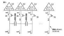
次に、図4、図5、及び図6を用いて読み出し動作中にビット線BLが接地電位に落ちた場合の、該ビット線BLに隣接するビット線BLに接続されたセンス・モジュールの動作について説明する。図5は、本実施形態に係るセンス・モジュール及びビット線を模式的に示した回路図である。図6は、本実施形態に係る半導体装置の充電動作を示すタイミング・チャートである。
<Charge module charging operation>
Next, the operation of the sense module connected to the bit line BL adjacent to the bit line BL when the bit line BL falls to the ground potential during the read operation with reference to FIG. 4, FIG. 5, and FIG. Will be described. FIG. 5 is a circuit diagram schematically showing the sense module and the bit line according to the present embodiment. FIG. 6 is a timing chart showing the charging operation of the semiconductor device according to this embodiment.
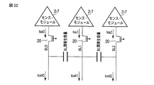
図5に示すように、ビット線BL0とビット線BL1とは互いに隣接し、ビット線BL1とビット線BL2とは互いに隣接し、ビット線BL2とビット線BL3は互いに隣接していない。ビット線BL0がセンス・モジュール2−2から供給される電流をIsa0とし、ビット線BL1がセンス・モジュール2−2から供給される電流をIsa1とし、ビット線BL2がセンス・モジュール2−2から供給される電流をIsa2とし、ビット線BL3がセンス・モジュール2−2から供給される電流をIsa3とする。 As shown in FIG. 5, the bit line BL0 and the bit line BL1 are adjacent to each other, the bit line BL1 and the bit line BL2 are adjacent to each other, and the bit line BL2 and the bit line BL3 are not adjacent to each other. The current supplied from the sense module 2-2 to the bit line BL0 is Isa0, the current supplied from the sense module 2-2 to the bit line BL1 is Isa1, and the bit line BL2 is supplied from the sense module 2-2. The current that is supplied is Isa2, and the current that the bit line BL3 is supplied from the sense module 2-2 is Isa3.
図5、及び図6に示すように、読み出し動作の間に、読み出しの終わったメモリ・セルの属するビット線BL電位を接地電位にする際に、ビット線BL間寄生容量により、隣接するビット線BL(読み出しが終わっていない)の電位が下がる。ビット線BLの電位が下ると、該ビット線BLの電位を所望の電位まで充電する必要がある。 As shown in FIGS. 5 and 6, when the potential of the bit line BL to which the memory cell that has finished reading is set to the ground potential during the read operation, the adjacent bit line is caused by the parasitic capacitance between the bit lines BL. The potential of BL (reading is not finished) drops. When the potential of the bit line BL decreases, it is necessary to charge the potential of the bit line BL to a desired potential.
そのため、時刻t1において、
(1)充電制御回路2−1がBLC0の電位を、例えばBLCと同程度する。これにより、各センス・モジュール2−2のクランプ・トランジスタ2−41がオンとなる。
(2)ビット線BL0、及びビット線BL2の読み出しが終了し、それぞれのセンス・モジュール2−2内のノードN8(INV)が‘H’レベルとなる。これにより、それぞれのプル・ダウン回路によってビット線BL0、BL2の電位がVBLから接地電位まで下げられる。
(3)ビット線BL間の寄生容量により、注目ビット線BL1の電位がVBLから下がる。
(4)図4の加速器2−4に示すように、注目ビット線BL1に隣接するビット線BL0の読み出しが終了し、ビット線BL0に属するセンス・モジュール2−2のINVが‘H’レベルになる。これにより、注目ビット線BL1に属するセンス・モジュール2−2のスイッチ・トランジスタ2−42のゲートにINVLとして、‘H’レベルが与えられる。そのため、該スイッチ・トランジスタ2−42はオンする。また、注目ビット線BL1に隣接するビット線BL2の読み出しが終了し、ビット線BL2に属するセンス・モジュール2−2のINVが‘H’レベルになる。これにより、注目ビット線BL1に属するセンス・モジュール2−2のスイッチ・トランジスタ2−43のゲートにINVRとして、‘H’レベルが与えられる。そのため、該スイッチ・トランジスタ2−43はオンする。これにより、注目ビット線BL1は、従前のクランプ・トランジスタ2−21の電流経路を介する充電に加え、ノードN3、スイッチ・トランジスタ2−42/2−43、クランプ・トランジスタ2−41、ノードN7、及びビット線選択トランジスタ20の電流経路を介して充電を行う。このため、注目ビット線BLの電位は、クランプ・トランジスタ2−21の電流経路のみを用いた場合(破線を参照)に比べ、より早く所望の電位に戻す事が可能である。また、第2のクランプ・トランジスタ2−41のゲートには、第1のクランプ・トランジスタ2−21のゲートへの電位と同程度の電位が印加されているので、加速器2−4は、第1のクランプ・トランジスタ2−21の電流経路の他端に印加される電圧と同等の電圧を出力することができる。
(5)隣接するビット線BLが接地電位にならないビット線BL3は、ビット線BL間寄生容量の影響を受けず、ビット線BLの電位が下がらないため、ビット線BLの充電を行う必要がない。また、ビット線BL3に対して、ビット線BL1と同様の充電をおこなった場合、ビット線が過充電されることになり、過充電分を放電するための時間がビット線リカバリ時間に追加される。このため、ビット線BL3に対する過度な充電は、リカバリ時間をより悪化させることになる。そこで、加速器2−4には、スイッチ・トランジスタ2−42及び2−43が設けられているため、隣接するビット線BLの電位が下がらない場合には、オフしたままとなる。このため、ビット線BL3への過充電(破線を参照)を抑制することができる。
Therefore, at time t1,
(1) The charge control circuit 2-1 sets the potential of BLC0 to the same level as that of BLC, for example. As a result, the clamp transistor 2-41 of each sense module 2-2 is turned on.
(2) Reading of the bit line BL0 and the bit line BL2 is completed, and the node N8 (INV) in each sense module 2-2 becomes the “H” level. Thereby, the potentials of the bit lines BL0 and BL2 are lowered from VBL to the ground potential by the respective pull-down circuits.
(3) Due to the parasitic capacitance between the bit lines BL, the potential of the target bit line BL1 falls from VBL.
(4) As shown in the accelerator 2-4 in FIG. 4, the reading of the bit line BL0 adjacent to the target bit line BL1 is completed, and the INV of the sense module 2-2 belonging to the bit line BL0 is set to the “H” level. Become. As a result, the “H” level is given as INVL to the gate of the switch transistor 2-42 of the sense module 2-2 belonging to the bit line BL1 of interest. Therefore, the switch transistor 2-42 is turned on. Further, the reading of the bit line BL2 adjacent to the target bit line BL1 is completed, and the INV of the sense module 2-2 belonging to the bit line BL2 becomes “H” level. As a result, an “H” level is applied as INVR to the gate of the switch transistor 2-43 of the sense module 2-2 belonging to the bit line BL1 of interest. Therefore, the switch transistor 2-43 is turned on. As a result, the target bit line BL1 is charged with the node N3, the switch transistor 2-42 / 2-43, the clamp transistor 2-41, the node N7, in addition to the charging through the current path of the previous clamp transistor 2-21. In addition, charging is performed through the current path of the bit
(5) The bit line BL3 in which the adjacent bit line BL does not become the ground potential is not affected by the parasitic capacitance between the bit lines BL, and the potential of the bit line BL does not decrease, so that it is not necessary to charge the bit line BL. . Further, when the bit line BL3 is charged in the same manner as the bit line BL1, the bit line is overcharged, and the time for discharging the overcharge is added to the bit line recovery time. . For this reason, excessive charging of the bit line BL3 further deteriorates the recovery time. Therefore, since the accelerator transistors 2-4 are provided with the switch transistors 2-42 and 2-43, they remain off when the potential of the adjacent bit line BL does not drop. For this reason, overcharge (refer to a broken line) to bit line BL3 can be controlled.
時刻t2において、加速器2−4によってビット線BL1の電位が所望の値に戻るので、信号BLC0の電位が下がり、ビット線BL1への充電が終了する。 At time t2, the potential of the bit line BL1 is returned to a desired value by the accelerator 2-4, so that the potential of the signal BLC0 is lowered and the charging of the bit line BL1 is completed.
上述した例では、ビット線BL0及びビット線BL2の読出しが終了した場合について説明したが、図4に示す加速器2−4の構成の場合、注目するビット線BL1に隣接するビット線BL0及びビット線BL2の少なくとも一方だけが、読み出し終了した場合でも、同様の充電動作を行うことができる。 In the above-described example, the case where the reading of the bit line BL0 and the bit line BL2 is completed has been described. However, in the case of the configuration of the accelerator 2-4 illustrated in FIG. The same charging operation can be performed even when at least one of BL2 has finished reading.
<センス・モジュールの効果>
上述した実施形態によれば、不揮発性半導体記憶装置100は、電気的に書き換えが可能なメモリ・セルMCと、メモリ・セルMCのゲートに接続されるワード線WLと、メモリ・セルMCの電流経路の一端に接続されるビット線BLとを備える。また、不揮発性半導体記憶装置100は、電流経路の一端が、ビット線BLと接続される第1のクランプ・トランジスタ2−21と、互いに電気的に接続される第2のクランプ・トランジスタ2−41、及びスイッチ回路(第1のスイッチ・トランジスタ2−42と第2のスイッチ・トランジスタ2−43)を備え、ビット線BL及び第1のクランプ・トランジスタ2−21の電流経路の一端と接続される加速器(電圧制御回路)2−4と、第1のクランプ・トランジスタ2−21の電流経路の他端と、電圧制御回路2−4と接続されるセンス・アンプ2−3とを備える。更に、不揮発性半導体記憶装置100は、センス・アンプ2−3と電気的に接続され、メモリ・セルMCの読み出しを行う前に、第1のデータ(‘L’レベル)を保持し、ビット線BLに所定電流以上の電流が流れた場合は第2のデータ(‘H’レベル)を保持するデータ・ラッチ部2−5と、電流経路の一端が第1のクランプ・トランジスタ2−21の電流経路の他端に接続され、ゲートがデータ・ラッチ部2−5に接続され、データ・ラッチ部2−5に第1のデータが保存された場合、ビット線BLの電位をリセット電位(例えば接地電位、または‘L’レベル)に落とすプル・ダウン回路2−6と、メモリ・セルMCの読み出しを行う際に、ビット線BLに第1のクランプ・トランジスタ2−21のゲート及び第2のクランプ・トランジスタ2−41のゲートに、所定の電位を与える充電制御回路2−1と、を備える。そして、スイッチ・トランジスタ2−42、または2−43のゲートには、それぞれ、ワード線WL方向で隣接する他のデータ・ラッチ部2−5からの信号INVL、INVRが与えられ、ワード線WL方向で隣接する他のデータ・ラッチ部2−5に保持されているデータに依存し、スイッチ・トランジスタ2−42、または2−43がオン、またはオフすることにより、電圧制御回路2−4を介して、ビット線BLとセンス・アンプ2−3との間の接続が制御される。
<Effect of sense module>
According to the embodiment described above, the nonvolatile
また、ワード線WL方向で隣接する少なくとも一つの他のデータ・ラッチ部2−5に第1のデータが保持された場合は、ゲートに第1のデータが与えられるスイッチ・トランジスタ2−42、または2−43がオンする。 When the first data is held in at least one other data latch unit 2-5 adjacent in the word line WL direction, the switch transistor 2-42 to which the first data is applied to the gate, or 2-43 turns on.
ところで、不揮発性半導体記憶装置の読み出し時において、読み出されたビット線BLの電位が接地電位に下げられることがある。そして、ビット線BL間の容量結合により、読み出しの終わっていない隣接するビット線BLの電位が下がる。このように、ビット線BL電位が下がると、再びビット線BLを所望の電位まで充電する必要がある。隣接するビット線BLの読み出しが終了していない(電位が下がっていない)ビット線BLに関しては、ビット線BLの電位が下がっていないため、加速充電を行う必要はない。 By the way, when the nonvolatile semiconductor memory device is read, the potential of the read bit line BL may be lowered to the ground potential. Then, due to capacitive coupling between the bit lines BL, the potential of the adjacent bit line BL that has not been read is lowered. Thus, when the bit line BL potential is lowered, it is necessary to charge the bit line BL again to a desired potential. For bit lines BL that have not been read out of adjacent bit lines BL (potentials are not lowered), the potential of the bit lines BL is not lowered, so that it is not necessary to perform accelerated charging.
上述した実施形態で説明した構成及び動作を用いることで、読み出しが終了し、電位が下げられたビット線BLに隣接し、充電に時間のかかるビット線BLのみ、ビット線BLの充電能力を向上させることができる。 By using the configuration and operation described in the above-described embodiment, the charging capability of the bit line BL is improved only for the bit line BL which is adjacent to the bit line BL whose potential is lowered and the potential is lowered and which takes time to charge. Can be made.
具体的には、互いに隣接するセンス・モジュール2−2において、データ・ラッチ部2−5の、読み出したデータが保持されるノードN8(INV)が、隣接する他のセンス・モジュール2−2の加速器2−4内のスイッチ・トランジスタ2−42または2−43のゲートに接続されている。また、データ・ラッチ部2−5のノードN8は、ビット線BLを接地電位に下げるNMOSトランジスタ2−61のゲートに接続されている。 Specifically, in the adjacent sense modules 2-2, the node N8 (INV) in which the read data is held in the data latch unit 2-5 is connected to the other adjacent sense modules 2-2. It is connected to the gate of the switch transistor 2-42 or 2-43 in the accelerator 2-4. The node N8 of the data latch unit 2-5 is connected to the gate of the NMOS transistor 2-61 that lowers the bit line BL to the ground potential.
つまり、データ・ラッチ部2−5のノードN8が‘H’レベルになると、トランジスタ2−61がオンし、ビット線BLの電位を接地電位に下げる。しかし、ノードN8は、隣接する他のセンス・モジュール2−2の加速器2−4に接続されているため、電位が接地電位に下げられるビット線BLに隣接するビット線BLに加速充電させることが可能となる。また、隣接するビット線BLが接地電位に下げられない場合、加速器2−4はオンしないので、加速充電は行われない。 That is, when the node N8 of the data latch unit 2-5 becomes the “H” level, the transistor 2-61 is turned on and the potential of the bit line BL is lowered to the ground potential. However, since the node N8 is connected to the accelerator 2-4 of another adjacent sense module 2-2, the bit line BL adjacent to the bit line BL whose potential is lowered to the ground potential can be acceleratedly charged. It becomes possible. Further, when the adjacent bit line BL cannot be lowered to the ground potential, the accelerator 2-4 is not turned on, so that accelerated charging is not performed.
このように、上述した実施形態によれば、読み出し時において、隣接するビット線BLが、読み出し終了に起因して電位が下げられる場合でも、ビット線BLを高速に充電することができ、また同時に、隣接するビット線BLの電位が下がらないビット線BLへの過充電を抑制することが可能になる。その結果、ビット線の高速充電を実現し、読み出し特性を向上することが可能な半導体記憶装置を提供することができる。 As described above, according to the above-described embodiment, even when the potential of the adjacent bit line BL is lowered due to the end of reading at the time of reading, the bit line BL can be charged at high speed and at the same time. Thus, it is possible to suppress overcharging to the bit line BL in which the potential of the adjacent bit line BL does not drop. As a result, it is possible to provide a semiconductor memory device capable of realizing high-speed charging of bit lines and improving read characteristics.
(第2の実施形態)
次に、図7を用いて、第2の実施形態に係る加速器(電圧制御回路)2−4の構成について説明する。図7は、第2の実施形態に係る加速器の構成を模式的に示した回路図である。尚、基本的な構成及び基本的な動作は、上述した第1の実施形態と同様である。従って、上述した第1の実施形態で説明した事項及び上述した実施形態から容易に類推可能な事項についての説明は省略する。
(Second Embodiment)
Next, the configuration of an accelerator (voltage control circuit) 2-4 according to the second embodiment will be described with reference to FIG. FIG. 7 is a circuit diagram schematically showing the configuration of the accelerator according to the second embodiment. The basic configuration and basic operation are the same as those in the first embodiment described above. Accordingly, descriptions of the matters described in the first embodiment described above and items that can be easily inferred from the above-described embodiments are omitted.
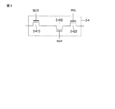
<加速器の構成>
図7に示すように、加速器2−4は、ビット線クランプ用NMOSトランジスタ2−411、2−412、スイッチNMOSトランジスタ2−421、及び2−431を有している。
スイッチ・トランジスタ2−421の電流経路の一端は、ノードN3に接続され、他端は、クランプ・トランジスタ2−411の電流経路の一端に接続される。また、スイッチ・トランジスタ2−421のゲートには、隣接するセンス・モジュール2−2のデータ・ラッチ部2−5からの信号INVLが与えられる。
<Configuration of accelerator>
As shown in FIG. 7, the accelerator 2-4 includes bit line clamping NMOS transistors 2-411 and 412 and switch NMOS transistors 2-421 and 2-431.
One end of the current path of the switch transistor 2-421 is connected to the node N3, and the other end is connected to one end of the current path of the clamp transistor 2-411. The signal INVL from the data latch unit 2-5 of the adjacent sense module 2-2 is applied to the gate of the switch transistor 2-421.
クランプ・トランジスタ2−411の電流経路の一端は、スイッチ・トランジスタ2−421の電流経路の他端に接続され、他端はノードN7に接続されている。クランプ・トランジスタ2−411のゲートには、充電制御回路2−1からの信号BLC0が与えられる。 One end of the current path of the clamp transistor 2-411 is connected to the other end of the current path of the switch transistor 2-421, and the other end is connected to the node N7. A signal BLC0 from the charge control circuit 2-1 is applied to the gate of the clamp transistor 2-411.
スイッチ・トランジスタ2−431の電流経路の一端は、ノードN3に接続され、他端は、クランプ・トランジスタ2−411の電流経路の一端に接続される。また、スイッチ・トランジスタ2−431のゲートには、隣接する他のセンス・モジュール2−2のデータ・ラッチ部2−5からの信号INVRが与えられる。 One end of the current path of the switch transistor 2-431 is connected to the node N3, and the other end is connected to one end of the current path of the clamp transistor 2-411. The signal INVR from the data latch section 2-5 of another adjacent sense module 2-2 is applied to the gate of the switch transistor 2-431.
クランプ・トランジスタ2−412の電流経路の一端は、スイッチ・トランジスタ2−431の電流経路の他端に接続され、他端はノードN7に接続されている。クランプ・トランジスタ2−412のゲートには、充電制御回路2−1からの信号BLC0が与えられる。 One end of the current path of the clamp transistor 2-412 is connected to the other end of the current path of the switch transistor 2-431, and the other end is connected to the node N7. A signal BLC0 from the charge control circuit 2-1 is applied to the gate of the clamp transistor 2-412.
これにより、スイッチ・トランジスタ2−421、及びクランプ・トランジスタ2−411と、スイッチ・トランジスタ2−431、及びクランプ・トランジスタ2−412とは並列接続される。 As a result, the switch transistor 2-421 and the clamp transistor 2-411, and the switch transistor 2-431 and the clamp transistor 2-412 are connected in parallel.
尚、スイッチ・トランジスタ2−421、及びクランプ・トランジスタ2−411と、スイッチ・トランジスタ2−431、及びクランプ・トランジスタ2−412との位置は入れ替えてもかまわない。 Note that the positions of the switch transistor 2-421 and the clamp transistor 2-411, and the switch transistor 2-431 and the clamp transistor 2-412 may be interchanged.
<加速器の動作>
次に、第2の実施形態に係る加速器の読み出し時における充電動作について簡単に説明する。
注目ビット線BLに隣接するビット線BLの読み出しが終了した場合、隣接するビット線BLに属するセンス・モジュール2−2のINVが‘H’レベルになる。これにより、注目ビット線BLに属するセンス・モジュール2−2のスイッチ・トランジスタ2−421のゲートにINVLとして、‘H’レベルが与えられる。そのため、該スイッチ・トランジスタ2−421はオンする。
これにより、注目ビット線BLは、従前のクランプ・トランジスタ2−21の電流経路を介する充電に加え、ノードN3、スイッチ・トランジスタ2−421、クランプ・トランジスタ2−411、ノードN7、及びビット線選択トランジスタ20の電流経路を介して充電を行うことができる。
<Accelerator operation>
Next, a charging operation at the time of reading of the accelerator according to the second embodiment will be briefly described.
When reading of the bit line BL adjacent to the target bit line BL is completed, the INV of the sense module 2-2 belonging to the adjacent bit line BL becomes “H” level. As a result, the “H” level is given as INVL to the gate of the switch transistor 2-421 of the sense module 2-2 belonging to the target bit line BL. Therefore, the switch transistor 2-421 is turned on.
As a result, the target bit line BL is not only charged through the current path of the previous clamp transistor 2-21, but also the node N3, the switch transistor 2-421, the clamp transistor 2-411, the node N7, and the bit line selection. Charging can be performed through the current path of the
また、注目ビット線BLに隣接する他のビット線BLの読み出しが終了した場合、隣接する他のビット線BLに属するセンス・モジュール2−2のINVが‘H’レベルになる。これにより、注目ビット線BLに属するセンス・モジュール2−2のスイッチ・トランジスタ2−431のゲートにINVRとして、‘H’レベルが与えられる。そのため、該スイッチ・トランジスタ2−431はオンする。
これにより、注目ビット線BLは、従前のクランプ・トランジスタ2−21の電流経路を介する充電に加え、ノードN3、スイッチ・トランジスタ2−431、クランプ・トランジスタ2−412、ノードN7、及びビット線選択トランジスタ20の電流経路を介して充電を行うことができる。
In addition, when reading of another bit line BL adjacent to the target bit line BL is completed, INV of the sense module 2-2 belonging to the other adjacent bit line BL becomes “H” level. As a result, the “H” level is given as INVR to the gate of the switch transistor 2-431 of the sense module 2-2 belonging to the target bit line BL. Therefore, the switch transistor 2-431 is turned on.
As a result, the target bit line BL is not only charged through the current path of the previous clamp transistor 2-21, but also the node N3, the switch transistor 2-431, the clamp transistor 2-412, the node N7, and the bit line selection. Charging can be performed through the current path of the
<第2の実施形態の効果>
上述した第2の実施形態によれば、加速器(電圧制御回路)2−4は、電流経路の一端が第2のクランプ・トランジスタ2−411の電流経路の一端に接続され、ゲートに、BLC0が与えられ、第2のクランプ・トランジスタ2−411と接続される第3のクランプ・トランジスタ2−412を更に備え、スイッチ回路は、電流経路の一端が第2のクランプ・トランジスタ2−411の電流経路の他端に接続される第1のスイッチ・トランジスタ2−421、及び電流経路の一端が第3のクランプ・トランジスタ2−412の他端に接続され、電流経路の他端が第1のスイッチ・トランジスタ2−421の他端に接続される第2のスイッチ・トランジスタ2−431を備え、ワード線WL方向で隣接する他のデータ・ラッチ部2−5及び更に他のデータ・ラッチ部2−5に第1のデータが保存されない場合は、第1のスイッチ・トランジスタ2−421及び第2のスイッチ・トランジスタ2−431はオフし、ワード線WL方向で隣接する他のデータ・ラッチ部に第1のデータが保存された場合は、第1のスイッチ・トランジスタ2−421がオンし、ワード線WL方向で隣接する更に他のデータ・ラッチ部に第1のデータが保存された場合は、第2のスイッチ・トランジスタ2−431がオンする。
<Effects of Second Embodiment>
According to the second embodiment described above, in the accelerator (voltage control circuit) 2-4, one end of the current path is connected to one end of the current path of the second clamp transistor 2-411, and BLC0 is connected to the gate. A third clamp transistor 2-412 provided and connected to the second clamp transistor 2-411, wherein the switch circuit has one end of the current path of the second clamp transistor 2-411. Is connected to the other end of the third clamp transistor 2-412, and the other end of the current path is connected to the first switch transistor 2-421. The second switch transistor 2-431 is connected to the other end of the transistor 2-421, and another data latch unit 2-5 adjacent to the word line WL in the direction of the word line WL When the first data is not stored in the other data latch unit 2-5, the first switch transistor 2-421 and the second switch transistor 2-431 are turned off and are adjacent in the word line WL direction. When the first data is stored in the other data latch unit, the first switch transistor 2-421 is turned on, and the first data is stored in the other data latch unit adjacent in the word line WL direction. Is stored, the second switch transistor 2-431 is turned on.
このように、加速器2−4は、スイッチ・トランジスタ2−421、及びクランプ・トランジスタ2−411を経由する充電経路と、スイッチ・トランジスタ2−431、及びクランプ・トランジスタ2−412とを経由する充電経路とを有している。両側のビット線が読み出し終了した場合、隣接ビット線による影響が大きく、より多い充電を必要とし、読み出し終了したビット線が片側の場合、隣接ビット線による影響が小さく、充電量は少なくて済む。第2の実施形態では、第1の実施形態で説明した加速器2−4に比べて充電経路が多い。このため、注目ビット線BLに隣接するビット線、及び隣接する他のビット線(両側のビット線)の読み出しが終了した場合、注目ビット線BLの電位を、第1の実施形態よりも早く所望の電位に戻す事が可能である。また、隣接するビット線の片側のみが読み出し修了した場合は、充電能力を絞り、不要な過充電をすることなく、適切に注目ビット線BLを充電することができる。 As described above, the accelerator 2-4 is charged via the charging path via the switch transistor 2-421 and the clamp transistor 2-411, and the charging via the switch transistor 2-431 and the clamp transistor 2-412. And has a route. When the bit lines on both sides are completely read, the influence of the adjacent bit lines is large and more charging is required. When the bit line whose reading is completed is one side, the influence of the adjacent bit lines is small and the amount of charging is small. In the second embodiment, there are more charging paths than the accelerator 2-4 described in the first embodiment. Therefore, when the reading of the bit line adjacent to the target bit line BL and the other adjacent bit lines (the bit lines on both sides) is completed, the potential of the target bit line BL is desired earlier than in the first embodiment. It is possible to return to the potential. In addition, when only one side of the adjacent bit line is read, the charging capability is reduced, and the target bit line BL can be appropriately charged without unnecessary overcharging.
(第3の実施形態)
次に、図8を用いて、第3の実施形態に係る加速器(電圧制御回路)2−4の構成について説明する。図8は、第3の実施形態に係る加速器の構成を模式的に示した回路図である。尚、基本的な構成及び基本的な動作は、上述した第1の実施形態と同様である。従って、上述した第1の実施形態で説明した事項及び上述した実施形態から容易に類推可能な事項についての説明は省略する。
(Third embodiment)
Next, the configuration of the accelerator (voltage control circuit) 2-4 according to the third embodiment will be described with reference to FIG. FIG. 8 is a circuit diagram schematically showing the configuration of the accelerator according to the third embodiment. The basic configuration and basic operation are the same as those in the first embodiment described above. Accordingly, descriptions of the matters described in the first embodiment described above and items that can be easily inferred from the above-described embodiments are omitted.
<加速器の構成>
図8に示すように、加速器2−4は、ビット線クランプ用NMOSトランジスタ2−413、スイッチNMOSトランジスタ2−422、及び2−432を有している。
スイッチ・トランジスタ2−422の電流経路の一端は、ノードN3に接続され、他端は、スイッチ・トランジスタ2−432の電流経路の一端に接続される。また、スイッチ・トランジスタ2−422のゲートには、隣接するセンス・モジュール2−2のデータ・ラッチ部2−5からの信号INVLが与えられる。
<Configuration of accelerator>
As shown in FIG. 8, the accelerator 2-4 includes a bit line clamping NMOS transistor 2-413, and switch NMOS transistors 2-422 and 2-432.
One end of the current path of the switch transistor 2-422 is connected to the node N3, and the other end is connected to one end of the current path of the switch transistor 2-432. The signal INVL from the data latch unit 2-5 of the adjacent sense module 2-2 is applied to the gate of the switch transistor 2-422.
スイッチ・トランジスタ2−432の電流経路の一端は、スイッチ・トランジスタ2−422の他端に接続され、他端はクランプ・トランジスタ2−413の電流経路の一端に接続される。また、スイッチ・トランジスタ2−432のゲートには、隣接する他のセンス・モジュール2−2のデータ・ラッチ部2−5からの信号INVRが与えられる。 One end of the current path of the switch transistor 2-432 is connected to the other end of the switch transistor 2-422, and the other end is connected to one end of the current path of the clamp transistor 2-413. The signal INVR from the data latch section 2-5 of another adjacent sense module 2-2 is applied to the gate of the switch transistor 2-432.
クランプ・トランジスタ2−413の電流経路の一端は、スイッチ・トランジスタ2−432の電流経路の他端に接続され、他端はノードN7に接続される。クランプ・トランジスタ2−413のゲートには、充電制御回路2−1からの信号BLC0が与えられる。 One end of the current path of the clamp transistor 2-413 is connected to the other end of the current path of the switch transistor 2-432, and the other end is connected to the node N7. A signal BLC0 from the charge control circuit 2-1 is applied to the gate of the clamp transistor 2-413.
これにより、スイッチ・トランジスタ2−422、スイッチ・トランジスタ2−432、及びクランプ・トランジスタ2−413とは直列接続される。 As a result, the switch transistor 2-422, the switch transistor 2-432, and the clamp transistor 2-413 are connected in series.
尚、スイッチ・トランジスタ2−422、及び2−432と、クランプ・トランジスタ2−413との位置は入れ替えてもかまわない。 Note that the positions of the switch transistors 2-422 and 2-432 and the clamp transistors 2-413 may be interchanged.
<加速器の動作>
次に、第3の実施形態に係る加速器の読み出し時における充電動作について簡単に説明する。
注目ビット線BLに隣接するビット線BLの読み出しが終了した場合、隣接するビット線BLに属するセンス・モジュール2−2のINVが‘H’レベルになる。これにより、注目ビット線BLに属するセンス・モジュール2−2のスイッチ・トランジスタ2−422のゲートにINVLとして、‘H’レベルが与えられる。そのため、該スイッチ・トランジスタ2−422はオンする。
また、注目ビット線BLに隣接する他のビット線BLの読み出しが終了した場合、隣接する他のビット線BLに属するセンス・モジュール2−2のINVが‘H’レベルになる。これにより、注目ビット線BLに属するセンス・モジュール2−2のスイッチ・トランジスタ2−432のゲートにINVRとして、‘H’レベルが与えられる。そのため、該スイッチ・トランジスタ2−432はオンする。
これにより、注目ビット線BLは、従前のクランプ・トランジスタ2−21の電流経路を介する充電に加え、ノードN3、スイッチ・トランジスタ2−422、スイッチ・トランジスタ2−432、クランプ・トランジスタ2−413、ノードN7、及びビット線選択トランジスタ20の電流経路を介して充電を行うことができる。
<Accelerator operation>
Next, the charging operation at the time of reading of the accelerator according to the third embodiment will be briefly described.
When reading of the bit line BL adjacent to the target bit line BL is completed, the INV of the sense module 2-2 belonging to the adjacent bit line BL becomes “H” level. As a result, an “H” level is given as INVL to the gate of the switch transistor 2-422 of the sense module 2-2 belonging to the target bit line BL. Therefore, the switch transistor 2-422 is turned on.
In addition, when reading of another bit line BL adjacent to the target bit line BL is completed, INV of the sense module 2-2 belonging to the other adjacent bit line BL becomes “H” level. As a result, the gate of the switch transistor 2-432 of the sense module 2-2 belonging to the target bit line BL is given “H” level as INVR. Therefore, the switch transistor 2-432 is turned on.
Thus, the target bit line BL is not only charged through the current path of the previous clamp transistor 2-21, but also the node N3, the switch transistor 2-422, the switch transistor 2-432, the clamp transistor 2-413, Charging can be performed through the current path of the node N7 and the bit
<第3の実施形態の効果>
上述した第3の実施形態によれば、ワード線WL方向で隣接する他の二つのデータ・ラッチ部2−5に第1のデータが保存された場合は、スイッチ回路がオンする。
<Effect of the third embodiment>
According to the third embodiment described above, when the first data is stored in the other two data latch units 2-5 adjacent in the word line WL direction, the switch circuit is turned on.
このように、加速器2−4では、スイッチ・トランジスタ2−422、及びスイッチ・トランジスタ2−432が直列に接続されている。このため、注目ビット線BLに隣接するビット線、及び隣接する他のビット線(両側のビット線)の読み出しが終了した場合にのみ、注目ビット線BLへの加速充電を行う。そして、片側のビット線の読み出しのみが終了した場合には、注目ビット線BLへの充電は行わない。これは、注目ビット線BLに隣接する両側のビット線BLのうち、片側のビット線BLからのビット線BL間寄生容量の影響は少なく、加速充電を行うと、過充電になる可能性がある場合に有効である。 In this manner, in the accelerator 2-4, the switch transistor 2-422 and the switch transistor 2-432 are connected in series. For this reason, accelerated charging of the target bit line BL is performed only when reading of the bit line adjacent to the target bit line BL and other adjacent bit lines (bit lines on both sides) is completed. Then, when only reading of the bit line on one side is completed, the target bit line BL is not charged. This is because the bit line BL on one side of the bit line BL adjacent to the target bit line BL is less affected by the parasitic capacitance between the bit lines BL, and may be overcharged when accelerated charging is performed. It is effective in the case.
(第4の実施形態)
次に、図9を用いて、第4の実施形態に係る加速器2−4の構成について説明する。図9は、第4の実施形態に係る加速器の構成を模式的に示した回路図である。尚、基本的な構成及び基本的な動作は、上述した第1の実施形態と同様である。従って、上述した第1の実施形態で説明した事項及び上述した実施形態から容易に類推可能な事項についての説明は省略する。
(Fourth embodiment)
Next, the structure of the accelerator 2-4 which concerns on 4th Embodiment is demonstrated using FIG. FIG. 9 is a circuit diagram schematically showing the configuration of the accelerator according to the fourth embodiment. The basic configuration and basic operation are the same as those in the first embodiment described above. Accordingly, descriptions of the matters described in the first embodiment described above and items that can be easily inferred from the above-described embodiments are omitted.
<加速器の構成>
図9に示すように、加速器2−4は、ビット線クランプ用NMOSトランジスタ2−414、スイッチNMOSトランジスタ2−423、及び2−433を有している。
クランプ・トランジスタ2−414の電流経路の一端は、ノードN2に接続され、他端はノードN12に接続される。クランプ・トランジスタ2−414のゲートには、充電制御回路2−1からの信号BLC0が与えられる。
<Configuration of accelerator>
As shown in FIG. 9, the accelerator 2-4 includes a bit line clamping NMOS transistor 2-414, switch NMOS transistors 2-423, and 2-433.
One end of the current path of the clamp transistor 2-414 is connected to the
スイッチ・トランジスタ2−423の電流経路の一端は、ノードN12に接続され、他端は、ノードN7に接続される。また、スイッチ・トランジスタ2−423のゲートには、隣接するセンス・モジュール2−2のデータ・ラッチ部2−5からの信号INVLが与えられる。 One end of the current path of the switch transistor 2-423 is connected to the node N12, and the other end is connected to the node N7. The signal INVL from the data latch unit 2-5 of the adjacent sense module 2-2 is applied to the gate of the switch transistor 2-423.
スイッチ・トランジスタ2−433の電流経路の一端は、ノードN12に接続され、他端はノードN7に接続される。また、スイッチ・トランジスタ2−433のゲートには、隣接する他のセンス・モジュール2−2のデータ・ラッチ部2−5からの信号INVRが与えられる。 One end of the current path of the switch transistor 2-433 is connected to the node N12, and the other end is connected to the node N7. The signal INVR from the data latch section 2-5 of another adjacent sense module 2-2 is applied to the gate of the switch transistor 2-433.
<加速器の動作>
次に、第4の実施形態に係る加速器の読み出し時における充電動作について簡単に説明する。
スイッチ・トランジスタ2−423は、第1の実施形態で説明したスイッチ・トランジスタ2−42と同様に動作し、スイッチ・トランジスタ2−433は、第1の実施形態で説明したスイッチ・トランジスタ2−433と同様に動作する。また、クランプ・トランジスタ2−414は、第1の実施形態で説明したクランプ・トランジスタ2−41と同様に動作する。
これにより、注目ビット線BLは、従前のクランプ・トランジスタ2−21の電流経路を介する充電に加え、ノードN2、クランプ・トランジスタ2−414、スイッチ・トランジスタ2−423、スイッチ・トランジスタ2−433、ノードN7、及びビット線選択トランジスタ20の電流経路を介して充電を行うことができる。
<Accelerator operation>
Next, a charging operation at the time of reading of the accelerator according to the fourth embodiment will be briefly described.
The switch transistor 2-423 operates in the same manner as the switch transistor 2-42 described in the first embodiment, and the switch transistor 2-433 is the switch transistor 2-433 described in the first embodiment. Works as well. The clamp transistor 2-414 operates in the same manner as the clamp transistor 2-41 described in the first embodiment.
As a result, the target bit line BL is not only charged through the current path of the previous clamp transistor 2-21, but also the node N2, the clamp transistor 2-414, the switch transistor 2-423, the switch transistor 2-433, Charging can be performed through the current path of the node N7 and the bit
<第4の実施形態の効果>
上述した第4の実施形態によれば、加速器2−4の一端は、電源電圧VDDが供給されるノードに接続され、他端はノードN7に接続されている。このように、加速器2−4の一端を、ノードN2に接続することで、NMOSトランジスタ2−414のドレイン・ソース間電位が、上述した各実施形態の加速器よりも大きくなるため、より大きな充電電流をビット線BLに供給することが可能である。
<Effect of the fourth embodiment>
According to the fourth embodiment described above, one end of the accelerator 2-4 is connected to the node to which the power supply voltage VDD is supplied, and the other end is connected to the node N7. In this way, by connecting one end of the accelerator 2-4 to the node N2, the drain-source potential of the NMOS transistor 2-414 becomes larger than that of the accelerator according to each of the embodiments described above, and therefore a larger charging current. Can be supplied to the bit line BL.
(第5の実施形態)
次に、図10を用いて、第5の実施形態に係る加速器2−4の構成について説明する。図10は、第5の実施形態に係る加速器の構成を模式的に示した回路図である。尚、基本的な構成及び基本的な動作は、上述した第1の実施形態と同様である。従って、上述した第1の実施形態で説明した事項及び上述した実施形態から容易に類推可能な事項についての説明は省略する。
(Fifth embodiment)
Next, the structure of the accelerator 2-4 which concerns on 5th Embodiment is demonstrated using FIG. FIG. 10 is a circuit diagram schematically showing the configuration of the accelerator according to the fifth embodiment. The basic configuration and basic operation are the same as those in the first embodiment described above. Accordingly, descriptions of the matters described in the first embodiment described above and items that can be easily inferred from the above-described embodiments are omitted.
<加速器の構成>
図10に示すように、加速器2−4は、ビット線クランプ用NMOSトランジスタ2−415、スイッチPMOSトランジスタ(スイッチ・トランジスタとも呼ぶ)2−424、及び2−434を有している。
スイッチ・トランジスタ2−424の電流経路の一端は、ノードN2に接続され、他端は、ノードN13に接続される。また、スイッチ・トランジスタ2−424のゲートには、隣接するセンス・モジュール2−2のデータ・ラッチ部2−5のノードN11に接続され、信号LATLが与えられる。
<Configuration of accelerator>
As shown in FIG. 10, the accelerator 2-4 includes bit line clamping NMOS transistors 2-415, switch PMOS transistors (also referred to as switch transistors) 2-424, and 2-434.
One end of the current path of the switch transistor 2-424 is connected to the
スイッチ・トランジスタ2−434の電流経路の一端は、ノードN2に接続され、他端は、ノードN13に接続される。また、スイッチ・トランジスタ2−434のゲートには、隣接する他のセンス・モジュール2−2のデータ・ラッチ部2−5のノードN11に接続され、信号LATRが与えられる。
One end of the current path of the switch transistor 2-434 is connected to the node N2, and the other end is connected to the node N13. Further, the gate of the switch transistor 2-434 is connected to the
クランプ・トランジスタ2−415の電流経路の一端は、ノードN13に接続され、他端はノードN7に接続される。クランプ・トランジスタ2−415のゲートには、充電制御回路2−1からの信号BLC0が与えられる。
One end of the current path of the clamp transistor 2-415 is connected to the node N 13 and the other end is connected to the
<加速器の動作>
次に、第5の実施形態に係る加速器の読み出し時における充電動作について簡単に説明する。
スイッチ・トランジスタ2−424は、第4の実施形態で説明したスイッチ・トランジスタ2−423のN型をP型に変更し、ゲートにLAT(ノードN11)Lが与えられているものである。また、スイッチ・トランジスタ2−434は、第4の実施形態で説明したスイッチ・トランジスタ2−433のN型をP型に変更し、ゲートにLAT(ノードN11)Lが与えられているものである。ここで、第4の実施形態で説明したように、INV(ノードN8)が‘H’レベルの場合は、LAT(ノードN11)は‘L’レベルであり、INV(ノードN8)が‘L’レベルの場合は、LAT(ノードN11)は‘H’レベルであるという関係がある。このため、ゲートにINVの替わりにLATが与えられるスイッチ・トランジスタ2−424はスイッチ・トランジスタ2−423と同様に動作し、スイッチ・トランジスタ2−434はスイッチ・トランジスタ2−433と同様に動作する。
<Accelerator operation>
Next, a charging operation at the time of reading of the accelerator according to the fifth embodiment will be briefly described.
In the switch transistor 2-424, the N type of the switch transistor 2-423 described in the fourth embodiment is changed to a P type, and the gate is provided with LAT (node N 11) L. The switch transistor 2-434 is obtained by changing the N type of the switch transistor 2-433 described in the fourth embodiment to a P type and is provided with LAT (node N 11) L at the gate. . Here, as described in the fourth embodiment, when INV (node N8) is at “H” level, LAT (node N11) is at “L” level, and INV (node N8) is at “L”. In the case of the level, there is a relationship that the LAT (node N11) is at the “H” level. For this reason, the switch transistor 2-424 in which LAT is given to the gate instead of INV operates in the same manner as the switch transistor 2-423, and the switch transistor 2-434 operates in the same manner as the switch transistor 2-433. .
これにより、注目ビット線BLは、従前のクランプ・トランジスタ2−21の電流経路を介する充電に加え、ノードN2、スイッチ・トランジスタ2−424/2−434、ノードN13、クランプ・トランジスタ2−415、ノードN7、及びビット線選択トランジスタ20の電流経路を介して充電を行うことができる。
As a result, the target bit line BL is not only charged through the current path of the previous clamp transistor 2-21, but also the node N2, the switch transistors 2-424 / 2-434, the node N13, the clamp transistors 2-415, Charging can be performed through the current path of the node N7 and the bit
<第5の実施形態の効果>
上述した第5の実施形態によれば、加速器2−4の一端は、電源電圧VDDが供給されるノードに接続され、他端はノードN7に接続されている。また、スイッチ・トランジスタ2−424及び2−434として、PMOSトランジスタを用いているので、NMOSトランジスタに比べて電圧VDDを流しやすい。このように、加速器2−4の一端を、ノードN2に接続することで、NMOSトランジスタ2−414のドレイン・ソース間電位が、上述した各実施形態の加速器よりも大きくなるため、より大きな充電電流をビット線BLに供給することが可能である。
<Effect of Fifth Embodiment>
According to the fifth embodiment described above, one end of the accelerator 2-4 is connected to the node to which the power supply voltage VDD is supplied, and the other end is connected to the node N7. In addition, since the PMOS transistors are used as the switch transistors 2-424 and 2-434, the voltage VDD is more likely to flow than the NMOS transistors. In this way, by connecting one end of the accelerator 2-4 to the node N2, the drain-source potential of the NMOS transistor 2-414 becomes larger than that of the accelerator according to each of the embodiments described above, and therefore a larger charging current. Can be supplied to the bit line BL.
(第6の実施形態)
次に、図11、及び図12を用いて、第6の実施形態に係る半導体装置の読み出し動作を説明する。図11は、第6の実施形態に係るメモリ・セルの閾値分布図である。図12は、第6の実施形態に係る半導体装置の読み出し動作を示すフローチャートであり、(a)は下位ビットの読み出し、(b)は上位ビットの読み出しのフローチャートである。尚、基本的な構成及び基本的な動作は、上述した第1の実施形態と同様である。従って、上述した第1の実施形態で説明した事項及び上述した実施形態から容易に類推可能な事項についての説明は省略する。
(Sixth embodiment)
Next, a read operation of the semiconductor device according to the sixth embodiment will be described with reference to FIGS. 11 and 12. FIG. 11 is a threshold distribution diagram of a memory cell according to the sixth embodiment. FIG. 12 is a flowchart showing the read operation of the semiconductor device according to the sixth embodiment, where (a) is a lower bit read and (b) is a higher bit read flowchart. The basic configuration and basic operation are the same as those in the first embodiment described above. Accordingly, descriptions of the matters described in the first embodiment described above and items that can be easily inferred from the above-described embodiments are omitted.
一つのメモリ・セルに2bit以上のデータを記憶する多値メモリ・セルでは、データの読み出しにおいて、読み出しレベルを変えた2回以上の読み出しにより、データの判定が行われる。ここでは、4レベルのデータを記憶するメモリ・セルの場合について説明する。 In a multi-level memory cell that stores data of 2 bits or more in one memory cell, the data is determined by reading two or more times while changing the reading level. Here, a case of a memory cell storing four levels of data will be described.
図11に示すように、メモリ・セルは、4つのレベルに対応する4つの閾値分布を持ち、各レベルは、上位ビット及び下位ビットの2ビットのアドレスをもつ。ここでは、閾値の低いものから、11、01、00、10と番号付けをし、左側の数字を上位ビット、右側の数字を下位ビットに割り当てる。また、それぞれのレベルを判定するための読み出し電圧レベルをそれぞれVg1、Vg2、及びVg3と書く。これは、読み出し動作において、ワード線WLに印加される電圧である。 As shown in FIG. 11, the memory cell has four threshold distributions corresponding to the four levels, and each level has a 2-bit address of an upper bit and a lower bit. Here, the numbers are assigned as 11, 01, 00, 10 from the lowest threshold, and the left number is assigned to the upper bit and the right number is assigned to the lower bit. The read voltage levels for determining the respective levels are written as Vg1, Vg2, and Vg3, respectively. This is a voltage applied to the word line WL in the read operation.
ワード線WLに読み出し電圧レベルを印加し、セルを流れるセル電流Icellが、参照電流Irefより大きい場合は、Data“1”と判断され、小さい場合は、Data“0”と判断される。この多値メモリ・セルの読み出し動作は、図12を参照するように行われる。 When the read voltage level is applied to the word line WL and the cell current Icell flowing through the cell is larger than the reference current Iref, it is determined as Data “1”, and when it is smaller, it is determined as Data “0”. This multilevel memory cell read operation is performed with reference to FIG.
<下位ビットの読み出し(図12(a)参照)>
(ステップS101)
読み出しレベルとして、ワード線WLにVg2を設定することで、下位ビットの読み出しができる。
<Reading of lower bits (see FIG. 12A)>
(Step S101)
By setting Vg2 to the word line WL as a read level, lower bits can be read.
(ステップS102)
ワード線WLの電圧レベルをVg2に設定した時、メモリ・セルを流れる電流Icellが参照電流Irefより大きい場合(Icell>Iref)は、下位ビットは“1”となる。また、メモリ・セルを流れる電流Icellが参照電流Irefより大きくない場合(Icell<Iref)は、下位ビットは“0”となる。このようにして、下位ビットのデータの判定ができる。
(Step S102)
When the voltage level of the word line WL is set to Vg2, if the current Icell flowing through the memory cell is larger than the reference current Iref (Icell> Iref), the lower bit is “1”. When the current Icell flowing through the memory cell is not larger than the reference current Iref (Icell <Iref), the lower bit is “0”. In this way, the lower bit data can be determined.
<上位ビットの読み出し(図12(b)参照)>
上位ビットのデータを知るためには、Vg1、及びVg3の二つのレベルで読み出しを行い、その結果でデータの“0”/“1”の判断を行う。
<Reading of upper bits (see FIG. 12B)>
In order to know the upper bit data, reading is performed at two levels of Vg1 and Vg3, and “0” / “1” of the data is determined based on the result.
(ステップS201)
まず、ワード線WLに、読み出しレベルとしてVg1を設定し、上位ビットの読み出しを行う。
(Step S201)
First, Vg1 is set as the read level for the word line WL, and the upper bits are read.
(ステップS202)
このとき、セル電流Icellが参照電流Irefよりも大きい場合(Icell>Iref)は、上位ビットは“1”となり、読み出しが終了する。セル電流Icellが参照電流Irefよりも大きくない場合(Icell<Iref)は、ステップS203に進む。
(Step S202)
At this time, when the cell current Icell is larger than the reference current Iref (Icell> Iref), the upper bit is “1” and the reading is completed. When the cell current Icell is not larger than the reference current Iref (Icell <Iref), the process proceeds to step S203.
(ステップS203)
次に、ワード線WLに、読み出しレベルとしてVg3を設定し、再度読み出しを行う。
(Step S203)
Next, Vg3 is set as a read level for the word line WL, and read is performed again.
(ステップS204)
このとき、セル電流Icellが参照電流Irefよりも小さい場合(Icell<Iref)は、上位ビットは“1”と判定され、読み出しが終了する。また、セル電流Icellが参照電流Irefよりも小さくない場合(Icell>Iref)は、上位ビットは“0”と判定され、読み出しが終了する。なお、この判定は、センス・アンプのデータを取り出すことにより、外の回路で行われる。
(Step S204)
At this time, when the cell current Icell is smaller than the reference current Iref (Icell <Iref), the upper bit is determined to be “1”, and the reading ends. If the cell current Icell is not smaller than the reference current Iref (Icell> Iref), the upper bit is determined to be “0”, and the reading is completed. This determination is performed by an external circuit by extracting the data of the sense amplifier.
上述したように、複数のメモリ・セルを同時に読み出す不揮発性半導体記憶装置において、上位ビットの読み出しでは、複数回の読み出し動作を行うが、1回目の読み出しで、上位データ(または下位データ)が“1”と判定されたセルに対して、2回目の読み出しを行う必要がない。このため、そのようなメモリ・セルが接続されるビット線BLは、2回目の読み出し時は、ソース線と同電位が印加される(ソース線に流れるセル電流を減らして、ソース線電圧の浮きを抑制)。 As described above, in the nonvolatile semiconductor memory device that reads a plurality of memory cells at the same time, in the upper bit read, a plurality of read operations are performed, but in the first read, the upper data (or lower data) is “ There is no need to perform the second read for the cell determined as 1 ″. For this reason, the bit line BL to which such a memory cell is connected is applied with the same potential as that of the source line at the time of the second read (the cell current flowing in the source line is reduced, and the source line voltage is floated). Suppression).
第1の実施形態と同様に、1回目と2回目の読み出しの際、読み出しが終了したメモリ・セルのビット線BLを接地電位にする。このため、第1の実施形態で説明した例と同様に、2回目の読み出しを行うビット線BLに隣接するビット線BLの電位が接地電位に下がった場合、ビット線間の容量結合により、2回目の読み出しを行うビット線BLへのディスターブが起こる場合がある。 As in the first embodiment, at the time of the first and second reading, the bit line BL of the memory cell that has been read is set to the ground potential. For this reason, as in the example described in the first embodiment, when the potential of the bit line BL adjacent to the bit line BL to be read for the second time falls to the ground potential, the capacitance coupling between the bit lines causes 2 There is a case where disturbance to the bit line BL to be read a second time occurs.
しかし、このような多値メモリ・セルの読み出し動作においても、上述した各実施形態と同様の構成及び動作を有する不揮発性半導体記憶装置を用いることで、上述した各実施形態で説明したものと同様の効果を得ることができる。つまり、ビット線BLを高速に充電することができ、また同時に、隣接するビット線BLの電位が下がらないビット線BLへの過充電を抑制することが可能になる。 However, the read operation of such a multilevel memory cell is the same as that described in each of the above embodiments by using a nonvolatile semiconductor memory device having the same configuration and operation as each of the above embodiments. The effect of can be obtained. That is, the bit line BL can be charged at a high speed, and at the same time, overcharging to the bit line BL in which the potential of the adjacent bit line BL does not drop can be suppressed.
(第7の実施形態)
次に、3次元構造を有する不揮発性半導体記憶装置に、第1〜第6の実施形態で説明したセンス・モジュールを配置する方法について説明する。また、第7の実施形態では3次元積層構造の半導体集積回路の一例を説明する。
(Seventh embodiment)
Next, a method for arranging the sense modules described in the first to sixth embodiments in a nonvolatile semiconductor memory device having a three-dimensional structure will be described. In the seventh embodiment, an example of a semiconductor integrated circuit having a three-dimensional stacked structure will be described.
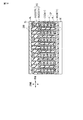
<三次元積層構造の半導体集積回路の概要>
三次元積層構造の半導体集積回路では、半導体基板上に導電性ポリシリコンから構成される複数の導電層を積み重ねて三次元化を図る。一般的なNANDフラッシュ・メモリを三次元積層構造の半導体集積回路に適用した場合(以下、3次元積層NANDフラッシュ・メモリと称すことがある)、メモリ・セル・アレイは三次元化されるが、周辺回路は二次元構造のままである。
<Outline of three-dimensional stacked semiconductor integrated circuit>
In a semiconductor integrated circuit having a three-dimensional stacked structure, a plurality of conductive layers made of conductive polysilicon are stacked on a semiconductor substrate to achieve a three-dimensional structure. When a general NAND flash memory is applied to a semiconductor integrated circuit having a three-dimensional stacked structure (hereinafter sometimes referred to as a three-dimensional stacked NAND flash memory), the memory cell array is three-dimensionalized. The peripheral circuit remains a two-dimensional structure.
<三次元積層構造の半導体集積回路の基本構造>
まず、図13を用いて三次元積層NANDフラッシュ・メモリの基本構造について説明する。図13は、三次元積層NANDフラッシュ・メモリの鳥瞰図を示している。
<Basic structure of three-dimensional stacked semiconductor integrated circuit>
First, the basic structure of a three-dimensional stacked NAND flash memory will be described with reference to FIG. FIG. 13 shows a bird's eye view of a three-dimensional stacked NAND flash memory.
図13に示すように、不揮発性半導体記憶装置(三次元積層NANDフラッシュ・メモリ)100は、メモリ・セル・トランジスタ領域12、複数のワード線WL、複数の選択ゲートSG、複数のソース線SL、およびバック・ゲートBG等を備えている。図示していないが、制御回路は、ワード線駆動回路、選択ゲート駆動回路、ソース線駆動回路、ビット線制御回路及びバック・ゲート・トランジスタ駆動回路等によって構成されている。
As shown in FIG. 13, the nonvolatile semiconductor memory device (three-dimensional stacked NAND flash memory) 100 includes a memory
なお、図13におけるメモリ・セル・トランジスタ領域12は、上述したメモリ・セル・アレイとほぼ同義である。本実施形態の一例として、制御回路は、メモリ・セル・トランジスタ領域12(メモリ・セル・アレイ)の外側に配置されている。
Note that the memory
メモリ・セル・トランジスタ領域12には、複数のワード線WL、複数のビット線BL、複数のソース線SL、バック・ゲートBG、および複数の選択ゲートSGが設けられている。このメモリ・セル・トランジスタ領域12において、積層された複数のワード線WLと後述するU字状シリコン・ピラーSPとの各交差位置に、データを記憶するメモリ・セル・トランジスタが配置されている。なお、図13において、ワード線WLが4層積層された例を示しているが、これに限らない。
ワード線駆動回路(不図示)は、ワード線WLに接続され、ワード線WLに印加する電圧を制御する。また、ワード線駆動回路とワード線WLとを接続する配線は全て、同レベルの配線層に形成されているが、これに限らず、異なるレベルの配線層に形成されていてもよい。また、図示せぬビット線駆動回路は、ビット線BLに印加する電圧を制御する。
ソース線駆動回路(不図示)は、ソース線SLに接続され、ソース線SLに印加する電圧を制御する。このソース線駆動回路は、全てのソース線SLに接続されているが、これに限らず、各ソース線SLに1つずつ設けられていてもよい。
バック・ゲート駆動回路(不図示)は、バック・ゲートBGに接続され、バック・ゲートBGに印加する電圧を制御する。
選択ゲート駆動回路(不図示)は、選択ゲートSGに接続され、選択ゲートSGに印加する電圧を制御する。
In the memory
A word line driving circuit (not shown) is connected to the word line WL and controls a voltage applied to the word line WL. Further, all the wirings connecting the word line driving circuit and the word lines WL are formed in the wiring layer of the same level, but not limited to this, they may be formed in wiring layers of different levels. A bit line driving circuit (not shown) controls the voltage applied to the bit line BL.
A source line driver circuit (not shown) is connected to the source line SL and controls a voltage applied to the source line SL. This source line driving circuit is connected to all the source lines SL, but is not limited to this, and one source line driving circuit may be provided for each source line SL.
The back gate drive circuit (not shown) is connected to the back gate BG and controls the voltage applied to the back gate BG.
The selection gate drive circuit (not shown) is connected to the selection gate SG and controls the voltage applied to the selection gate SG.
図14は、図13に示すメモリ・セル・トランジスタ領域12のカラム(Y)方向に沿った断面図であり、第7の実施形態におけるメモリ・セル・トランジスタ領域12の構造を示している。図15は、図14に示すNANDストリングの拡大図を示している。
FIG. 14 is a cross-sectional view taken along the column (Y) direction of the memory
図14に示すように、メモリ・セル・トランジスタ領域12において、基板30上に、U字状シリコン・ピラーSPで構成される複数のNANDストリング(メモリ・セル・ストリング)200が形成されている。各NANDストリング200は、複数のメモリ・セル・トランジスタMTr、およびその両端に形成された2つの選択トランジスタ(ドレイン側選択トランジスタSDTrおよびソース側選択トランジスタSSTr)を有している。
As shown in FIG. 14, in the memory
複数のメモリ・セル・トランジスタMTrは、U字状シリコン・ピラーSPと複数のコントロール・ゲートCG(ワード線WL)との各交差位置に形成され、電流経路が直列に接続されている。 The plurality of memory cell transistors MTr are formed at each intersection position of the U-shaped silicon pillar SP and the plurality of control gates CG (word lines WL), and current paths are connected in series.
図15に示すように、各メモリ・セル・トランジスタMTrは、U字状シリコン・ピラーSPとコントロール・ゲートCGとの間に、メモリ膜324を有している。このメモリ膜324は、U字状シリコン・ピラーSPの周囲に順に形成されたトンネル絶縁膜322、電荷蓄積層321、およびブロック絶縁膜320で構成されている。すなわち、各メモリ・セル・トランジスタMTrは、MONOS構造を有している。MONOS構造とは、電荷蓄積層が窒化物(nitride)などの絶縁体から構成されるメモリ・セル構造のことである。ここでは、電荷蓄積層は、多層構造(Charge trap layers)とし、ONO(oxide/nitride/oxide)の例を挙げる。
As shown in FIG. 15, each memory cell transistor MTr includes a
ドレイン側選択トランジスタSDTrは、U字状シリコン・ピラーSPとドレイン側選択ゲートSGDとの交差位置に形成されている。一方、ソース側選択トランジスタSSTrは、U字状シリコン・ピラーSPとソース側選択ゲートSGSとの交差位置に形成されている。 The drain side select transistor SDTr is formed at the intersection of the U-shaped silicon pillar SP and the drain side select gate SGD. On the other hand, the source side select transistor SSTr is formed at the intersection of the U-shaped silicon pillar SP and the source side select gate SGS.
図15に示すように、ドレイン側選択トランジスタSDTr、およびソース側選択トランジスタSSTrはそれぞれ、メモリ・セル・トランジスタMTrと同様に、MONOS構造を有している。また、ドレイン側選択トランジスタSDTr、およびソース側選択トランジスタSSTrはそれぞれ、単なる酸化膜でも良い。 As shown in FIG. 15, each of the drain side select transistor SDTr and the source side select transistor SSTr has a MONOS structure like the memory cell transistor MTr. Further, each of the drain side select transistor SDTr and the source side select transistor SSTr may be a simple oxide film.
また、ドレイン側選択トランジスタSDTr、およびソース側選択トランジスタSSTrは、複数のメモリ・セル・トランジスタMTrの上部に形成されている。また、ソース側選択トランジスタSSTrは、一端が複数のメモリ・セル・トランジスタの一端に接続され、他端がソース線SLに接続されている。一方、ドレイン側選択トランジスタSDTrは、一端が複数のメモリ・セル・トランジスタの他端に接続され、他端がビット線BLに接続されている。 The drain side select transistor SDTr and the source side select transistor SSTr are formed above the plurality of memory cell transistors MTr. The source side select transistor SSTr has one end connected to one end of the plurality of memory cell transistors and the other end connected to the source line SL. On the other hand, the drain side select transistor SDTr has one end connected to the other end of the plurality of memory cell transistors and the other end connected to the bit line BL.
U字状シリコン・ピラーSPは、カラム方向(Y方向)の断面においてU字状に形成されている。このU字状シリコン・ピラーSPは、積層方向(Z方向)に延びる一対の柱状部A、および一対の柱状部Aの下端を連結させるように形成されたパイプ部Bを有している。パイプ部Bは、バック・ゲートBG内に設けられ、バック・ゲート・トランジスタBGTrを構成している。また、U字状シリコン・ピラーSPは、一対の柱状部Aの中心軸を結ぶ直線がカラム方向に平行になるように配置されている。また、U字状シリコン・ピラーSPは、ロウ方向(X方向)およびカラム方向から構成される面内にマトリクス状となるように配置されている。 The U-shaped silicon pillar SP is formed in a U shape in a cross section in the column direction (Y direction). The U-shaped silicon pillar SP has a pair of columnar portions A extending in the stacking direction (Z direction) and a pipe portion B formed so as to connect the lower ends of the pair of columnar portions A. The pipe portion B is provided in the back gate BG and constitutes a back gate transistor BGTr. Further, the U-shaped silicon pillar SP is arranged so that a straight line connecting the central axes of the pair of columnar portions A is parallel to the column direction. Further, the U-shaped silicon pillars SP are arranged in a matrix in a plane constituted by the row direction (X direction) and the column direction.
さらに、図15に示すように、U字状シリコン・ピラーSPは、中空H1を有し、この中空H1に絶縁部325が充填されている。
Further, as shown in FIG. 15, the U-shaped silicon pillar SP has a hollow H1, and the insulating
複数のコントロール・ゲートCGは、バック・ゲートBGの上方に積層され、U字状シリコン・ピラーSPの柱状部Cに直交するように配置されている。各コントロール・ゲートCGは、ロウ方向に平行に延びている。また、各コントロール・ゲートCGは、カラム方向に隣接する2つのNANDストリング200におけるU字状シリコン・ピラーSPのうちの隣接する2つの柱状部Aに共有されるように形成されている。
The plurality of control gates CG are stacked above the back gate BG and arranged so as to be orthogonal to the columnar portion C of the U-shaped silicon pillar SP. Each control gate CG extends parallel to the row direction. Each control gate CG is formed so as to be shared by two adjacent columnar portions A of the U-shaped silicon pillars SP in the two
なお、図14において、コントロール・ゲートCGが16層積層された例を示しているが、これに限らない。 Although FIG. 14 shows an example in which 16 layers of control gates CG are stacked, the present invention is not limited to this.
バック・ゲートBGは、最下方のワード線WLの下方に設けられている。バック・ゲートBGは、U字状シリコン・ピラーSPのパイプ部Bを覆うように、ロウ方向およびカラム方向に2次元的に広がって形成されている。 The back gate BG is provided below the lowermost word line WL. The back gate BG is formed to extend two-dimensionally in the row direction and the column direction so as to cover the pipe portion B of the U-shaped silicon pillar SP.
ドレイン側選択ゲートSGDおよびソース側選択ゲートSGSは、最上方のコントロール・ゲートCGの上方に設けられている。これらドレイン側選択ゲートSGDおよびソース側選択ゲートSGSは、ロウ方向に平行に延びている。また、ドレイン側選択ゲートSGDおよびソース側選択ゲートSGSは、U字状シリコン・ピラーSPの各柱状部Aに交差するように形成され、カラム方向において互いに絶縁分離してライン・アンド・スペースで形成されている。 The drain side selection gate SGD and the source side selection gate SGS are provided above the uppermost control gate CG. The drain side selection gate SGD and the source side selection gate SGS extend in parallel to the row direction. Further, the drain side selection gate SGD and the source side selection gate SGS are formed so as to intersect each columnar portion A of the U-shaped silicon pillar SP, and are formed in a line-and-space manner so as to be insulated from each other in the column direction. Has been.
ソース線SLは、選択ゲートSGの上方に設けられている。ソース線SLは、カラム方向に隣接する2つのNANDストリング20におけるU字状シリコン・ピラーSPのうちの隣接する2つの柱状部Aに共有されるように形成されている。ソース線SLは、ロウ方向に平行に延び、カラム方向において互いに絶縁分離してライン・アンド・スペースで形成されている。
The source line SL is provided above the selection gate SG. The source line SL is formed so as to be shared by two adjacent columnar portions A among the U-shaped silicon pillars SP in the two
複数のビット線BLは、ソース線SLよりも上方に設けられている。各ビット線BLは、カラム方向に延び、ロウ方向において互いに絶縁分離してライン・アンド・スペースで形成されている。 The plurality of bit lines BL are provided above the source line SL. Each bit line BL extends in the column direction and is formed in a line-and-space manner so as to be insulated from each other in the row direction.
<ビット線制御回路の配置>
次に、図16を用いて、ビット線制御回路(ここでは単純にセンス・アンプまたはS/Aと称しても良い)32(または32a、32b)の配置例について概略的に説明する。図16は、ビット線制御回路及びメモリ・セル・アレイの位置関係を模式的に示すブロック図であり、(a)は、ビット線制御回路が、メモリ・セル・アレイの片側に配置される場合を示し、(b)は、ビット線制御回路が、メモリ・セル・アレイの両側に配置され、ビット線BLが一本置きに同一のビット線制御回路に入力される場合を示し、(c)は、ビット線制御回路が、メモリ・セル・アレイの両側に配置され、ビット線BLが二本置きに同一のビット線制御回路に入力される場合を示している。
<Arrangement of bit line control circuit>
Next, an arrangement example of the bit line control circuit 32 (or simply referred to as a sense amplifier or S / A here) 32 (or 32a, 32b) will be schematically described with reference to FIG. FIG. 16 is a block diagram schematically showing the positional relationship between the bit line control circuit and the memory cell array. FIG. 16A shows a case where the bit line control circuit is arranged on one side of the memory cell array. (B) shows a case where the bit line control circuits are arranged on both sides of the memory cell array, and every other bit line BL is inputted to the same bit line control circuit, (c) Shows a case where bit line control circuits are arranged on both sides of the memory cell array, and every two bit lines BL are input to the same bit line control circuit.
図16(a)に示すように、ビット線制御回路32がメモリ・セル・アレイ31の片側のみに形成されている。この場合、メモリ・セル・アレイ31の全てのビット線BLは、ビット線制御回路32に接続されているので、上述した各実施形態のビット線制御回路2を適用することが容易である。
As shown in FIG. 16A, the bit
図16(b)に示すように、ビット線制御回路は、ビット線制御回路32a、及び32bの二つに分かれ、メモリ・セル・アレイ31を挟んでいる。そして、メモリ・セル・アレイ31のビット線BLは、一本置きに、同一のビット線制御回路に接続される。具体的には、ビット線BLは一本置きにビット線制御回路32aに接続され、該ビット線BLに隣接するビット線BLは、ビット線制御回路32aの反対側のビット線制御回路32bに接続される。
As shown in FIG. 16B, the bit line control circuit is divided into two, bit
図16(c)に示すように、ビット線制御回路は、ビット線制御回路32a、及び32bの二つに分かれ、メモリ・セル・アレイ31を挟んでいる。そして、メモリ・セル・アレイ31のビット線BLは、二本置きに、同一のビット線制御回路に接続される。具体的には、ビット線BLは二本置きにビット線制御回路32a、及びビット線制御回路32bに交互に接続される。
As shown in FIG. 16C, the bit line control circuit is divided into two, bit
次に、図17を用いて、ビット線BLが一本置きに同一のビット線制御回路に入力される場合(図16(b)参照)のセンス・モジュール同士の接続例について説明する。図17は、センス・モジュール同士の接続例を模式的に示すブロック図である。 Next, an example of connection between sense modules when every other bit line BL is input to the same bit line control circuit (see FIG. 16B) will be described with reference to FIG. FIG. 17 is a block diagram schematically showing an example of connection between sense modules.
図17に示すように、注目ビット線BLが、ビット線制御回路32aのセンス・モジュール2−2に接続される場合、注目ビット線BLに隣接するビット線BLは、ビット線制御回路32bのセンス・モジュール32bに接続される。これにより、ビット線制御回路32bのセンス・モジュール2−2のデータ・ラッチ部2−5からの信号(INVL、INVR、またはLATL、LATR等)線は、図中の破線のように延伸され、ビット線制御回路32aのセンス・モジュール2−2の加速器2−4に供給される。同様に、ビット線制御回路32aのセンス・モジュール2−2のデータ・ラッチ部2−5からの信号(INVL、INVR、またはLATL、LATR等)線は、図中の破線のように延伸され、ビット線制御回路32bのセンス・モジュール2−2の加速器2−4に供給される。
As shown in FIG. 17, when the target bit line BL is connected to the sense module 2-2 of the bit
次に、図18を用いて、ビット線制御回路をビット線制御回路32a及び32bの二つ(両側)に分ける場合について概略的に説明する。図18は、ビット線制御回路及びメモリ・セル・アレイの位置関係を模式的に示すブロック図であり、半導体基板面を上方から見た様子である。
Next, a case where the bit line control circuit is divided into two (both sides) of the bit
図18に示すように、ビット線制御回路32a及び32bは、メモリ・セル・アレイ31の下に埋め込まれる。また、Y方向において、ビット線制御回路32a及び32bはメモリ・セル・アレイ31の端部に配置される。このため、メモリ・セル・アレイ31の下には空き領域(アレイ下空き領域等とも呼ぶ)が形成される。上述で説明したように、ビット線制御回路間の配線(INVL、及びINVR、またはLATL、及びLATR等)は、このアレイ下空き領域に形成されることになる。尚、メモリ・セル・アレイ31の微細化が進めば、ビット線制御回路32a、及び32b間の距離が近づくことになる。
As shown in FIG. 18, the bit
次に、図19を用いて、ビット線制御回路の埋め込み位置、及びビット線BLの配線の例について概略的に説明する。図19は、ビット線制御回路及びメモリ・セル・アレイの位置関係を模式的に示すブロック図である。
この例は、ビット線BLが、メモリ・セル・アレイ31の外側を経由して、ビット線制御回路に接続される例である。
Next, an example of the embedding position of the bit line control circuit and the wiring of the bit line BL will be schematically described with reference to FIG. FIG. 19 is a block diagram schematically showing the positional relationship between the bit line control circuit and the memory cell array.
In this example, the bit line BL is connected to the bit line control circuit via the outside of the
図19に示すように、メモリ・セル・アレイ31のY方向の一端には、ビット線制御回路32aが配置され、他端には、ビット線制御回路32bが配置される。そして、セルアレイ31には、ビット線BL<0>、<2k>…BL<m>が配置され、ビット線BL<0>、<2k>…BL<m>は、ビット線制御回路32aに接続される。また、セルアレイ31には、ビット線BL<1>、<2k−1>…BL<m−1>が配置され、ビット線BL<1>、<2k−1>…BL<m−1>は、ビット線制御回路32aに接続される。
As shown in FIG. 19, a bit
この際、ビット線BLは、メモリ・セル・アレイ31のY方向に沿った端部、且つZ方向(基板面垂直方向)の上端部からメモリ・セル・アレイ31の外に出ている。そして、Z方向に沿って、メモリ・セル・アレイ31の外側を経由し、ビット線制御回路32a、または32bに接続されている。この際、ビット線制御回路32a、及び32bの仕様上、Y方向に沿ってビット線BLを、メモリ・セル・アレイ31及びビット線制御回路32a、または32bの間を通す必要がある。この様にして、ビット線BLは、ビット線制御回路32a、または32bに接続される。
At this time, the bit line BL protrudes outside the
次に、図20を用いて、ビット線制御回路の埋め込み位置、及びビット線BLの配線の他の例について概略的に説明する。図20は、ビット線制御回路及びメモリ・セル・アレイの位置関係を模式的に示すブロック図である。
この例は、ビット線BLが、メモリ・セル・アレイ31の内側を経由して、ビット線制御回路に接続される例である。
Next, another example of the embedding position of the bit line control circuit and the wiring of the bit line BL will be schematically described with reference to FIG. FIG. 20 is a block diagram schematically showing the positional relationship between the bit line control circuit and the memory cell array.
In this example, the bit line BL is connected to the bit line control circuit via the inside of the
図20に示すように、メモリ・セル・アレイ31のY方向の一端には、ビット線制御回路32aが配置され、他端には、ビット線制御回路32bが配置される。そして、セルアレイ31には、ビット線BL<0>、<2k>…BL<m>が配置され、ビット線BL<0>、<2k>…BL<m>は、ビット線制御回路32aに接続される。また、セルアレイ31には、ビット線BL<1>、<2k−1>…BL<m−1>が配置され、ビット線BL<1>、<2k−1>…BL<m−1>は、ビット線制御回路32aに接続される。
As shown in FIG. 20, a bit
この際、ビット線BLは、メモリ・セル・アレイ31の内側(内部)を通り、ビット線制御回路32aのビット線接続端に近い位置、且つZ方向(基板面垂直方向)の下端部からメモリ・セル・アレイ31の外に出ている。この際、例えばメモリ・セル・アレイ31の下面領域に、ビット線BL用の貫通口が設けられている。そして、ビット線BLは、メモリ・セル・アレイ31の下に配置されたビット線制御回路32a、または32bに接続されている。この場合、図19で説明した例に比べて、メモリ・セル・アレイ31とビット線制御回路との間のビット線BLの距離が近くなるので、充電時の遅延等をより抑制することが可能である。
At this time, the bit line BL passes through the inside (inside) of the
<第7の実施形態の効果>
上述した第7の実施形態によれば、不揮発性半導体記憶装置は、メモリ・セルが半導体基板21の上面に対して垂直方向(Z方向)に直列に接続されたメモリ・ストリング(柱状)を複数有するメモリ・セル・アレイ31を更に備え、第1のクランプ・トランジスタ2−21、電圧制御回路2−4、センス・アンプ2−3、データ・ラッチ部2−5、プル・ダウン回路2−6、及び充電制御回路2−1は、メモリ・セル・アレイ31の下方に設けられる。そして、ビット線BLは、メモリ・セル・アレイ31の上面領域から、垂直方向(Z方向)に沿ってメモリ・セル・アレイ31の外側を経由し、第1のクランプ・トランジスタ2−21の電流経路の一端に接続される。また、ビット線BLは、メモリ・セル・アレイ31の下面領域に形成された貫通口を介して、第1のクランプ・トランジスタ2−21の電流経路の一端に接続される。
<Effect of the seventh embodiment>
According to the seventh embodiment described above, the nonvolatile semiconductor memory device includes a plurality of memory strings (columnar shapes) in which memory cells are connected in series in the vertical direction (Z direction) with respect to the upper surface of the
また、第1のクランプ・トランジスタ2−21、電圧制御回路2−4、センス・アンプ2−3、データ・ラッチ部2−5、プル・ダウン回路2−6、及び充電制御回路2−1と、他の第1のクランプ・トランジスタ2−21、他の電圧制御回路2−4、他のセンス・アンプ2−3、他のデータ・ラッチ部2−5、他のプル・ダウン回路2−6、及び他の充電制御回路2−1と、がそれぞれメモリ・セル・アレイの下方且つ両端部に配置されることがある。しかし、このような場合でも、上述した構成を用いれば、上述した各実施形態を適用することができる。 The first clamp transistor 2-21, voltage control circuit 2-4, sense amplifier 2-3, data latch unit 2-5, pull-down circuit 2-6, and charge control circuit 2-1 , Other first clamp transistor 2-21, other voltage control circuit 2-4, other sense amplifier 2-3, other data latch unit 2-5, other pull down circuit 2-6 , And other charge control circuits 2-1 may be disposed below and at both ends of the memory cell array, respectively. However, even in such a case, the above-described embodiments can be applied if the above-described configuration is used.
このように、上述した第7の実施形態においても、上述した各実施形態と同様の構成及び動作を有しているので、同様の効果を得られることが可能である。 As described above, since the seventh embodiment described above has the same configuration and operation as those of the above-described embodiments, the same effect can be obtained.
(比較例)
次に、図21〜26を用いて、比較例に係るセンス・モジュール2−7の構成について説明する。
(Comparative example)
Next, the configuration of the sense module 2-7 according to the comparative example will be described with reference to FIGS.
次に、図21を用いて、比較例に係るセンス・モジュール2−7の基本的な構成を概略的に説明する。図21は、比較例に係るセンス・モジュール2−7の基本的な構成を模式的に示した回路図である。 Next, the basic configuration of the sense module 2-7 according to the comparative example will be schematically described with reference to FIG. FIG. 21 is a circuit diagram schematically showing the basic configuration of the sense module 2-7 according to the comparative example.
図21に示すように、センス・モジュール2−7は、ビット線クランプ用NMOSトランジスタ2−21、センス・アンプ2−3、データ・ラッチ2−5、プル・ダウン回路2−6を備えている。また、センス・モジュール2−2は、ビット線選択トランジスタ20を介してメモリ・セルに接続される。なお、ビット線選択トランジスタ20は、ゲートにビット選択信号BLSが入力され、メモリ・セルMCとセンス・モジュール2−2とのオン/オフを制御する。なお、この信号BLSは、制御回路7から与えられる。
As shown in FIG. 21, the sense module 2-7 includes a bit line clamping NMOS transistor 2-21, a sense amplifier 2-3, a data latch 2-5, and a pull-down circuit 2-6. . The sense module 2-2 is connected to the memory cell via the bit
次に、図21、図22、及び図23を用いて読み出し動作中にビット線BLが接地電位に落ちた場合について説明する。図22は、比較例に係るセンス・モジュール及びビット線を模式的に示した回路図である。図23は、比較例に係る半導体装置の充電動作を示すタイミング・チャートである。 Next, the case where the bit line BL falls to the ground potential during the read operation will be described with reference to FIG. 21, FIG. 22, and FIG. FIG. 22 is a circuit diagram schematically showing a sense module and a bit line according to a comparative example. FIG. 23 is a timing chart showing the charging operation of the semiconductor device according to the comparative example.
図22に示すように、ビット線BL0とビット線BL1とは互いに隣接し、ビット線BL1とビット線BL2とは互いに隣接し、ビット線BL2とビット線BL3は互いに隣接していない。ビット線BL0がセンス・モジュール2−2から供給される電流をIsa0とし、ビット線BL1がセンス・モジュール2−2から供給される電流をIsa1とし、ビット線BL2がセンス・モジュール2−2から供給される電流をIsa2とし、ビット線BL3がセンス・モジュール2−2から供給される電流をIsa3とする。 As shown in FIG. 22, the bit line BL0 and the bit line BL1 are adjacent to each other, the bit line BL1 and the bit line BL2 are adjacent to each other, and the bit line BL2 and the bit line BL3 are not adjacent to each other. The current supplied from the sense module 2-2 to the bit line BL0 is Isa0, the current supplied from the sense module 2-2 to the bit line BL1 is Isa1, and the bit line BL2 is supplied from the sense module 2-2. The current that is supplied is Isa2, and the current that the bit line BL3 is supplied from the sense module 2-2 is Isa3.
図22、及び図23に示すように、読み出し動作の間に、読み出しの終わったメモリ・セルの属するビット線BL電位を接地電位にする際に、ビット線BL間寄生容量により、隣接するビット線BL(読み出しが終わっていない)の電位が下がる。 As shown in FIGS. 22 and 23, when the bit line BL potential to which the memory cell that has been read out is set to the ground potential during the read operation, the adjacent bit line is caused by the parasitic capacitance between the bit lines BL. The potential of BL (reading is not finished) drops.
そのため、時刻t1において、
(1)ビット線BL0、及びビット線BL2の読み出しが終了し、ビット線BL0、BL2の電位がVBLから接地電位GNDまで下げられる。
(2)ビット線BL間の寄生容量により、注目ビット線BL1の電位が下がる。
(3)電位の下がった注目ビット線BL1を充電する間、Isa1>Icellとなり、この間に読み出し(センス)を行うと、センス・モジュールから見た電流は、セル電流に加え、ビット線充電電流が含まれるようになり、誤読み出しが起きてしまう。
Therefore, at time t1,
(1) Reading of the bit lines BL0 and BL2 is completed, and the potentials of the bit lines BL0 and BL2 are lowered from VBL to the ground potential GND.
(2) The potential of the target bit line BL1 decreases due to the parasitic capacitance between the bit lines BL.
(3) While charging the target bit line BL1 with a lowered potential, Isa1> Icell, and when reading (sense) is performed during this period, the current seen from the sense module is not only the cell current but also the bit line charging current. It will be included and erroneous reading will occur.
(4)そのため、Isa1が所定の値に落ち着くまで待つ必要がある。 (4) Therefore, it is necessary to wait until Isa1 settles to a predetermined value.
上述した比較例によれば、このような誤読み出しを避けるため、充電が終わるまで待ってから、読み出しをスタートすることになり、パフォーマンスが悪化してしまうという問題がある。 According to the comparative example described above, in order to avoid such erroneous reading, there is a problem that the performance is deteriorated because the reading is started after charging is completed.
尚、上述した各実施形態では、一つのメモリ・セルに2bit以上のデータを記憶する多値メモリ・セルに関して、4レベルのデータを記憶するメモリ・セルの場合について説明した。しかし、これに限らず、より高レベルのデータを記憶するメモリ・セルの場合でも、上述した実施形態は適用可能である。 In each of the above-described embodiments, the case of a memory cell that stores four levels of data has been described with respect to a multilevel memory cell that stores data of 2 bits or more in one memory cell. However, the present invention is not limited to this, and the above-described embodiments can be applied even to a memory cell that stores higher level data.
以上、本発明の実施形態を説明したが、本発明は上記実施形態に限定されるものではなく、その趣旨を逸脱しない範囲内において種々変形して実施することが可能である。さらに、上記実施形態には種々の段階の発明が含まれており、開示された構成要件を適宜組み合わせることによって種々の発明が抽出される。例えば、開示された構成要件からいくつかの構成要件が削除されても、所定の効果が得られるものであれば、発明として抽出され得る。 Although the embodiments of the present invention have been described above, the present invention is not limited to the above-described embodiments, and various modifications can be made without departing from the spirit of the present invention. Further, the above embodiments include inventions at various stages, and various inventions can be extracted by appropriately combining the disclosed constituent elements. For example, even if several constituent requirements are deleted from the disclosed constituent requirements, the invention can be extracted as long as a predetermined effect can be obtained.
1…メモリ・セル・アレイ、 2…ビット線制御回路、 2−1…充電制御回路
2−2…センス・モジュール、 2−21…クランプ・トランジスタ
2−3…センス・アンプ、 2−4…加速器
2−41、2−411、2−412、2−413、2−414、2−41-5…クランプ・トランジスタ
2−42、2−421、2−422、2−423、2−424、2−43、2−431、2−432、2−433、2−434、…スイッチ・トランジスタ
2−5…データ・ラッチ部、 2−6…プル・ダウン回路、
31…メモリ・セル・アレイ、 32、32a、32b…ビット線制御回路。
DESCRIPTION OF
31:
Claims (6)
前記メモリ・セルのゲートに接続されるワード線と、
前記メモリ・セルの電流経路の一端に接続されるビット線と、
電流経路の一端が、前記ビット線と接続される第1のクランプ・トランジスタと、
互いに電気的に接続される第2のクランプ・トランジスタ、及びスイッチ回路を備え、前記ビット線及び前記第1のクランプ・トランジスタの電流経路の一端と接続される電圧制御回路と、
前記第1のクランプ・トランジスタの電流経路の他端と、前記電圧制御回路と接続されるセンス・アンプと、
前記センス・アンプと電気的に接続され、前記メモリ・セルの読み出しを行う前に第1のデータを保持し、前記ビット線に所定電流以上の電流が流れた場合は第2のデータを保持するデータ・ラッチ部と、
前記データ・ラッチ部に第2のデータが保持された場合、前記ビット線の電位をリセット電位に落とすプル・ダウン回路と、
前記メモリ・セルの読み出しを行う際に、前記ビット線に第1のクランプ・トランジスタのゲート及び第2のクランプ・トランジスタのゲートに、所定の電位を与える充電制御回路と、を備え、
前記ワード線方向で隣接する他のデータ・ラッチ部に保持されているデータに依存し、前記スイッチ回路がオン、またはオフすることにより、前記電圧制御回路を介して、前記ビット線と前記センス・アンプとの間の接続が制御されることを特徴とする半導体記憶装置。 An electrically rewritable memory cell;
A word line connected to the gate of the memory cell;
A bit line connected to one end of the current path of the memory cell;
A first clamp transistor having one end of a current path connected to the bit line;
A voltage control circuit including a second clamp transistor and a switch circuit electrically connected to each other, and connected to one end of a current path of the bit line and the first clamp transistor;
A sense amplifier connected to the other end of the current path of the first clamp transistor and the voltage control circuit;
The first data is electrically connected to the sense amplifier and held before reading the memory cell, and the second data is held when a current of a predetermined current or more flows through the bit line. A data latch section;
A pull-down circuit for dropping the potential of the bit line to a reset potential when second data is held in the data latch unit;
A charge control circuit that applies a predetermined potential to the gate of the first clamp transistor and the gate of the second clamp transistor when the memory cell is read,
Depending on the data held in the other data latches adjacent in the word line direction, the switch circuit is turned on or off, so that the bit line and the sense circuit are connected via the voltage control circuit. A semiconductor memory device characterized in that connection with an amplifier is controlled.
前記スイッチ回路は、電流経路の一端が前記第2のクランプ・トランジスタの電流経路の他端に接続される第1のトランジスタ、及び電流経路の一端が前記第3のクランプ・トランジスタの他端に接続され、電流経路の他端が前記第1のトランジスタの他端に接続される第2のトランジスタを備え、
前記ワード線方向で隣接する他のデータ・ラッチ部及び更に他のデータ・ラッチ部に第2のデータが保持されない場合は、前記第1のトランジスタ及び前記第2のトランジスタはオフし、前記ワード線方向で隣接する他のデータ・ラッチ部に第2のデータが保持された場合は、前記第1のトランジスタがオンし、前記ワード線方向で隣接する更に他のデータ・ラッチ部に第2のデータが保持された場合は、前記第2のトランジスタがオンすることを特徴とする請求項1記載の半導体記憶装置。 The voltage control circuit further includes a third clamp transistor having one end of a current path connected to one end of the current path of the second clamp transistor and a gate connected to the second clamp transistor;
The switch circuit includes a first transistor having one end of a current path connected to the other end of the current path of the second clamp transistor, and one end of the current path connected to the other end of the third clamp transistor. A second transistor having the other end of the current path connected to the other end of the first transistor,
When the second data is not held in another data latch unit and another data latch unit adjacent in the word line direction, the first transistor and the second transistor are turned off, and the word line When the second data is held in another data latch unit adjacent in the direction, the first transistor is turned on, and the second data is input to the other data latch unit adjacent in the word line direction. 2. The semiconductor memory device according to claim 1, wherein the second transistor is turned on when is held.
前記第1のクランプ・トランジスタ、前記電圧制御回路、前記センス・アンプ、前記データ・ラッチ部、前記プル・ダウン回路、及び前記充電回路は、前記メモリ・セル・アレイの下方に設けられ、
前記ビット線は、前記メモリ・セル・アレイの上面領域から、前記垂直方向に沿って前記メモリ・セル・アレイの外側を経由し、前記第1のクランプ・トランジスタの電流経路の一端に接続されることを特徴とする請求項1乃至4のいずれか一項に記載の半導体記憶装置。 A memory cell array comprising a plurality of memory strings in which the memory cells are connected in series in a direction perpendicular to the upper surface of the substrate;
The first clamp transistor, the voltage control circuit, the sense amplifier, the data latch unit, the pull-down circuit, and the charging circuit are provided below the memory cell array,
The bit line is connected to one end of a current path of the first clamp transistor from the upper surface region of the memory cell array via the outside of the memory cell array along the vertical direction. The semiconductor memory device according to claim 1, wherein the semiconductor memory device is a semiconductor memory device.
前記第1のクランプ・トランジスタ、前記電圧制御回路、前記センス・アンプ、前記データ・ラッチ部、前記プル・ダウン回路、及び前記充電回路は、前記メモリ・セル・アレイの下方に設けられ、
前記ビット線は、前記メモリ・セル・アレイの下面領域から、前記第1のクランプ・トランジスタの電流経路の一端に接続されることを特徴とする請求項1乃至4のいずれか一項に記載の半導体記憶装置。 A memory cell array comprising a plurality of memory strings in which the memory cells are connected in series in a direction perpendicular to the upper surface of the substrate;
The first clamp transistor, the voltage control circuit, the sense amplifier, the data latch unit, the pull-down circuit, and the charging circuit are provided below the memory cell array,
5. The bit line according to claim 1, wherein the bit line is connected to one end of a current path of the first clamp transistor from a lower surface region of the memory cell array. 6. Semiconductor memory device.
Priority Applications (2)
| Application Number | Priority Date | Filing Date | Title |
|---|---|---|---|
| JP2011065031A JP2012203929A (en) | 2011-03-23 | 2011-03-23 | Semiconductor memory |
| US13/403,294 US8649223B2 (en) | 2011-03-23 | 2012-02-23 | Semiconductor storage device |
Applications Claiming Priority (1)
| Application Number | Priority Date | Filing Date | Title |
|---|---|---|---|
| JP2011065031A JP2012203929A (en) | 2011-03-23 | 2011-03-23 | Semiconductor memory |
Publications (1)
| Publication Number | Publication Date |
|---|---|
| JP2012203929A true JP2012203929A (en) | 2012-10-22 |
Family
ID=46877243
Family Applications (1)
| Application Number | Title | Priority Date | Filing Date |
|---|---|---|---|
| JP2011065031A Withdrawn JP2012203929A (en) | 2011-03-23 | 2011-03-23 | Semiconductor memory |
Country Status (2)
| Country | Link |
|---|---|
| US (1) | US8649223B2 (en) |
| JP (1) | JP2012203929A (en) |
Families Citing this family (11)
| Publication number | Priority date | Publication date | Assignee | Title |
|---|---|---|---|---|
| US9230656B2 (en) * | 2013-06-26 | 2016-01-05 | Sandisk Technologies Inc. | System for maintaining back gate threshold voltage in three dimensional NAND memory |
| US9240238B2 (en) | 2013-09-20 | 2016-01-19 | Sandisk Technologies Inc. | Back gate operation with elevated threshold voltage |
| JP6139370B2 (en) * | 2013-10-17 | 2017-05-31 | 株式会社東芝 | Nonvolatile semiconductor memory device |
| US9355739B2 (en) * | 2013-11-20 | 2016-05-31 | Globalfoundries Inc. | Bitline circuits for embedded charge trap multi-time-programmable-read-only-memory |
| US9336891B2 (en) * | 2014-07-02 | 2016-05-10 | Sandisk Technologies Inc. | Look ahead read method for non-volatile memory |
| JP2017168164A (en) | 2016-03-15 | 2017-09-21 | 東芝メモリ株式会社 | Memory device |
| WO2018140102A1 (en) * | 2017-01-30 | 2018-08-02 | Micron Technology, Inc. | Integrated memory assemblies comprising multiple memory array decks |
| JP2018156697A (en) * | 2017-03-15 | 2018-10-04 | 東芝メモリ株式会社 | Semiconductor memory device |
| CN110945586B (en) * | 2019-11-01 | 2021-01-29 | 长江存储科技有限责任公司 | Sense amplifier for flash memory device |
| TWI783473B (en) * | 2020-05-28 | 2022-11-11 | 台灣積體電路製造股份有限公司 | Memory system and method of operating thereof |
| US20230326531A1 (en) * | 2022-04-11 | 2023-10-12 | Sandisk Technologies Llc | Dynamic sense amplifier supply voltage for power and die size reduction |
Family Cites Families (17)
| Publication number | Priority date | Publication date | Assignee | Title |
|---|---|---|---|---|
| KR100323554B1 (en) * | 1997-05-14 | 2002-03-08 | 니시무로 타이죠 | Non-volatile semiconductor memory |
| JP3863330B2 (en) * | 1999-09-28 | 2006-12-27 | 株式会社東芝 | Nonvolatile semiconductor memory |
| US6535439B2 (en) * | 2001-05-08 | 2003-03-18 | Micron Technology, Inc. | Full stress open digit line memory device |
| US7046568B2 (en) | 2002-09-24 | 2006-05-16 | Sandisk Corporation | Memory sensing circuit and method for low voltage operation |
| US7196931B2 (en) | 2002-09-24 | 2007-03-27 | Sandisk Corporation | Non-volatile memory and method with reduced source line bias errors |
| DE10361718A1 (en) * | 2003-08-22 | 2005-03-17 | Hynix Semiconductor Inc., Ichon | Apparatus and method for controlling nonvolatile DRAM |
| JP5032155B2 (en) * | 2007-03-02 | 2012-09-26 | 株式会社東芝 | Nonvolatile semiconductor memory device and nonvolatile semiconductor memory system |
| JP2009140564A (en) * | 2007-12-06 | 2009-06-25 | Toshiba Corp | Nand flash memory and memory system |
| JP5142692B2 (en) | 2007-12-11 | 2013-02-13 | 株式会社東芝 | Nonvolatile semiconductor memory device |
| US7796436B2 (en) * | 2008-07-03 | 2010-09-14 | Macronix International Co., Ltd. | Reading method for MLC memory and reading circuit using the same |
| US8068382B2 (en) * | 2009-08-05 | 2011-11-29 | Mosaid Technologies Incorporated | Semiconductor memory with multiple wordline selection |
| US20100165493A1 (en) | 2008-12-26 | 2010-07-01 | Nikon Corporation | Lens barrel, an imaging device, a optical system retaining method and a manufacturing method |
| JP2010198698A (en) | 2009-02-26 | 2010-09-09 | Toshiba Corp | Nonvolatile semiconductor memory |
| JP2010257540A (en) * | 2009-04-27 | 2010-11-11 | Toshiba Corp | Nonvolatile semiconductor memory apparatus |
| JP2011040136A (en) * | 2009-08-13 | 2011-02-24 | Toshiba Corp | Semiconductor memory device |
| JP2013504179A (en) * | 2009-09-01 | 2013-02-04 | ラムバス・インコーポレーテッド | Semiconductor memory device having hierarchical bit lines |
| JP2011138569A (en) | 2009-12-25 | 2011-07-14 | Toshiba Corp | Nonvolatile semiconductor memory |
-
2011
- 2011-03-23 JP JP2011065031A patent/JP2012203929A/en not_active Withdrawn
-
2012
- 2012-02-23 US US13/403,294 patent/US8649223B2/en active Active
Also Published As
| Publication number | Publication date |
|---|---|
| US20120243326A1 (en) | 2012-09-27 |
| US8649223B2 (en) | 2014-02-11 |
Similar Documents
| Publication | Publication Date | Title |
|---|---|---|
| JP2012203929A (en) | Semiconductor memory | |
| CN108292519B (en) | Subblock modes for non-volatile memories | |
| US10431311B2 (en) | Semiconductor memory device | |
| CN109979507B (en) | Semiconductor memory device with a memory cell having a memory cell with a memory cell having a memory cell | |
| US20170076814A1 (en) | Semiconductor pillars charged in Read operation | |
| US9449689B2 (en) | Semiconductor memory device | |
| KR101196936B1 (en) | Nonvolatile semiconductor memory device | |
| US10418113B2 (en) | Operation method for suppressing floating gate (FG) coupling | |
| JP5514158B2 (en) | Nonvolatile semiconductor memory device | |
| US9558828B2 (en) | Semiconductor memory device including a NAND string | |
| TWI573144B (en) | Semiconductor device and method of operating the same | |
| KR102253836B1 (en) | Page buffer and nonvolatile memory device including the same | |
| US20140036599A1 (en) | Semiconductor memory device and method of operating the same | |
| JP2014002810A (en) | Nonvolatile semiconductor memory device | |
| JP2010198685A (en) | Nonvolatile semiconductor memory | |
| JP2020027674A (en) | Semiconductor memory | |
| JP2013125569A (en) | Nonvolatile semiconductor storage device | |
| JP2012123856A (en) | Nonvolatile semiconductor memory device | |
| US20140233320A1 (en) | Nonvolatile semiconductor memory device | |
| JP2013246849A (en) | Memory system | |
| TWI713037B (en) | Semiconductor memory device | |
| TW202303597A (en) | Nonvolatile semiconductor memory device | |
| JP2012203945A (en) | Semiconductor memory | |
| JP2013025826A (en) | Semiconductor memory device | |
| JP2013025827A (en) | Semiconductor memory device |
Legal Events
| Date | Code | Title | Description |
|---|---|---|---|
| RD04 | Notification of resignation of power of attorney |
Free format text: JAPANESE INTERMEDIATE CODE: A7424 Effective date: 20131205 |
|
| RD04 | Notification of resignation of power of attorney |
Free format text: JAPANESE INTERMEDIATE CODE: A7424 Effective date: 20131212 |
|
| RD04 | Notification of resignation of power of attorney |
Free format text: JAPANESE INTERMEDIATE CODE: A7424 Effective date: 20131219 |
|
| RD04 | Notification of resignation of power of attorney |
Free format text: JAPANESE INTERMEDIATE CODE: A7424 Effective date: 20131226 |
|
| RD04 | Notification of resignation of power of attorney |
Free format text: JAPANESE INTERMEDIATE CODE: A7424 Effective date: 20140109 |
|
| A300 | Application deemed to be withdrawn because no request for examination was validly filed |
Free format text: JAPANESE INTERMEDIATE CODE: A300 Effective date: 20140603 |