JP2012195417A - Method of manufacturing semiconductor device and semiconductor device - Google Patents
Method of manufacturing semiconductor device and semiconductor device Download PDFInfo
- Publication number
- JP2012195417A JP2012195417A JP2011057832A JP2011057832A JP2012195417A JP 2012195417 A JP2012195417 A JP 2012195417A JP 2011057832 A JP2011057832 A JP 2011057832A JP 2011057832 A JP2011057832 A JP 2011057832A JP 2012195417 A JP2012195417 A JP 2012195417A
- Authority
- JP
- Japan
- Prior art keywords
- cap
- semiconductor chip
- semiconductor device
- sealing
- adhesive
- Prior art date
- Legal status (The legal status is an assumption and is not a legal conclusion. Google has not performed a legal analysis and makes no representation as to the accuracy of the status listed.)
- Granted
Links
- 239000004065 semiconductor Substances 0.000 title claims abstract description 266
- 238000004519 manufacturing process Methods 0.000 title claims description 49
- 238000007789 sealing Methods 0.000 claims abstract description 225
- 239000011347 resin Substances 0.000 claims abstract description 97
- 229920005989 resin Polymers 0.000 claims abstract description 97
- 239000000853 adhesive Substances 0.000 claims description 127
- 230000001070 adhesive effect Effects 0.000 claims description 127
- 238000000034 method Methods 0.000 claims description 99
- 239000000463 material Substances 0.000 claims description 81
- 239000003566 sealing material Substances 0.000 claims description 81
- 230000008569 process Effects 0.000 claims description 39
- 239000000725 suspension Substances 0.000 claims description 33
- 238000000465 moulding Methods 0.000 claims description 24
- 239000007769 metal material Substances 0.000 claims description 8
- 230000015572 biosynthetic process Effects 0.000 abstract description 24
- 230000009467 reduction Effects 0.000 abstract description 2
- 230000003247 decreasing effect Effects 0.000 abstract 1
- 239000000565 sealant Substances 0.000 abstract 1
- PXHVJJICTQNCMI-UHFFFAOYSA-N Nickel Chemical compound [Ni] PXHVJJICTQNCMI-UHFFFAOYSA-N 0.000 description 88
- KDLHZDBZIXYQEI-UHFFFAOYSA-N Palladium Chemical compound [Pd] KDLHZDBZIXYQEI-UHFFFAOYSA-N 0.000 description 47
- 230000004048 modification Effects 0.000 description 46
- 238000012986 modification Methods 0.000 description 46
- 238000007747 plating Methods 0.000 description 43
- 229910052759 nickel Inorganic materials 0.000 description 37
- 239000010949 copper Substances 0.000 description 18
- 229910052763 palladium Inorganic materials 0.000 description 18
- 238000003825 pressing Methods 0.000 description 18
- 229910000679 solder Inorganic materials 0.000 description 16
- 229910000833 kovar Inorganic materials 0.000 description 12
- 230000002093 peripheral effect Effects 0.000 description 12
- RYGMFSIKBFXOCR-UHFFFAOYSA-N Copper Chemical compound [Cu] RYGMFSIKBFXOCR-UHFFFAOYSA-N 0.000 description 11
- 229910052802 copper Inorganic materials 0.000 description 11
- 229920001187 thermosetting polymer Polymers 0.000 description 11
- 238000001514 detection method Methods 0.000 description 10
- 238000012546 transfer Methods 0.000 description 10
- 238000010438 heat treatment Methods 0.000 description 9
- 229910052751 metal Inorganic materials 0.000 description 9
- 239000002184 metal Substances 0.000 description 9
- 239000000758 substrate Substances 0.000 description 9
- 238000005304 joining Methods 0.000 description 8
- 230000003287 optical effect Effects 0.000 description 8
- 238000002360 preparation method Methods 0.000 description 8
- 229910052710 silicon Inorganic materials 0.000 description 8
- 239000010703 silicon Substances 0.000 description 8
- 230000000052 comparative effect Effects 0.000 description 7
- 229910000881 Cu alloy Inorganic materials 0.000 description 6
- 238000000576 coating method Methods 0.000 description 6
- 238000005520 cutting process Methods 0.000 description 6
- 238000005516 engineering process Methods 0.000 description 6
- 230000017525 heat dissipation Effects 0.000 description 6
- 239000011248 coating agent Substances 0.000 description 5
- 238000012545 processing Methods 0.000 description 5
- 239000004593 Epoxy Substances 0.000 description 4
- 239000000919 ceramic Substances 0.000 description 4
- 230000001771 impaired effect Effects 0.000 description 4
- 239000002245 particle Substances 0.000 description 4
- 239000011800 void material Substances 0.000 description 4
- 230000001133 acceleration Effects 0.000 description 3
- 229910045601 alloy Inorganic materials 0.000 description 3
- 239000000956 alloy Substances 0.000 description 3
- 238000001125 extrusion Methods 0.000 description 3
- 239000000945 filler Substances 0.000 description 3
- 239000011521 glass Substances 0.000 description 3
- 239000010410 layer Substances 0.000 description 3
- 235000011837 pasties Nutrition 0.000 description 3
- 239000004033 plastic Substances 0.000 description 3
- XEEYBQQBJWHFJM-UHFFFAOYSA-N Iron Chemical compound [Fe] XEEYBQQBJWHFJM-UHFFFAOYSA-N 0.000 description 2
- 241000272168 Laridae Species 0.000 description 2
- 229910000990 Ni alloy Inorganic materials 0.000 description 2
- 229910000577 Silicon-germanium Inorganic materials 0.000 description 2
- 239000000654 additive Substances 0.000 description 2
- 239000012790 adhesive layer Substances 0.000 description 2
- 230000002411 adverse Effects 0.000 description 2
- 230000005540 biological transmission Effects 0.000 description 2
- 238000006243 chemical reaction Methods 0.000 description 2
- 230000000694 effects Effects 0.000 description 2
- 238000009713 electroplating Methods 0.000 description 2
- PCHJSUWPFVWCPO-UHFFFAOYSA-N gold Chemical compound [Au] PCHJSUWPFVWCPO-UHFFFAOYSA-N 0.000 description 2
- 239000010931 gold Substances 0.000 description 2
- 229910052737 gold Inorganic materials 0.000 description 2
- 230000012447 hatching Effects 0.000 description 2
- 239000011796 hollow space material Substances 0.000 description 2
- 238000007689 inspection Methods 0.000 description 2
- 230000001678 irradiating effect Effects 0.000 description 2
- 239000011159 matrix material Substances 0.000 description 2
- 238000007493 shaping process Methods 0.000 description 2
- 238000012360 testing method Methods 0.000 description 2
- 241000587161 Gomphocarpus Species 0.000 description 1
- 229910001252 Pd alloy Inorganic materials 0.000 description 1
- 235000014676 Phragmites communis Nutrition 0.000 description 1
- LEVVHYCKPQWKOP-UHFFFAOYSA-N [Si].[Ge] Chemical compound [Si].[Ge] LEVVHYCKPQWKOP-UHFFFAOYSA-N 0.000 description 1
- 238000010521 absorption reaction Methods 0.000 description 1
- 230000000996 additive effect Effects 0.000 description 1
- 239000003963 antioxidant agent Substances 0.000 description 1
- 230000003078 antioxidant effect Effects 0.000 description 1
- 238000005452 bending Methods 0.000 description 1
- 239000011230 binding agent Substances 0.000 description 1
- 229910010293 ceramic material Inorganic materials 0.000 description 1
- 229910017052 cobalt Inorganic materials 0.000 description 1
- 239000010941 cobalt Substances 0.000 description 1
- GUTLYIVDDKVIGB-UHFFFAOYSA-N cobalt atom Chemical compound [Co] GUTLYIVDDKVIGB-UHFFFAOYSA-N 0.000 description 1
- 239000004020 conductor Substances 0.000 description 1
- 239000000470 constituent Substances 0.000 description 1
- 238000011109 contamination Methods 0.000 description 1
- 230000008602 contraction Effects 0.000 description 1
- 230000006866 deterioration Effects 0.000 description 1
- 238000010586 diagram Methods 0.000 description 1
- 238000005553 drilling Methods 0.000 description 1
- 238000005530 etching Methods 0.000 description 1
- 238000007667 floating Methods 0.000 description 1
- -1 for example Substances 0.000 description 1
- 230000005484 gravity Effects 0.000 description 1
- 230000006872 improvement Effects 0.000 description 1
- 229910052742 iron Inorganic materials 0.000 description 1
- 238000010030 laminating Methods 0.000 description 1
- 238000002156 mixing Methods 0.000 description 1
- 239000000203 mixture Substances 0.000 description 1
- BSIDXUHWUKTRQL-UHFFFAOYSA-N nickel palladium Chemical compound [Ni].[Pd] BSIDXUHWUKTRQL-UHFFFAOYSA-N 0.000 description 1
- 230000000149 penetrating effect Effects 0.000 description 1
- 238000000206 photolithography Methods 0.000 description 1
- 230000001681 protective effect Effects 0.000 description 1
- 238000004080 punching Methods 0.000 description 1
- 230000003014 reinforcing effect Effects 0.000 description 1
- 238000000926 separation method Methods 0.000 description 1
- 238000004904 shortening Methods 0.000 description 1
- 239000007787 solid Substances 0.000 description 1
- 238000003892 spreading Methods 0.000 description 1
- 230000007480 spreading Effects 0.000 description 1
- 230000009466 transformation Effects 0.000 description 1
- 238000002834 transmittance Methods 0.000 description 1
- XLYOFNOQVPJJNP-UHFFFAOYSA-N water Substances O XLYOFNOQVPJJNP-UHFFFAOYSA-N 0.000 description 1
- 238000009736 wetting Methods 0.000 description 1
Images


Classifications
-
- H—ELECTRICITY
- H01—ELECTRIC ELEMENTS
- H01L—SEMICONDUCTOR DEVICES NOT COVERED BY CLASS H10
- H01L23/00—Details of semiconductor or other solid state devices
- H01L23/28—Encapsulations, e.g. encapsulating layers, coatings, e.g. for protection
- H01L23/31—Encapsulations, e.g. encapsulating layers, coatings, e.g. for protection characterised by the arrangement or shape
- H01L23/3107—Encapsulations, e.g. encapsulating layers, coatings, e.g. for protection characterised by the arrangement or shape the device being completely enclosed
- H01L23/3142—Sealing arrangements between parts, e.g. adhesion promotors
-
- H—ELECTRICITY
- H01—ELECTRIC ELEMENTS
- H01L—SEMICONDUCTOR DEVICES NOT COVERED BY CLASS H10
- H01L21/00—Processes or apparatus adapted for the manufacture or treatment of semiconductor or solid state devices or of parts thereof
- H01L21/02—Manufacture or treatment of semiconductor devices or of parts thereof
- H01L21/04—Manufacture or treatment of semiconductor devices or of parts thereof the devices having at least one potential-jump barrier or surface barrier, e.g. PN junction, depletion layer or carrier concentration layer
- H01L21/50—Assembly of semiconductor devices using processes or apparatus not provided for in a single one of the subgroups H01L21/06 - H01L21/326, e.g. sealing of a cap to a base of a container
-
- H—ELECTRICITY
- H01—ELECTRIC ELEMENTS
- H01L—SEMICONDUCTOR DEVICES NOT COVERED BY CLASS H10
- H01L23/00—Details of semiconductor or other solid state devices
- H01L23/02—Containers; Seals
- H01L23/04—Containers; Seals characterised by the shape of the container or parts, e.g. caps, walls
- H01L23/053—Containers; Seals characterised by the shape of the container or parts, e.g. caps, walls the container being a hollow construction and having an insulating or insulated base as a mounting for the semiconductor body
- H01L23/057—Containers; Seals characterised by the shape of the container or parts, e.g. caps, walls the container being a hollow construction and having an insulating or insulated base as a mounting for the semiconductor body the leads being parallel to the base
-
- H—ELECTRICITY
- H01—ELECTRIC ELEMENTS
- H01L—SEMICONDUCTOR DEVICES NOT COVERED BY CLASS H10
- H01L23/00—Details of semiconductor or other solid state devices
- H01L23/02—Containers; Seals
- H01L23/10—Containers; Seals characterised by the material or arrangement of seals between parts, e.g. between cap and base of the container or between leads and walls of the container
-
- H—ELECTRICITY
- H01—ELECTRIC ELEMENTS
- H01L—SEMICONDUCTOR DEVICES NOT COVERED BY CLASS H10
- H01L23/00—Details of semiconductor or other solid state devices
- H01L23/34—Arrangements for cooling, heating, ventilating or temperature compensation ; Temperature sensing arrangements
- H01L23/42—Fillings or auxiliary members in containers or encapsulations selected or arranged to facilitate heating or cooling
- H01L23/433—Auxiliary members in containers characterised by their shape, e.g. pistons
- H01L23/4334—Auxiliary members in encapsulations
-
- H—ELECTRICITY
- H01—ELECTRIC ELEMENTS
- H01L—SEMICONDUCTOR DEVICES NOT COVERED BY CLASS H10
- H01L23/00—Details of semiconductor or other solid state devices
- H01L23/48—Arrangements for conducting electric current to or from the solid state body in operation, e.g. leads, terminal arrangements ; Selection of materials therefor
- H01L23/488—Arrangements for conducting electric current to or from the solid state body in operation, e.g. leads, terminal arrangements ; Selection of materials therefor consisting of soldered or bonded constructions
- H01L23/495—Lead-frames or other flat leads
-
- H—ELECTRICITY
- H01—ELECTRIC ELEMENTS
- H01L—SEMICONDUCTOR DEVICES NOT COVERED BY CLASS H10
- H01L24/00—Arrangements for connecting or disconnecting semiconductor or solid-state bodies; Methods or apparatus related thereto
- H01L24/93—Batch processes
- H01L24/95—Batch processes at chip-level, i.e. with connecting carried out on a plurality of singulated devices, i.e. on diced chips
- H01L24/97—Batch processes at chip-level, i.e. with connecting carried out on a plurality of singulated devices, i.e. on diced chips the devices being connected to a common substrate, e.g. interposer, said common substrate being separable into individual assemblies after connecting
-
- H—ELECTRICITY
- H01—ELECTRIC ELEMENTS
- H01L—SEMICONDUCTOR DEVICES NOT COVERED BY CLASS H10
- H01L27/00—Devices consisting of a plurality of semiconductor or other solid-state components formed in or on a common substrate
- H01L27/14—Devices consisting of a plurality of semiconductor or other solid-state components formed in or on a common substrate including semiconductor components sensitive to infrared radiation, light, electromagnetic radiation of shorter wavelength or corpuscular radiation and specially adapted either for the conversion of the energy of such radiation into electrical energy or for the control of electrical energy by such radiation
- H01L27/144—Devices controlled by radiation
- H01L27/146—Imager structures
- H01L27/14601—Structural or functional details thereof
- H01L27/14618—Containers
-
- H—ELECTRICITY
- H01—ELECTRIC ELEMENTS
- H01L—SEMICONDUCTOR DEVICES NOT COVERED BY CLASS H10
- H01L31/00—Semiconductor devices sensitive to infrared radiation, light, electromagnetic radiation of shorter wavelength or corpuscular radiation and specially adapted either for the conversion of the energy of such radiation into electrical energy or for the control of electrical energy by such radiation; Processes or apparatus specially adapted for the manufacture or treatment thereof or of parts thereof; Details thereof
- H01L31/04—Semiconductor devices sensitive to infrared radiation, light, electromagnetic radiation of shorter wavelength or corpuscular radiation and specially adapted either for the conversion of the energy of such radiation into electrical energy or for the control of electrical energy by such radiation; Processes or apparatus specially adapted for the manufacture or treatment thereof or of parts thereof; Details thereof adapted as photovoltaic [PV] conversion devices
- H01L31/042—PV modules or arrays of single PV cells
- H01L31/048—Encapsulation of modules
-
- H—ELECTRICITY
- H01—ELECTRIC ELEMENTS
- H01L—SEMICONDUCTOR DEVICES NOT COVERED BY CLASS H10
- H01L23/00—Details of semiconductor or other solid state devices
- H01L23/34—Arrangements for cooling, heating, ventilating or temperature compensation ; Temperature sensing arrangements
- H01L23/40—Mountings or securing means for detachable cooling or heating arrangements ; fixed by friction, plugs or springs
- H01L23/4006—Mountings or securing means for detachable cooling or heating arrangements ; fixed by friction, plugs or springs with bolts or screws
- H01L2023/4018—Mountings or securing means for detachable cooling or heating arrangements ; fixed by friction, plugs or springs with bolts or screws characterised by the type of device to be heated or cooled
- H01L2023/4031—Packaged discrete devices, e.g. to-3 housings, diodes
-
- H—ELECTRICITY
- H01—ELECTRIC ELEMENTS
- H01L—SEMICONDUCTOR DEVICES NOT COVERED BY CLASS H10
- H01L2224/00—Indexing scheme for arrangements for connecting or disconnecting semiconductor or solid-state bodies and methods related thereto as covered by H01L24/00
- H01L2224/01—Means for bonding being attached to, or being formed on, the surface to be connected, e.g. chip-to-package, die-attach, "first-level" interconnects; Manufacturing methods related thereto
- H01L2224/02—Bonding areas; Manufacturing methods related thereto
- H01L2224/04—Structure, shape, material or disposition of the bonding areas prior to the connecting process
- H01L2224/05—Structure, shape, material or disposition of the bonding areas prior to the connecting process of an individual bonding area
- H01L2224/0554—External layer
- H01L2224/0555—Shape
- H01L2224/05552—Shape in top view
- H01L2224/05554—Shape in top view being square
-
- H—ELECTRICITY
- H01—ELECTRIC ELEMENTS
- H01L—SEMICONDUCTOR DEVICES NOT COVERED BY CLASS H10
- H01L2224/00—Indexing scheme for arrangements for connecting or disconnecting semiconductor or solid-state bodies and methods related thereto as covered by H01L24/00
- H01L2224/01—Means for bonding being attached to, or being formed on, the surface to be connected, e.g. chip-to-package, die-attach, "first-level" interconnects; Manufacturing methods related thereto
- H01L2224/02—Bonding areas; Manufacturing methods related thereto
- H01L2224/04—Structure, shape, material or disposition of the bonding areas prior to the connecting process
- H01L2224/06—Structure, shape, material or disposition of the bonding areas prior to the connecting process of a plurality of bonding areas
- H01L2224/061—Disposition
- H01L2224/0612—Layout
-
- H—ELECTRICITY
- H01—ELECTRIC ELEMENTS
- H01L—SEMICONDUCTOR DEVICES NOT COVERED BY CLASS H10
- H01L2224/00—Indexing scheme for arrangements for connecting or disconnecting semiconductor or solid-state bodies and methods related thereto as covered by H01L24/00
- H01L2224/01—Means for bonding being attached to, or being formed on, the surface to be connected, e.g. chip-to-package, die-attach, "first-level" interconnects; Manufacturing methods related thereto
- H01L2224/26—Layer connectors, e.g. plate connectors, solder or adhesive layers; Manufacturing methods related thereto
- H01L2224/28—Structure, shape, material or disposition of the layer connectors prior to the connecting process
- H01L2224/29—Structure, shape, material or disposition of the layer connectors prior to the connecting process of an individual layer connector
- H01L2224/29001—Core members of the layer connector
- H01L2224/29099—Material
- H01L2224/2919—Material with a principal constituent of the material being a polymer, e.g. polyester, phenolic based polymer, epoxy
-
- H—ELECTRICITY
- H01—ELECTRIC ELEMENTS
- H01L—SEMICONDUCTOR DEVICES NOT COVERED BY CLASS H10
- H01L2224/00—Indexing scheme for arrangements for connecting or disconnecting semiconductor or solid-state bodies and methods related thereto as covered by H01L24/00
- H01L2224/01—Means for bonding being attached to, or being formed on, the surface to be connected, e.g. chip-to-package, die-attach, "first-level" interconnects; Manufacturing methods related thereto
- H01L2224/26—Layer connectors, e.g. plate connectors, solder or adhesive layers; Manufacturing methods related thereto
- H01L2224/31—Structure, shape, material or disposition of the layer connectors after the connecting process
- H01L2224/32—Structure, shape, material or disposition of the layer connectors after the connecting process of an individual layer connector
- H01L2224/3201—Structure
- H01L2224/32012—Structure relative to the bonding area, e.g. bond pad
- H01L2224/32014—Structure relative to the bonding area, e.g. bond pad the layer connector being smaller than the bonding area, e.g. bond pad
-
- H—ELECTRICITY
- H01—ELECTRIC ELEMENTS
- H01L—SEMICONDUCTOR DEVICES NOT COVERED BY CLASS H10
- H01L2224/00—Indexing scheme for arrangements for connecting or disconnecting semiconductor or solid-state bodies and methods related thereto as covered by H01L24/00
- H01L2224/01—Means for bonding being attached to, or being formed on, the surface to be connected, e.g. chip-to-package, die-attach, "first-level" interconnects; Manufacturing methods related thereto
- H01L2224/26—Layer connectors, e.g. plate connectors, solder or adhesive layers; Manufacturing methods related thereto
- H01L2224/31—Structure, shape, material or disposition of the layer connectors after the connecting process
- H01L2224/32—Structure, shape, material or disposition of the layer connectors after the connecting process of an individual layer connector
- H01L2224/321—Disposition
- H01L2224/32135—Disposition the layer connector connecting between different semiconductor or solid-state bodies, i.e. chip-to-chip
- H01L2224/32145—Disposition the layer connector connecting between different semiconductor or solid-state bodies, i.e. chip-to-chip the bodies being stacked
-
- H—ELECTRICITY
- H01—ELECTRIC ELEMENTS
- H01L—SEMICONDUCTOR DEVICES NOT COVERED BY CLASS H10
- H01L2224/00—Indexing scheme for arrangements for connecting or disconnecting semiconductor or solid-state bodies and methods related thereto as covered by H01L24/00
- H01L2224/01—Means for bonding being attached to, or being formed on, the surface to be connected, e.g. chip-to-package, die-attach, "first-level" interconnects; Manufacturing methods related thereto
- H01L2224/26—Layer connectors, e.g. plate connectors, solder or adhesive layers; Manufacturing methods related thereto
- H01L2224/31—Structure, shape, material or disposition of the layer connectors after the connecting process
- H01L2224/32—Structure, shape, material or disposition of the layer connectors after the connecting process of an individual layer connector
- H01L2224/321—Disposition
- H01L2224/32151—Disposition the layer connector connecting between a semiconductor or solid-state body and an item not being a semiconductor or solid-state body, e.g. chip-to-substrate, chip-to-passive
- H01L2224/32221—Disposition the layer connector connecting between a semiconductor or solid-state body and an item not being a semiconductor or solid-state body, e.g. chip-to-substrate, chip-to-passive the body and the item being stacked
- H01L2224/32225—Disposition the layer connector connecting between a semiconductor or solid-state body and an item not being a semiconductor or solid-state body, e.g. chip-to-substrate, chip-to-passive the body and the item being stacked the item being non-metallic, e.g. insulating substrate with or without metallisation
-
- H—ELECTRICITY
- H01—ELECTRIC ELEMENTS
- H01L—SEMICONDUCTOR DEVICES NOT COVERED BY CLASS H10
- H01L2224/00—Indexing scheme for arrangements for connecting or disconnecting semiconductor or solid-state bodies and methods related thereto as covered by H01L24/00
- H01L2224/01—Means for bonding being attached to, or being formed on, the surface to be connected, e.g. chip-to-package, die-attach, "first-level" interconnects; Manufacturing methods related thereto
- H01L2224/26—Layer connectors, e.g. plate connectors, solder or adhesive layers; Manufacturing methods related thereto
- H01L2224/31—Structure, shape, material or disposition of the layer connectors after the connecting process
- H01L2224/32—Structure, shape, material or disposition of the layer connectors after the connecting process of an individual layer connector
- H01L2224/321—Disposition
- H01L2224/32151—Disposition the layer connector connecting between a semiconductor or solid-state body and an item not being a semiconductor or solid-state body, e.g. chip-to-substrate, chip-to-passive
- H01L2224/32221—Disposition the layer connector connecting between a semiconductor or solid-state body and an item not being a semiconductor or solid-state body, e.g. chip-to-substrate, chip-to-passive the body and the item being stacked
- H01L2224/32245—Disposition the layer connector connecting between a semiconductor or solid-state body and an item not being a semiconductor or solid-state body, e.g. chip-to-substrate, chip-to-passive the body and the item being stacked the item being metallic
-
- H—ELECTRICITY
- H01—ELECTRIC ELEMENTS
- H01L—SEMICONDUCTOR DEVICES NOT COVERED BY CLASS H10
- H01L2224/00—Indexing scheme for arrangements for connecting or disconnecting semiconductor or solid-state bodies and methods related thereto as covered by H01L24/00
- H01L2224/01—Means for bonding being attached to, or being formed on, the surface to be connected, e.g. chip-to-package, die-attach, "first-level" interconnects; Manufacturing methods related thereto
- H01L2224/42—Wire connectors; Manufacturing methods related thereto
- H01L2224/47—Structure, shape, material or disposition of the wire connectors after the connecting process
- H01L2224/48—Structure, shape, material or disposition of the wire connectors after the connecting process of an individual wire connector
- H01L2224/4805—Shape
- H01L2224/4809—Loop shape
- H01L2224/48091—Arched
-
- H—ELECTRICITY
- H01—ELECTRIC ELEMENTS
- H01L—SEMICONDUCTOR DEVICES NOT COVERED BY CLASS H10
- H01L2224/00—Indexing scheme for arrangements for connecting or disconnecting semiconductor or solid-state bodies and methods related thereto as covered by H01L24/00
- H01L2224/01—Means for bonding being attached to, or being formed on, the surface to be connected, e.g. chip-to-package, die-attach, "first-level" interconnects; Manufacturing methods related thereto
- H01L2224/42—Wire connectors; Manufacturing methods related thereto
- H01L2224/47—Structure, shape, material or disposition of the wire connectors after the connecting process
- H01L2224/48—Structure, shape, material or disposition of the wire connectors after the connecting process of an individual wire connector
- H01L2224/481—Disposition
- H01L2224/48135—Connecting between different semiconductor or solid-state bodies, i.e. chip-to-chip
- H01L2224/48137—Connecting between different semiconductor or solid-state bodies, i.e. chip-to-chip the bodies being arranged next to each other, e.g. on a common substrate
-
- H—ELECTRICITY
- H01—ELECTRIC ELEMENTS
- H01L—SEMICONDUCTOR DEVICES NOT COVERED BY CLASS H10
- H01L2224/00—Indexing scheme for arrangements for connecting or disconnecting semiconductor or solid-state bodies and methods related thereto as covered by H01L24/00
- H01L2224/01—Means for bonding being attached to, or being formed on, the surface to be connected, e.g. chip-to-package, die-attach, "first-level" interconnects; Manufacturing methods related thereto
- H01L2224/42—Wire connectors; Manufacturing methods related thereto
- H01L2224/47—Structure, shape, material or disposition of the wire connectors after the connecting process
- H01L2224/48—Structure, shape, material or disposition of the wire connectors after the connecting process of an individual wire connector
- H01L2224/481—Disposition
- H01L2224/48135—Connecting between different semiconductor or solid-state bodies, i.e. chip-to-chip
- H01L2224/48145—Connecting between different semiconductor or solid-state bodies, i.e. chip-to-chip the bodies being stacked
-
- H—ELECTRICITY
- H01—ELECTRIC ELEMENTS
- H01L—SEMICONDUCTOR DEVICES NOT COVERED BY CLASS H10
- H01L2224/00—Indexing scheme for arrangements for connecting or disconnecting semiconductor or solid-state bodies and methods related thereto as covered by H01L24/00
- H01L2224/01—Means for bonding being attached to, or being formed on, the surface to be connected, e.g. chip-to-package, die-attach, "first-level" interconnects; Manufacturing methods related thereto
- H01L2224/42—Wire connectors; Manufacturing methods related thereto
- H01L2224/47—Structure, shape, material or disposition of the wire connectors after the connecting process
- H01L2224/48—Structure, shape, material or disposition of the wire connectors after the connecting process of an individual wire connector
- H01L2224/481—Disposition
- H01L2224/48151—Connecting between a semiconductor or solid-state body and an item not being a semiconductor or solid-state body, e.g. chip-to-substrate, chip-to-passive
- H01L2224/48221—Connecting between a semiconductor or solid-state body and an item not being a semiconductor or solid-state body, e.g. chip-to-substrate, chip-to-passive the body and the item being stacked
- H01L2224/48225—Connecting between a semiconductor or solid-state body and an item not being a semiconductor or solid-state body, e.g. chip-to-substrate, chip-to-passive the body and the item being stacked the item being non-metallic, e.g. insulating substrate with or without metallisation
- H01L2224/48227—Connecting between a semiconductor or solid-state body and an item not being a semiconductor or solid-state body, e.g. chip-to-substrate, chip-to-passive the body and the item being stacked the item being non-metallic, e.g. insulating substrate with or without metallisation connecting the wire to a bond pad of the item
-
- H—ELECTRICITY
- H01—ELECTRIC ELEMENTS
- H01L—SEMICONDUCTOR DEVICES NOT COVERED BY CLASS H10
- H01L2224/00—Indexing scheme for arrangements for connecting or disconnecting semiconductor or solid-state bodies and methods related thereto as covered by H01L24/00
- H01L2224/01—Means for bonding being attached to, or being formed on, the surface to be connected, e.g. chip-to-package, die-attach, "first-level" interconnects; Manufacturing methods related thereto
- H01L2224/42—Wire connectors; Manufacturing methods related thereto
- H01L2224/47—Structure, shape, material or disposition of the wire connectors after the connecting process
- H01L2224/48—Structure, shape, material or disposition of the wire connectors after the connecting process of an individual wire connector
- H01L2224/481—Disposition
- H01L2224/48151—Connecting between a semiconductor or solid-state body and an item not being a semiconductor or solid-state body, e.g. chip-to-substrate, chip-to-passive
- H01L2224/48221—Connecting between a semiconductor or solid-state body and an item not being a semiconductor or solid-state body, e.g. chip-to-substrate, chip-to-passive the body and the item being stacked
- H01L2224/48245—Connecting between a semiconductor or solid-state body and an item not being a semiconductor or solid-state body, e.g. chip-to-substrate, chip-to-passive the body and the item being stacked the item being metallic
- H01L2224/48247—Connecting between a semiconductor or solid-state body and an item not being a semiconductor or solid-state body, e.g. chip-to-substrate, chip-to-passive the body and the item being stacked the item being metallic connecting the wire to a bond pad of the item
-
- H—ELECTRICITY
- H01—ELECTRIC ELEMENTS
- H01L—SEMICONDUCTOR DEVICES NOT COVERED BY CLASS H10
- H01L2224/00—Indexing scheme for arrangements for connecting or disconnecting semiconductor or solid-state bodies and methods related thereto as covered by H01L24/00
- H01L2224/01—Means for bonding being attached to, or being formed on, the surface to be connected, e.g. chip-to-package, die-attach, "first-level" interconnects; Manufacturing methods related thereto
- H01L2224/42—Wire connectors; Manufacturing methods related thereto
- H01L2224/47—Structure, shape, material or disposition of the wire connectors after the connecting process
- H01L2224/48—Structure, shape, material or disposition of the wire connectors after the connecting process of an individual wire connector
- H01L2224/484—Connecting portions
- H01L2224/48475—Connecting portions connected to auxiliary connecting means on the bonding areas, e.g. pre-ball, wedge-on-ball, ball-on-ball
- H01L2224/48476—Connecting portions connected to auxiliary connecting means on the bonding areas, e.g. pre-ball, wedge-on-ball, ball-on-ball between the wire connector and the bonding area
- H01L2224/48477—Connecting portions connected to auxiliary connecting means on the bonding areas, e.g. pre-ball, wedge-on-ball, ball-on-ball between the wire connector and the bonding area being a pre-ball (i.e. a ball formed by capillary bonding)
- H01L2224/48478—Connecting portions connected to auxiliary connecting means on the bonding areas, e.g. pre-ball, wedge-on-ball, ball-on-ball between the wire connector and the bonding area being a pre-ball (i.e. a ball formed by capillary bonding) the connecting portion being a wedge bond, i.e. wedge on pre-ball
- H01L2224/48479—Connecting portions connected to auxiliary connecting means on the bonding areas, e.g. pre-ball, wedge-on-ball, ball-on-ball between the wire connector and the bonding area being a pre-ball (i.e. a ball formed by capillary bonding) the connecting portion being a wedge bond, i.e. wedge on pre-ball on the semiconductor or solid-state body
-
- H—ELECTRICITY
- H01—ELECTRIC ELEMENTS
- H01L—SEMICONDUCTOR DEVICES NOT COVERED BY CLASS H10
- H01L2224/00—Indexing scheme for arrangements for connecting or disconnecting semiconductor or solid-state bodies and methods related thereto as covered by H01L24/00
- H01L2224/01—Means for bonding being attached to, or being formed on, the surface to be connected, e.g. chip-to-package, die-attach, "first-level" interconnects; Manufacturing methods related thereto
- H01L2224/42—Wire connectors; Manufacturing methods related thereto
- H01L2224/47—Structure, shape, material or disposition of the wire connectors after the connecting process
- H01L2224/48—Structure, shape, material or disposition of the wire connectors after the connecting process of an individual wire connector
- H01L2224/484—Connecting portions
- H01L2224/48475—Connecting portions connected to auxiliary connecting means on the bonding areas, e.g. pre-ball, wedge-on-ball, ball-on-ball
- H01L2224/48476—Connecting portions connected to auxiliary connecting means on the bonding areas, e.g. pre-ball, wedge-on-ball, ball-on-ball between the wire connector and the bonding area
- H01L2224/48477—Connecting portions connected to auxiliary connecting means on the bonding areas, e.g. pre-ball, wedge-on-ball, ball-on-ball between the wire connector and the bonding area being a pre-ball (i.e. a ball formed by capillary bonding)
- H01L2224/48478—Connecting portions connected to auxiliary connecting means on the bonding areas, e.g. pre-ball, wedge-on-ball, ball-on-ball between the wire connector and the bonding area being a pre-ball (i.e. a ball formed by capillary bonding) the connecting portion being a wedge bond, i.e. wedge on pre-ball
- H01L2224/4848—Connecting portions connected to auxiliary connecting means on the bonding areas, e.g. pre-ball, wedge-on-ball, ball-on-ball between the wire connector and the bonding area being a pre-ball (i.e. a ball formed by capillary bonding) the connecting portion being a wedge bond, i.e. wedge on pre-ball outside the semiconductor or solid-state body
-
- H—ELECTRICITY
- H01—ELECTRIC ELEMENTS
- H01L—SEMICONDUCTOR DEVICES NOT COVERED BY CLASS H10
- H01L2224/00—Indexing scheme for arrangements for connecting or disconnecting semiconductor or solid-state bodies and methods related thereto as covered by H01L24/00
- H01L2224/01—Means for bonding being attached to, or being formed on, the surface to be connected, e.g. chip-to-package, die-attach, "first-level" interconnects; Manufacturing methods related thereto
- H01L2224/42—Wire connectors; Manufacturing methods related thereto
- H01L2224/47—Structure, shape, material or disposition of the wire connectors after the connecting process
- H01L2224/49—Structure, shape, material or disposition of the wire connectors after the connecting process of a plurality of wire connectors
- H01L2224/491—Disposition
- H01L2224/4912—Layout
- H01L2224/49171—Fan-out arrangements
-
- H—ELECTRICITY
- H01—ELECTRIC ELEMENTS
- H01L—SEMICONDUCTOR DEVICES NOT COVERED BY CLASS H10
- H01L2224/00—Indexing scheme for arrangements for connecting or disconnecting semiconductor or solid-state bodies and methods related thereto as covered by H01L24/00
- H01L2224/73—Means for bonding being of different types provided for in two or more of groups H01L2224/10, H01L2224/18, H01L2224/26, H01L2224/34, H01L2224/42, H01L2224/50, H01L2224/63, H01L2224/71
- H01L2224/732—Location after the connecting process
- H01L2224/73251—Location after the connecting process on different surfaces
- H01L2224/73265—Layer and wire connectors
-
- H—ELECTRICITY
- H01—ELECTRIC ELEMENTS
- H01L—SEMICONDUCTOR DEVICES NOT COVERED BY CLASS H10
- H01L2224/00—Indexing scheme for arrangements for connecting or disconnecting semiconductor or solid-state bodies and methods related thereto as covered by H01L24/00
- H01L2224/74—Apparatus for manufacturing arrangements for connecting or disconnecting semiconductor or solid-state bodies and for methods related thereto
- H01L2224/78—Apparatus for connecting with wire connectors
- H01L2224/7825—Means for applying energy, e.g. heating means
- H01L2224/783—Means for applying energy, e.g. heating means by means of pressure
- H01L2224/78301—Capillary
-
- H—ELECTRICITY
- H01—ELECTRIC ELEMENTS
- H01L—SEMICONDUCTOR DEVICES NOT COVERED BY CLASS H10
- H01L2224/00—Indexing scheme for arrangements for connecting or disconnecting semiconductor or solid-state bodies and methods related thereto as covered by H01L24/00
- H01L2224/80—Methods for connecting semiconductor or other solid state bodies using means for bonding being attached to, or being formed on, the surface to be connected
- H01L2224/85—Methods for connecting semiconductor or other solid state bodies using means for bonding being attached to, or being formed on, the surface to be connected using a wire connector
- H01L2224/85009—Pre-treatment of the connector or the bonding area
- H01L2224/8503—Reshaping, e.g. forming the ball or the wedge of the wire connector
- H01L2224/85035—Reshaping, e.g. forming the ball or the wedge of the wire connector by heating means, e.g. "free-air-ball"
- H01L2224/85045—Reshaping, e.g. forming the ball or the wedge of the wire connector by heating means, e.g. "free-air-ball" using a corona discharge, e.g. electronic flame off [EFO]
-
- H—ELECTRICITY
- H01—ELECTRIC ELEMENTS
- H01L—SEMICONDUCTOR DEVICES NOT COVERED BY CLASS H10
- H01L2224/00—Indexing scheme for arrangements for connecting or disconnecting semiconductor or solid-state bodies and methods related thereto as covered by H01L24/00
- H01L2224/80—Methods for connecting semiconductor or other solid state bodies using means for bonding being attached to, or being formed on, the surface to be connected
- H01L2224/85—Methods for connecting semiconductor or other solid state bodies using means for bonding being attached to, or being formed on, the surface to be connected using a wire connector
- H01L2224/8512—Aligning
- H01L2224/85148—Aligning involving movement of a part of the bonding apparatus
- H01L2224/85169—Aligning involving movement of a part of the bonding apparatus being the upper part of the bonding apparatus, i.e. bonding head, e.g. capillary or wedge
- H01L2224/8518—Translational movements
- H01L2224/85181—Translational movements connecting first on the semiconductor or solid-state body, i.e. on-chip, regular stitch
-
- H—ELECTRICITY
- H01—ELECTRIC ELEMENTS
- H01L—SEMICONDUCTOR DEVICES NOT COVERED BY CLASS H10
- H01L2224/00—Indexing scheme for arrangements for connecting or disconnecting semiconductor or solid-state bodies and methods related thereto as covered by H01L24/00
- H01L2224/80—Methods for connecting semiconductor or other solid state bodies using means for bonding being attached to, or being formed on, the surface to be connected
- H01L2224/85—Methods for connecting semiconductor or other solid state bodies using means for bonding being attached to, or being formed on, the surface to be connected using a wire connector
- H01L2224/852—Applying energy for connecting
- H01L2224/85201—Compression bonding
- H01L2224/85203—Thermocompression bonding
-
- H—ELECTRICITY
- H01—ELECTRIC ELEMENTS
- H01L—SEMICONDUCTOR DEVICES NOT COVERED BY CLASS H10
- H01L2224/00—Indexing scheme for arrangements for connecting or disconnecting semiconductor or solid-state bodies and methods related thereto as covered by H01L24/00
- H01L2224/80—Methods for connecting semiconductor or other solid state bodies using means for bonding being attached to, or being formed on, the surface to be connected
- H01L2224/85—Methods for connecting semiconductor or other solid state bodies using means for bonding being attached to, or being formed on, the surface to be connected using a wire connector
- H01L2224/852—Applying energy for connecting
- H01L2224/85201—Compression bonding
- H01L2224/85205—Ultrasonic bonding
- H01L2224/85207—Thermosonic bonding
-
- H—ELECTRICITY
- H01—ELECTRIC ELEMENTS
- H01L—SEMICONDUCTOR DEVICES NOT COVERED BY CLASS H10
- H01L2224/00—Indexing scheme for arrangements for connecting or disconnecting semiconductor or solid-state bodies and methods related thereto as covered by H01L24/00
- H01L2224/91—Methods for connecting semiconductor or solid state bodies including different methods provided for in two or more of groups H01L2224/80 - H01L2224/90
- H01L2224/92—Specific sequence of method steps
- H01L2224/922—Connecting different surfaces of the semiconductor or solid-state body with connectors of different types
- H01L2224/9222—Sequential connecting processes
- H01L2224/92242—Sequential connecting processes the first connecting process involving a layer connector
- H01L2224/92247—Sequential connecting processes the first connecting process involving a layer connector the second connecting process involving a wire connector
-
- H—ELECTRICITY
- H01—ELECTRIC ELEMENTS
- H01L—SEMICONDUCTOR DEVICES NOT COVERED BY CLASS H10
- H01L2224/00—Indexing scheme for arrangements for connecting or disconnecting semiconductor or solid-state bodies and methods related thereto as covered by H01L24/00
- H01L2224/93—Batch processes
- H01L2224/95—Batch processes at chip-level, i.e. with connecting carried out on a plurality of singulated devices, i.e. on diced chips
- H01L2224/97—Batch processes at chip-level, i.e. with connecting carried out on a plurality of singulated devices, i.e. on diced chips the devices being connected to a common substrate, e.g. interposer, said common substrate being separable into individual assemblies after connecting
-
- H—ELECTRICITY
- H01—ELECTRIC ELEMENTS
- H01L—SEMICONDUCTOR DEVICES NOT COVERED BY CLASS H10
- H01L24/00—Arrangements for connecting or disconnecting semiconductor or solid-state bodies; Methods or apparatus related thereto
- H01L24/01—Means for bonding being attached to, or being formed on, the surface to be connected, e.g. chip-to-package, die-attach, "first-level" interconnects; Manufacturing methods related thereto
- H01L24/02—Bonding areas ; Manufacturing methods related thereto
- H01L24/04—Structure, shape, material or disposition of the bonding areas prior to the connecting process
- H01L24/06—Structure, shape, material or disposition of the bonding areas prior to the connecting process of a plurality of bonding areas
-
- H—ELECTRICITY
- H01—ELECTRIC ELEMENTS
- H01L—SEMICONDUCTOR DEVICES NOT COVERED BY CLASS H10
- H01L24/00—Arrangements for connecting or disconnecting semiconductor or solid-state bodies; Methods or apparatus related thereto
- H01L24/01—Means for bonding being attached to, or being formed on, the surface to be connected, e.g. chip-to-package, die-attach, "first-level" interconnects; Manufacturing methods related thereto
- H01L24/42—Wire connectors; Manufacturing methods related thereto
- H01L24/47—Structure, shape, material or disposition of the wire connectors after the connecting process
- H01L24/48—Structure, shape, material or disposition of the wire connectors after the connecting process of an individual wire connector
-
- H—ELECTRICITY
- H01—ELECTRIC ELEMENTS
- H01L—SEMICONDUCTOR DEVICES NOT COVERED BY CLASS H10
- H01L24/00—Arrangements for connecting or disconnecting semiconductor or solid-state bodies; Methods or apparatus related thereto
- H01L24/01—Means for bonding being attached to, or being formed on, the surface to be connected, e.g. chip-to-package, die-attach, "first-level" interconnects; Manufacturing methods related thereto
- H01L24/42—Wire connectors; Manufacturing methods related thereto
- H01L24/47—Structure, shape, material or disposition of the wire connectors after the connecting process
- H01L24/49—Structure, shape, material or disposition of the wire connectors after the connecting process of a plurality of wire connectors
-
- H—ELECTRICITY
- H01—ELECTRIC ELEMENTS
- H01L—SEMICONDUCTOR DEVICES NOT COVERED BY CLASS H10
- H01L24/00—Arrangements for connecting or disconnecting semiconductor or solid-state bodies; Methods or apparatus related thereto
- H01L24/73—Means for bonding being of different types provided for in two or more of groups H01L24/10, H01L24/18, H01L24/26, H01L24/34, H01L24/42, H01L24/50, H01L24/63, H01L24/71
-
- H—ELECTRICITY
- H01—ELECTRIC ELEMENTS
- H01L—SEMICONDUCTOR DEVICES NOT COVERED BY CLASS H10
- H01L24/00—Arrangements for connecting or disconnecting semiconductor or solid-state bodies; Methods or apparatus related thereto
- H01L24/74—Apparatus for manufacturing arrangements for connecting or disconnecting semiconductor or solid-state bodies
- H01L24/78—Apparatus for connecting with wire connectors
-
- H—ELECTRICITY
- H01—ELECTRIC ELEMENTS
- H01L—SEMICONDUCTOR DEVICES NOT COVERED BY CLASS H10
- H01L24/00—Arrangements for connecting or disconnecting semiconductor or solid-state bodies; Methods or apparatus related thereto
- H01L24/80—Methods for connecting semiconductor or other solid state bodies using means for bonding being attached to, or being formed on, the surface to be connected
- H01L24/83—Methods for connecting semiconductor or other solid state bodies using means for bonding being attached to, or being formed on, the surface to be connected using a layer connector
-
- H—ELECTRICITY
- H01—ELECTRIC ELEMENTS
- H01L—SEMICONDUCTOR DEVICES NOT COVERED BY CLASS H10
- H01L24/00—Arrangements for connecting or disconnecting semiconductor or solid-state bodies; Methods or apparatus related thereto
- H01L24/80—Methods for connecting semiconductor or other solid state bodies using means for bonding being attached to, or being formed on, the surface to be connected
- H01L24/85—Methods for connecting semiconductor or other solid state bodies using means for bonding being attached to, or being formed on, the surface to be connected using a wire connector
-
- H—ELECTRICITY
- H01—ELECTRIC ELEMENTS
- H01L—SEMICONDUCTOR DEVICES NOT COVERED BY CLASS H10
- H01L27/00—Devices consisting of a plurality of semiconductor or other solid-state components formed in or on a common substrate
- H01L27/14—Devices consisting of a plurality of semiconductor or other solid-state components formed in or on a common substrate including semiconductor components sensitive to infrared radiation, light, electromagnetic radiation of shorter wavelength or corpuscular radiation and specially adapted either for the conversion of the energy of such radiation into electrical energy or for the control of electrical energy by such radiation
- H01L27/144—Devices controlled by radiation
- H01L27/146—Imager structures
- H01L27/14601—Structural or functional details thereof
- H01L27/1462—Coatings
- H01L27/14621—Colour filter arrangements
-
- H—ELECTRICITY
- H01—ELECTRIC ELEMENTS
- H01L—SEMICONDUCTOR DEVICES NOT COVERED BY CLASS H10
- H01L2924/00—Indexing scheme for arrangements or methods for connecting or disconnecting semiconductor or solid-state bodies as covered by H01L24/00
- H01L2924/0001—Technical content checked by a classifier
- H01L2924/00014—Technical content checked by a classifier the subject-matter covered by the group, the symbol of which is combined with the symbol of this group, being disclosed without further technical details
-
- H—ELECTRICITY
- H01—ELECTRIC ELEMENTS
- H01L—SEMICONDUCTOR DEVICES NOT COVERED BY CLASS H10
- H01L2924/00—Indexing scheme for arrangements or methods for connecting or disconnecting semiconductor or solid-state bodies as covered by H01L24/00
- H01L2924/01—Chemical elements
- H01L2924/01005—Boron [B]
-
- H—ELECTRICITY
- H01—ELECTRIC ELEMENTS
- H01L—SEMICONDUCTOR DEVICES NOT COVERED BY CLASS H10
- H01L2924/00—Indexing scheme for arrangements or methods for connecting or disconnecting semiconductor or solid-state bodies as covered by H01L24/00
- H01L2924/01—Chemical elements
- H01L2924/01006—Carbon [C]
-
- H—ELECTRICITY
- H01—ELECTRIC ELEMENTS
- H01L—SEMICONDUCTOR DEVICES NOT COVERED BY CLASS H10
- H01L2924/00—Indexing scheme for arrangements or methods for connecting or disconnecting semiconductor or solid-state bodies as covered by H01L24/00
- H01L2924/01—Chemical elements
- H01L2924/01029—Copper [Cu]
-
- H—ELECTRICITY
- H01—ELECTRIC ELEMENTS
- H01L—SEMICONDUCTOR DEVICES NOT COVERED BY CLASS H10
- H01L2924/00—Indexing scheme for arrangements or methods for connecting or disconnecting semiconductor or solid-state bodies as covered by H01L24/00
- H01L2924/01—Chemical elements
- H01L2924/01033—Arsenic [As]
-
- H—ELECTRICITY
- H01—ELECTRIC ELEMENTS
- H01L—SEMICONDUCTOR DEVICES NOT COVERED BY CLASS H10
- H01L2924/00—Indexing scheme for arrangements or methods for connecting or disconnecting semiconductor or solid-state bodies as covered by H01L24/00
- H01L2924/01—Chemical elements
- H01L2924/01079—Gold [Au]
-
- H—ELECTRICITY
- H01—ELECTRIC ELEMENTS
- H01L—SEMICONDUCTOR DEVICES NOT COVERED BY CLASS H10
- H01L2924/00—Indexing scheme for arrangements or methods for connecting or disconnecting semiconductor or solid-state bodies as covered by H01L24/00
- H01L2924/01—Chemical elements
- H01L2924/01082—Lead [Pb]
-
- H—ELECTRICITY
- H01—ELECTRIC ELEMENTS
- H01L—SEMICONDUCTOR DEVICES NOT COVERED BY CLASS H10
- H01L2924/00—Indexing scheme for arrangements or methods for connecting or disconnecting semiconductor or solid-state bodies as covered by H01L24/00
- H01L2924/013—Alloys
- H01L2924/014—Solder alloys
-
- H—ELECTRICITY
- H01—ELECTRIC ELEMENTS
- H01L—SEMICONDUCTOR DEVICES NOT COVERED BY CLASS H10
- H01L2924/00—Indexing scheme for arrangements or methods for connecting or disconnecting semiconductor or solid-state bodies as covered by H01L24/00
- H01L2924/06—Polymers
- H01L2924/078—Adhesive characteristics other than chemical
- H01L2924/07802—Adhesive characteristics other than chemical not being an ohmic electrical conductor
-
- H—ELECTRICITY
- H01—ELECTRIC ELEMENTS
- H01L—SEMICONDUCTOR DEVICES NOT COVERED BY CLASS H10
- H01L2924/00—Indexing scheme for arrangements or methods for connecting or disconnecting semiconductor or solid-state bodies as covered by H01L24/00
- H01L2924/10—Details of semiconductor or other solid state devices to be connected
- H01L2924/11—Device type
- H01L2924/12—Passive devices, e.g. 2 terminal devices
- H01L2924/1204—Optical Diode
- H01L2924/12042—LASER
-
- H—ELECTRICITY
- H01—ELECTRIC ELEMENTS
- H01L—SEMICONDUCTOR DEVICES NOT COVERED BY CLASS H10
- H01L2924/00—Indexing scheme for arrangements or methods for connecting or disconnecting semiconductor or solid-state bodies as covered by H01L24/00
- H01L2924/10—Details of semiconductor or other solid state devices to be connected
- H01L2924/146—Mixed devices
- H01L2924/1461—MEMS
-
- H—ELECTRICITY
- H01—ELECTRIC ELEMENTS
- H01L—SEMICONDUCTOR DEVICES NOT COVERED BY CLASS H10
- H01L2924/00—Indexing scheme for arrangements or methods for connecting or disconnecting semiconductor or solid-state bodies as covered by H01L24/00
- H01L2924/15—Details of package parts other than the semiconductor or other solid state devices to be connected
- H01L2924/151—Die mounting substrate
- H01L2924/153—Connection portion
- H01L2924/1531—Connection portion the connection portion being formed only on the surface of the substrate opposite to the die mounting surface
- H01L2924/15311—Connection portion the connection portion being formed only on the surface of the substrate opposite to the die mounting surface being a ball array, e.g. BGA
-
- H—ELECTRICITY
- H01—ELECTRIC ELEMENTS
- H01L—SEMICONDUCTOR DEVICES NOT COVERED BY CLASS H10
- H01L2924/00—Indexing scheme for arrangements or methods for connecting or disconnecting semiconductor or solid-state bodies as covered by H01L24/00
- H01L2924/15—Details of package parts other than the semiconductor or other solid state devices to be connected
- H01L2924/161—Cap
- H01L2924/1615—Shape
- H01L2924/16152—Cap comprising a cavity for hosting the device, e.g. U-shaped cap
-
- H—ELECTRICITY
- H01—ELECTRIC ELEMENTS
- H01L—SEMICONDUCTOR DEVICES NOT COVERED BY CLASS H10
- H01L2924/00—Indexing scheme for arrangements or methods for connecting or disconnecting semiconductor or solid-state bodies as covered by H01L24/00
- H01L2924/15—Details of package parts other than the semiconductor or other solid state devices to be connected
- H01L2924/181—Encapsulation
- H01L2924/1815—Shape
-
- H—ELECTRICITY
- H01—ELECTRIC ELEMENTS
- H01L—SEMICONDUCTOR DEVICES NOT COVERED BY CLASS H10
- H01L2924/00—Indexing scheme for arrangements or methods for connecting or disconnecting semiconductor or solid-state bodies as covered by H01L24/00
- H01L2924/30—Technical effects
- H01L2924/301—Electrical effects
- H01L2924/3025—Electromagnetic shielding
-
- Y—GENERAL TAGGING OF NEW TECHNOLOGICAL DEVELOPMENTS; GENERAL TAGGING OF CROSS-SECTIONAL TECHNOLOGIES SPANNING OVER SEVERAL SECTIONS OF THE IPC; TECHNICAL SUBJECTS COVERED BY FORMER USPC CROSS-REFERENCE ART COLLECTIONS [XRACs] AND DIGESTS
- Y02—TECHNOLOGIES OR APPLICATIONS FOR MITIGATION OR ADAPTATION AGAINST CLIMATE CHANGE
- Y02E—REDUCTION OF GREENHOUSE GAS [GHG] EMISSIONS, RELATED TO ENERGY GENERATION, TRANSMISSION OR DISTRIBUTION
- Y02E10/00—Energy generation through renewable energy sources
- Y02E10/50—Photovoltaic [PV] energy
Abstract
Description
本発明は、半導体装置およびその製造技術に関し、特に、センサチップを樹脂からなる封止体で覆った半導体装置に適用して有効な技術に関するものである。 The present invention relates to a semiconductor device and a manufacturing technique thereof, and more particularly to a technology effective when applied to a semiconductor device in which a sensor chip is covered with a sealing body made of a resin.
特開2006−237405号公報(特許文献1)には、素子機能部を取り囲むように配置されたダム、ダムと接合されその内側に空隙を形成するキャップ、およびダムとキャップの周囲を封止する封止樹脂を具備する電子部品装置が記載されている。 Japanese Patent Laid-Open No. 2006-237405 (Patent Document 1) discloses a dam arranged so as to surround an element function unit, a cap joined to the dam to form a gap inside, and the periphery of the dam and the cap are sealed. An electronic component device comprising a sealing resin is described.
また、特開2007−19154号公報(特許文献2)には、音圧センサチップ(半導体チップ)を備える半導体装置が記載されている。特許文献1によれば、ステージ部に搭載した半導体チップをチップ被覆蓋体で覆い、チップ被覆蓋体内の空洞内に半導体チップを配置する。そして、チップ被覆蓋体を樹脂モールド部で覆ってステージ部とチップ被覆蓋体を一体に固定する。この時、チップ被覆蓋体の一部が、樹脂モールド部から露出した構造が記載されている。
Japanese Unexamined Patent Application Publication No. 2007-19154 (Patent Document 2) describes a semiconductor device including a sound pressure sensor chip (semiconductor chip). According to
半導体装置のパッケージ態様として、封止体内に空間を形成し、該空間内にセンサチップなどの半導体チップを配置するパッケージがある。このようなパッケージは、封止体としてセラミックを用いる、所謂、セラミックパッケージが一般に用いられる。本願発明者は、セラミックパッケージよりも製造コストを低減させるため、レジン樹脂などの樹脂を封止体として用いる樹脂封止型の半導体装置(プラスチックパッケージ)について検討を行い、以下の課題を見出した。 As a package mode of a semiconductor device, there is a package in which a space is formed in a sealed body and a semiconductor chip such as a sensor chip is arranged in the space. For such a package, a so-called ceramic package using ceramic as a sealing body is generally used. The inventor of the present application has studied a resin-encapsulated semiconductor device (plastic package) using a resin such as a resin resin as a sealing body in order to reduce the manufacturing cost as compared with a ceramic package, and found the following problems.
樹脂封止型の半導体装置において、封止体内にセンサチップである半導体チップを搭載する場合、封止体がセンサチップに接触していると、使用環境により封止体に発生した応力の影響がセンサチップに伝達されるため、センサチップおよび半導体装置の信頼性(検知特性や電気特性)が低下するおそれがある。このため、前記特許文献1や前記特許文献2のように、キャップ材により封止体内に空間を形成し、該空間内にセンサチップを搭載する方法が有効である。
In a resin-encapsulated semiconductor device, when a semiconductor chip, which is a sensor chip, is mounted in a sealed body, if the sealed body is in contact with the sensor chip, the influence of stress generated on the sealed body due to the use environment is affected. Since it is transmitted to the sensor chip, the reliability (detection characteristics and electrical characteristics) of the sensor chip and the semiconductor device may be reduced. Therefore, as in
ところが、前記特許文献1や前記特許文献2に記載されるような構成では、樹脂からなる封止体を形成する封止工程において、キャップ材が樹脂からの圧力(供給圧力やボイドを除去するための圧力)によりキャップ材で囲まれた空間方向に押し潰されてしまうことが判った。キャップ材が潰れ、センサチップやセンサチップに接続されるワイヤとキャップ材が接触すると、センサチップおよび半導体装置の信頼性(検知特性や電気特性)が低下する原因となる。また、センサチップとキャップ材が接触しない場合であっても、キャップ材が変形することにより、封止体内の空間の密封性が損なわれると、空間内に封止体の一部が侵入し、センサチップと接触してしまう原因となる。つまり、センサチップおよび半導体装置の信頼性の低下を十分に抑制することができないことが判った。
However, in the configuration described in
また、本願発明者は、キャップ材の強度を向上させるため、キャップ材の厚さを厚くする構成についても検討したが、この場合、キャップ材の加工が困難となる。また、キャップ材を厚くすると、近年の半導体装置に対する薄型化の要求への対応が困難となる。 In addition, in order to improve the strength of the cap material, the inventor of the present application has also studied a configuration in which the thickness of the cap material is increased. In this case, it is difficult to process the cap material. Further, if the cap material is thick, it becomes difficult to meet the recent demand for thinning the semiconductor device.
本発明は、上記課題に鑑みてなされたものであり、その目的は、樹脂封止型の半導体装置の信頼性低下を抑制する技術を提供することにある。 The present invention has been made in view of the above problems, and an object thereof is to provide a technique for suppressing a decrease in reliability of a resin-encapsulated semiconductor device.
本発明の前記ならびにその他の目的と新規な特徴は、本明細書の記述および添付図面から明らかになるであろう。 The above and other objects and novel features of the present invention will be apparent from the description of this specification and the accompanying drawings.
本願において開示される発明のうち、代表的なものの概要を簡単に説明すれば、次のとおりである。 Of the inventions disclosed in the present application, the outline of typical ones will be briefly described as follows.
すなわち、本願発明の一態様である半導体装置の製造方法は、以下の工程を含むものである。(a)第1上面、および前記第1上面とは反対側の第1下面を有する第1部材を準備する工程を含んでいる。また、(b)表面、前記表面に形成された複数の電極パッド、および前記表面とは反対側の裏面を有する半導体チップを、前記第1部材の第1上面上に搭載する工程を含んでいる。また、(c)前記半導体チップの前記複数の電極パッドと前記第1部材の第1上面上に配置された複数の端子とを、複数のワイヤを介して、それぞれ電気的に接続する工程を含んでいる。また、(d)前記(c)工程の後、第2上面、前記第2上面とは反対側の第2下面、前記第2下面側に形成された空間形成部を有する第2部材を、前記半導体チップ、および、前記複数のワイヤが前記空間形成部内に位置するように前記第1部材の第1上面上に配置し、前記第2部材の前記空間形成部の外側に設けられた接着面と前記第1部材の第1上面とを封着材を介して接着する工程を含んでいる。また、(e)前記(d)工程の後、前記第2部材の第2上面全体、および前記第1部材の第1下面全体のそれぞれが露出するように、前記第2部材と前記第1部材の接合部を封止する工程を含んでいる。 That is, the method for manufacturing a semiconductor device which is one embodiment of the present invention includes the following steps. (A) A step of preparing a first member having a first upper surface and a first lower surface opposite to the first upper surface is included. And (b) mounting a semiconductor chip having a surface, a plurality of electrode pads formed on the surface, and a back surface opposite to the surface on the first upper surface of the first member. . And (c) electrically connecting the plurality of electrode pads of the semiconductor chip and the plurality of terminals disposed on the first upper surface of the first member through a plurality of wires, respectively. It is out. (D) after the step (c), a second member having a second upper surface, a second lower surface opposite to the second upper surface, and a space forming portion formed on the second lower surface side; A semiconductor chip and an adhesive surface provided on the first upper surface of the first member so that the plurality of wires are positioned in the space forming portion, and provided on the outside of the space forming portion of the second member; A step of adhering the first upper surface of the first member with a sealing material. (E) After the step (d), the second member and the first member are exposed so that the entire second upper surface of the second member and the entire first lower surface of the first member are exposed. The process of sealing the junction part of this is included.
本願において開示される発明のうち、代表的なものによって得られる効果を簡単に説明すれば以下の通りである。 The effects obtained by typical ones of the inventions disclosed in the present application will be briefly described as follows.
すなわち、本願発明の一態様によれば、樹脂封止型の半導体装置の信頼性低下を抑制することができる。 That is, according to one embodiment of the present invention, it is possible to suppress a decrease in reliability of the resin-encapsulated semiconductor device.
(本願における記載形式・基本的用語・用法の説明)
本願において、実施の態様の記載は、必要に応じて、便宜上複数のセクション等に分けて記載するが、特にそうでない旨明示した場合を除き、これらは相互に独立別個のものではなく、記載の前後を問わず、単一の例の各部分、一方が他方の一部詳細または一部または全部の変形例等である。また、原則として、同様の部分は繰り返しの説明を省略する。また、実施の態様における各構成要素は、特にそうでない旨明示した場合、理論的にその数に限定される場合および文脈から明らかにそうでない場合を除き、必須のものではない。
(Description format, basic terms, usage in this application)
In the present application, the description of the embodiment will be divided into a plurality of sections for convenience, if necessary, but these are not independent from each other unless otherwise specified. Regardless of the front and rear, each part of a single example, one is a part of the other, or a part or all of the modifications. In principle, repeated description of similar parts is omitted. In addition, each component in the embodiment is not indispensable unless specifically stated otherwise, unless it is theoretically limited to the number, and obviously not in context.
同様に実施の態様等の記載において、材料、組成等について、「AからなるX」等といっても、特にそうでない旨明示した場合および文脈から明らかにそうでない場合を除き、A以外の要素を含むものを排除するものではない。たとえば、成分についていえば、「Aを主要な成分として含むX」等の意味である。たとえば、「シリコン部材」等といっても、純粋なシリコンに限定されるものではなく、SiGe(シリコン・ゲルマニウム)合金やその他シリコンを主要な成分とする多元合金、その他の添加物等を含む部材も含むものであることはいうまでもない。また、金めっき、Cu層、ニッケル・めっき等といっても、そうでない旨、特に明示した場合を除き、純粋なものだけでなく、それぞれ金、Cu、ニッケル等を主要な成分とする部材を含むものとする。 Similarly, in the description of the embodiment, etc., regarding the material, composition, etc., “X consisting of A” etc. is an element other than A unless specifically stated otherwise and clearly not in context. It does not exclude things that contain. For example, as for the component, it means “X containing A as a main component”. For example, “silicon member” is not limited to pure silicon, but includes a SiGe (silicon-germanium) alloy, other multi-component alloys containing silicon as a main component, and other additives. Needless to say, it is also included. Moreover, even if it says gold plating, Cu layer, nickel / plating, etc., unless otherwise specified, not only pure materials but also members mainly composed of gold, Cu, nickel, etc. Shall be included.
さらに、特定の数値、数量に言及したときも、特にそうでない旨明示した場合、理論的にその数に限定される場合および文脈から明らかにそうでない場合を除き、その特定の数値を超える数値であってもよいし、その特定の数値未満の数値でもよい。 In addition, when a specific number or quantity is mentioned, a numerical value exceeding that specific number will be used unless specifically stated otherwise, unless theoretically limited to that number, or unless otherwise clearly indicated by the context. There may be a numerical value less than the specific numerical value.
また、実施の形態の各図中において、同一または同様の部分は同一または類似の記号または参照番号で示し、説明は原則として繰り返さない。 Moreover, in each figure of embodiment, the same or similar part is shown with the same or similar symbol or reference number, and description is not repeated in principle.
また、添付図面においては、却って、煩雑になる場合または空隙との区別が明確である場合には、断面であってもハッチング等を省略する場合がある。これに関連して、説明等から明らかである場合等には、平面的に閉じた孔であっても、背景の輪郭線を省略する場合がある。更に、断面でなくとも、空隙でないことを明示するため、あるいは領域の境界を明示するために、ハッチングやドットパターンを付すことがある。 In the accompanying drawings, hatching or the like may be omitted even in a cross section when it becomes complicated or when the distinction from the gap is clear. In relation to this, when it is clear from the description etc., the contour line of the background may be omitted even if the hole is planarly closed. Furthermore, even if it is not a cross section, hatching or a dot pattern may be added in order to clearly indicate that it is not a void or to clearly indicate the boundary of a region.
(実施の形態1)
本実施の形態では、封止体内に空間を形成し、該空間内に半導体チップを配置する半導体装置の一例として、封止体に形成された空間内にMEMS(Micro Electro Mechanical Systems)と呼ばれる半導体微細加工技術を用いて形成されたセンサチップ(半導体センサチップ)を搭載した半導体装置を取り上げて説明する。
(Embodiment 1)
In this embodiment, as an example of a semiconductor device in which a space is formed in a sealed body and a semiconductor chip is arranged in the space, a semiconductor called MEMS (Micro Electro Mechanical Systems) is formed in the space formed in the sealed body. A semiconductor device on which a sensor chip (semiconductor sensor chip) formed using a microfabrication technique is mounted will be described.
<半導体チップ(半導体センサチップ)の構造>
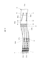
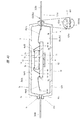
まず、図1〜図3を用いて本実施の形態の半導体装置が有する半導体チップ(センサチップ)の構造について説明する。図1は、本実施の形態の半導体装置が有するセンサチップの表面側を示す平面図、図2は、図1のA−A線に沿った断面図、図3は図1のB−B線に沿った断面図である。
<Structure of semiconductor chip (semiconductor sensor chip)>
First, the structure of a semiconductor chip (sensor chip) included in the semiconductor device of the present embodiment will be described with reference to FIGS. 1 is a plan view showing the surface side of a sensor chip included in the semiconductor device of the present embodiment, FIG. 2 is a cross-sectional view taken along the line AA in FIG. 1, and FIG. 3 is a line BB in FIG. FIG.
本実施の形態の半導体チップは、MEMS技術により形成されたセンサチップ1である。MEMS技術により形成したセンサチップ1は、可動部と、可動部の動きを電気信号に変換し、伝送する電気回路部(センサ回路)とを有し、例えば、加速度センサや角速度センサなど、種々の用途で利用可能である。本実施の形態では、センサチップの一例として、ピエゾ抵抗型の加速度センサを取り上げて説明する。センサチップ1は、例えば、フォトリソグラフィ技術やエッチング技術など半導体集積回路装置を製造する際に用いる微細加工技術を利用して形成するので、機械的に動作する可動部を有するセンサを小型化できるという利点がある。例えば、本実施の形態のセンサチップ1は、表面1aの平面形状が四角形から成り、各辺の長さは、例えば、1mm〜10mm程度である。
The semiconductor chip of this embodiment is a
本実施の形態のセンサチップ(半導体チップ)1は、表面(主面)1a、表面1aの反対側に位置する裏面(主面)1b、および表面1aと裏面1bの間に位置する側面1cを有している。詳しくは、センサチップ1は、本体部1k、および本体部1kの裏面1mに配置された蓋部1nを有し、蓋部1nの裏面がセンサチップ1の裏面1bとなっている。センサチップ1の本体部1kは、表面1aから裏面1mに向かって貫通するように形成された開口部1d、開口部1dの周囲に配置される支持体(枠体)1e、および開口部1d内に配置され、複数の梁(ビーム)1fを介して支持体1eに支持される錘部(可動部)1gを有している。
The sensor chip (semiconductor chip) 1 of the present embodiment has a front surface (main surface) 1a, a back surface (main surface) 1b located on the opposite side of the
センサチップ1の本体部1kは、例えばシリコンからなり、支持体1e、梁1f、および錘部1gは一体に形成されている。また、錘部1gを支持する複数の梁1fは、それぞれ可撓性を有し、センサチップ1に、検知対象である外力(例えば慣性力や重力)が印加され、この外力によって錘部1gが動くと、これに伴って複数の梁1fが撓む(弾性変形する)。また、複数の梁1fには、それぞれピエゾ抵抗素子が配置され、各ピエゾ抵抗素子は、センサチップ1に形成された配線(図示は省略)を介して、表面1aに形成された複数のパッド(電極パッド、ボンディングパッド)1hにそれぞれ電気的に接続されている。ピエゾ抵抗素子とは、応力によって抵抗値が変化する抵抗素子である。つまり、センサチップ1では、複数の梁1fが撓むことにより、梁1fに配置されたピエゾ抵抗素子の抵抗値が変化するので、これを利用して電気信号に変換し、パッド1hから電気信号を取り出す加速度センサである。このように、センサチップ1は、検知対象となる外力に応じて機械的に動作する可動部(錘部1g)と、可動部の動作を電気信号に変換する電気回路部(梁1f内のピエゾ抵抗素子)、および変換された電気信号を伝送する電気回路部(支持体1eに形成された図示しない配線やパッド1h)を備えている。
The
また、センサチップ1は、本体部1kの下面1m側に配置され、開口部1dを裏面1b側から被覆する蓋部1nを有している。この蓋部1nは、センサチップ1をダイボンディングした後で、接着材(ダイボンド材)が本体部に影響を及ぼすことを防止ないしは抑制する機能を有している。このため、蓋部1nは開口部1dを、センサチップ1の接着面(実装面)側である裏面1b側から本体部1kを覆うように配置されている。また、蓋部1nは、開口部1dと対向する領域に隙間1pを有している。センサチップ1では、隙間1pを形成することにより、錘部1gが動くためのスペースを確保している。ただし、センサチップの変形例として、接着面側に開口部1dが露出しない構造(例えば、本体部1kと蓋部1nが一体に形成された構造)とする場合もある。この場合は、蓋部1nを設けなくても良い。
The
ここで、センサチップ1は上記のように可動部の動作を電気信号として検出するので、センサとしての信頼性という観点から、感知対象である外力を印加しない状態において、錘部1gが所定の位置(基準位置)に配置され、梁1fに撓みが発生していないことが重要である。この観点から、センサチップ1を組み込む半導体装置(半導体パッケージ)においては、センサチップ1の本体部1kに印加される感知対象以外の外力を極力低減することが好ましい。このため、本実施の形態では、図2および図3に示すように、本体部1kにおいて、梁1fが配置される面である表面1a側には蓋部1nは配置していない。また、以下で説明するように、半導体装置の封止体内に空間を形成し、該空間内にセンサチップ1を配置する。
Here, since the
<半導体装置の概要構成>
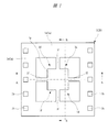
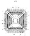
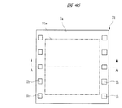
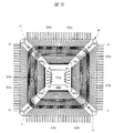
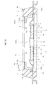
次に、図4〜図9を用いて、本実施の形態の半導体装置の構成例を説明する。図4は本実施の形態の半導体装置の上面側を示す平面図、図5は図4に示す半導体装置の下面側を示す平面図、図6は、図4のC−C線に沿った断面図、図7は、図4のD−D線に沿った断面図である。また、図8は、図4に示す半導体装置の封止体内部における平面構造を示す平面図、図9は図8のE部の拡大平面図である。なお、図8および図9は、半導体装置の内部構造を示す透視平面図であるため、図4に示す封止体9およびキャップ5を透過して内部構造を示す平面図としている。また、図6〜図8では、見易さのためセンサチップ1の詳細構造(図1〜図3に示す構造)は図示を省略している。
<Outline configuration of semiconductor device>
Next, a configuration example of the semiconductor device of this embodiment will be described with reference to FIGS. 4 is a plan view showing the upper surface side of the semiconductor device of the present embodiment, FIG. 5 is a plan view showing the lower surface side of the semiconductor device shown in FIG. 4, and FIG. 6 is a cross section taken along the line CC in FIG. 7 and 7 are cross-sectional views along the line DD in FIG. 8 is a plan view showing a planar structure inside the sealing body of the semiconductor device shown in FIG. 4, and FIG. 9 is an enlarged plan view of a portion E in FIG. 8 and 9 are perspective plan views showing the internal structure of the semiconductor device, and therefore are plan views showing the internal structure through the sealing
本実施の形態の半導体装置は、基材としてリードフレームを用い、そのチップ搭載部上に半導体チップが搭載されたリードフレームタイプの半導体パッケージであり、本実施の形態ではその一例として、図5に示すようなリードフレームタイプの半導体装置であるQFP(Quad Flat Package)10を取り上げて説明する。リードフレームタイプの半導体装置は、長年に亘って蓄積されたコスト低減技術を活用することができる。また、既に構築された製造設備等のインフラストラクチャーを活用することができるので、配線基板上に半導体チップを搭載する基板タイプの半導体装置と比較して製造コストを低減することができる。 The semiconductor device of the present embodiment is a lead frame type semiconductor package in which a lead frame is used as a base material and a semiconductor chip is mounted on the chip mounting portion. In the present embodiment, as an example, FIG. A QFP (Quad Flat Package) 10 which is a lead frame type semiconductor device as shown will be described. Lead frame type semiconductor devices can utilize cost reduction technology accumulated over many years. In addition, since an infrastructure such as a manufacturing facility that has already been constructed can be used, the manufacturing cost can be reduced compared to a substrate type semiconductor device in which a semiconductor chip is mounted on a wiring substrate.
まず、図4〜図9に示すQFP10の構成の概要について説明する。図6、図7に示すようにQFP10は、上面2a、上面2aの反対側の下面2b、および上面2aと下面2bの間に位置する側面2cを有するキャップ(第1部材、裏面側キャップ材)2を備えている。キャップ2は、金属材料から成る板状部材である。また、QFP10は、図1〜図3を用いて説明したセンサチップ1を備えている。センサチップ1は裏面1bを、キャップ2の上面2aと対向させた状態で、キャップ2の上面2a上に搭載されている。なお、図4〜図9に示す例では、QFP10はセンサチップ1を制御する半導体チップである制御チップ(コントローラチップ)6をQFP10内に内蔵しており、センサチップ1は制御チップ6上に搭載されている。また、QFP10は、センサチップ1(および、制御チップ6)の周囲に配置される複数のリード(端子)3を備えている。また、QFP10は、複数のリード3とセンサチップ1の複数のパッド1hを電気的に接続する複数のワイヤ4を有している。なお、QFP10は、前記の通り、センサチップ1の他、制御チップ6を備えており、図6および図9に示すようにセンサチップ1のパッド1hは、複数のワイヤ4aを介して制御チップ6の複数のパッド6dと電気的に接続され、制御チップ6のパッド6eは複数のワイヤ4bを介して複数のリード3と電気的に接続されている。また複数のパッド6dと複数のパッド6eのそれぞれは制御チップ6が備える複数の配線(図示は省略)を介して電気的に接続されている。つまり、QFP10では、センサチップ1の複数のパッド1hは、複数のワイヤ4a、4bおよび制御チップ6を介して複数のリード3と電気的に接続されている。また、QFP10は、図6および図7に示すように上面5a、上面5aの反対側の下面5b、および上面5aと下面5bの間に位置する側面5cを有するキャップ(第2部材、表面側キャップ材)5を備えている。キャップ5は、上面5aに向かって窪んだ形状を成し、下面5b側には、キャビティ部(空間形成部、凹部、窪み部、チップ収容部)5dおよびキャビティ部5dの周囲を取り囲むように配置されるフランジ部(接合部)5eを有している。キャップ5は、センサチップ1、複数のワイヤ4、および複数のリード3の一部(ワイヤ4がボンディングされるボンディング領域)が、キャビティ部5d内に位置するように、キャップ2の上面2a上に配置され、キャップ2とキャップ5の接合部(フランジ部5eの接着面5fとキャップ2の上面2aの間の領域)は、封着材7により封着されている。つまり、キャップ2とキャップ5を重ね合わせて接合することで、キャビティ部5d内の空間8を外部に対して密封された中空空間とし、空間8内にセンサチップ1、複数のワイヤ4、および複数のリード3の一部を配置している。また、QFP10は、キャップ2、5の接合部、および複数のリード3の他の一部(外部端子であるアウタリード部3bよりも内側のインナリード部3aであって、キャップ2、5よりも外側の領域)を封止する封止体(樹脂体)9を備えている。つまり、QFP10は、封止体9内に空間8を形成し、空間8内に半導体チップであるセンサチップ1を配置する半導体装置である。
First, an outline of the configuration of the
ここで、図6および図7に示すようにQFP10は、キャップ2の側面2cおよびキャップ5の側面5cは封止体9により覆われているが、キャップ2の下面2bおよびキャップ5の上面5aは、それぞれ面全体が封止体9から露出している。言い換えれば、図4に示すように、平面視において、キャップ5の上面5aの周縁部、および周縁部よりも内側の領域には封止体9が配置されていない。また、図5に示すように、平面視において、キャップ2の下面2bの周縁部、および周縁部よりも内側の領域には封止体9が配置されていない。詳細は後述するが、本実施の形態では、キャップ2の下面2b全体およびキャップ5の上面5a全体を露出させることにより、封止体9を形成する工程においてキャップ2、5に加わる圧力を低減し、特に、キャビティ部5dを有するキャップ5の変形を抑制することができる。このため、空間8の密封性を維持することができ、封止体9が空間8内に侵入することを防止ないしは抑制することができる。この結果、センサチップ1に封止体9が接触し、封止体9の応力などの影響により、センサチップ1およびQFP10の信頼性が低下することを抑制できる。なお、上面5aおよび下面2bの面全体が封止体9から露出する、とは、上面5aおよび下面2bの大部分が封止体9から露出しているという意味であり、例えば、封止体9を形成する工程において、封止体9と上面5aや下面2bの境界領域に樹脂バリなどが発生し、この樹脂バリが上面5aや下面2bを僅かに覆う態様を排除するものではない。また、同様に、上面5a(下面2b)の周縁部、および周縁部よりも内側の領域には封止体9が配置されていない、とは、例えば樹脂バリなどの僅かな樹脂を除き、封止体9が配置されていないという意味である。また、ここで言う樹脂バリとは、後述する封止工程において、熱硬化性樹脂(封止用樹脂)を構成する樹脂(レジン)が染み出したものであり、断面視または側面視では、その厚さがほとんど無いものを指す。
Here, as shown in FIGS. 6 and 7, in the
<半導体装置の詳細構成>
次に、QFP10が備える各部材の詳細構造について説明する。まず、キャップ2は、図8に示すように平面視において四辺形を成す平板であって、図6および図7に示すキャップ5のキャビティ部5dのような大きい窪み部(空間形成部)は有していない。キャップ2の一辺の長さは、例えば15mm〜20mm程度である。本実施の形態では、封止体9とキャップ2の界面において、封止体9の欠けが発生する事を抑制する観点から、キャップ2の四つの角部のそれぞれに面取り加工(R加工)を施している。ただし、キャップ2の平面形状は図8に示す態様に限定されず、例えば角部に面取り加工を施さない四角形の平面形状とすることもできる。また、キャップ2の厚さ(肉厚)は、QFP10の下面(実装面)側においてキャップ2の下面2bを露出させるため、例えばキャップ5よりも厚く形成されており、例えば0.1mm〜1mm程度である。キャップ2の強度を向上させる観点からは、キャップ2の厚さを厚くする程好ましいが、その場合、QFP10全体の厚さが厚くなる。また、本実施の形態によれば、キャップ2に加わる圧力を低減させることによりキャップ2の変形を抑制することができるので、キャップ2自体に要求される強度を低減することができる。したがって、キャップ2の下面が封止体9から露出する範囲であれば、キャップ2の厚さを薄くすることができる。例えば、キャップ5と同じ厚さ(肉厚)で形成することもできる。
<Detailed configuration of semiconductor device>
Next, the detailed structure of each member with which QFP10 is provided is demonstrated. First, the
また、QFP10では、キャップ2は、制御チップ6を搭載するチップ搭載部として機能する。言い換えれば、制御チップ6は、チップ搭載部としてのキャップ2の上面2a上に接着材(ダイボンド材)11を介して搭載される。制御チップ6は、表面6a、表面6aの反対側の裏面6b、および表面6aと裏面6bの間に位置する側面6cを有し、裏面6bを、キャップ2の上面2aと対向させた状態で搭載する、所謂、フェイスアップ実装方式により搭載されている。接着材11は、キャップ2の上面2aに制御チップ6を固定できるものであれば、特に限定されないが、本実施の形態では、例えば、エポキシ系の熱硬化性樹脂からなるペースト状の樹脂接着材を塗布して制御チップ6を接着した後、熱硬化させることにより固定する。また、制御チップ6の表面6a上には、接着材12を介してセンサチップ1が搭載される、センサチップ1は制御チップ6上にフェイスアップ実装方式により実装される。接着材12もセンサチップ1を制御チップ6上に固定するための部材であるが、センサチップ1の側面1c(図2参照)に接着材12の一部が付着して、接着材12に生じた応力がセンサチップ1の特性(検知特性)に悪影響を及ぼすことを抑制する観点から、接着材12はフィルム状の接着材とすることが好ましい。フィルム状の接着材は、ペースト状の接着材よりもセンサチップ1の側面1cに付着し難い点で好ましい。フィルム状の接着材は、例えば、DAF(Die Attach Film)と呼ばれ、半導体チップ上に別の半導体チップを積層する接着材として一般に使用されているものを使用することができる。
Further, in the
また、QFP10のように、キャップ2上にセンサチップ1を搭載する場合、キャップ2とセンサチップ1の線膨張係数の違いに起因して発生する応力の影響を低減する観点から、キャップ2は、センサチップ1と線膨張係数が近い材料で構成することが好ましい。このため、本実施の形態では、センサチップ1は例えばシリコンから成り、キャップ2はシリコンの線膨張係数と近い金属材料であるコバール(鉄にニッケル、コバルトを配合した合金)から成る。また、キャップ2と同様に、キャップ5もコバールから成る。詳しくはコバールから成る基材の表面(キャップ2の上面2aおよび下面2bと、キャップ5の上面5a、下面5bおよび側面5c)に例えばニッケル、あるいはニッケル・パラジウムからなるめっき膜を形成している。なお、ニッケル・パラジウムとは、ニッケル(Ni)とパラジウム(Pd)の合金からなるめっき膜の構成材料を指す。以下ではこのニッケルとパラジウムの合金をニッケル・パラジウムまたはNi/Pd、ニッケル・パラジウムから成るめっき膜をニッケル・パラジウム膜と記載する。このニッケル、あるいはニッケル・パラジウムからなるめっき膜(ニッケル膜、あるいはニッケル・パラジウム膜)は、キャップ2、5の酸化を防止する酸化防止膜として機能する。また、キャップ5の側面5cに形成しためっき膜(ニッケル膜、あるいはニッケル・パラジウム膜)は、封止体9とキャップ5の界面の密着性を向上させる密着性改善膜として機能する。また、センサチップ1への応力伝達を低減する観点から、QFP10のように、センサチップ1を直接キャップ2上に搭載せず、例えばシリコンから成る制御チップ6を介して搭載することが好ましい。これにより、センサチップ1に伝達される応力をさらに低減することができる。なお、本実施の形態におけるキャップ2の断面視における形状は、曲げ加工が施されていない、平板状である。すなわち、後述するキャップ5のように、曲げ加工が施されていないため、キャップ2の強度はキャップ5より低くても良い。そのため、封着材7を介して固定されるリード3と同じ材料(銅、あるいは銅合金)で構成してもよい。この場合も、コバールを使用した場合と同様に、基材の表面(キャップ2の上面2aおよび下面2bと、キャップ5の上面5a、下面5bおよび側面5c)に、例えばニッケル、あるいはニッケル・パラジウムからなるめっき膜を形成することが好ましい。
Further, when the
また、本実施の形態では、キャップ2の下面2bを露出させるので、キャップ2は空間8内で発生した熱をQFP10の外部に放熱する放熱部材(ヒートスプレッダ)として機能させることができる。この放熱経路としての観点からは、キャップ2をセラミック材料よりも熱伝導率が高い金属材料で構成することにより、セラミックパッケージと比較して放熱効率を向上させることができる。放熱部材として用いる場合、キャップ2の下面2b側に、例えば半田などの金属からなる接合材(図示は省略)を配置して、該接合材を介して実装基板(図示は省略)の端子(図示は省略)と接合することができる。この場合、実装基板への熱伝達をさらに効率化することができるので放熱効率がさらに向上する。
In this embodiment, since the
また、QFP10は、センサチップ1およびセンサチップ1を制御する制御チップ6を1つのパッケージ内に備えている。言い換えれば、QFP10は、パッケージ内に複数の半導体チップを混載し、複数の半導体チップを電気的に接続することにより、システムを構成している。このように、1つのパッケージ内にセンサチップ1と制御チップ6とを混載することにより、センサチップ1と制御チップ6とを別々のパッケージとする場合と比較して実装面積を小さくすることができる。
Further, the
次に、センサチップ1および制御チップ6の周囲には複数のリード(端子)3が配置される。複数のリード3は、QFP10の外部端子であって、封止体9の内側(空間8内も含む)に配置されるインナリード部3aと、封止体9の外側に配置されるアウタリード部3bは、一体に形成されている。また、複数のリード3は例えば銅、あるいは銅合金からなり、表面(上面、下面および側面(上面と下面との間に位置する面)に例えばニッケル、あるいはニッケル・パラジウムからなるめっき膜(金属膜)が形成されている。なお、このめっき膜は、必ずしも複数のリード3のそれぞれの全面に形成されていなくてもよいが、全面に形成しない場合は、封止体9を形成した後に、この封止体9から露出するアウタリード部3bの表面(上面、下面および側面)に、鉛の半田材、あるいは鉛を実質的に含有しない半田材(鉛フリー半田)からなるめっき膜(外装めっき膜)を形成する。図6に示すアウタリード部3bは、封止体9の側面から突出するように配置され、封止体9の外側において曲げ加工が施されている。例えば、図6ではガルウィング状に形成された例を示している。一方、図6に示すインナリード部3aは、アウタリード部3bとの境界から空間8内に向かって延び、その先端部は、空間8内に配置されている。また、空間8内にインナリード部3aを配置するため、インナリード部3aの先端部(図13に示すボンディング領域3c)は、キャップ2の上面2a上に配置されている。このように、空間8内にインナリード部3aの一部を配置することで、制御チップとリード3を接続するワイヤ4bの接合部を空間8内(キャビティ部5d内)に配置することができる。つまり、インナリード部3aの先端部周辺は、ワイヤ4bを接合するボンディング領域となっており、このボンディング領域をキャビティ部5dの内側に配置することで、キャップ5によりワイヤ4bを覆うことができる。また、前記したようにキャップ2はコバール、銅、あるいは銅合金などの金属材料(導電材料)からなる。したがって、キャップ2上に配置した複数のリード3とキャップ2を絶縁しなければ、複数のリード3間で短絡が生じる。このため、QFP10では、キャップ2の上面2aとリード3の下面の間に絶縁性の接着材13を配置し、接着材13を介してリード3をキャップ2に接着固定している。
Next, a plurality of leads (terminals) 3 are arranged around the
また、図8に示すように平面視において、QFP10の有する四辺に沿ってそれぞれ複数のリード3が配置されている。半導体チップを基準に考えると、センサチップ1および制御チップ6はそれぞれ四辺形の平面形状を成し、平面視において四辺のそれぞれと対向する位置に複数のリード3が配置されている。図8および図9に示す例では、制御チップ6の有する四辺のうち、互いに対向する二辺に沿って複数のパッド6e(図9参照)が配置され、複数のパッド6eと対向する位置に配置される複数のリード3にワイヤ4bが接続されている。一方、パッド6eが配置されていない辺と対向する複数のリード3にはワイヤ4は接続されていない。このように、リード3の数が半導体チップの端子(パッド)数よりも多い場合、一部のリード3には、ワイヤ4を接続しない構成とすることができる。また、図8および図9に示すQFP10は、センサチップ1の複数のパッド1h(図9参照)と複数のリード3は、直接ワイヤ4を介して接続されていない。つまり、センサチップ1の複数のパッド1hのうちワイヤ4が接続されるパッド1hは、全てワイヤ4aを介して制御チップ6のパッド6d(図9参照)と接続される。また、複数のリード3のうち、ワイヤ4が接続されるリード3は、全てワイヤ4bを介して制御チップ6のパッド6eと接続される。このようにセンサチップ1のパッド1hを、制御チップ6を介してリード3と接続することにより、パッド1hに接続されるワイヤ4aのワイヤ長を短くすることができる。例えば図6や図8に示すように、ワイヤ4aのワイヤ長は、ワイヤ4bの長さよりも短い。図6に示すように、複数のワイヤ4を空間8内に配置する場合、QFP10に印加された振動などの外力により、ワイヤ4が振動する場合があり、特に、センサチップ1に接続されるワイヤ4aが大きく振動すると、センサチップ1の特性(検知特性)が低下するおそれがある。QFP10に加わる外力を一定とすると、ワイヤ4の長さを短くすることにより振動の程度が小さくなる。したがって、センサチップ1の特性(検知特性)低下を抑制する観点から、センサチップ1の複数のパッド1hのうちワイヤ4が接続されるパッド1hは、全てワイヤ4aを介して制御チップ6のパッド6dと接続することが好ましい。ただし、ワイヤリングのレイアウトは、図8および図9に示す態様には限定されず、リード3と接続する半導体チップの端子(パッド)数やレイアウトに応じて種々の変形例を適用することができる。
Further, as shown in FIG. 8, a plurality of
次に、制御チップ6およびセンサチップ1上には、キャップ(第2部材、表面側キャップ材)5が配置される。図6および図7に示すようにキャップ5は、上面5a、上面5aの反対側の下面5b、および上面5aと下面5bの間に位置する側面5cを有している。キャップ5は、コバールから成り、表面(上面5a、下面5bおよび側面5c)にニッケルからなるめっき膜が形成されている。また、キャップ5の下面5b側には、キャップ5の略中央部に配置されるキャビティ部5d、およびキャビティ部5dの周囲を取り囲むフランジ部(接合部)5eが配置されている。QFP10では、キャップ5のフランジ部5eとキャップ2の上面2aの周縁部を封着材7(および接着材13)を介して接合し、これによりセンサチップ1、制御チップ6、複数のワイヤ4および複数のリード3それぞれの一部(ボンディング領域)を空間8内に密封している。キャビティ部5dの深さは、半導体チップ(センサチップ1および制御チップ6)の厚さよりも深いが、QFP10の厚さに影響を与えるのでパッケージの薄型化に対応するためには出来る限り浅くすることが好ましい。例えば、本実施の形態では1mm〜3mm程度である。また、キャビティ部5dの平面サイズは、センサチップ1および制御チップ6の平面サイズよりも大きく、例えば、平面視において四辺形を成すキャビティ部5dの一辺の長さは、例えば13mm〜18mm程度である。
Next, a cap (second member, surface-side cap material) 5 is disposed on the
ここで、封着材7は、キャップ2とキャップ5の接合部に配置される部材なので、空間8内の密封性を向上させる観点から、高い封着特性(隣り合うリード3の間に埋め込む特性、塗布してから接着固定するまでの間に形状を保つ特性、および接着界面の密着性)が要求される。本実施の形態では、高い封着特性が要求される封着材7は、以下の材料が好ましい。すなわち、隣り合うリード3の間に生じる隙間を低減する観点から、フィルム状(テープ状)の接着材(例えば、接着材12のような接着材)のように固形状態で接着する材料よりも、硬化させる前にはペースト状の性状を有する材料が好ましい。また、封着材7を塗布してから硬化させるまでの間は、塗布形状を保つ必要があるので、ある程度粘度が高い方が好ましい。例えば、水のような粘度の封着材では、塗布形状を保つことができない。一方、粘度が高すぎると、隣り合うリード3の間に隙間が生じてしまう場合がある。そこで、キャップ2およびリード3上に塗布した後、硬化させてキャップ2、5の接合部を固定するまでの間は、塗布形状を保つことができる範囲で、粘度を低くすることが好ましい。例えば、本実施の形態では、接着材11および封着材7は、エポキシ系の熱硬化性樹脂にフィラ(粒子)を混合した接着材を用いているが、封着材7の硬化前の粘度は、接着材11の硬化前の粘度よりも低い。このような粘度調整は、接着材に添加するフィラの形状、粒径の他、粘度調整用のバインダ材などの添加材料の配合割合を調整することにより行うことができる。また、封着材7を硬化させた後は、キャップ2、5およびリード3との接着界面が密着して固定されていることが要求される。本実施の形態では、キャップ2の上面2a、キャップ5のフランジ部5eの接着面5f、およびリード3の表面のそれぞれに同じ金属材料(例えばニッケル、あるいはニッケル・パラジウム)からなるめっき膜を形成しているので、接合部に配置される各部材との密着性を容易に向上させることができる。なお、複数のリード3とキャップ2の上面2aを接着固定する接着材13も、接合部に配置される部材である。したがって、接着材13も封着材7と同じ材料を用いることができる。ただし、封着材7をペースト状の熱硬化性樹脂とすれば、例えば、接着材13にフィルム状の接着材を用いても隣り合うリード3の間の隙間には封着材7が埋め込まれる。このため、本実施の形態では、接着材13は、取り扱いが容易なフィルム状の接着材(例えば接着材12と同様に、フィルム基材の表面に)としている。
Here, since the sealing
次に、キャップ2、5の接合部は、封止体9により覆われている。この封止体9は、所謂、プラスチックパッケージと呼ばれる樹脂封止型の半導体装置において一般に用いられる樹脂であって、例えば、本実施の形態では、トランスファモールド方式(詳細は後述する)により形成されている。図6に示すように、QFP10は、半導体チップ(センサチップ1および制御チップ6)およびこれに接続される複数のワイヤ4のそれぞれが、キャップ2、5を重ね合わせることにより形成される空間8内に配置されているので、封止体9を形成しない態様も変形例として考えられる。しかし、封止体9を形成しない場合、キャップ2、5の接合部が露出するため、例えば衝撃や熱影響などの外力により接合部が破壊され易くなる。また、接合部の破壊を抑制するため、封着材7および接着材13の強度を上げようとすれば、空間8の密封性が損なわれる懸念がある。また、製造工程が煩雑になる。したがって、図6に示すように、キャップ2、5の接合部の外側を封止体9で覆い、接合部を保護することが好ましい。これにより、封着材7および接着材13は、前記した封着特性を考慮して最適な材料を選択することができる。また、接合部の強度は封止体9により補強されるので、封止体9を形成しない場合と比較して、接合部の破壊を抑制することができる。
Next, the joint part of the
また、図8に示すように、平面視において封止体9は四つの辺(角部の面取り加工部以外の主辺)を備える四辺形を成し、各辺の交点となる角部には、それぞれ吊りリード14が配置されている。この吊りリード14は、後述するQFP10の製造工程において、封止体9が形成されてからQFP10が個片化されるまでの各工程中に、封止体9内の領域を基材であるリードフレームにより支持するための支持部材である。このため、複数の吊りリード14は、複数のリード3と同じ材料(例えば銅あるいは銅合金)で構成される。一方、キャップ2、5は、本実施の形態では、前記したように例えばコバールからなり、吊りリード14とは別体として形成されているが、上述のように、キャップ2については、リード3と同じ材料(例えば銅あるいは銅合金)であってもよい。
Further, as shown in FIG. 8, the sealing
<半導体装置の製造工程>
次に図5〜図9に示すQFP10の製造工程について説明する。QFP10は、図10に示す組み立てフローに沿って製造される。図10は、本実施の形態の半導体装置の組み立てフローを示す説明図である。各工程の詳細については、図11〜図31を用いて、以下に説明する。
<Manufacturing process of semiconductor device>
Next, a manufacturing process of the
1.リードフレーム準備工程;
図11は、図10に示すリードフレーム準備工程で準備するリードフレームの全体構造を示す平面図、図12は、図11に示す複数の製品形成領域のうち、1つの製品形成領域周辺の拡大平面図である。また、図13は図12のF−F線に沿った拡大断面図である。
1. Lead frame preparation process;
FIG. 11 is a plan view showing the overall structure of the lead frame prepared in the lead frame preparation step shown in FIG. 10, and FIG. 12 is an enlarged plan view around one product formation region among the plurality of product formation regions shown in FIG. FIG. FIG. 13 is an enlarged sectional view taken along line FF in FIG.
まず、図10に示すリードフレーム準備工程として、図11に示すようなリードフレーム20を準備する。本実施の形態で使用するリードフレーム20は、枠部(枠体)20bの内側に複数の製品形成領域20aを備えている。複数の製品形成領域20aは、行列状に配置されている。また、隣り合う製品形成領域20aの間にも枠部20bが配置されている。隣り合う製品形成領域20aの間には、後述する封止工程において、封止用樹脂を各製品形成領域20a内に配置されるキャビティに向かって供給するための供給経路であるランナ部が配置される領域であるランナ領域20cが列方向に沿って配置されている。
First, as a lead frame preparation step shown in FIG. 10, a
各製品形成領域20aには、図11の部分拡大図である図12に示すように、キャップ2が製品形成領域20aの中央部に配置されている。一般に、リードフレーム型の半導体装置の製造工程においては、製品形成領域の中央部に、半導体チップを搭載するためのチップ搭載部であるダイパッド(タブ)を配置し、吊りリードを介してリードフレームの枠部と接続するが、本実施の形態では、キャップ2がチップ搭載部を兼ねるので、リードフレームと一体に形成されたダイパッドは形成されていない。本実施の形態では、キャップ2はリードフレーム20とは、異なる材料により形成される。例えばリードフレーム20は、金属から成り、本実施の形態では、例えば、銅(Cu)、あるいは銅合金から成る。詳しくは、図13に示すように銅(Cu)から成る基材21の表面に、例えばニッケル(Ni)、あるいはニッケル・パラジウム(Ni/Pd)からなるめっき膜(金属膜)22が形成されている。一方、キャップ2は、例えばコバールからなる基材23の表面に、例えばニッケル(Ni)、あるいはニッケル・パラジウム(Ni/Pd)からなるめっき膜(金属膜)22が形成されている。このため、キャップ2は、リードフレーム20とは別体として形成され、接着材13を介して複数のリード3と接着固定されている。この時、リード3およびキャップ2のそれぞれの接着材13との接着界面は、それぞれニッケル、あるいはニッケル・パラジウムからなるめっき膜22となっているため、接着材13との密着性を向上させることができる。なお、本工程では、図12に示すように複数のリード3とキャップ2が接着固定された状態のリードフレーム20を準備する。したがって、以降の説明において、特にキャップ2を区別して説明する場合を除き、リードフレーム20には、複数のリード3に接着固定されたキャップ2が含まれる。
In each
また、図12に示すように、キャップ2の周囲には、複数のリード3が配置される。このリード3は、図6に示すように完成時に封止体9により封止されるインナリード部3aと、封止体9から露出するアウタリード部3bから成る。また、図13に示すようにインナリード部3aは、リード3の内側の端部から順に配置されるボンディング領域3c、封着領域3dおよび封止領域3eを有している。また、アウタリード部3bは、インナリード部3aとの境界から順に配置されるダム領域3fおよび最外領域3gを有している。ボンディング領域3cは、リード3の内側の端部に配置され、ワイヤボンディング工程(図10参照)でワイヤ4(図6参照)を接合する領域である。また、封着領域3dは、ボンディング領域3cとアウタリード部3bの間に配置され、キャップボンディング工程(図10参照)で、キャップ5(図6参照)のフランジ部5e(図6参照)の間で封着材7(図6参照)により封止される領域である。また、封止領域3eは、封着領域3dとアウタリード部3bの間に配置され、封止工程(図10参照)で、封止体9(図6参照)により封止される領域である。また、ダム領域3fは、封止領域3eと最外領域3gの間に配置され、封止工程(図10参照)で、封止用樹脂を成形金型内に供給する際にダムとなるダム部24(図12参照)が接続される領域である。また、最外領域3gは、リード3の外側の端部に配置され、リード成形工程(図10参照)で例えば図6に示すようなガルウィング状に曲げ加工が施される領域である。
Further, as shown in FIG. 12, a plurality of
また、図12に示す複数のリード3のダム領域3f(図13参照)の間には、複数のリード3と交差(直交)するように延びるダム部(ダムバー、タイバー)24が配置され、複数のリード3は、ダム部24を介してリードフレーム20と一体に形成されている。ダム部24は、キャップ2の周囲を取り囲むように配置されている。後述する封止工程(図10参照)では、このダム部24で囲まれた領域の内側に封止用樹脂を供給し図6に示す封止体9を形成する。また、ダム部24が形成する四辺形の角部には、それぞれ吊りリード14が配置されている。言い換えれば、隣り合う吊りリード14の間には、それぞれ複数のリード3が配置されている。吊りリード14は、図10に示すリード成形工程で複数のリード3の最外領域3g(図13参照)を切断した後、個片化工程で切断されるまでの間、製品形成領域20a内の各部材をリードフレーム20に支持される部材である。このため、リードフレーム20と一体に形成されている。
Further, between the
図11〜図13に示すリードフレーム20は、例えば、以下のように形成することができる。まず、銅(Cu)からなる薄板を用意してエッチング加工により、例えば、図12に示すパターンで複数のリード3、複数の吊りリード14、およびダム部24を形成する。また、図11に示す製品形成領域20aの数に対応させて、複数のキャップ2を準備して、上面2aの周縁部に接着材13を配置する。そして、キャップ2の上面2aの接着材13を配置した領域と、複数のリード3の先端領域(図13に示すボンディング領域3cおよび封着領域3d)が重なるように位置合わせを行い、キャップ2とリード3を接着する。次に、例えばキャップ2が接着されたリードフレーム20を加熱することで接着材13を硬化させて、キャップ2と複数のリード3を固定する。この時、図6に示す空間8の密封性を向上させるためには、リード3の下面とキャップ2の上面2aの間に隙間が生じないように接着材13を配置することが重要である。一方、ペースト状の接着材の場合、接着材13の量が多すぎると、接着材13の一部が、ボンディング領域3c(図13参照)の上面側に廻り込んで、ワイヤボンディング工程(図10参照)の際にボンディング不良が発生する原因となる。このため、接着材13は、フィルム状の接着材(詳しくは、基材となる樹脂フィルムの上面および下面に接着層となる例えば熱硬化性樹脂層を配置した接着材)を用いることが好ましい。
The
なお、上記では、図11に示す製品形成領域20aの数に対応させた複数のキャップ2をそれぞれ準備して、それぞれ複数のリード3と位置合わせを行う態様について説明したが、種々の変形例を適用することができる。例えば、複数のキャップ2を図示しない吊りリード(キャップ連結用の吊りリード)を介して連結することで一体化し、キャップ2をリード3と接着固定した後で、該吊りリードを切断する態様とすることができる。この場合、複数の製品形成領域20aにそれぞれ配置されるキャップ2とリード3の位置合わせを一括して行うことができる。この場合、複数のキャップ2を連結する図示しない吊りリードを切断するスペースが必要となるため、リードフレーム20と一体に形成された吊りリード14は、キャップ2とは離間して配置することが好ましい。これにより、吊りリード14とキャップ2の間のスペースにおいて、複数のキャップ2を連結する図示しない吊りリードを切断することができる。また、連結されない複数のキャップ2をそれぞれリード3に接着固定する場合、図12に対する変形例として複数の吊りリード14をリード3と同様にキャップ2の上面2a側に接着固定することもできる。
In the above description, a description has been given of a mode in which a plurality of
2.半導体チップ準備工程;
次に、図10に示す半導体チップ準備工程として、図6に示す複数の半導体チップ(センサチップ1および制御チップ6)を準備する。本工程では、複数のチップ領域を有し、例えば、シリコンからなる半導体ウエハ(図示は省略)を準備する。その後、半導体ウエハのダイシングラインに沿って、ダイシングブレードを走らせて(図示は省略)半導体ウエハを分割し、複数種類の半導体チップをそれぞれ複数個取得する。詳しくは、複数のチップ領域のそれぞれに図1〜図3に示すセンサチップ1が備えるセンサ(可動部)および可動部と電気的に接続されるセンサ回路をMEMS技術により形成した半導体ウエハを準備する。また複数のチップ領域のそれぞれに図6〜図8に示す制御チップ6がそなえる制御回路を形成した半導体ウエハを準備する。そして各半導体ウエハをそれぞれ個片化して、複数のセンサチップ1および複数の制御チップ6を取得する。なお、本実施の形態では、図6に示すセンサチップ1は、例えばDAFと呼ばれるフィルム状の接着材を介して制御チップ6の表面6a上に搭載するので、本工程で取得する複数のセンサチップ1の裏面1bには、それぞれ接着材12が貼り付けられている。
2. Semiconductor chip preparation process;
Next, as a semiconductor chip preparation step shown in FIG. 10, a plurality of semiconductor chips (
3.半導体チップ搭載工程;
図14は、図12に示すキャップ上に接着材を介して半導体チップ(制御チップ)を搭載した状態を示す拡大平面図、図15は図14のG−G線に沿った拡大断面図である。また、図16は、図14に示す制御チップ上に接着材を介して半導体チップ(センサチップ)を搭載した状態を示す拡大平面図、図17は図16のG−G線に沿った拡大断面図である。なお、図14および図16では、見易さのため、図12に示すキャップ2の周辺をさらに拡大してしめしている。
3. Semiconductor chip mounting process;
14 is an enlarged plan view showing a state in which a semiconductor chip (control chip) is mounted on the cap shown in FIG. 12 via an adhesive, and FIG. 15 is an enlarged cross-sectional view taken along line GG in FIG. . 16 is an enlarged plan view showing a state in which a semiconductor chip (sensor chip) is mounted on the control chip shown in FIG. 14 via an adhesive, and FIG. 17 is an enlarged cross section taken along line GG in FIG. FIG. 14 and 16, the periphery of the
次に、図10に示す半導体チップ搭載工程として、図14〜図17に示すように制御チップ6およびセンサチップ1を順次、キャップ2の上面2a上に搭載する。本工程では、図14および図15に示すように、下層に配置される半導体チップである制御チップ6を先にキャップ2の上面2a上に接着材11を介して搭載する。本実施の形態では、図14に示すように、制御チップ6は表面6aの有する四辺のうち、互いに対向する二辺に沿ってそれぞれ複数のパッド6d、6eが形成されている。本工程では制御チップ6の、パッド6eが配置された二辺が、キャップ2上に接着固定されたリード群(複数のリード3)とそれぞれ対向するようにキャップ2の中央部にキャップ2の各辺に沿って配置する。また、図15に示すように、制御チップ6の裏面6bをキャップ2の上面2aと対向させた状態で搭載する、所謂フェイスアップ実装方式で搭載する。
Next, as a semiconductor chip mounting step shown in FIG. 10, the
また、本実施の形態では、例えば、エポキシ系の熱硬化性樹脂である接着材11を介して制御チップ6を搭載するが、接着材11は、硬化(熱硬化)させる前には流動性を有するペースト材である。このようにペースト材を接着材11として用いる場合には、まず、キャップ2の上面2aのチップ搭載領域上に、ペースト状の接着材11を塗布する。次に、例えば図15に示す押圧治具30を制御チップ6の表面6a側に押し当てて、制御チップ6の裏面6bをキャップ2の上面2aに向かって押し付けることで、接着材11を制御チップ6の裏面6b全体に濡れ広がらせて接着する。そして、接着後に、接着材11を硬化させる(例えば熱処理を施す)と、図14および図15に示すように、制御チップ6は接着材11を介してチップ搭載領域2d上に固定される。なお、変形例として、接着材11をフィルム状の接着材とすることもできる。さらには、キャップ2への放熱性の向上を考慮すれば、熱伝導率の高い導電性粒子を含有する接着材を用いてもよい。ただし、金属(例えばニッケル、あるいはニッケル・パラジウム)から成るキャップ2の上面2aとの接着強度を向上させることができる点で、ペースト状の接着材の方が好ましい。このようにペースト状の接着材11を用いる場合には、接着材11を制御チップ6の裏面6b全体に濡れ広がらせるため、図14および図15に示すように、接着材11の外縁部は、制御チップ6の外縁部よりも外側まで広がる。ここで、QFP10(図6参照)の信頼性低下を抑制する観点からは、接着材11の一部が制御チップ6の表面6a側まで濡れ上がり、パッド6d、6dを覆う、あるいはセンサチップ1(図6参照)にまで達することを抑制する必要がある。したがって、接着材11の配置量(塗布量)は、制御チップ6の裏面6b全体に濡れ広がる範囲内で少なくする事が好ましい。また、接着材11の粘度を有る程度高くすることで、表面6a側への濡れ上がりを抑制することができる。このため、接着材11の硬化前の粘度は、図6に示す封着材7の硬化前の粘度よりも高くなっている。
In the present embodiment, for example, the
次に、図16および図17に示すように制御チップ6の表面6a上に、接着材12を介してセンサチップ1を搭載する。本工程では、センサチップ1の裏面1b側(接着材12が貼着された面)を制御チップ6の表面6aと対向させた状態で、制御チップ6の表面6a上に配置する。センサチップ1は、例えば図17に示す押圧治具31を制御チップ6の表面6a側に押し当てて、センサチップ1の裏面1bを制御チップ6の表面6a上に押し付けて接着させることにより搭載する。ここで、センサチップ1の裏面1bにはフィルム状の接着材12が予め貼り付けられているので、制御チップ6を搭載する場合よりも弱い押し付け力で、センサチップ1を搭載することができる。このため、本工程によるセンサチップ1の損傷を抑制できる。また、フィルム状の接着材12を用いれば、図17に示すように接着材12はセンサチップ1の裏面1bの外縁よりも外側に張り出ないので、センサチップ1の側面1cに接着材12の一部が付着する、あるいは制御チップ6のボンディングパッド6bに接着材の一部が付着する(汚染する)ことを抑制できる。次に、接着材12の接着層を硬化させてセンサチップ1を制御チップ6の表面6a上に固定する。
Next, as shown in FIGS. 16 and 17, the
4.ワイヤボンディング工程;
図18は、図16に示す半導体チップと複数のリードを、ワイヤを介して電気的に接続した状態を示す平面図、図19は、図18のG−G線に沿った拡大断面図である。
4). Wire bonding process;
18 is a plan view showing a state in which the semiconductor chip shown in FIG. 16 and a plurality of leads are electrically connected via wires, and FIG. 19 is an enlarged cross-sectional view taken along the line GG in FIG. .
次に、図10に示すワイヤボンディング工程として、図18および図19に示すように、半導体チップの複数のパッドと複数のリード3とを、複数のワイヤ4を介して、それぞれ電気的に接続する。本工程では、センサチップ1の複数のパッド1hと制御チップ6の複数のパッド6dを複数のワイヤ4aを介してそれぞれ電気的に接続する。また、制御チップ6の複数のパッド6eと複数のリード3を複数のワイヤ4bを介してそれぞれ電気的に接続する。
Next, as a wire bonding step shown in FIG. 10, as shown in FIGS. 18 and 19, a plurality of pads of the semiconductor chip and a plurality of
詳しくは、例えば、図19に示すようにワイヤボンディング時の加熱源であるヒートステージ32を準備し、リードフレーム20をヒートステージ32上に配置し、キャップ2を介して制御チップ6およびセンサチップ1を加熱する。一方、キャピラリ33の先端部から突出したワイヤ34の一端部を放電させることでボール部を形成し、このボール部を第1ボンド側となるパッド1hまたはパッド6eに接合する。ワイヤ34の接合方式は、超音波および熱圧着を併用して接合する、所謂、ネイルヘッドボンディング方式で接合する。第1ボンド側を接合した後は、キャピラリ33から徐々にワイヤ34を繰り出しながら、キャピラリ33を移動させてワイヤ4のループ形状を形成する。そして、第2ボンド側となるパッド6dまたはリード3のボンディング領域3c(図13参照)にワイヤ34を接合した後にワイヤ34を切断し、図19に示すようなループ形状を備えたワイヤ4が形成される。ワイヤ4a、4bの接続順序は特に限定されない。また、本実施の形態では相対的に上方に位置するパッド1h、6eを第1ボンド側とする、所謂、正ボンディング方式によりワイヤ4を形成しているが、変形例として、パッド1h、6eを第2ボンド側とする、所謂、逆ボンディング方式を適用することもできる。なお、正ボンディング方式によりワイヤ4(4a)を形成する場合は、第2ボンド側となるパッド6d上に、例えばワイヤの一部から成るバンプ(図示しない)を予め形成しておき、このバンプにワイヤ4(4a)の一部を接続する。一方、逆ボンディング方式を適用する場合は、パッド1e、6d上に例えばワイヤの一部から成るバンプ(図示しない)をそれぞれ形成しておき、このバンプにワイヤ4(4a、4b)の一部を接続する。
Specifically, for example, as shown in FIG. 19, a
5.キャップボンディング工程;
図20は、図18に示すキャップ上に別のキャップを重ね合わせて接着固定した状態を示す拡大平面図、図21は、図20のG−G線に沿った拡大断面図、図22は図20のH−H線に沿った拡大断面図である。また、図23は、図18に示すキャップおよび複数のリード上に封着材を塗布した状態を示す拡大平面図、図24は、図20のH−H線に沿った断面に対応する図23の拡大断面図である。
5. Cap bonding process;
20 is an enlarged plan view showing a state in which another cap is overlapped and fixed on the cap shown in FIG. 18, FIG. 21 is an enlarged cross-sectional view taken along line GG in FIG. 20, and FIG. It is an expanded sectional view along the 20 HH line. 23 is an enlarged plan view showing a state in which a sealing material is applied on the cap and the plurality of leads shown in FIG. 18, and FIG. 24 is a cross-sectional view taken along line HH in FIG. FIG.
次に、図10に示すキャップボンディング工程として、図21に示すように、キャップ(第2部材、表面側キャップ材)5を準備して、キャップ2の上面2a上に配置し、キャップ5のキャビティ部5dの外側に設けられたフランジ部5eの接着面(下面)5fとキャップ2の上面2aとを封着材7を介して接着固定(搭載)する。キャップ5の搭載方法は、例えば以下のように行う。
Next, as a cap bonding step shown in FIG. 10, as shown in FIG. 21, a cap (second member, front-side cap material) 5 is prepared and placed on the
まず、図23および図24に示すように、キャップ2の上面2aの周縁部にペースト状の封着材7を塗布する。次に、封着材7を塗布した領域と図22および図23に示すキャップ5のフランジ部5eの接着面5fが対向するように、キャップ2上にキャップ5を配置する。そして、例えば図示しない押圧治具によりキャップ5を上面5a側からキャップ2に向かって押し付けることで、フランジ部5eの接着面5fをキャップ2の上面2a側に押し込むと、図22および図23に示すように封着材7は隣り合うリード3の間の隙間に埋め込まれるように濡れ広がり、フランジ部5eの接着面5fとキャップ2の上面2aは、封着材7を介して接着される。次に、ペースト状の封着材7を加熱して、硬化させると、フランジ部5eの接着面5fとキャップ2の上面2aが固定され、キャップ5はキャップ2上に搭載される。本実施の形態では、封着材7には、例えばエポキシ系の熱硬化性樹脂が含まれているので、封着材7を加熱することでこれを硬化させることができる。
First, as shown in FIGS. 23 and 24, a paste-
図21に示すようにキャップ5は、上面5a、上面5aの反対側の下面5b、および上面5aと下面5bの間に位置する側面5cを有するキャップ5を備えている。キャップ5は、上面5aに向かって窪んだ形状を成し、下面5b側には、キャビティ部(空間形成部、凹部、窪み部、チップ収容部)5dおよびキャビティ部5dの周囲を取り囲むように配置されるフランジ部(接合部)5eを有している。キャップ5は、例えばコバールからなる平板にプレス加工を施すことにより、キャビティ部5dおよびフランジ部5eを形成することで得られる。なお、キャップ5の形成方法としては、これに限らず、一つの厚い平板の一部(中央部)を除去する(くり貫く)ことによって、キャビティ部5dおよびフランジ部5e(平板の底面から突出する部分)を形成してもよい。
As shown in FIG. 21, the
また、キャビティ部5dの平面サイズは、センサチップ1、制御チップ6、複数のワイヤ4、および複数のリード3の一部(図13に示すボンディング領域3c)を内部に収める(収容する)ことができるサイズになっている。このため、本工程では、センサチップ1、制御チップ6、複数のワイヤ4、および複数のリード3の一部(ボンディング領域3c)は、キャップ5に覆われる。言い換えれば、本工程では、キャップ5は、センサチップ1、制御チップ6、複数のワイヤ4、および複数のリード3の一部(ボンディング領域3c)を覆うように、キャップ2の上面2a上に接着固定される。また、複数のリード3は、インナリード部3aとアウタリード部3bが一体に形成されるため、複数のリード3のそれぞれは、キャップ5のキャビティ部5dの内側からキャビティ部5dの外側に向かって延びるように配置される。そして、キャップ2、5を接着固定した後は、センサチップ1、制御チップ6、複数のワイヤ4、および複数のリード3の一部(ボンディング領域3c)は、これらの部材の周囲を取り囲むように配置された接合部(封着領域)により密封された空間8内に配置される。
The
また、前記したように、ペースト状の封着材7は、塗布された形状(例えば図24に示す形状)を保持できる程度の粘度を有している。このため、封着材7を塗布した後、キャップ5を接着するまでの間に封着材7が塗布領域の周囲に広がってしまうことを抑制できる。また、ペースト状の封着材7の粘度は、図15に示すペースト状の接着材11の粘度よりも低い。このため、図23に示すように、隣り合うリード3の間に隙間が生じないように封着材7を埋め込むことができる。言い換えると、封着材7を塗布する領域には複数のリード3が配置されているためキャップ2の上面2aよりも粗い凹凸面となっている。このため、封着材7を塗布した段階では、図24に示すように封着材7とキャップ2の上面の間には隙間が生じている場合がある。しかし、キャップ5を押し付けてペースト状の封着材7を押し広げる事で、この隙間に封着材7を埋め込むことができる。特に、図15に示すペースト状の接着材11よりも粘度が低い封着材7を用いれば、その埋め込み特性が向上するので、封着材7が埋め込まれていない隙間の発生を効果的に抑制することができる。
Further, as described above, the paste-
ところで、図23と図24では、封着材を塗布する方法の一例について説明した。しかし、図21および図22に示すようにキャップ5の一部(ここでは、フランジ部5e)とキャップ2の上面2aが接着された段階で、封着材7がセンサチップ1、制御チップ6、複数のワイヤ4、および複数のリード3のボンディング領域の周囲を取り囲み、かつ、封着領域(接合部)のリード3間の隙間の発生を抑制することができれば、塗布方法は特に限定されない。例えば、図23および図24では、ペースト状の封着材7をキャップ2の上面2aの周縁部に沿って帯状に配置する態様について示した。しかし、変形例として、キャップ2の上面2aの周縁部(図23に示す封着材7を配置した領域)に沿って複数箇所にペースト状の封着材7を配置する、所謂、多点塗布方式とすることもできる。多点塗布方式の場合でも、キャップ5を押し付けてペースト状の封着材7を押し広げれば、リード3間の隙間に封着材7を埋め込むことができる。また例えば、図23および図24では、キャップ2上にペースト状の封着材7を塗布する方式について説明した。しかし、封着材7を塗布する部材はキャップ2に限定されず、例えば、キャップ5のフランジ部5eの接着面5fに塗布することができる。また例えば、キャップ2の上面2aの周縁部およびキャップ5のフランジ部5eの接着面5fの双方に封着材7を塗布することができる。
By the way, FIG. 23 and FIG. 24 demonstrated the example of the method of apply | coating a sealing material. However, as shown in FIGS. 21 and 22, when a part of the cap 5 (here, the
6.封止工程;
図25は、図20に示すリードフレームの製品形成領域に、封止体を形成した状態を示す拡大平面図、図26は図25のF−F線に沿った拡大断面図である。また、図27は、図25に示すF−F線に沿った断面において、成形金型のキャビティ内に、封止用樹脂を供給する状態を示す拡大断面図である。また、図28は、図25に示すI−I線に沿った断面において、成形金型のキャビティ内に、封止用樹脂を供給する状態を示す拡大断面図である。また、図57は、図27に対する比較例を示す拡大断面図である。
6). Sealing step;
25 is an enlarged plan view showing a state in which a sealing body is formed in the product formation region of the lead frame shown in FIG. 20, and FIG. 26 is an enlarged cross-sectional view taken along line FF in FIG. FIG. 27 is an enlarged cross-sectional view showing a state in which the sealing resin is supplied into the cavity of the molding die in the cross section taken along the line FF shown in FIG. FIG. 28 is an enlarged cross-sectional view showing a state in which the sealing resin is supplied into the cavity of the molding die in the cross section taken along the line II shown in FIG. FIG. 57 is an enlarged sectional view showing a comparative example with respect to FIG.
次に、図10に示す封止工程として、図25および図26に示すように、キャップ2、5の周囲を囲むように封止体9を形成し、キャップ2、5の接合部を封止する。前記したように、図22に示す空間8は、既にキャップ2、5の接合部において封着され、密封された状態になっているが、硬化した封着材7よりも強度が高い封止体9を形成し、接合部を封止することで接合部が補強されるので、密封状態を維持することができる。
Next, as a sealing step shown in FIG. 10, as shown in FIGS. 25 and 26, a sealing
封止方法は、本実施の形態では、図27および図28に示すように成形金型40の上金型41と下金型42のキャビティ43、44内に、リードフレーム20に搭載された半導体チップを固定した状態で、軟化(可塑化)させた熱硬化性樹脂(封止用樹脂9a)を、キャビティ43、44内に圧入して成形し、その後加熱硬化させる、所謂トランスファモールド方式を用いている。なお、本実施の形態で使用する熱硬化性樹脂(封止用樹脂9a)は、樹脂(レジン)と、この樹脂に混入されたフィラ(粒子)を含んでいる。また、トランスファモールド方式は、複数の製品形成領域20aに一括して封止体9を形成できるので、製造を効率的に行うことができる点で好ましい。また、トランスファモールド方式は、軟化した状態でも比較的硬い封止用樹脂に強い供給圧力を印加して、キャビティ内に圧入するので硬化後に得られる樹脂体である封止体9の強度が他の方式よりも高い。このため、接合部を補強する方法として特に好適である。
In the present embodiment, the sealing method is a semiconductor mounted on the
本工程では、まず、図27および図28に示す成形金型40を準備する。成形金型40は、リードフレーム20の上面(半導体チップを搭載した面)側を覆う上金型(第1金型)41、およびリードフレーム20の下面(半導体チップを搭載した面の反対面)側を覆う下金型(第1金型)42を備えている。上金型41はキャビティ(凹部)43を、下金型42はキャビティ(凹部)44をそれぞれ有し、キャビティ43、44を対向させて重ね合わせることで、図26に示す封止体9を形成するための空間を形成する。また、上金型41のキャビティ43の周囲には、金型面(クランプ面)41aが配置される。また、下金型42のキャビティ44の周囲には、金型面(クランプ面)42aが配置され、金型面41aと対向配置されている。成形金型40は、対向配置される金型面41a、42aでリードフレーム20を挟んで押さえることにより、リードフレーム20を上金型41と下金型42の間に固定する。また、金型面41a、42aは、図25に示すダム部24の内側(キャップ5に近い側)まで延びている。言い換えれば、キャビティ43、44は、それぞれ図25に示すダム部24の内側に配置される。これにより、図27および図28に示す封止用樹脂9aはダム部24(図25参照)の外側には広がらず、図25および図26に示す形状の封止体9が形成される。
In this step, first, a
また、図28に示すように、成形金型40は、封止用樹脂9aの供給口であるゲート部45、およびキャビティ43、44内の気体(空気)および余剰な封止用樹脂9aの排出口であるベント部46を有している。本実施の形態では、キャビティ43、44は、四つの角部を有するが、一つの角部にゲート部45を、残りの三つの角部にベント部46を配置している。なお、ゲート部45およびベント部46の平面位置は、図25に図示している。図28に示すように、キャビティ43の側面43bにゲート部45を配置する方式は、サイドゲート方式と呼ばれる。トランスファモールド方式では、封止用樹脂9aは、ゲート部45からキャビティ43、44内に供給される。そしてキャビティ43、44内において、キャップ2、5の周囲を取り囲むように広がって、キャップ2、5の接合部全体を封止する。キャビティ43、44内の気体(空気)は、封止用樹脂9aの供給圧力により押し出され、ベント部46から排出される。そして、キャビティ43、44内が封止用樹脂9aで満たされた後、封止用樹脂9a内に残留する気泡(ボイド)を強制的に排出するため、供給圧力よりも高い圧力(ボイド除去圧力)をキャビティ43、44内に加える。図26に示す封止体9の強度を向上させる観点から封止体9内に残留する気泡を取り除くことが好ましいからである。
In addition, as shown in FIG. 28, the molding die 40 includes a
ここで、キャップ2、5の接合部を封止して接合強度を補強する観点からは、図57に示す比較例のように、キャップ2の下面およびキャップ5の上面5aを包むように封止体100を形成する態様が考えられる。この場合、封止体100とキャップ2、5の界面が露出しないため、本実施の形態よりも確実にキャップ2、5の接合部を封止することができる。ところが、封止体100を形成する工程、すなわち、封止工程には、封止用樹脂100aに圧力を印加する工程が含まれる。図57に示す態様で圧力を印加する工程が含まれる封止工程を行った場合、キャップ2、5のいずれか一方あるいは両方が封止工程で印加される圧力により空間8側に押し潰されてしまうことが本願発明者の検討により明らかとなった。図57に示す例では、キャップ5の方が、肉厚が薄く、また、キャビティ部5dが形成されているため、キャップ2よりも潰れ易い。キャップ5が潰れ、センサチップ1やワイヤ4とキャップ5が接触すると、センサチップ1の信頼性(検知特性や電気特性)が低下する原因となる。また、センサチップ1とキャップ2が接触しない場合であっても、キャップ2が変形することにより、空間8の密封性が損なわれると、空間8内に封止用樹脂9aの一部が侵入し、センサチップ1と接触してしまう原因となる。
Here, from the viewpoint of sealing the joint portions of the
このようにキャップ5が潰れる現象(以下キャップ変形現象と記載する)は、封止工程においてキャップ5に印加される圧力とキャップ5の強度の相関関係により発生する。詳しくは、図57に示すように、キャップ2、5を覆うように封止用樹脂100aを供給する場合、図57に矢印101で示す方向に圧力が印加される。このため、トランスファモールド方式以外の封止方式であっても、封止工程においてキャップ5に印加される圧力とキャップ5の強度によっては、発生し得る。しかし、トランスファモールド方式では、他の封止方式よりも強い圧力を印加するので、キャップ変形現象が顕著に発生し易い。また、トランスファモールド方式において、例えば図57に示す封止用樹脂100aを供給している段階ではキャップ変形現象が発生していなくても、ボイド除去圧力は、供給圧力よりもさらに高い圧力を印加するので、この時に発生し易い。
Thus, the phenomenon that the
上記知見に基づき、本願発明者はさらに検討を行い、キャップ変形現象の発生を抑制できる以下の構成を見出した。すなわち、図25および図26に示すように封止工程において、キャップ5の上面5a、およびキャップ2の下面2b全体のそれぞれが露出するように封止体9を形成する。前記したようにキャップ変形現象は、封止工程において、封止用樹脂9aを介してキャップ2、5に印加される圧力に起因して発生する。本実施の形態においても、封止体9を形成する工程、すなわち、封止工程には、封止用樹脂9aに圧力を印加する工程が含まれる点では前記した比較例と同様である。しかし、封止工程において、キャップ2、5を押し潰す方向(空間8に向かう方向)に作用する圧力を低減すれば、キャップ変形現象を抑制することができる。本実施の形態では、図27および図28に示すようにキャビティ43の天面43aとキャップ5の上面5a、キャビティ44の底面44aとキャップ2の下面2bをそれぞれ当接させた状態で封止用樹脂9aを供給する。このため、キャップ5の上面5a上およびキャップ2の下面2bの下には封止用樹脂9aは原則として供給されない(ただし、成形金型40やキャップ2、5の加工精度に起因して生じる僅かな隙間に入り込む封止用樹脂9aは除く)。したがって、封止工程において封止用樹脂9aの供給圧力や、ボイド除去圧力を印加しても、封止用樹脂9aを介してキャップ5に作用する圧力は、封止用樹脂9aとの接触界面となる側面5cのみ(厳密には殆ど)となる。そして、側面5cから空間8に向かって圧力が印加されても、キャップ5の上面5aはキャビティ43に、キャップ2の下面2bはキャビティ44に、それぞれ支えられているので、キャビティ43、44が破損する程の圧力でなければ、キャップ変形現象は発生しない。つまり、本実施の形態によれば、封止工程において、キャップ5の上面5a、およびキャップ2の下面2b全体のそれぞれが露出するように封止体9を形成することで、キャップ変形現象を防止ないしは抑制できる。このため、空間8の密封性を維持することができ、封止体9が空間8内に侵入することを防止ないしは抑制することができる。この結果、センサチップ1に封止体9が接触し、封止体9の応力などの影響により、センサチップ1およびQFP10の信頼性が低下することを抑制できる。また、キャップ5は、キャビティ部5dの周囲にフランジ部5eを有しており、フランジ部5eはキャビティ部5dの外側に突出している。このため封止工程では、突出したフランジ部5eを封止体9で押さえることになるので、封止体9とキャップ5の密着性を向上させることができる。
Based on the above findings, the inventors of the present application have further studied and found the following configuration that can suppress the occurrence of the cap deformation phenomenon. That is, as shown in FIGS. 25 and 26, in the sealing step, the sealing
なお、本願発明者は、参考例として、特に変形し易いキャップ5の上面5aを露出させ、キャップ2の下面2bは封止用樹脂で覆う構成についても検討した。検討の結果、キャップ5の上面5a側はキャビティ43により支えられているので、キャップ2の下面2b側から圧力が印加されればその圧力がキャップ2、5の接合部を介してキャップ5に伝達され、キャップ変形現象が発生することが判った。つまり、キャップ5の上面5a、およびキャップ2の下面2b全体のそれぞれが露出させることがキャップ変形現象を防止する上で重要であることが判った。
As a reference example, the inventor of the present application also examined a configuration in which the
上記のように、キャビティ43、44内に封止用樹脂9aで満たし、気泡(ボイド)を除去した後、封止用樹脂9aを加熱することにより硬化させて図25および図26に示す封止体9を形成する。この加熱工程(ベーク工程)は、例えば成形金型40(図27参照)内で封止用樹脂9aを仮硬化(封止用樹脂9a全体が硬化した訳ではないが、成形金型40から取り出しても形状を保持できる状態)させる。その後、リードフレーム20を成形金型40から取り出し、図示しない加熱炉に移送して封止用樹脂9aを本硬化(封止用樹脂9a全体が硬化した状態)させる。この加熱工程が完了すれば、図25および図26に示す封止体9が形成される。なお、リードフレーム20を成形金型40から容易に取り出すため、成形金型40の一方または両方に、図示しない押し出しピン(エジェクタピン)を取り付け、この押し出しピンをキャビティ43、44内に向かって押し出す技術がある。本実施の形態では、キャップ2、5に加わる外力を低減する観点から、押し出しピンはキャップ2、5から外れた位置に配置して、封止体9(仮硬化した封止用樹脂9a)を押し出す態様が好ましい。
As described above, the
上記の通り、本実施の形態の封止工程について説明したが、封止工程はキャップ5の上面5a全体およびキャップ2の下面2b全体を露出させることができれば上記の方法には限定されず、種々の変形例を適用することができる。例えば、図27および図28では、成形金型40のキャビティ43の天面43aとキャップ5の上面5a、キャビティ44の底面44aとキャップ2の下面2bをそれぞれ当接させた状態で封止用樹脂9aを供給する態様について説明した。この変形例として、キャップ5とキャビティ43の間、あるいはキャップ2とキャビティ44の間に、キャップ2、5およびキャビティ43、44よりも柔らかい樹脂フィルム(図示は省略)を配置する、所謂、ラミネートモールド方式を適用ことができる。ラミネートモールド方式を適用すれば、キャップ2、5との密着性を向上させることができるので、キャップ5の上面5a上あるいはキャップ2の下面2bの下に侵入する封止用樹脂9aをより確実に防止することができる。また、キャップ2、5や成形金型40の加工精度に起因する隙間を埋めることができるので、成形工程における樹脂バリの発生を抑制することができる。ただし、ラミネートモールド方式では、樹脂フィルムを高い頻度で交換する必要があるため、製造コスト低減の観点からは、図27および図28を用いて説明した態様の方が好ましい。この場合、キャップ5の上面5aやキャップ2の下面2bに樹脂バリが付着する可能性があるが、樹脂バリは、例えばレーザ等を照射することで取り除くことができる。
As described above, the sealing process of the present embodiment has been described. However, the sealing process is not limited to the above method as long as the entire
7.ダムカット工程;
図29は、図25に示すダム部を切断した状態を示す拡大平面図である。次に、図10に示すダムカット工程として、図29に示すように、複数のリード3(アウタリード部3b)の間に形成され、複数のリード3を連結するダム部24を取り除く。本工程では、例えば、図示しないパンチ(切断刃)とダイ(支持治具)を用いてプレス加工を施すことにより、ダム部24を取り除く。この時、ダム部24の内側(キャップ5に近い側)に形成された樹脂体(ダム内樹脂)の一部も、ダム部24と共に取り除かれる。なお、本工程では、複数のリード3のアウタリード部3bの端部は、リードフレームの枠部20bに連結されている。言い換えれば、ダム部24を取り除いた後も複数のリード3は、リードフレーム20の枠部20bを介して一体に形成されている。
7). Dam cut process;
FIG. 29 is an enlarged plan view showing a state where the dam portion shown in FIG. 25 is cut. Next, as a dam cutting step shown in FIG. 10, as shown in FIG. 29, the
8.リード成形
図30は、図29に示すアウタリード部を切断し、成形した状態を示す拡大平面図である。なお、図30に示すF−F線に沿った拡大断面図は、図6と同様なので図示を省略し、図6を用いて説明する。
8). Lead Molding FIG. 30 is an enlarged plan view showing a state where the outer lead portion shown in FIG. 29 is cut and molded. Note that an enlarged cross-sectional view taken along line FF shown in FIG. 30 is similar to FIG.
次に、図10に示すリード成形工程として、図30に示すようにリード3のアウタリード部3bを切断し、枠部20bから切り離す。その後、図6に示すように複数のリード3のアウタリード部3bのそれぞれをガルウィング状に成形する。複数のリード3のアウタリード部3bの切断方法は、例えば、リードフレーム20の上面側に図示しないパンチ(切断刃)を、下面側には図示しないダイ(支持治具)をそれぞれ配置してプレスすることで切断する。また、リード3のアウタリード部3bを成形する方法は、成形用のパンチとダイを用いてプレスすることで成形することができる。本工程により、複数のリード3はそれぞれ分離され、別体となる。また、本工程により複数のリード3はリードフレーム20から切り離される。このため、製品形成領域20a内の各部材をリードフレーム20の枠部20bにより支持しなければ、成形し難い。そこで、本実施の形態では、図12に示すように、複数のリード3が配置されない領域に吊りリード14を配置し、例えば図7に示すように吊りリード14を封止体9により封止している。これにより、後述する個片化工程が完了するまでは、製品形成領域20aは、吊りリード14(図12参照)を介してリードフレーム20の枠部20bに連結され、支持される。
Next, as a lead forming step shown in FIG. 10, the
9.個片化工程
図31は、図30に示す製品形成領域をリードフレームの枠部から切り離し、個片化した状態を示す拡大平面図である。
9. Separation Step FIG. 31 is an enlarged plan view showing a state in which the product formation region shown in FIG. 30 is separated from the frame portion of the lead frame and separated into pieces.
次に、図10に示す個片化工程として、図31に示すように、製品形成領域20aをリードフレーム20の枠部20bから切り離し、個片化する。本工程では、製品形成領域20aと枠部20bの連結部である吊りリード14(図12参照)を例えば、図示しないパンチ(切断刃)とダイ(支持治具)を用いてプレス加工を施すことにより、切断する。この時、図25に示すゲート部45に形成されたゲート樹脂およびベント部46に形成されたベント樹脂は、それぞれパンチにより取り除かれる。
Next, as shown in FIG. 31, the
以上の各工程により、図4〜図9に示すQFP10を取得する。なお、図示は省略したが、上記の各工程に加え、QFP10の製品識別記号などを形成する、マーク工程を行う。このマーク工程は、例えば、レーザをキャップ5の上面5aに照射して形成することができる。また、マーク工程を行うタイミングは、前記したキャップボンディング工程の後、個片化工程の前の何れかのタイミングで行うことができる。本実施の形態のリードフレーム20は、図11に示すように複数の製品形成領域20aを有するリードフレーム20を用いているので、1枚のリードフレーム20から複数個のQFP10を取得することができる。その後、外観検査や電気的試験など、必要な検査、試験を行い、出荷、あるいは図示しない実装基板に実装する。
Through the above steps, the
なお、前記リードフレーム準備工程で説明した図13に示すように、本実施の形態では、例えば、銅(Cu)から成る基材21の表面全体(上面、下面および側面)に、例えばニッケル(Ni)、あるいはニッケル・パラジウム(Ni/Pd)からなるめっき膜(金属膜)22が予め形成されている。また、キャップ2は、例えばコバールからなる基材23の表面全体(上面2a、下面2b、および側面2c)に、例えばニッケル(Ni)、あるいはニッケル・パラジウム(Ni/Pd)からなるめっき膜(金属膜)22が形成されている。つまり、図6に示すようにQFP10を図示しない実装基板に実装する際に実装基板側の端子と接続するアウタリード部3bおよびキャップ2の下面2bには、ニッケル(Ni)、あるいはニッケル・パラジウム(Ni/Pd)からなるめっき膜22に覆われている。このめっき膜22は、QFP10を実装基板に実装する際の接合部材である半田材の濡れ性を向上させる機能を備えているので、図10において括弧書きで示すめっき工程は省略することができる。
As shown in FIG. 13 described in the lead frame preparation step, in this embodiment, for example, nickel (Ni) is formed on the entire surface (upper surface, lower surface, and side surface) of the
ただし、変形例として、アウタリード部3bとキャップ2の下面2bにめっき膜22を形成しない場合には、図10に括弧書きで示すように、めっき工程を行う。図32は、図29に示すF−F線に沿った断面において、封止体から露出する複数のリードおよび裏面側キャップの露出面に外装めっき膜を形成した状態を示す拡大断面図である。
However, as a modification, when the
図10に示すめっき工程を行う場合には、図32に示すように封止体9から露出する複数のリード3(アウタリード部3b)およびキャップ2の露出面に外装めっき膜50を形成する。外装めっき膜50は、例えば半田からなり、外部端子であるリード3に外装めっき膜50を形成することにより、図6に示すQFP10を図示しない実装基板に実装する際の接合部材である半田材の濡れ性を向上させることができる。本工程では、被めっき加工物であるリードフレーム20を、めっき液(図示は省略)が入っためっき槽(図示は省略)内に配置して、例えば、電解めっき法により外装めっき膜50を形成する。この電解めっき法によれば、封止体9から露出している領域に一括して外装めっき膜50を形成することができる。したがって、外装めっき膜50は、複数のアウタリード部3bの上面、下面、側面、およびキャップ2の下面2bに形成される。
When the plating step shown in FIG. 10 is performed, the
(実施の形態2)
本実施の形態では、前記実施の形態1で説明したQFP10の変形例として、センサチップの裏面側に配置するキャップにもキャビティ部を形成するパッケージ構造について説明する。なお、本実施の形態では、前記実施の形態1で説明した半導体装置およびその製造方法との相違点を中心に説明し、共通する部分は、説明を省略する。また、図面についても前記実施の形態1との相違点を説明するために必要な図面を示し、必要に応じ、前記実施の形態1で説明した図面を引用して説明する。
(Embodiment 2)
In the present embodiment, as a modification of the
<半導体装置構造の相違点>
図33は、図5に対する変形例である半導体装置の下面側を示す平面図である。また、図34は、図33のC−C線に沿った断面図、図35は、図33のD−D線に沿った断面図である。また、図36は、図33に示す半導体装置の封止体内部における上面側の平面構造を示す平面図である。また図37は、図35に示す半導体装置に対する変形例を示す断面図である。なお、図33に示す半導体装置の上面図は、前記実施の形態1で説明した図4と同様なので図示は省略する。
<Differences in semiconductor device structure>
FIG. 33 is a plan view showing a lower surface side of a semiconductor device which is a modification example of FIG. 34 is a cross-sectional view taken along the line CC of FIG. 33, and FIG. 35 is a cross-sectional view taken along the line DD of FIG. FIG. 36 is a plan view showing a planar structure on the upper surface side in the sealing body of the semiconductor device shown in FIG. FIG. 37 is a cross-sectional view showing a modification of the semiconductor device shown in FIG. Note that the top view of the semiconductor device illustrated in FIG. 33 is similar to FIG.
図33〜図36に示すQFP(半導体装置)60は、センサチップ1の裏面側に配置されるキャップ61がキャビティ部(空間形成部、凹部、窪み部、チップ収容部)61dを有している点で前記実施の形態1で説明した図4〜図9に示すQFP10と相違する。また、QFP60は、半導体チップを搭載するチップ搭載部としてキャップ61とは別に、タブ(ダイパッド)62を備えている点で、QFP10(図4〜図9参照)と相違する。図34および図35に示すようにQFP60では、制御チップ6およびセンサチップ1をタブ62上に搭載しており、制御チップ6の裏面6bとキャップ61の上面61aの間には空間8が介在している。
In the QFP (semiconductor device) 60 shown in FIGS. 33 to 36, the
キャップ(第1部材、裏面側キャップ材)61は、センサチップ1の表面1a側を覆うキャップ5の上下を反転させた構造を備え、センサチップ1の裏面1b側を覆っている。詳しくは、キャップ61は、上面61a、上面61aの反対側の下面61b、および上面61aと下面61bの間に位置する側面61cを有するキャップ61を備えている。キャップ61は、下面61bに向かって窪んだ形状を成し、上面61a側には、キャビティ部61dおよびキャビティ部61dの周囲を取り囲むように配置されるフランジ部(接合部)61eを有している。キャップ61は、例えばコバールからなる平板にプレス加工を施すことにより、キャビティ部61dおよびフランジ部61eを形成することで得られる。なお、キャップ61の形成方法としては、これに限らず、一つの厚い平板の一部(中央部)を除去する(くり貫く)ことによって、キャビティ部61dおよびフランジ部61e(平板の底面から突出する部分)を形成してもよい。また、キャビティ部61dの平面サイズは、キャップ5と同様にセンサチップ1、制御チップ6、複数のワイヤ4、および複数のリード3の一部(図13に示すボンディング領域3c)を内部に収めることができるサイズになっている。このため、本工程では、センサチップ1、制御チップ6、複数のワイヤ4、および複数のリード3の一部(ボンディング領域3c)は、キャップ61に覆われる。
The cap (first member, back surface side cap material) 61 has a structure in which the
また、キャップ5、61を対向配置し、キャップ5、61の接合部(フランジ部5eの接着面5fとフランジ部61eの接着面61fの間)を封着材7(図34、図36参照)封着して空間8を密封する点は図4〜図9に示すQFP10と同様である。しかし、QFP60は、センサチップ1の裏面1b側に配置されるキャップ61がキャビティ部61dとフランジ部61eを有する構造となっているため、例えば図6に示す接着材13は配置されず、リード3の封着領域3d(図13参照)の周囲には封着材7が配置される。言い換えれば、複数のリード3(および複数の吊りリード14)の封着領域3dは封着材7により封止されている。
Further, the
また、制御チップ6およびセンサチップ1を搭載するチップ搭載部であるタブ62は、図35および図36に示すように、吊りリード14と一体に形成され、吊りリード14を介して封止体9に支持されている。また、タブ62は、キャップ2、61が形成する空間8内に配置され、キャップ61の上面61aとは空間8を介して配置されている。言い換えれば、図4〜図9に示すQFP10は、制御チップ6およびセンサチップ1は、キャップ2に直接支持されているが、本実施の形態の制御チップ6およびセンサチップ1は、キャップ61には直接的に支持されず、吊りリード14およびタブ62を介して封止体9に支持されている。
Further, the
ここで、QFP10やQFP60に例えば落下衝撃などの、検知対象と異なる外力が作用した場合について検討する。QFP10の場合、制御チップ6およびセンサチップ1は、キャップ2に直接支持されているので、外力が制御チップ6およびセンサチップ1に伝達され易い。一方、本実施の形態では、制御チップ6およびセンサチップ1は、キャップ61には直接的に支持されず、中空空間である空間8内で吊りリード14により支持されているため、QFP10よりも外力を吸収し易くなる。例えば、外力がQFP60内に伝わると、吊りリード14が上下方向(厚さ方向)に振動し、この振動エネルギーに変換することで、外力を緩和することができる。このように、本実施の形態によれば、QFP10について説明した効果に加え、さらに、衝撃などの外力がセンサチップ1に伝達されることを抑制することができる。したがって、上記の外力に起因するセンサチップ1および半導体装置の信頼性低下を抑制することができる。
Here, a case where an external force different from the detection target such as a drop impact is applied to the
一方、センサチップ1や制御チップ6で発生した熱を外部に排出する、放熱性の観点からは、QFP60よりも図4〜図9に示すQFP10の方が好ましい。制御チップ6およびセンサチップ1が封止体9から露出するキャップ2に直接支持されることで、熱の伝達経路(放熱経路)の断面積を広くすることができる。
On the other hand, the
ところで、図35および図36では、タブ62の配置例として、複数の吊りリード14のそれぞれに傾斜部14aを設け、タブ62の上面の位置をリード3(図34参照)の上面の位置よりも下方に下げた、所謂、ダウンセット型の構造を示しているが、種々の変形例を適用することができる。例えば図37に示すQFP65のように、吊りリード14の封止体9に封止された領域の上面とタブ62の上面が同じ高さに位置する構造とすることもできる。ただし、センサチップ1はタブ62上に搭載されるので、図37に示すQFP65を図35に示すQFP60と同じ高さのパッケージとする場合、図37に示すように、複数の半導体チップを積層することができない場合がある。言い換えれば、QFP60と同様に、QFP65も制御チップ6とセンサチップ1を積層して搭載する場合、パッケージ高さが高くなる(厚さが厚くなる)。したがって、パッケージの薄型化という観点では、QFP60の方が好ましい。また、前記したようにQFP60では、空間8内で吊りリード14が振動することで外力を緩和する構造となっている。このため、図34に示すワイヤ4とキャップ5の下面5bの距離が近すぎると、振動の程度によっては、ワイヤ4がキャップ5と接触してしまう懸念がある。ワイヤ4とキャップ5が接触すると、ワイヤ間で短絡する、あるいはワイヤ4が変形し、電気的接続不良(ワイヤ4同士の短絡や、ワイヤ4の接合部の破損)の原因となる懸念がある。QFP60では、図34に示すようにキャップ5の下面5bとワイヤ4の距離を十分に離した状態で配置することができる。したがって、上記した電気的接続不良を防止ないしは抑制する観点から、QFP60の方が好ましい。
35 and 36, as an example of the arrangement of the
また、図35および図36では、半導体チップ(制御チップ6)の搭載面(裏面6b)よりも平面サイズが小さいタブ62上に半導体チップを搭載する、所謂、小タブ型の構造を示しているが、変形例としてタブ62の平面サイズを制御チップ6の裏面6bよりも大きくすることもできる。ただし、小タブ型の構造は、搭載する半導体チップのサイズが変わっても、共通のリードフレームを使用できるので、リードフレームの汎用化の点で好ましい。また、タブ62は、QFP60の製造に用いるリードフレームと同じ材料(例えば銅)から成る。このため、センサチップ1との線膨張係数差は、キャップ61よりもタブ62の方が大きい。したがって、線膨張係数差に起因して発生する応力(熱膨張応力や収縮応力)を低減する観点からは、タブ62と半導体チップ(制御チップ6)の接触面積を低減することができるQFP60の方が好ましい。
35 and 36 show a so-called small tab type structure in which a semiconductor chip is mounted on a
<半導体装置の製造方法の相違点>
次に、図33〜図36に示すQFP60の製造方法について説明する。本セクションでも、前記実施の形態1で説明した半導体装置の製造方法との相違点を中心に説明し、共通する部分は、説明を省略する。QFP60は、前記実施の形態1で説明した図10に示す組み立てフローに沿って製造される。
<Differences in semiconductor device manufacturing method>
Next, a method for manufacturing the
まず、QFP60の製造工程では、図10に示すリードフレーム準備工程で準備するリードフレームが下記の点で前記実施の形態1と異なる。上記以外の点は、前記実施の形態1と同様である。図38は、図12に対する変形例である拡大平面図、図39は図38のF−F線に沿った断面図である。
First, in the manufacturing process of the
本実施の形態で準備するリードフレーム63は、前記実施の形態1でチップ搭載部として用いたキャップ2(図12、図13参照)に代えて、タブ62をチップ搭載部としている。タブ62は、リードフレーム63と一体に形成され、例えば図39に示すように銅(Cu)から成る基材21の表面に、例えばニッケル(Ni)、あるいはニッケル・パラジウム(Ni/Pd)からなるめっき膜(金属膜)22が形成されている。なお、このめっき膜22は必ずしも複数のリード3のそれぞれの全面に形成されていなくてもよいが、全面に形成しない場合は、封止体9を形成した後に、この封止体9から露出するアウタリード部3bの表面(上面、下面および側面)に、半田材(鉛フリー半田を含む)からなるめっき膜(外装めっき膜)を形成する。また、図38に示すようにタブ62は傾斜部14aをそれぞれ有する吊りリード14と一体に形成され、図39に示すようにタブ62の上面の位置は複数のリード3の上面の位置よりも下方に配置されている。つまり、リードフレーム準備工程で準備するリードフレーム63は、予めダウンセット加工(オフセット加工)が施されている。また、本工程の時点では、図33〜図36に示すキャップ61は取り付けられていない。前記実施の形態1で説明したキャップ2と同様に、予めリードフレーム63にキャップ61を取り付けておくこともできるが、この場合、図10に示す半導体チップ搭載工程や、ワイヤボンディング工程において、タブ62が中空に浮いた状態で作業を行う必要があり、作業が煩雑になるからである。
The
次に、図10に示す半導体チップ搭載工程およびワイヤボンディング工程は、前記実施の形態で説明した各工程において、キャップ2をタブ62と置き換えて適用することができるので、図示および説明を省略する。
Next, the semiconductor chip mounting step and the wire bonding step shown in FIG. 10 can be applied by replacing the
次に、図10に示すキャップボンディング工程では、図40に示すキャップ5およびキャップ61を準備して、キャップ5をセンサチップ1の表面1a側に、キャップ61をセンサチップ1の裏面1b側にそれぞれ搭載する点で、前記実施の形態1と異なる。上記以外の点は、前記実施の形態1と同様である。図40は、図21に対する変形例を示す拡大断面図である。また図41は、図10に示すワイヤボンディング工程後のリードフレームに表面側のキャップを取り付けた状態を示す拡大断面図である。また、図42は図41に示すリードフレームの上下を反転させた状態を示す拡大断面図である。
Next, in the cap bonding step shown in FIG. 10, the
本実施の形態のキャップボンディング工程では、キャップ5およびキャップ61を搭載する順序は下記に限定されないが、センサチップ1や制御チップ6に接続されたワイヤ4を保護した状態で、キャップ61を搭載する観点からは、表面1a側のキャップ5を先に搭載し、次に裏面1b側のキャップ61を搭載することが好ましい。詳しくは、まず、図41に示すように、凹部(窪み部)64aおよび凹部64aの周囲に配置されたリード保持部64bを備えたステージ(支持台)64を準備して、複数のリード3がリード保持部64b上に配置されるように、リードフレーム63をステージ64上に配置する。そして複数のリード3の封着領域3d(図39参照)上にペースト状の封着材7を塗布する。そして前記実施の形態1と同様に封着材7を塗布した領域とキャップ5のフランジ部5eの接着面5fが対向するように、キャップ2上にキャップ5を配置する。この時、制御チップ6、センサチップ1複数のワイヤ4、複数のリード3のボンディング領域3c(図39参照)およびタブ62は、キャップ5のキャビティ部3d内に配置される。そして、例えば図示しない押圧治具によりキャップ5を上面5a側からキャップ2に向かって押し付けることで、フランジ部5eの接着面5fをキャップ2の上面2a側に押し込むと、封着材7は隣り合うリード3の間の隙間に埋め込まれるように濡れ広がり、フランジ部5eの接着面5fとキャップ2の上面2aは、封着材7を介して接着される。この状態で、図42に示すようにリードフレーム63を反転させてもキャップ5がリードフレーム63から脱落しない程度の接着強度を有している場合には、封着材7を硬化させる工程は、キャップ61を搭載した後、一括して行うことができる。一方、封着材7の接着強度が低く、反転させるとキャップ5が脱落する虞がある場合には、キャップ61を搭載する前に、封着材7を加熱して硬化させる。図34および図35に示す空間8の密封性を向上させる観点からは、封着材7を一括して硬化させる前者の態様の方が好ましい。
In the cap bonding process of the present embodiment, the order of mounting the
次に、図42に示すようにリードフレーム63の上下を反転させる。すなわち、センサチップ1の裏面1bが上方を向くようにリードフレーム63を配置する。そして、複数のリード3の封着領域3d(図39参照)上、言い換えれば、キャップ5のフランジ部5eの接着面5f上にペースト状の封着材7を塗布する。以降は、キャップ5を搭載する工程と同様の手順で、図40に示すキャップ61を搭載し、封着材7を加熱することでこれを硬化させることができる。キャップ5を搭載する工程では、キャップ5の下面5bが、キャップ61の上面61aと対向するように配置して、封着材7を介して接着面5f、61fを接着する。キャップ61を搭載した後、リードフレーム63の上下を再び反転させれば、図40に示すようにキャップ5およびキャップ61の接合部が接着固定され、密封された空間8を形成することができる。
Next, as shown in FIG. 42, the
次に、図10に示す封止工程では、図43に示すように、キャップ5の側面5cおよびキャップ61の側面61cがそれぞれ封止されるように、封止体9を形成する点で、前記実施の形態1と異なる。上記以外の点は、前記実施の形態1と同様である。図43は、図26に対する変形例を示す拡大断面図である。
Next, in the sealing step shown in FIG. 10, the sealing
本実施の形態の封止工程では、図43に示すように、キャップ5の側面5cおよびキャップ61の側面61cをそれぞれ覆うように封止体9を形成する。一方、キャップ5の上面5a上およびキャップ61の下面61bの下には、封止体9は形成されず、キャップ5の上面5aおよびキャップ61の下面61bは封止体9から露出している。このため、前記実施の形態1で説明したように、封止工程においてキャップ5、61を押し潰す方向(空間8に向かう方向)に作用する圧力を低減することができるので、キャップ変形現象を抑制することができる。また、本実施の形態では、側面5c、61cはそれぞれ上面5a、6aと直交しない傾斜面となっている。このため、封止体9とキャップ5、61との密着性を向上させることができる。また、キャップ5、61はそれぞれフランジ部5e、61eを有しているため、キャップ5、61の接合部は封止体9内で空間8の外側に向かって突出した形状となっている。このように、キャップ5、61の接合部は封止体9内で空間8の外側に向かって突出した形状とすることにより、この突出した部分がアンカーとして作用するので、封止体9とキャップ5、61の密着性をさらに向上させることができる。
In the sealing process of the present embodiment, as shown in FIG. 43, the sealing
なお、本実施の形態の半導体装置およびその製造方法は、上記した相違点を除き、前記実施の形態1で説明した半導体装置の製造方法と同様である。したがって、重複する説明は省略するが、上記相違点を除き、前記実施の形態1で説明した発明を適用することができる。 The semiconductor device and the manufacturing method thereof in the present embodiment are the same as the semiconductor device manufacturing method described in the first embodiment except for the differences described above. Therefore, although the overlapping description is omitted, the invention described in the first embodiment can be applied except for the above differences.
(実施の形態3)
本実施の形態では、前記実施の形態1で説明したQFP10の変形例として、光センサチップを搭載した半導体装置に適用した実施態様について説明する。なお、本実施の形態では、前記実施の形態1で説明した半導体装置およびその製造方法との相違点を中心に説明し、共通する部分は、説明を省略する。また、図面についても前記実施の形態1との相違点を説明するために必要な図面を示し、必要に応じ、前記実施の形態1で説明した図面を引用して説明する。
(Embodiment 3)
In this embodiment, as a modification of the
<半導体装置構造の相違点>
図44は、図4に対する変形例である半導体装置を示す平面図、図45は、図6に対する変形例である半導体装置を示す断面図である。また、図46は、図1に対する変形例であるセンサチップの表面側を示す平面図、図47は、図46のA−A線に沿った断面図である。また、図58は、図45に対する比較例である半導体装置の断面図である。
<Differences in semiconductor device structure>
44 is a plan view showing a semiconductor device which is a modification example of FIG. 4, and FIG. 45 is a cross-sectional view showing a semiconductor device which is a modification example of FIG. 46 is a plan view showing the surface side of a sensor chip which is a modification to FIG. 1, and FIG. 47 is a cross-sectional view taken along the line AA of FIG. FIG. 58 is a cross-sectional view of a semiconductor device which is a comparative example with respect to FIG.
図44および図45に示すQFP(半導体装置)70は、キャップ2上(詳しくは制御チップ6上)にセンサチップ(光センサチップ、半導体チップ)71を搭載している点で、前記実施の形態1で説明した図4〜図9に示すQFP10と相違する。センサチップ71は、前記図2に示すセンサチップ1と同様に、表面(主面)1a、表面1aの反対側に位置する裏面(主面)1b、および表面1aと裏面1bの間に位置する側面1cを有している。また、センサチップ71は、受光面を有する表面1a側に照射された照射光(例えば可視光)を検知し、照射光を電気信号に変換して外部に出力する、光センサチップである。このため、センサチップ71は、図46および図47に示すように、表面1a側に検知対象となる光を受光する複数の受光素子(センサ回路)が形成された受光領域71aが形成されている。また、センサチップ71には、受光素子と電気的に接続され、光信号を電気信号に変換して外部に出力する、信号変換回路が形成されている。この信号変換回路(センサ回路)は、センサチップ71の表面1a側に形成された複数のパッド1hと電気的に接続されている。また、センサチップ71は、光センサチップなので、図1〜図3を用いて説明した錘部1gなどの可動部は有していない。
The QFP (semiconductor device) 70 shown in FIGS. 44 and 45 has the above-described embodiment in that a sensor chip (photosensor chip, semiconductor chip) 71 is mounted on the cap 2 (specifically, on the control chip 6). 4 is different from the
また、図44および図45に示すQFP(半導体装置)70は、光センサチップであるセンサチップ71を搭載するので、センサチップ71の表面1a側を覆うように配置されるキャップ72は、前記実施の形態1で説明した図4〜図7に示すキャップ5とは、下記の点で構造が相違する。すなわち、図45に示すようにキャップ72は、センサチップ71の検知対象となる光に対して透明な透明部(透明部材)73と、透明部73を支持する支持部(支持部材)74を備えている。透明部73は、センサチップ71の受光領域71a上に配置される。また、透明部73は、検知対象となる光(例えば可視光)に対してのエネルギー吸収率が封止体9よりも低い(すなわち、検知対象となる光の透過率が封止体9よりも高い)材料から成り、例えば本実施の形態ではガラスから成る。一方、支持部74は、キャビティ部5dの中央部(センサチップ71の受光領域71a上)に開口部74bが形成されている点を除き、前記実施の形態1で説明したキャップ5と同様な構造を備えている。したがって、前記実施の形態1で説明したキャップ5と共通する箇所に、同じ符号を付し、重複する説明は省略する。ただし、支持部74の上面74aは、図6に示すキャップ5の上面5aに対応する面であるが、本実施の形態では、透明部73と支持部74の組立体をキャップ72としているので、上面74aはキャップ72の上面5aとは異なる。したがって、本実施の形態の各図では、透明部73の上面を上面5aとして示している。図44に示すように、支持部74の開口部74bは、上面5aの中央部に配置され、その平面サイズは、センサチップ71の受光領域71aよりも広い。また、本実施の形態では、開口部74bの平面サイズはセンサチップ71の表面1aの平面サイズよりも広い。このため、開口部74b内において、センサチップ71の表面1a全体を、透明部73を介して目視可能な状態となっている。キャップ72を上記構成とすることにより、キャップ72の上面5a側に照射された光は、透明部73および空間8(図45参照)を介してセンサチップ71の受光領域に到達する。なお、図44および図45では、ガラス板である透明部73の加工を容易に行うことができるように、平坦な板状部材である透明部73と支持部74を別部材として形成する例を示しているが、変形例として透明部73と支持部74を一体に形成することもできる。
44 and 45 is mounted with a
ここで、検知対象である光を、図45に示す透明部73および空間8を介して受光領域71aに到達させる場合、透明部73と空間8の気体(例えば空気)の屈折率が異なると、光が屈折する場合がある。この光の屈折を抑制する方法として、受光領域71a上に部材を配置しない構成が考えられる。しかし、センサチップ71に複数のワイヤ4を接続する場合、この複数のワイヤ4を保護する必要がある。そこで、図58に示す比較例であるQFP102のように、封止体103の上面側の中央部に開口部103aを形成し、開口部103aにおいてセンサチップ71の受光領域71aを露出させる構成が考えられる。この場合、複数のワイヤ4を樹脂体である封止体103に封止することで、保護することができる。ところが、QFP102の場合、開口部103a周辺の封止体103が、検知対象である光の一部を遮光、あるいは反射するので、受光領域71aに安定的に多くの光を供給する観点からは、封止体103が阻害要因となる。
Here, when the light to be detected reaches the
一方、本実施の形態のQFP70のキャップ72は、センサチップ71、制御チップ6および複数のワイヤ4を覆うようにキャップ2上に配置することで、複数のワイヤ4を保護する保護部材として機能する。また、QFP70は、支持部74の開口部74b内において、センサチップ71の表面1a全体を目視可能な状態となっているので、図58に示すQFP102よりも受光領域71aの受光量を増大させることができる。また、QFP70は、受光領域71aから封止体9までの距離を遠ざけることができるので、封止体9による反射の影響を低減することができる。また、開口部74bを広くすることで、受光領域71aと支持部74の距離を離せば、支持部74による反射の影響を低減することができる。また、QFP70は、センサチップ71の表面1a全体を目視可能なのでワイヤ4の接続状態を容易に観察することができる。また、キャップ72はセンサチップ71とは別体として形成されているので、例えば、レンズなどの機能性部材を容易に取り付けることができる。例えば、図45に示す透明部73に、図示しないレンズ(集光部材)を取り付ければ、受光領域71aの受光量をさらに増大させることができる。また例えば、透明部73に図示しない光フィルタ膜(光選択部材)を取り付ければ、検知対象以外の光が受光領域71aに到達する前に容易に取り除くことができる。
On the other hand, the
<半導体装置の製造方法の相違点>
次に、図44および図45に示すQFP70の製造方法について説明する。本セクションでも、前記実施の形態1で説明した半導体装置の製造方法との相違点を中心に説明し、共通する部分は、説明を省略する。なお、QFP70は、前記実施の形態1で説明したキャップボンディング工程において、図45に示す透明部73と支持部74を組み立てたキャップ72を予め形成しておけば、前記実施の形態1と同様に製造することができる。この場合、前記実施の形態1で説明したQFP10の製造方法において、センサチップ1をセンサチップ71に、キャップ5をキャップ72にそれぞれ置き換えて適用することができるので重複する説明は省略する。本実施の形態では、上記製造方法の変形例として、リードフレーム上でキャップ72を組み立てる実施態様を説明する。
<Differences in semiconductor device manufacturing method>
Next, a method for manufacturing
まずQFP70の製造工程では、図10に示すキャップボンディング工程が、下記の点で前記実施の形態1と異なる。すなわち、図48〜図50に示すように、本実施の形態のキャップボンディング工程では、支持部74、透明部73を順次積層して搭載し、キャップ72をリードフレーム20上で組み立てる。上記以外の点は、前記実施の形態1と同様である。図48〜図50は、図21に対する変形例である拡大断面図であって、図48は、支持部を搭載した状態、図49は図48に示す支持部上に接着材を塗布した状態、図50は図49に示す支持部上に透明部を搭載した状態を示す拡大断面図である。
First, in the manufacturing process of the
本実施の形態のキャップボンディング工程では、まず、図48に示すように、キャップ72を構成する支持部74をキャップ2上に搭載する。支持部74の搭載方法は、前記実施の形態1で説明したキャップ5を搭載する方法と同様なので、重複する説明は省略する。次に、図49に示すように支持部74の上面74a上に接着材75を塗布(配置)する。この接着材75は図45に示す透明部73と支持部74を固定するための固定部材であって、透明部73と支持部74を固定することができる強度を有していれば、特に限定されない。次に、図50に示すように透明部73を支持部74上に配置して、接着材75を介して支持部74上に接着固定する。これにより、支持部74と透明部73は一体化され、センサチップ71、制御チップ6および複数のワイヤ4が内蔵された密封空間である空間8が形成される。
In the cap bonding step of the present embodiment, first, as shown in FIG. 48, a
ここで、本実施の形態では、支持部74と透明部73を別々に準備するので、透明部73は板状部材とすることができる。このため、透明部73をガラスにしても容易に加工することができる。また、支持部74は、例えばコバールから成り、前記実施の形態1で説明したキャップ5と同様に、例えばプレス加工により形成することができる。支持部74の開口部74bもプレス加工により形成することができる。また、本実施の形態のように、リードフレーム上で、キャップ72を組み立てる実施態様は、既存のボンディング設備を利用して組み立てることができるので、新たな製造設備を導入することなく製造できる点で好ましい。なお、図48〜図50では、支持部74上にペースト上の接着材75を塗布する実施態様を示しているが、種々の変形例を適用することができる。例えば、フィルム状の接着材を予め支持部74の上面74a、透明部73の下面のうち、いずれか一方または両方に予め接着しておく態様とすることができる。
Here, in this embodiment, since the
なお、本実施の形態の半導体装置およびその製造方法は、上記した相違点を除き、前記実施の形態1で説明した半導体装置の製造方法と同様である。したがって、重複する説明は省略するが、上記相違点を除き、前記実施の形態1で説明した発明を適用することができる。また、本実施の形態は、前記実施の形態1の変形例について説明したが、前記実施の形態2と組み合わせて適用することができる。
The semiconductor device and the manufacturing method thereof in the present embodiment are the same as the semiconductor device manufacturing method described in the first embodiment except for the differences described above. Therefore, although the overlapping description is omitted, the invention described in the first embodiment can be applied except for the above differences. Moreover, although this Embodiment demonstrated the modification of the said
<その他の変形例>
以上、本発明者によってなされた発明を実施の形態に基づき具体的に説明したが、本発明は前記実施の形態に限定されるものではなく、その要旨を逸脱しない範囲で種々変更可能であることはいうまでもない。
<Other variations>
As mentioned above, the invention made by the present inventor has been specifically described based on the embodiment. However, the present invention is not limited to the embodiment, and various modifications can be made without departing from the scope of the invention. Needless to say.
例えば、前記実施の形態1では、図8および図9に示すように制御チップ6の有する四辺のうち、互いに対向する二辺に沿って複数のパッド6e(図9参照)が配置され、複数のパッド6eと対向する位置に配置される複数のリード3にワイヤ4bが接続されるワイヤリングレイアウトについて説明した。しかしワイヤ4の数やワイヤリングレイアウトは、必要な外部端子の数に応じて適宜変更することができる。例えば、図8に対する変形例である図51に示すQFP(半導体装置)80のように、制御チップ6の有する四辺のそれぞれに複数のパッド6eが配置される場合には、パッド6eと対向配置されるリード3にそれぞれワイヤ4を介して接続することができる。また、上記変形例を前記実施の形態2、または前記実施の形態3と組み合わせて適用することができる。
For example, in the first embodiment, a plurality of
また、前記実施の形態および各変形例では、封止体内に空間を形成し、該空間内に半導体チップを配置する半導体装置パッケージタイプの一例として、QFPを取り上げて説明したが、種々の変形例を適用することができる。例えば、図6に対する変形例である図52に示す半導体装置81のように、複数のリード3のアウタリード部3bが封止体9の下面において露出する、所謂QFN(Quad Flat Non-leaded package)型の半導体装置に適用することができる。半導体装置81は、複数のリード3のアウタリード部3bが、それぞれ封止体9の下面において露出している点を除き、前記実施の形態1で説明したQFP10と同様である。QFN型の半導体装置は、アウタリード部3bを封止体9の下面側から露出させるので、QFPのように封止体9の側面から突出させなくても実装することができる。このため、QFP型の半導体装置よりも実装面積を小さくすることができる。
In the above-described embodiment and each modification, the QFP has been described as an example of a semiconductor device package type in which a space is formed in the sealed body and a semiconductor chip is arranged in the space. Can be applied. For example, a so-called QFN (Quad Flat Non-leaded package) type in which the
また、例えば、前記実施の形態および各変形例では半導体チップを搭載する基材としてリードフレームを用いる、リードフレーム型の半導体装置について説明したが、図6に対する変形例である図53に示す半導体装置82のように、センサチップ1を配線基板83上に搭載する配線基板型の半導体装置に適用することができる。配線基板83は、上面(チップ搭載面)83a、上面83aの反対側に位置する下面(実装面)83b、および上面83aと下面83bの間に位置する側面83cを備えている。制御チップ6およびセンサチップ1は配線基板83の上面83a上に搭載されている。また、上面83aには、制御チップ6およびセンサチップ1とワイヤ4を介して電気的に接続される複数のボンディングリード(端子)84が配置される。ボンディングリード84はセンサチップ1(および制御チップ6)の周囲に配置されている。また、配線基板83の下面83bには、半導体装置82の外部端子である複数のランド(外部端子)85を有し、複数のランド85にはそれぞれ半田ボール(外部端子、突起電極)86が接合されている。また、複数のランド85は、配線基板83が備える複数の配線87を介して上面83a側の複数のボンディングリード84と電気的に接続されている。配線基板型の半導体装置は、配線基板83の下面83bを外部端子の配置スペースとして有効に活用することができるので、外部端子数が増加した場合であっても、実装面積の増大を抑制することができる。例えば、配線基板83の下面83bに外部端子である複数のランド85を行列状に配置した半導体装置は、エリアアレイ型の半導体装置と呼ばれる。また、図53に示すように、複数のランド85のそれぞれに半田ボール86を接合した半導体装置82は、特に、BGA(Ball Grid Array)型の半導体装置82と呼ばれる。また、複数のランド85のそれぞれに半田ボール86を接合しない、あるいは半田ボール86よりも半田の使用量が少ない半田材が形成された半導体装置は、LGA(Land Grid Array)型の半導体装置と呼ばれる。図53に示すような配線基板型の半導体装置に適用する場合には、チップ搭載面である上面83a上にキャップ5を搭載することとなる。詳しくは、キャップ5のフランジ部5eと配線基板83の上面83aの間の接合部は、封着材7を介して封着する。
Further, for example, the lead frame type semiconductor device using the lead frame as the base material on which the semiconductor chip is mounted has been described in the above-described embodiment and each modification, but the semiconductor device shown in FIG. 53 which is a modification to FIG. As shown in FIG. 82, it can be applied to a wiring board type semiconductor device in which the
ここで、配線基板型の半導体装置82の製造方法において、封止体9を形成する封止工程において、キャップ5の上面5aおよび配線基板83の下面83bがそれぞれ封止体9から露出するように封止体9を形成することで、前記実施の形態1で説明したキャップ変形現象を防止ないしは抑制することができる。キャップ5は配線基板83上に配置されるので、キャップ5の上面5aと配線基板83の下面83bを露出させれば、キャップ5を押し潰す方向(空間8に向かう方向)に作用する圧力を低減することができるからである。また、図52や図53で説明した変形例は、前記実施の形態1で説明したQFP10の変形例として説明したが、前記実施の形態3と組み合わせて適用することができる。
Here, in the method for manufacturing the wiring board
また例えば、実施の形態2の変形例として、パッケージ内に一つのセンサチップ1のみが搭載されたQFP65を説明したが、実施の形態1や実施の形態3の変形例として一つのセンサチップ1、71のみが搭載された半導体装置に適用することもできる。このように、センサチップのみが搭載された半導体装置を駆動する場合、センサチップを制御する制御回路が形成された別の半導体装置(制御チップ、あるいは制御チップが搭載されたパッケージ)を準備して、センサチップと制御回路を電気的に接続することで駆動させることができる。ただし、実装面積の低減という観点からは、複数の半導体チップを積層した半導体装置の方が好ましい。
Further, for example, as a modification of the second embodiment, the
また例えば、前記実施の形態1〜前記実施の形態3では、複数の半導体チップを積層して搭載した半導体装置について説明したが、図45に対する変形例である図54に示す半導体装置88のように、キャビティ部5d内のチップ搭載部上に複数の半導体チップ(図54ではセンサチップ71)を並べて配置する態様とすることができる。特に、図54に示すように、複数の光センサチップ(センサチップ71)を並べて配置する場合には、複数のセンサチップ71の表面1aの総和よりも広い開口部74bを形成することで、各センサチップ71の受光領域71aの受光量を増大させることができる。
Further, for example, in the first to third embodiments, the semiconductor device in which a plurality of semiconductor chips are stacked and described has been described. However, as a semiconductor device 88 shown in FIG. A plurality of semiconductor chips (
また例えば、前記実施の形態1〜前記実施の形態3、図52〜図54のそれぞれに示す変形例では、基材(キャップ2、キャップ61、配線基板83)とキャップ5との接合部を樹脂(封止体9)で封止する半導体装置について説明した。しかし、例えば図6、図45、図52、図53および図54に対する変形例である図55に示す半導体装置89や、図34に対する変形例である図56に示す半導体装置90のように構成することができる。図55や図56に示す半導体装置89、90は、封止体9(図6、図34参照)を形成せず、キャップ2、5(あるいはキャップ5、61)を重ね合わせることにより形成される空間8を封着材7(および接着材13)により密封し、かつ、封着材7(および接着材13)によりキャップ2、5(あるいはキャップ5、61)の接合部を接着固定している。言い換えれば、キャップ2、5(あるいはキャップ5、61)の接合部(例えば、フランジ部5e、61e)を樹脂である封着材7(および接着材13)により封止している。半導体装置89、90のように、封止体9(図6、図34参照)を形成しない実施態様の場合、図55や図56に示すようにリード3の長さを短くすることができるので、例えば図6に示すQFP10や図34に示すQFP60よりもパッケージ(半導体装置)の平面サイズを小型化することができる。つまり、パッケージ(半導体装置)の実装面積を低減することができる。
Further, for example, in the modified examples shown in each of the first to third embodiments and FIGS. 52 to 54, the bonding portion between the base (
ただし、封止体9を形成しない場合、キャップ2、5(あるいはキャップ5、61)の接合強度が、図6に示すQFP10や図34に示すQFP60よりも低下する。また、接合部の破壊を抑制するため、封着材7および接着材13の強度を上げようとすれば、キャップ2、5(あるいはキャップ5、61)の間(隙間)の密封性が損なわれる懸念がある。したがって、キャップ2、5(あるいはキャップ5、61)の接合強度を向上させる観点、あるいは、キャップ2、5(あるいはキャップ5、61)の間(隙間)を確実に塞ぐ観点からは、前記実施の形態1〜前記実施の形態3、図52〜図54のそれぞれに示す変形例のように、樹脂(封止体9)でキャップ5と基材との接合部を封止することが好ましい。
However, when the sealing
本発明は、樹脂からなる封止体内に空間を形成し、該空間内にセンサチップなどの半導体チップを配置する半導体装置に適用することができる。 The present invention can be applied to a semiconductor device in which a space is formed in a sealing body made of resin, and a semiconductor chip such as a sensor chip is disposed in the space.
1 センサチップ(半導体チップ)
1a 表面(主面)
1b 裏面(主面)
1c 側面
1d 開口部
1e 支持体
1f 梁
1g 錘部
1h パッド
1k 本体部
1m 裏面
1n 蓋部
1p 隙間
2 キャップ
2a 上面
2b 下面
2c 側面
3 リード
3a インナリード部
3b アウタリード部
3c ボンディング領域
3d 封着領域
3e 封止領域
3f ダム領域
3g 最外領域
4、4a、4b ワイヤ
5 キャップ
5a 上面
5b 下面
5c 側面
5d キャビティ部
5e フランジ部
5f 接着面
6 制御チップ(半導体チップ)
6a 表面(主面)
6b 裏面(主面)
6c 側面
6d、6e パッド
7 封着材
8 空間
9 封止体
9a 封止用樹脂
10、60、70 QFP(半導体装置)
11、12、13 接着材
14 吊りリード
14a 傾斜部
20 リードフレーム
20a 製品形成領域
20b 枠部
20c ランナ領域
21、23 基材
22 膜
24 ダム部
30、31 押圧治具
32 ヒートステージ
33 キャピラリ
34 ワイヤ
40 成形金型
41 上金型
41a、42a 金型面(クランプ面)
42 下金型
43、44 キャビティ
43a 天面
43b 側面
44a 底面
45 ゲート部
46 ベント部
50 外装めっき膜
61 キャップ
61a 上面
61b 下面
61c 側面
61d キャビティ部
61e フランジ部
61f 接着面
62 タブ
63 リードフレーム
64 ステージ
64a 凹部
64b リード保持部
71 センサチップ(半導体チップ、光センサチップ)
71a 受光領域
72 キャップ
73 透明部
74 支持部
74a 上面
74b 開口部
75 接着材
81、82、88、89、90 半導体装置
83 配線基板
83a 上面
83b 下面
83c 側面
84 ボンディングリード(端子)
85 ランド
86 半田ボール
87 配線
100、103 封止体
100a 封止用樹脂
101 矢印
103a 開口部
1 Sensor chip (semiconductor chip)
1a Surface (main surface)
1b Back side (main surface)
6a Surface (main surface)
6b Back side (main surface)
11, 12, 13 Adhesive 14
42
71a
85
Claims (27)
(a)第1上面、および前記第1上面とは反対側の第1下面を有する第1部材を準備する工程;
(b)表面、前記表面に形成された複数の電極パッド、および前記表面とは反対側の裏面を有する半導体チップを、前記第1部材の第1上面上に搭載する工程;
(c)前記半導体チップの前記複数の電極パッドと前記半導体チップの周囲に配置された複数の端子とを、複数のワイヤを介して、それぞれ電気的に接続する工程;
(d)前記(c)工程の後、第2上面、前記第2上面とは反対側の第2下面、前記第2下面側に形成された空間形成部を有する第2部材を前記第1部材の第1上面上に配置し、前記第2部材の前記空間形成部の外側に設けられた接着面と前記第1部材の第1上面とを封着材を介して接着して、前記第1部材と前記第2部材の間に前記半導体チップおよび前記複数のワイヤを収容する空間を形成する工程;
(e)前記(d)工程の後、前記第2部材の第2上面全体、および前記第1部材の第1下面全体のそれぞれが露出するように、前記第2部材と前記第1部材の接合部を樹脂で封止する工程。 A method for manufacturing a semiconductor device comprising the following steps:
(A) preparing a first member having a first upper surface and a first lower surface opposite to the first upper surface;
(B) mounting a semiconductor chip having a surface, a plurality of electrode pads formed on the surface, and a back surface opposite to the surface on the first upper surface of the first member;
(C) electrically connecting the plurality of electrode pads of the semiconductor chip and the plurality of terminals disposed around the semiconductor chip through a plurality of wires;
(D) After the step (c), a second member having a second upper surface, a second lower surface opposite to the second upper surface, and a space forming portion formed on the second lower surface side is provided as the first member. The first upper surface of the second member is bonded to the first upper surface of the first member with a sealing material, and the first upper surface of the second member is bonded to the first upper surface. Forming a space for accommodating the semiconductor chip and the plurality of wires between a member and the second member;
(E) After the step (d), the second member and the first member are joined such that the entire second upper surface of the second member and the entire first lower surface of the first member are exposed. The process of sealing a part with resin.
前記(e)工程には、成形金型のキャビティ内に前記第1部材および前記第2部材を配置した状態で封止用樹脂を供給し、前記封止用樹脂に圧力を印加する工程が含まれることを特徴とする半導体装置の製造方法。 In claim 1,
The step (e) includes a step of supplying a sealing resin in a state where the first member and the second member are disposed in a cavity of a molding die, and applying a pressure to the sealing resin. A method for manufacturing a semiconductor device.
前記(c)工程では、前記複数の端子のボンディング領域に前記複数のワイヤをそれぞれ接合し、
前記複数の端子のボンディング領域は、前記第1部材の前記第1上面上に配置されていることを特徴とする半導体装置の製造方法。 In claim 2,
In the step (c), the plurality of wires are bonded to bonding regions of the plurality of terminals,
The method of manufacturing a semiconductor device, wherein the bonding regions of the plurality of terminals are disposed on the first upper surface of the first member.
前記第2部材は、前記空間形成部の周囲を取り囲むように配置され、かつ、前記接着面を有するフランジ部を有し、
前記フランジ部は、前記空間形成部の外側に向かって突出していることを特徴とする半導体装置の製造方法。 In claim 3,
The second member is disposed so as to surround the space forming portion, and has a flange portion having the adhesion surface.
The method of manufacturing a semiconductor device, wherein the flange portion protrudes toward the outside of the space forming portion.
前記(b)工程には、
(b1)センサ回路が形成され、第1表面、前記第1表面に形成された複数の第1電極パッド、および前記第1表面とは反対側の第1裏面を有する第1半導体チップと、前記第1半導体チップを制御する制御回路が形成され、第2表面、前記第2表面に形成された複数の第2電極パッド、および前記第2表面とは反対側の第2裏面を有する第2半導体チップと、をそれぞれ準備する工程と、
(b2)前記第2半導体チップを、第1接着材を介して前記第1部材上に搭載する工程と、
(b3)前記第1半導体チップを、第2接着材を介して前記第2半導体チップの前記第2表面上に搭載する工程と、
を含んでいることを特徴とする半導体装置の製造方法。 In claim 4,
In the step (b),
(B1) a first semiconductor chip on which a sensor circuit is formed and having a first surface, a plurality of first electrode pads formed on the first surface, and a first back surface opposite to the first surface; A second semiconductor having a control circuit for controlling the first semiconductor chip and having a second surface, a plurality of second electrode pads formed on the second surface, and a second back surface opposite to the second surface A step of preparing each of the chips,
(B2) mounting the second semiconductor chip on the first member via a first adhesive;
(B3) mounting the first semiconductor chip on the second surface of the second semiconductor chip via a second adhesive;
A method for manufacturing a semiconductor device, comprising:
前記第1部材は、板状の金属材料から成る板状部材であって、
前記複数の端子は、絶縁性の接着材を介して前記第1部材の前記第1上面上に接着されていることを特徴とする半導体装置の製造方法。 In claim 5,
The first member is a plate-like member made of a plate-like metal material,
The method of manufacturing a semiconductor device, wherein the plurality of terminals are bonded onto the first upper surface of the first member via an insulating adhesive.
前記(d)工程には、
(d1)前記複数の端子のそれぞれが、前記第2部材の前記空間の内側から前記空間の外側に向かって延びるように前記第2部材を配置する工程と、
(d2)隣り合う前記複数の端子の間に前記封着材を埋め込む工程と、を含み、
前記封着材および前記第1接着材は、それぞれペースト状の性状を有し、
前記封着材の粘度は、前記第1接着材の粘度よりも低いことを特徴とする半導体装置の製造方法。 In claim 6,
In the step (d),
(D1) disposing the second member such that each of the plurality of terminals extends from the inside of the space of the second member toward the outside of the space;
(D2) embedding the sealing material between the plurality of adjacent terminals,
Each of the sealing material and the first adhesive material has a paste-like property,
The method of manufacturing a semiconductor device, wherein a viscosity of the sealing material is lower than a viscosity of the first adhesive material.
前記半導体チップは、可動部、および前記可動部に電気的に接続されるセンサ回路を備えていることを特徴とする半導体装置の製造方法。 In claim 2,
The semiconductor chip includes a movable part and a sensor circuit electrically connected to the movable part.
前記半導体チップは、複数の受光素子が形成された受光領域と、前記複数の受光素子と電気的に接続されるセンサ回路を備え、
前記第2部材は、前記半導体チップの前記受光領域上に配置される透明部、および前記透明部を支持する支持部を備えていることを特徴とする半導体装置の製造方法。 In claim 2,
The semiconductor chip includes a light receiving region in which a plurality of light receiving elements are formed, and a sensor circuit electrically connected to the plurality of light receiving elements,
The method for manufacturing a semiconductor device, wherein the second member includes a transparent portion disposed on the light receiving region of the semiconductor chip and a support portion for supporting the transparent portion.
前記支持部は、金属材料で形成され、前記透明部を支持する上面、および前記半導体チップの前記受光領域上に形成された開口部を備え、
前記開口部は、前記半導体チップの前記表面よりも広く形成されていることを特徴とする半導体装置の製造方法。 In claim 9,
The support portion is formed of a metal material, and includes an upper surface that supports the transparent portion, and an opening formed on the light receiving region of the semiconductor chip,
The method of manufacturing a semiconductor device, wherein the opening is formed wider than the surface of the semiconductor chip.
(a)ダイパッド、前記ダイパッドの周囲に配置される複数の端子、および前記ダイパッドと一体に形成され、前記ダイパッドを支持する複数の吊りリードを備えたリードフレームを準備する工程;
(b)表面、前記表面に形成された複数の電極パッド、および前記表面とは反対側の裏面を有する半導体チップを、前記ダイパッド上に搭載する工程;
(c)前記半導体チップの前記複数の電極パッドと前記複数の端子とを、複数のワイヤを介して、それぞれ電気的に接続する工程;
(d)前記(c)工程の後、第2上面、前記第2上面とは反対側の第2下面、前記第2下面側に形成された第2空間形成部を有する第2部材を、前記半導体チップ、および前記複数のワイヤが前記第2空間形成部内に位置するように前記リードフレーム上に配置し、前記複数の端子上に搭載する工程;
(e)前記(d)工程の後、第1上面、前記第1上面とは反対側の第1下面、前記第1上面側に形成された第1空間形成部を有する第1部材を、前記第1上面が前記第2部材の前記第2下面と対向するように配置し、前記第2部材の前記第2空間形成部の外側に設けられた第2接着面と前記第1部材の外側に設けられた第1接着面とを封着材を介して接着する工程;
(f)前記(e)工程の後、前記第2部材の第2上面全体、および前記第1部材の第1下面全体のそれぞれが露出するように、前記第2部材と前記第1部材の接合部を樹脂で封止する工程。 A method for manufacturing a semiconductor device comprising the following steps:
(A) preparing a lead frame including a die pad, a plurality of terminals arranged around the die pad, and a plurality of suspension leads formed integrally with the die pad and supporting the die pad;
(B) mounting a semiconductor chip having a surface, a plurality of electrode pads formed on the surface, and a back surface opposite to the surface on the die pad;
(C) electrically connecting the plurality of electrode pads and the plurality of terminals of the semiconductor chip via a plurality of wires, respectively;
(D) After the step (c), a second member having a second upper surface, a second lower surface opposite to the second upper surface, and a second space forming portion formed on the second lower surface side, Disposing the semiconductor chip and the plurality of wires on the lead frame so that the plurality of wires are positioned in the second space forming portion and mounting the semiconductor chip on the plurality of terminals;
(E) After the step (d), a first member having a first upper surface, a first lower surface opposite to the first upper surface, and a first space forming portion formed on the first upper surface side, The first upper surface is disposed so as to face the second lower surface of the second member, and the second adhesive surface provided on the outer side of the second space forming portion of the second member and the outer side of the first member. Bonding the provided first adhesive surface with a sealing material;
(F) After the step (e), the second member and the first member are joined such that the entire second upper surface of the second member and the entire first lower surface of the first member are exposed. The process of sealing a part with resin.
前記(f)工程には、成形金型のキャビティ内に前記第1部材および前記第2部材を配置した状態で封止用樹脂を供給し、前記封止用樹脂に圧力を印加する工程が含まれることを特徴とする半導体装置の製造方法。 In claim 11,
The step (f) includes a step of supplying a sealing resin in a state where the first member and the second member are disposed in a cavity of a molding die, and applying a pressure to the sealing resin. A method for manufacturing a semiconductor device.
前記第1部材は、前記第1空間形成部の周囲を取り囲むように配置され、かつ、前記第1接着面を有する第1フランジ部を有し、
前記第2部材は、前記第2空間形成部の周囲を取り囲むように配置され、かつ、前記第2接着面を有する第2フランジ部を有し、
前記第1および第2フランジ部は、前記第1および第2空間形成部の外側に向かって突出していることを特徴とする半導体装置の製造方法。 In claim 12,
The first member has a first flange portion that is disposed so as to surround the first space forming portion and has the first adhesive surface;
The second member is disposed so as to surround the second space forming portion, and has a second flange portion having the second adhesive surface,
The method of manufacturing a semiconductor device, wherein the first and second flange portions protrude toward the outside of the first and second space forming portions.
前記(b)工程には、
(b1)センサ回路が形成され、第1表面、前記第1表面に形成された複数の第1電極パッド、および前記第1表面とは反対側の第1裏面を有する第1半導体チップと、前記第1半導体チップを制御する制御回路が形成され、第2表面、前記第2表面に形成された複数の第2電極パッド、および前記第2表面とは反対側の第2裏面を有する第2半導体チップと、をそれぞれ準備する工程と、
(b2)前記第2半導体チップを、第1接着材を介して前記第1部材上に搭載する工程と、
(b3)前記第1半導体チップを、第2接着材を介して前記第2半導体チップの前記第2表面上に搭載する工程と、
を含んでいることを特徴とする半導体装置の製造方法。 In claim 13,
In the step (b),
(B1) a first semiconductor chip on which a sensor circuit is formed and having a first surface, a plurality of first electrode pads formed on the first surface, and a first back surface opposite to the first surface; A second semiconductor having a control circuit for controlling the first semiconductor chip and having a second surface, a plurality of second electrode pads formed on the second surface, and a second back surface opposite to the second surface A step of preparing each of the chips,
(B2) mounting the second semiconductor chip on the first member via a first adhesive;
(B3) mounting the first semiconductor chip on the second surface of the second semiconductor chip via a second adhesive;
A method for manufacturing a semiconductor device, comprising:
前記(e)工程には、隣り合う前記複数の端子の間に前記封着材を埋め込む工程が含まれ、
前記封着材および前記第1接着材は、それぞれペースト状の性状を有し、
前記封着材の粘度は、前記第1接着材の粘度よりも低いことを特徴とする半導体装置の製造方法。 In claim 14,
The step (e) includes a step of embedding the sealing material between the plurality of adjacent terminals,
Each of the sealing material and the first adhesive material has a paste-like property,
The method of manufacturing a semiconductor device, wherein a viscosity of the sealing material is lower than a viscosity of the first adhesive material.
前記半導体チップは、可動部、および前記可動部に電気的に接続されるセンサ回路を備えていることを特徴とする半導体装置の製造方法。 In claim 12,
The semiconductor chip includes a movable part and a sensor circuit electrically connected to the movable part.
第1表面、前記第1表面に形成された複数の第1電極パッド、および前記第1表面とは反対側の裏面を有し、前記第1部材の前記第1上面上に配置された第1半導体チップと、
前記第1半導体チップの前記複数の電極パッドと、前記第1部材の前記第1半導体チップの周囲に配置された複数の端子とを、それぞれ電気的に接続する複数のワイヤと、
第2上面および前記第2上面とは反対側の第2下面を有し、前記第1半導体チップおよび前記複数のワイヤを覆うように、前記第1部材の前記第1上面上に接着固定された前記第2部材と、
前記第1部材と前記第2部材の間に形成され、前記第1半導体チップおよび前記複数のワイヤを収容する空間と、
前記第2部材の前記第2上面全体、および前記第1部材の前記第1下面全体のそれぞれが露出するように、前記第2部材と前記第1部材との接合部を封止する、樹脂から成る封止体と、
を含み、
前記第2部材は、封着材を介して前記第1部材と接着されていることを特徴とする半導体装置。 A first member having a first upper surface and a first lower surface opposite to the first upper surface;
The first surface has a first surface, a plurality of first electrode pads formed on the first surface, and a back surface opposite to the first surface, and is disposed on the first upper surface of the first member. A semiconductor chip;
A plurality of wires that electrically connect the plurality of electrode pads of the first semiconductor chip and the plurality of terminals disposed around the first semiconductor chip of the first member;
The second member has a second upper surface and a second lower surface opposite to the second upper surface, and is adhesively fixed on the first upper surface of the first member so as to cover the first semiconductor chip and the plurality of wires. The second member;
A space formed between the first member and the second member and accommodating the first semiconductor chip and the plurality of wires;
From a resin that seals the joint between the second member and the first member such that the entire second upper surface of the second member and the entire first lower surface of the first member are exposed. A sealing body comprising:
Including
The semiconductor device, wherein the second member is bonded to the first member via a sealing material.
前記複数のワイヤは、前記複数の端子のボンディング領域に接合され、
前記複数の端子の前記ボンディング領域は、前記第1部材の前記第1上面上に配置されていることを特徴とする半導体装置。 In claim 17,
The plurality of wires are bonded to bonding regions of the plurality of terminals,
The bonding region of the plurality of terminals is disposed on the first upper surface of the first member.
前記第2部材は、前記空間の周囲を取り囲むように配置され、かつ、前記第1部材と接着される接着面を有するフランジ部を有し、
前記フランジ部は、前記空間の外側に向かって突出していることを特徴とする半導体装置。 In claim 18,
The second member has a flange portion that is arranged so as to surround the space and has an adhesive surface that is bonded to the first member;
The semiconductor device according to claim 1, wherein the flange portion protrudes toward the outside of the space.
前記第1半導体チップは、可動部、および前記可動部に電気的に接続されるセンサ回路を備えていることを特徴とする半導体装置。 In claim 18,
The first semiconductor chip includes a movable part and a sensor circuit electrically connected to the movable part.
前記半導体装置は、
前記第1半導体チップを制御する制御回路が形成され、第2表面、前記第2表面に形成された複数の第2電極パッド、および前記第2表面とは反対側の第2裏面を有する第2半導体チップをさらに有し、
前記第1半導体チップは、前記第2半導体チップの前記第2表面上に搭載されることを特徴とする半導体装置。 In claim 20,
The semiconductor device includes:
A control circuit for controlling the first semiconductor chip is formed, and has a second surface, a plurality of second electrode pads formed on the second surface, and a second back surface opposite to the second surface. A semiconductor chip;
The semiconductor device, wherein the first semiconductor chip is mounted on the second surface of the second semiconductor chip.
前記第1部材は、前記第1上面側に前記空間を形成する第1空間形成部を有し、
前記第2部材は、前記第2下面側に前記空間を形成する第2空間形成部を有し、
前記第1半導体チップは、
前記第1空間形成部と前記第2空間形成部の間に配置され、複数の吊りリードを介して前記封止体に支持されるダイパッド上に搭載されていることを特徴とする半導体装置。 In claim 17,
The first member has a first space forming portion that forms the space on the first upper surface side,
The second member has a second space forming portion that forms the space on the second lower surface side,
The first semiconductor chip is
A semiconductor device, which is disposed between the first space forming portion and the second space forming portion and mounted on a die pad supported by the sealing body via a plurality of suspension leads.
前記第1半導体チップは、複数の受光素子が形成された受光領域と、前記複数の受光素子と電気的に接続されるセンサ回路を備え、
前記第2部材は、前記第1半導体チップの前記受光領域上に配置される透明部、および前記透明部を支持する支持部を備えていることを特徴とする半導体装置。 In claim 17,
The first semiconductor chip includes a light receiving region in which a plurality of light receiving elements are formed, and a sensor circuit electrically connected to the plurality of light receiving elements,
The second member includes a transparent portion disposed on the light receiving region of the first semiconductor chip, and a support portion that supports the transparent portion.
前記支持部は、金属材料で形成され、前記透明部を支持する上面、および前記半導体チップの前記受光領域上に形成された開口部を備え、
前記開口部は、前記第1半導体チップの前記第1表面よりも広く形成されていることを特徴とする半導体装置。 In claim 23,
The support portion is formed of a metal material, and includes an upper surface that supports the transparent portion, and an opening formed on the light receiving region of the semiconductor chip,
The semiconductor device according to claim 1, wherein the opening is formed wider than the first surface of the first semiconductor chip.
前記空間内には、複数の前記第1半導体チップが並べて配置され、
前記開口部は、前記複数の第1半導体チップの前記第1表面の総和よりも広く形成されていることを特徴とする半導体装置。 In claim 24,
A plurality of the first semiconductor chips are arranged side by side in the space,
The semiconductor device, wherein the opening is formed wider than a sum of the first surfaces of the plurality of first semiconductor chips.
(a)第1上面、および前記第1上面とは反対側の第1下面を有する第1部材を準備する工程;
(b)表面、前記表面に形成された複数の電極パッド、および前記表面とは反対側の裏面を有する半導体チップを、前記第1部材の第1上面上に搭載する工程;
(c)前記半導体チップの前記複数の電極パッドと前記半導体チップの周囲に配置された複数の端子とを、複数のワイヤを介して、それぞれ電気的に接続する工程;
(d)前記(c)工程の後、第2上面、前記第2上面とは反対側の第2下面、前記第2下面側に形成された空間形成部を有する第2部材を前記第1部材の第1上面上に配置し、前記第2部材の前記空間形成部の外側に設けられた接着面と前記第1部材の第1上面とを封着材を介して接着して、前記第1部材と前記第2部材の間に前記半導体チップおよび前記複数のワイヤを収容する空間を形成する工程。 A method for manufacturing a semiconductor device comprising the following steps:
(A) preparing a first member having a first upper surface and a first lower surface opposite to the first upper surface;
(B) mounting a semiconductor chip having a surface, a plurality of electrode pads formed on the surface, and a back surface opposite to the surface on the first upper surface of the first member;
(C) electrically connecting the plurality of electrode pads of the semiconductor chip and the plurality of terminals disposed around the semiconductor chip through a plurality of wires;
(D) After the step (c), a second member having a second upper surface, a second lower surface opposite to the second upper surface, and a space forming portion formed on the second lower surface side is provided as the first member. The first upper surface of the second member is bonded to the first upper surface of the first member with a sealing material, and the first upper surface of the second member is bonded to the first upper surface. Forming a space for accommodating the semiconductor chip and the plurality of wires between the member and the second member;
(a)ダイパッド、前記ダイパッドの周囲に配置される複数の端子、および前記ダイパッドと一体に形成され、前記ダイパッドを支持する複数の吊りリードを備えたリードフレームを準備する工程;
(b)表面、前記表面に形成された複数の電極パッド、および前記表面とは反対側の裏面を有する半導体チップを、前記ダイパッド上に搭載する工程;
(c)前記半導体チップの前記複数の電極パッドと前記複数の端子とを、複数のワイヤを介して、それぞれ電気的に接続する工程;
(d)前記(c)工程の後、第2上面、前記第2上面とは反対側の第2下面、前記第2下面側に形成された第2空間形成部を有する第2部材を、前記半導体チップ、および前記複数のワイヤが前記第2空間形成部内に位置するように前記リードフレーム上に配置し、前記複数の端子上に搭載する工程;
(e)前記(d)工程の後、第1上面、前記第1上面とは反対側の第1下面、前記第1上面側に形成された第1空間形成部を有する第1部材を、前記第1上面が前記第2部材の前記第2下面と対向するように配置し、前記第2部材の前記第2空間形成部の外側に設けられた第2接着面と前記第1部材の外側に設けられた第1接着面とを封着材を介して接着する工程。 A method for manufacturing a semiconductor device comprising the following steps:
(A) preparing a lead frame including a die pad, a plurality of terminals arranged around the die pad, and a plurality of suspension leads formed integrally with the die pad and supporting the die pad;
(B) mounting a semiconductor chip having a surface, a plurality of electrode pads formed on the surface, and a back surface opposite to the surface on the die pad;
(C) electrically connecting the plurality of electrode pads and the plurality of terminals of the semiconductor chip via a plurality of wires, respectively;
(D) After the step (c), a second member having a second upper surface, a second lower surface opposite to the second upper surface, and a second space forming portion formed on the second lower surface side, Disposing the semiconductor chip and the plurality of wires on the lead frame so that the plurality of wires are positioned in the second space forming portion and mounting the semiconductor chip on the plurality of terminals;
(E) After the step (d), a first member having a first upper surface, a first lower surface opposite to the first upper surface, and a first space forming portion formed on the first upper surface side, The first upper surface is disposed so as to face the second lower surface of the second member, and the second adhesive surface provided on the outer side of the second space forming portion of the second member and the outer side of the first member. The process of adhere | attaching the provided 1st adhesive surface through a sealing material.
Priority Applications (4)
| Application Number | Priority Date | Filing Date | Title |
|---|---|---|---|
| JP2011057832A JP5732286B2 (en) | 2011-03-16 | 2011-03-16 | Manufacturing method of semiconductor device |
| US13/419,899 US8742559B2 (en) | 2011-03-16 | 2012-03-14 | Manufacturing method of semiconductor device, and semiconductor device |
| CN2012100719523A CN102683223A (en) | 2011-03-16 | 2012-03-15 | Manufacturing method of semiconductor device, and semiconductor device |
| US14/256,431 US20140225240A1 (en) | 2011-03-16 | 2014-04-18 | Manufacturing method of semiconductor device, and semiconductor device |
Applications Claiming Priority (1)
| Application Number | Priority Date | Filing Date | Title |
|---|---|---|---|
| JP2011057832A JP5732286B2 (en) | 2011-03-16 | 2011-03-16 | Manufacturing method of semiconductor device |
Related Child Applications (1)
| Application Number | Title | Priority Date | Filing Date |
|---|---|---|---|
| JP2014160845A Division JP5795411B2 (en) | 2014-08-06 | 2014-08-06 | Semiconductor device |
Publications (3)
| Publication Number | Publication Date |
|---|---|
| JP2012195417A true JP2012195417A (en) | 2012-10-11 |
| JP2012195417A5 JP2012195417A5 (en) | 2013-12-05 |
| JP5732286B2 JP5732286B2 (en) | 2015-06-10 |
Family
ID=46814954
Family Applications (1)
| Application Number | Title | Priority Date | Filing Date |
|---|---|---|---|
| JP2011057832A Expired - Fee Related JP5732286B2 (en) | 2011-03-16 | 2011-03-16 | Manufacturing method of semiconductor device |
Country Status (3)
| Country | Link |
|---|---|
| US (2) | US8742559B2 (en) |
| JP (1) | JP5732286B2 (en) |
| CN (1) | CN102683223A (en) |
Cited By (5)
| Publication number | Priority date | Publication date | Assignee | Title |
|---|---|---|---|---|
| JP2013044524A (en) * | 2011-08-21 | 2013-03-04 | Denso Corp | Angular velocity sensor device |
| JP2016508075A (en) * | 2013-01-15 | 2016-03-17 | エプコス アクチエンゲゼルシャフトEpcos Ag | Overmolded device with MEMS parts and manufacturing method |
| JP2016071039A (en) * | 2014-09-29 | 2016-05-09 | セイコーエプソン株式会社 | Optical filter device, optical module, and electronic equipment |
| JP2016092109A (en) * | 2014-10-31 | 2016-05-23 | 株式会社デンソー | Electronic circuit component |
| JP7414720B2 (en) | 2018-08-21 | 2024-01-16 | ソニーセミコンダクタソリューションズ株式会社 | Semiconductor device, electronic device, and method for manufacturing semiconductor device |
Families Citing this family (21)
| Publication number | Priority date | Publication date | Assignee | Title |
|---|---|---|---|---|
| US9178093B2 (en) * | 2011-07-06 | 2015-11-03 | Flextronics Ap, Llc | Solar cell module on molded lead-frame and method of manufacture |
| US9082883B2 (en) * | 2013-03-04 | 2015-07-14 | Unisem (M) Berhad | Top port MEMS cavity package and method of manufacture thereof |
| US8999757B2 (en) * | 2013-03-04 | 2015-04-07 | Unisem (M) Berhad | Top port MEMS cavity package and method of manufacture thereof |
| US9099391B2 (en) * | 2013-03-14 | 2015-08-04 | Infineon Technologies Austria Ag | Semiconductor package with top-side insulation layer |
| US9296607B2 (en) * | 2013-07-22 | 2016-03-29 | Invensense, Inc. | Apparatus and method for reduced strain on MEMS devices |
| US9257370B2 (en) * | 2013-08-27 | 2016-02-09 | Ubotic Company Limited | Cavity package with pre-molded cavity leadframe |
| CN104425392A (en) | 2013-08-27 | 2015-03-18 | 优博创新科技有限公司 | Cavity package with pre-molded substrate |
| US10224260B2 (en) * | 2013-11-26 | 2019-03-05 | Infineon Technologies Ag | Semiconductor package with air gap |
| DE102014105861B4 (en) * | 2014-04-25 | 2015-11-05 | Infineon Technologies Ag | Sensor device and method for producing a sensor device |
| WO2016016078A1 (en) * | 2014-08-01 | 2016-02-04 | Carl Freudenberg Kg | Sensor |
| US9472904B2 (en) | 2014-08-18 | 2016-10-18 | Amphenol Corporation | Discrete packaging adapter for connector |
| WO2017163638A1 (en) * | 2016-03-22 | 2017-09-28 | 富士電機株式会社 | Case, semiconductor device, and method for manufacturing case |
| JP6654116B2 (en) * | 2016-08-12 | 2020-02-26 | 浜松ホトニクス株式会社 | Linear image sensor and method of manufacturing the same |
| CN106206473B (en) * | 2016-08-30 | 2019-06-28 | 无锡中微高科电子有限公司 | Integrated circuit plastic capsulation structure and preparation method thereof |
| US9960197B1 (en) * | 2017-01-13 | 2018-05-01 | Semiconductor Components Industries, Llc | Molded image sensor chip scale packages and related methods |
| DE102018204772B3 (en) | 2018-03-28 | 2019-04-25 | Infineon Technologies Ag | A chip stack assembly and method of making the same |
| DE102019201228B4 (en) * | 2019-01-31 | 2023-10-05 | Robert Bosch Gmbh | Method for producing a plurality of sensor devices and sensor device |
| JP7362280B2 (en) | 2019-03-22 | 2023-10-17 | キヤノン株式会社 | Manufacturing method of package unit, package unit, electronic module, and equipment |
| CN110697648B (en) * | 2019-10-16 | 2022-03-04 | 中电国基南方集团有限公司 | Technological method for realizing microwave port of MEMS (micro-electromechanical system) laminated device |
| KR20210158587A (en) * | 2020-06-24 | 2021-12-31 | 삼성전자주식회사 | Semiconductor packages and method of manufacturing semiconductor packages |
| JP2022046921A (en) * | 2020-09-11 | 2022-03-24 | セイコーエプソン株式会社 | Method for manufacturing electronic device |
Citations (6)
| Publication number | Priority date | Publication date | Assignee | Title |
|---|---|---|---|---|
| JPH0766331A (en) * | 1993-08-02 | 1995-03-10 | Motorola Inc | Manufacture of semiconductor device package |
| US5436407A (en) * | 1994-06-13 | 1995-07-25 | Integrated Packaging Assembly Corporation | Metal semiconductor package with an external plastic seal |
| JPH07226459A (en) * | 1993-12-16 | 1995-08-22 | Seiko Epson Corp | Resin sealed semiconductor device and its manufacturing method |
| JP2007012895A (en) * | 2005-06-30 | 2007-01-18 | Sanyo Electric Co Ltd | Circuit device and manufacturing method thereof |
| JP2009081289A (en) * | 2007-09-26 | 2009-04-16 | Denso Corp | Semiconductor device, fixing structure of the same, and foreign material removing method for the same |
| JP2010153726A (en) * | 2008-12-26 | 2010-07-08 | Renesas Technology Corp | Manufacturing method for semiconductor device, and semiconductor device |
Family Cites Families (12)
| Publication number | Priority date | Publication date | Assignee | Title |
|---|---|---|---|---|
| US4831212A (en) * | 1986-05-09 | 1989-05-16 | Nissin Electric Company, Limited | Package for packing semiconductor devices and process for producing the same |
| US5317107A (en) * | 1992-09-24 | 1994-05-31 | Motorola, Inc. | Shielded stripline configuration semiconductor device and method for making the same |
| JP4026573B2 (en) * | 2003-09-24 | 2007-12-26 | 株式会社デンソー | Method for manufacturing package for storing electronic device |
| TWI245966B (en) | 2004-07-05 | 2005-12-21 | Prodisc Technology Inc | Display device and image processing method therefor |
| JP4742706B2 (en) | 2005-07-06 | 2011-08-10 | ヤマハ株式会社 | Semiconductor device and manufacturing method thereof |
| US20090230487A1 (en) | 2005-03-16 | 2009-09-17 | Yamaha Corporation | Semiconductor device, semiconductor device manufacturing method and lid frame |
| EP3257809A1 (en) * | 2005-11-25 | 2017-12-20 | Panasonic Intellectual Property Management Co., Ltd. | Wafer level package structure and production method therefor |
| US20080017940A1 (en) * | 2006-07-18 | 2008-01-24 | Cheng-Chieh Yang | Image sensing module |
| JP2008135688A (en) * | 2006-10-30 | 2008-06-12 | Matsushita Electric Ind Co Ltd | Semiconductor device, and method of manufacturing semiconductor device |
| JP5045769B2 (en) * | 2009-03-04 | 2012-10-10 | 株式会社デンソー | Manufacturing method of sensor device |
| JP5535570B2 (en) * | 2009-10-13 | 2014-07-02 | ルネサスエレクトロニクス株式会社 | Method for manufacturing solid-state imaging device |
| TW201121001A (en) * | 2009-12-14 | 2011-06-16 | Domintech Co Ltd | Packaging of micro-electromechanical sensor device |
-
2011
- 2011-03-16 JP JP2011057832A patent/JP5732286B2/en not_active Expired - Fee Related
-
2012
- 2012-03-14 US US13/419,899 patent/US8742559B2/en active Active
- 2012-03-15 CN CN2012100719523A patent/CN102683223A/en active Pending
-
2014
- 2014-04-18 US US14/256,431 patent/US20140225240A1/en not_active Abandoned
Patent Citations (6)
| Publication number | Priority date | Publication date | Assignee | Title |
|---|---|---|---|---|
| JPH0766331A (en) * | 1993-08-02 | 1995-03-10 | Motorola Inc | Manufacture of semiconductor device package |
| JPH07226459A (en) * | 1993-12-16 | 1995-08-22 | Seiko Epson Corp | Resin sealed semiconductor device and its manufacturing method |
| US5436407A (en) * | 1994-06-13 | 1995-07-25 | Integrated Packaging Assembly Corporation | Metal semiconductor package with an external plastic seal |
| JP2007012895A (en) * | 2005-06-30 | 2007-01-18 | Sanyo Electric Co Ltd | Circuit device and manufacturing method thereof |
| JP2009081289A (en) * | 2007-09-26 | 2009-04-16 | Denso Corp | Semiconductor device, fixing structure of the same, and foreign material removing method for the same |
| JP2010153726A (en) * | 2008-12-26 | 2010-07-08 | Renesas Technology Corp | Manufacturing method for semiconductor device, and semiconductor device |
Cited By (6)
| Publication number | Priority date | Publication date | Assignee | Title |
|---|---|---|---|---|
| JP2013044524A (en) * | 2011-08-21 | 2013-03-04 | Denso Corp | Angular velocity sensor device |
| JP2016508075A (en) * | 2013-01-15 | 2016-03-17 | エプコス アクチエンゲゼルシャフトEpcos Ag | Overmolded device with MEMS parts and manufacturing method |
| US9481565B2 (en) | 2013-01-15 | 2016-11-01 | Epcos Ag | Encapsulated component comprising a MEMS component and method for the production thereof |
| JP2016071039A (en) * | 2014-09-29 | 2016-05-09 | セイコーエプソン株式会社 | Optical filter device, optical module, and electronic equipment |
| JP2016092109A (en) * | 2014-10-31 | 2016-05-23 | 株式会社デンソー | Electronic circuit component |
| JP7414720B2 (en) | 2018-08-21 | 2024-01-16 | ソニーセミコンダクタソリューションズ株式会社 | Semiconductor device, electronic device, and method for manufacturing semiconductor device |
Also Published As
| Publication number | Publication date |
|---|---|
| US20120235308A1 (en) | 2012-09-20 |
| US8742559B2 (en) | 2014-06-03 |
| US20140225240A1 (en) | 2014-08-14 |
| CN102683223A (en) | 2012-09-19 |
| JP5732286B2 (en) | 2015-06-10 |
Similar Documents
| Publication | Publication Date | Title |
|---|---|---|
| JP5732286B2 (en) | Manufacturing method of semiconductor device | |
| KR100357278B1 (en) | Semiconductor device | |
| JP5689462B2 (en) | Semiconductor device and manufacturing method thereof | |
| JP5191915B2 (en) | Semiconductor device and manufacturing method thereof | |
| JP5271949B2 (en) | Semiconductor device | |
| CN101118895A (en) | Semiconductor element with embedded heat sink | |
| JP2010062365A (en) | Semiconductor device and method of manufacturing the same | |
| JP5795411B2 (en) | Semiconductor device | |
| JP2014220439A (en) | Method of manufacturing semiconductor device and semiconductor device | |
| JP5956783B2 (en) | Manufacturing method of semiconductor device | |
| KR20010093048A (en) | A semiconductor device and a method of manufacturing the same | |
| KR20120081951A (en) | Manufacturing method of semiconductor device | |
| JP2008153432A (en) | Semiconductor device and its manufacturing method | |
| JP2013038106A (en) | Semiconductor device and manufacturing method of semiconductor device | |
| JP5946511B2 (en) | Manufacturing method of semiconductor device | |
| JP2012109435A (en) | Method for manufacturing semiconductor device | |
| JP5214356B2 (en) | Manufacturing method of semiconductor device | |
| JP2014187308A (en) | Semiconductor device manufacturing method | |
| CN107017221B (en) | Integrated circuit assembly | |
| JP4750076B2 (en) | Manufacturing method of semiconductor device | |
| JP2004087673A (en) | Resin-sealed type semiconductor device | |
| JPH02181956A (en) | Semiconductor device | |
| JP2005522028A (en) | Semiconductor device packaging system | |
| CN115706014A (en) | Packaging method and packaging structure for improving pin glue overflow | |
| JP2010056138A (en) | Semiconductor device and method for manufacturing the same |
Legal Events
| Date | Code | Title | Description |
|---|---|---|---|
| A521 | Request for written amendment filed |
Free format text: JAPANESE INTERMEDIATE CODE: A523 Effective date: 20131023 |
|
| A621 | Written request for application examination |
Free format text: JAPANESE INTERMEDIATE CODE: A621 Effective date: 20131023 |
|
| A131 | Notification of reasons for refusal |
Free format text: JAPANESE INTERMEDIATE CODE: A131 Effective date: 20140610 |
|
| A977 | Report on retrieval |
Free format text: JAPANESE INTERMEDIATE CODE: A971007 Effective date: 20140612 |
|
| A521 | Request for written amendment filed |
Free format text: JAPANESE INTERMEDIATE CODE: A523 Effective date: 20140806 |
|
| TRDD | Decision of grant or rejection written | ||
| A01 | Written decision to grant a patent or to grant a registration (utility model) |
Free format text: JAPANESE INTERMEDIATE CODE: A01 Effective date: 20150317 |
|
| A61 | First payment of annual fees (during grant procedure) |
Free format text: JAPANESE INTERMEDIATE CODE: A61 Effective date: 20150413 |
|
| R150 | Certificate of patent or registration of utility model |
Ref document number: 5732286 Country of ref document: JP Free format text: JAPANESE INTERMEDIATE CODE: R150 |
|
| S531 | Written request for registration of change of domicile |
Free format text: JAPANESE INTERMEDIATE CODE: R313531 |
|
| R350 | Written notification of registration of transfer |
Free format text: JAPANESE INTERMEDIATE CODE: R350 |
|
| LAPS | Cancellation because of no payment of annual fees |